US7763902B2 - Light emitting diode chip - Google Patents
Light emitting diode chip Download PDFInfo
- Publication number
- US7763902B2 US7763902B2 US11/536,694 US53669406A US7763902B2 US 7763902 B2 US7763902 B2 US 7763902B2 US 53669406 A US53669406 A US 53669406A US 7763902 B2 US7763902 B2 US 7763902B2
- Authority
- US
- United States
- Prior art keywords
- layer
- type
- based material
- material layer
- disposed
- Prior art date
- Legal status (The legal status is an assumption and is not a legal conclusion. Google has not performed a legal analysis and makes no representation as to the accuracy of the status listed.)
- Active
Links
Images


Classifications
-
- H—ELECTRICITY
- H01—ELECTRIC ELEMENTS
- H01L—SEMICONDUCTOR DEVICES NOT COVERED BY CLASS H10
- H01L33/00—Semiconductor devices with at least one potential-jump barrier or surface barrier specially adapted for light emission; Processes or apparatus specially adapted for the manufacture or treatment thereof or of parts thereof; Details thereof
- H01L33/02—Semiconductor devices with at least one potential-jump barrier or surface barrier specially adapted for light emission; Processes or apparatus specially adapted for the manufacture or treatment thereof or of parts thereof; Details thereof characterised by the semiconductor bodies
- H01L33/04—Semiconductor devices with at least one potential-jump barrier or surface barrier specially adapted for light emission; Processes or apparatus specially adapted for the manufacture or treatment thereof or of parts thereof; Details thereof characterised by the semiconductor bodies with a quantum effect structure or superlattice, e.g. tunnel junction
-
- H—ELECTRICITY
- H01—ELECTRIC ELEMENTS
- H01L—SEMICONDUCTOR DEVICES NOT COVERED BY CLASS H10
- H01L33/00—Semiconductor devices with at least one potential-jump barrier or surface barrier specially adapted for light emission; Processes or apparatus specially adapted for the manufacture or treatment thereof or of parts thereof; Details thereof
- H01L33/02—Semiconductor devices with at least one potential-jump barrier or surface barrier specially adapted for light emission; Processes or apparatus specially adapted for the manufacture or treatment thereof or of parts thereof; Details thereof characterised by the semiconductor bodies
- H01L33/26—Materials of the light emitting region
- H01L33/30—Materials of the light emitting region containing only elements of group III and group V of the periodic system
- H01L33/32—Materials of the light emitting region containing only elements of group III and group V of the periodic system containing nitrogen
Definitions
- Taiwan application serial no. 94136676 filed Oct. 20, 2005. All disclosure of the Taiwan application is incorporated herein by reference.
- the present invention relates to a semiconductor device, and more particularly, to a light emitting diode (LED) chip.
- LED light emitting diode
- LED chips are a kind of semiconductor device fabricated by chemical elements of group III-V, such as gallium phosphide (GaP), gallium arsenide (GaAs) and gallium nitride (GaN).
- group III-V gallium phosphide
- GaAs gallium arsenide
- GaN gallium nitride
- the electric energy is converted into light energy and released in photon form to achieve light radiation.
- the radiation of a LED is of a cold mechanism, but not through heat, therefore the lifetime of LEDs can be over a hundred thousand hours and no idling time is required.
- LEDs have such advantages as fast response speed (about 10-9 second), small volume, low power consumption, low pollution (no mercury), high reliability and adaptation to mass production.
- LEDs have wide applications, such as light sources of scanners, backlight of liquid crystal displays, outdoor display boards, or vehicle lightings.
- the conventional LED mainly comprises a light emitting layer, an n-type doped semiconductor layer, and a p-type doped semiconductor layer.
- the n-type doped semiconductor layer and the p-type doped semiconductor layer are disposed on two sides of the light emitting layer, respectively.
- there is lattice mismatch between each of the above material layers which may cause the quality of the epitaxy to deteriorate due to the relatively large stress generated during the process of epitaxy.
- the p-type doped semiconductor layer has a higher resistance value, a larger voltage drop may be occurred at the joint between the p-type doped semiconductor layer and the light emitting layer, thus a higher operation voltage is required for the LED.
- the present invention is to provide a light emitting diode (LED) chip having a low operation voltage and a flat surface.
- LED light emitting diode
- the present invention is to provide an LED chip having a low leakage current.
- the present invention provides an LED chip including a substrate, a first type doped semiconductor layer, a second type doped semiconductor layer, a light emitting layer, at least an Indium-doped Al x Ga 1-x N based material layer (0 ⁇ x ⁇ 1), at least a tunneling junction layer, a first electrode, and a second electrode.
- the first type doped semiconductor layer is disposed on the substrate, and the second type doped semiconductor layer is disposed over the first type doped semiconductor layer, and the light emitting layer is disposed between the first type doped semiconductor layer and the second type doped semiconductor layer.
- the Indium-doped Al x Ga 1-x N based material layer is disposed on at least one surface of the light emitting layer, and the tunneling junction layer is disposed between the Indium-doped Al x Ga 1-x N Al x Ga 1-x N based material layer and the first type doped semiconductor layer and/or disposed between the Indium-doped Al x Ga 1-x N based material layer and the second type doped semiconductor layer.
- the Indium-doped Al x Ga 1-x N based material layer and the tunneling junction layer are disposed on the same side of the light emitting layer.
- the first electrode is disposed on the first type doped semiconductor layer, and the second electrode is disposed on the second type doped semiconductor layer.
- the present invention further provides an LED chip including a substrate, a first type doped semiconductor layer, a second type doped semiconductor layer, a light emitting layer, at least an undoped Al x Ga 1-x N based material layer (0 ⁇ x ⁇ 1), at least a tunneling junction layer, a first electrode, and a second electrode.
- the first type doped semiconductor layer is disposed on the substrate, and the second type doped semiconductor layer is disposed over the first type doped semiconductor layer.
- the light emitting layer is disposed between the first type doped semiconductor layer and the second type doped semiconductor layer.
- the undoped Al x Ga 1-x N based material layer is disposed on at least one surface of the light emitting layer, and the tunneling junction layer is disposed between the undoped Al x Ga 1-x N based material layer and the first type doped semiconductor layer and/or disposed between the undoped Al x Ga 1-x N based material layer and the second type doped semiconductor layer, wherein the undoped Al x Ga 1-x N based material layer and the tunneling junction layer are disposed on the same side of the light emitting layer.
- the first electrode is disposed on the first type semiconductor layer, and the second electrode is disposed on the second type semiconductor layer.
- the band-gap of the above tunneling junction layer is greater than that of the light emitting layer.
- the above tunneling junction layer comprises a first type Al x Ga 1-x N based material layer and a second type Al x Ga 1-x N based material layer, wherein the second type Al x Ga 1-x N based material layer is disposed on one surface of the first type Al x Ga 1-x N based material layer.
- the above first type Al x Ga 1-x N based material layer can be Silicon-doped, Indium-doped, or the combination thereof
- the second type Al x Ga 1-x N based material layer can be Magnesium-doped, Indium-doped, or the combination thereof.
- the above Indium-doped Al x Ga 1-x N based material layer/undoped Al x Ga 1-x N based material layer are disposed on the upper surface of the light emitting layer, and the second type Al x Ga 1-x N based material layer is disposed between the Indium-doped Al x Ga 1-x N based material layer/undoped Al x Ga 1-x N based material layer and the first type Al x Ga 1-x N based material layer.
- the above Indium-doped Al x Ga 1-x N based material layer/undoped Al x Ga 1-x N based material layer are disposed on the lower surface of the light emitting layer, and the first type Al x Ga 1-x N based material layer is disposed between the Indium-doped Al x Ga 1-x N based material layer/undoped Al x Ga 1-x N based material layer and the second type Al x Ga 1-x N based material layer.
- the above first type Al x Ga 1-x N based material layer can be Magnesium-doped, Indium-doped, or the combination thereof
- the second type Al x Ga 1-x N based material layer can be Silicon-doped, Indium-doped, or the combination thereof.
- the above Indium-doped Al x Ga 1-x N based material layer/undoped Al x Ga 1-x N based material layer are disposed on the upper surface of the light emitting layer, and the second type Al x Ga 1-x N based material layer is disposed between the Indium-doped Al x Ga 1-x N based material layer/undoped Al x Ga 1-x N based material layer and the first type Al x Ga 1-x N based material layer.
- the above Indium-doped Al x Ga 1-x N based material layer/undoped Al x Ga 1-x N based material layer are disposed on the lower surface of the light emitting layer, and the first type Al x Ga 1-x N based material layer is disposed between the Indium-doped Al x Ga 1-x N based material layer/undoped Al x Ga 1-x N based material layer and the second type Al x Ga 1-x N based material layer.
- the above first type doped semiconductor layer comprises a buffer layer, a nucleation layer, and a first type contact layer.
- the buffer layer is disposed on the substrate, and the nucleation layer is disposed on the buffer layer, and the first type contact layer is disposed on the nucleation layer.
- the above second type doped semiconductor layer comprises a second type contact layer.
- the tunneling junction layer can be used for effectively reducing the voltage drop between the first/second type doped semiconductor layer and the light emitting layer, thus the LED of the present invention has a low operation voltage.
- the Indium-doped Al x Ga 1-x N based material layer provides the LED chip with a more planar surface, and the undoped Al x Ga 1-x N based material layer provides the LED chip with a lower leakage current. Therefore, the advantages effectively upgrade the quality of the LED chip of the present invention.
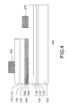
- FIG. 1 is a cross-sectional schematic view of an LED chip according to a first embodiment of the present invention.
- FIG. 2 is a cross-sectional schematic view of an LED chip according to a second embodiment of the present invention.
- FIG. 3 is a cross-sectional schematic view of an LED chip according to a third embodiment of the present invention.
- FIG. 4 is a cross-sectional schematic view of an LED chip according to a fourth embodiment of the present invention.
- FIG. 1 is a cross-sectional schematic view of an LED chip according to a first embodiment of the present invention.
- an LED chip 100 of the present invention comprises a chip 110 , a first type doped semiconductor layer 120 , a second type doped semiconductor layer 130 , a light emitting layer 140 , an Indium-doped Al x Ga 1-x N based material layer (0 ⁇ x ⁇ 1) 150 , a tunneling junction layer 160 , a first electrode 170 , and a second electrode 180 .
- the first type doped semiconductor layer 120 is disposed on the substrate 110
- the second type doped semiconductor layer 130 is disposed above the first type doped semiconductor layer 110 .
- the light emitting layer 140 is disposed between the first type doped semiconductor layer 120 and the second type doped semiconductor layer 130 .
- the first electrode 170 is disposed on the first type doped semiconductor layer 110
- the second electrode 180 is disposed on the second type doped semiconductor layer 130 .
- the Indium-doped Al x Ga 1-x N based material layer 150 is disposed on the upper surface of the light emitting layer 140 .
- the Indium-doped Al x Ga 1-x N based material layer 150 is disposed in the present invention to relieve the lattice mismatch between the material of the second type doped semiconductor layer 130 and that of the light emitting layer 140 , so as to reduce the stress generated by the LED chip 100 during the process of epitaxy. Also, since the dopant In has a superior surface migration capability, the LED chip 100 accordingly has a more planar surface.
- the dopant In can reduce the vacancy density of the element N, so as to promote the proportion of V/III during the process of epitaxy, thus improving the dislocation defects within the LED chip 100 .
- the tunneling junction layer 160 is disposed between the Indium-doped Al x Ga 1-x N based material layer 150 and the second type doped semiconductor layer 130 , so as to reduce the voltage drop between the second type doped semiconductor layer 130 and the light emitting layer 140 , thus the LED chip 100 of the present invention has a lower operation voltage. Furthermore, when the band-gap of the tunneling junction layer 160 is greater than that of the light emitting layer 140 , the LED chip 100 has a preferred light emitting property.
- the tunneling junction layer 160 comprises a first type Al x Ga 1-x N based material layer (0 ⁇ x ⁇ 1) 162 and a second type Al x Ga 1-x N based material layer (0 ⁇ x ⁇ 1) 164 .
- the second type Al x Ga 1-x N based material layer 164 is disposed between the Indium-doped Al x Ga 1-x N based material layer 150 and the first type Al x Ga 1-x N based material layer 162 .
- the first type Al x Ga 1-x N based material layer 162 can be n-type Al x Ga 1-x N based material layer
- the second type Al x Ga 1-x N based material layer 164 can be p-type Al x Ga 1-x N based material layer (thus, the first type doped semiconductor layer 120 and the second type doped semiconductor layer 130 can be n-type Al x Ga 1-x N based material layer and p-type Al x Ga 1-x N based material layer, respectively).
- the first type Al x Ga 1-x N based material layer 162 can be Silicon-doped, Indium-doped, or the combination thereof
- the second type Al x Ga 1-x N based material layer 164 can be Magnesium-doped, Indium-doped, or the combination thereof in the present invention. More particularly, when the first type Al x Ga 1-x N based material layer 162 is both Silicon-doped and Indium-doped, and the second type Al x Ga 1-x N based material layer 164 is both Magnesium-doped and Indium-doped, the LED chip 100 can obtain an even lower operation voltage.
- the above Indium-doped Al x Ga 1-x N based material layer 150 , the first type Al x Ga 1-x N based material layer 162 , and the second type Al x Ga 1-x N based material layer 164 are formed through, for example, Metal Organic Chemical Vapor Deposition (MOCVD), with a thickness preferably between 0.5 nm and 20 nm, and a preferred growth temperature between 800° C. and 1200° C.
- MOCVD Metal Organic Chemical Vapor Deposition
- each thin film layer and the substrate of the above LED chip 100 are described below respectively.
- the material of the substrate 110 comprises Sapphire mono crystal, silicon carbide (6H—SiC or 4H—SiC), Si, ZnO, GaAs, MgAl 2 O 4 , or other single crystal oxides with other lattice constant approximately to the nitride semiconductor, and the configuration of the material of the substrate 110 is, for example, C-Plane, E-Plane, or A-plane.
- the first type doped semiconductor layer 120 comprises a buffer layer 122 , a nucleation layer 124 , and a first type contact layer 126 .
- the buffer layer 122 disposed on the substrate 110 is made of, for example, Al a Ga b In 1-a-b N, (0 ⁇ a, b ⁇ 1, a+b ⁇ 1).
- the nucleation layer 124 is disposed on the buffer layer 122 , mainly for providing a faster subsequent epitaxy and enabling a more uniform lattice arrangement of the expitaxy.
- the first type contact layer 126 is disposed on the nucleation layer 124 .
- the second type doped semiconductor layer 130 comprises a second type contact layer 132 .
- the first type contact layer 126 is an n-type contact layer
- the second type contact layer 132 is a p-type contact layer
- the above contact layers are made of, for example, Al x Ga 1-x N based material (0 ⁇ x ⁇ 1), and the properties of the contact layers can be adjusted with different doped impurity ions and concentrations.
- the light emitting layer 140 is constructed as a structure of multiple quantum wells made of In a Ga 1-a N (0 ⁇ a ⁇ 1), and emits light of different wavelengths depending on the different proportions of the elements In and Ga.
- the first type doped semiconductor layer 120 further comprises a first type cladding layer (not shown) disposed on the first type contact layer 126 .
- the second type doped semiconductor layer 130 further comprises a second type cladding layer (not shown) disposed between the second contact layer 132 and the light emitting layer 140 .
- the tunneling junction layer 160 of this embodiment also has the property of a cladding layer, and thus the LED chip 100 can have preferred electrical properties without the second type cladding layer.
- an undoped Al x Ga 1-x N based material layer (0 ⁇ x ⁇ 1) can be used to replace the Indium-doped Al x Ga 1-x N based material layer 150 according to the present invention.
- the leakage current of the LED 100 can be significantly reduced in the present invention, so as to provide the LED 100 with preferred electrical properties.
- the undoped Al x Ga 1-x N based material layer is formed through for example, Metal-Organic Chemical Vapor Deposition (MOCVD), with a thickness preferably between 0.5 nm and 20 nm, and a preferred growth temperature between 800° C. and 1200° C.
- MOCVD Metal-Organic Chemical Vapor Deposition
- the Indium-doped Al x Ga 1-x N based material layer 150 and the tunneling junction layer 160 are by no means limited to be located between the second type doped semiconductor layer 130 and the light emitting layer 140 according to the present invention.
- the LEDs with other structures in the present invention are illustrated below through other embodiments with reference to the drawings.
- FIG. 2 is a cross-sectional view of the LED chip according to a second embodiment of the present invention.
- the LED chip 200 of the second embodiment is similar to the LED chip 100 (shown in FIG. 1 ) of the first embodiment; the difference is that the disposition of the Indium-doped Al x Ga 1-x N based material layer (0 ⁇ x ⁇ 1) 250 and the tunneling junction layer 260 are different.
- the Indium-doped Al x Ga 1-x N based material layer 250 is disposed on the lower surface of the light emitting layer 140
- the tunneling junction layer 260 is disposed between the Indium-doped Al x Ga 1-x N based material layer 250 and the fist type doped semiconductor layer 120 .
- the tunneling junction layer 260 comprises a first type Al x Ga 1-x N based material layer (0 ⁇ x ⁇ 1) 262 and a second type Al x Ga 1-x N based material layer (0 ⁇ x ⁇ 1) 264 , wherein the first type Al x Ga 1-x N based material layer 262 is disposed between the Indium-doped Al x Ga 1-x N based material layer 250 and the second type Al x Ga 1-x N based material layer 264 .
- the Indium-doped Al x Ga 1-x N based material layer 250 can reduce the lattice mismatch between the first type doped semiconductor layer 120 and the light emitting layer 140 , so as to provide the LED chip 200 with a more planar surface. Additionally, the tunneling junction layer 260 can reduce the voltage drop between the first type doped semiconductor layer 120 and the light emitting layer 140 , so as to provide the LED chip 200 with a lower operation voltage. Certainly, the undoped Al x Ga 1-x N based material layer can also be used to replace the Indium-doped Al x Ga 1-x N based material layer 250 so as to provide the LED chip 200 with a lower leakage current. It is to be mentioned that the tunneling junction layer 260 in this embodiment can also be used as a cladding layer to replace the above first type cladding layer that the electrical properties of the LED chip 200 can be improved.
- the number of the Indium-doped Al x Ga 1-x N based material layers and of the tunneling junction layers are not limited in the present invention.
- the LED chips 100 , 200 of the first embodiment and the second embodiment can be combined in the present invention, such that the Indium-doped Al x Ga 1-x N based material layer and the tunneling junction layer can be disposed between the light emitting layer and the first doped semiconductor layer, and disposed between the light emitting layer and the second doped semiconductor layer. Since this can be easily derived by those skilled in the art, it will not be depicted herein.
- the first type Al x Ga 1-x N based material layer is not limited to n-type Al x Ga 1-x N based material layer
- the second type Al x Ga 1-x N based material layer is not limited to p-type Al x Ga 1-x N based material layer according to the present invention.
- FIG. 3 is a cross-sectional view of the LED chip according to the third embodiment of the present invention
- FIG. 4 is a cross-sectional view of the LED chip according to a fourth embodiment of the present invention.
- the LED chip 300 of the third embodiment is similar to the LED chip 100 (shown in FIG. 1 ) of the first embodiment; the difference is that the first type Al x Ga 1-x N based material layer 362 of the tunneling junction layer 360 is a p-type Al x Ga 1-x N based material layer, and the second type Al x Ga 1-x N based material layer 364 is an n-type Al x Ga 1-x N based material layer.
- the first type Al x Ga 1-x N based material layer 362 of the tunneling junction layer 360 is a p-type Al x Ga 1-x N based material layer
- the second type Al x Ga 1-x N based material layer 364 is an n-type Al x Ga 1-x N based material layer.
- the LED chip 400 of the fourth embodiment is similar to the LED chip 200 of the second embodiment (shown in FIG. 2 ); the difference is that the first type Al x Ga 1-x N based material layer 462 of the tunneling junction layer 460 is a p-type Al x Ga 1-x N based material layer, and the second type Al x Ga 1-x N based material layer 464 is an n-type Al x Ga 1-x N based material layer.
- the first type Al x Ga 1-x N based material layer can be Magnesium-doped, Indium-doped, or the combination thereof
- the second type Al x Ga 1-x N based material layers 364 , 464 can be Silicon-doped, Indium-doped, or the combination thereof.
- the LED chips 300 , 400 can even have a lower operation voltage, respectively.
- the first type doped semiconductor layer 120 and the second type semiconductor layer 130 are required to be p-type Al x Ga 1-x N based material layer and n-type Al x Ga 1-x N based material layer, respectively.
- the undoped Al x Ga 1-x N based material layer can be used to replace the Indium-doped Al x Ga 1-x N based material layers 150 , 250 (shown in FIGS. 3 and 4 ) according to the present invention, so as to provide the LED chip 200 with lower leakage current.
- the LED chips 300 , 400 of the third embodiment and the fourth embodiment can be combined in the present invention, such that the Indium-doped Al x Ga 1-x N based material layer and the tunneling junction layer can be disposed between the light emitting layer and the first doped semiconductor layer, and disposed between the light emitting layer and the second doped semiconductor layer. Since this can be easily derived by those skilled in the art, it will not be depicted herein.
- the Indium-doped Al x Ga 1-x N based material layer (or the undoped Al x Ga 1-x N based material layer) and the tunneling junction layer are disposed between the light emitting layer and the first doped semiconductor layer, or disposed between the light emitting layer and the second doped semiconductor layer.
- the Indium-doped Al x Ga 1-x N based material layer (or the undoped Al x Ga 1-x N based material layer and the tunneling junction layer are not limited to be located at the above-described positions in the present invention.
- the Indium-doped Al x Ga 1-x N based material layer (or the undoped Al x Ga 1-x N based material layer) and the tunneling junction layer can be disposed between the second electrode and the second type contact layer, or disposed between the second type contact layer and the second type cladding layer, or disposed between the first type cladding layer and the first type contact layer, etc., to provide the LED chip with preferred quality.
- the LED chip of the present invention has the following advantages:
- the LED chip Since the Indium-doped Al x Ga 1-x N based material layer is disposed, the LED chip has a more planar surface, and the dislocation defects of the LED chip generated during the process of the epitaxy are eliminated.
- the undoped Al x Ga 1-x N based material layer is disposed, the leakage current of the LED chip can be reduced, so as to promote the electrical properties.
- the LED chip Since the tunneling junction layer can be used to effectively reduce the voltage drop between the first/second type doped semiconductor layers and the light emitting layer, the LED chip has a lower operation voltage.
- the operation voltage of the LED chip can be further reduced.
- the LED chip Since the tunneling junction layer has the property of a cladding layer, the LED chip obtains preferred electrical properties without the cladding layer.
Abstract
Description
Claims (20)
Applications Claiming Priority (3)
| Application Number | Priority Date | Filing Date | Title |
|---|---|---|---|
| TW94136676 | 2005-10-20 | ||
| TW094136676A TWI266440B (en) | 2005-10-20 | 2005-10-20 | Light emitting diode chip |
| TW94136676A | 2005-10-20 |
Publications (2)
| Publication Number | Publication Date |
|---|---|
| US20070090390A1 US20070090390A1 (en) | 2007-04-26 |
| US7763902B2 true US7763902B2 (en) | 2010-07-27 |
Family
ID=37984511
Family Applications (1)
| Application Number | Title | Priority Date | Filing Date |
|---|---|---|---|
| US11/536,694 Active US7763902B2 (en) | 2005-10-20 | 2006-09-29 | Light emitting diode chip |
Country Status (2)
| Country | Link |
|---|---|
| US (1) | US7763902B2 (en) |
| TW (1) | TWI266440B (en) |
Families Citing this family (2)
| Publication number | Priority date | Publication date | Assignee | Title |
|---|---|---|---|---|
| DE102008028036A1 (en) * | 2008-02-29 | 2009-09-03 | Osram Opto Semiconductors Gmbh | Optoelectronic semiconductor body with tunnel junction and method for producing such |
| US20140353578A1 (en) * | 2013-06-04 | 2014-12-04 | Epistar Corporation | Light-emitting device |
Citations (7)
| Publication number | Priority date | Publication date | Assignee | Title |
|---|---|---|---|---|
| US5577350A (en) | 1992-06-10 | 1996-11-26 | Musicdome Ventures, Inc. | Auditorium |
| WO2002093658A1 (en) | 2001-05-17 | 2002-11-21 | Emcore Corporation | Nitride semiconductor led with tunnel junction |
| US6515308B1 (en) * | 2001-12-21 | 2003-02-04 | Xerox Corporation | Nitride-based VCSEL or light emitting diode with p-n tunnel junction current injection |
| US6526082B1 (en) | 2000-06-02 | 2003-02-25 | Lumileds Lighting U.S., Llc | P-contact for GaN-based semiconductors utilizing a reverse-biased tunnel junction |
| US20030205718A1 (en) | 1995-07-24 | 2003-11-06 | Toyoda Gosei Co., Ltd | Light-emitting semiconductor device using group III nitride compound |
| US20040012014A1 (en) * | 2002-07-08 | 2004-01-22 | Sadanori Yamanaka | Epitaxial substrate for compound semiconductor light-emitting device, method for producing the same and light-emitting device |
| US6800876B2 (en) * | 2001-01-16 | 2004-10-05 | Cree, Inc. | Group III nitride LED with undoped cladding layer (5000.137) |
-
2005
- 2005-10-20 TW TW094136676A patent/TWI266440B/en active
-
2006
- 2006-09-29 US US11/536,694 patent/US7763902B2/en active Active
Patent Citations (7)
| Publication number | Priority date | Publication date | Assignee | Title |
|---|---|---|---|---|
| US5577350A (en) | 1992-06-10 | 1996-11-26 | Musicdome Ventures, Inc. | Auditorium |
| US20030205718A1 (en) | 1995-07-24 | 2003-11-06 | Toyoda Gosei Co., Ltd | Light-emitting semiconductor device using group III nitride compound |
| US6526082B1 (en) | 2000-06-02 | 2003-02-25 | Lumileds Lighting U.S., Llc | P-contact for GaN-based semiconductors utilizing a reverse-biased tunnel junction |
| US6800876B2 (en) * | 2001-01-16 | 2004-10-05 | Cree, Inc. | Group III nitride LED with undoped cladding layer (5000.137) |
| WO2002093658A1 (en) | 2001-05-17 | 2002-11-21 | Emcore Corporation | Nitride semiconductor led with tunnel junction |
| US6515308B1 (en) * | 2001-12-21 | 2003-02-04 | Xerox Corporation | Nitride-based VCSEL or light emitting diode with p-n tunnel junction current injection |
| US20040012014A1 (en) * | 2002-07-08 | 2004-01-22 | Sadanori Yamanaka | Epitaxial substrate for compound semiconductor light-emitting device, method for producing the same and light-emitting device |
Non-Patent Citations (4)
| Title |
|---|
| C. K. Shu et al. "Isoelectronic In-doping effect in GaN films grown by metalorganic chemical vapor deposition." Applied Physics Letters. Aug. 3, 1998. vol. 73. No. 5. pp. 641-643. American Institute of Physics. |
| Cheng-Huang Kuo et al. "GaN-Based Light Emitting Diodes with Si-Doped In0.23Gn0.77N/GaN Short Period Superlattice Current Spreading Layer." Jpn. J. Appl. Phys. vol. 42(2003). pp. 2270-2272. Part 1. No. 4B. Apr. 2003. The Japan Society of Applied Physics. |
| F. C. Chang et al. "Characteristics of p-type GaN Films Doped with Isoelectronic Indium Atoms." Chinese Journal of Physics, Dec. 2002, vol. 40, No. 6. pp. 637-643. The Physical Society of the Republic of China. |
| H. M. Chung et al "Electrical characterization of Isoelectronic In-doping effects in GaN films grown by metalorganic vapor phase epitaxy." Applied Physics Letters. Feb. 14, 2000. vol. 76 No. 7. pp. 897-899. American Institute of physics. |
Also Published As
| Publication number | Publication date |
|---|---|
| TW200717844A (en) | 2007-05-01 |
| TWI266440B (en) | 2006-11-11 |
| US20070090390A1 (en) | 2007-04-26 |
Similar Documents
| Publication | Publication Date | Title |
|---|---|---|
| TW475275B (en) | Vertical geometry ingan led | |
| US9911898B2 (en) | Ultraviolet light-emitting device | |
| US7868316B2 (en) | Nitride semiconductor device | |
| US7429756B2 (en) | Nitride semiconductor light emitting device | |
| US6943381B2 (en) | III-nitride light-emitting devices with improved high-current efficiency | |
| RU2523747C2 (en) | Boron-containing iii-nitride light-emitting device | |
| US20080191191A1 (en) | Light Emitting Diode of a Nanorod Array Structure Having a Nitride-Based Multi Quantum Well | |
| US20150255673A1 (en) | Nitride semiconductor light-emitting device and method for producing the same | |
| US7964882B2 (en) | Nitride semiconductor-based light emitting devices | |
| US8519414B2 (en) | III-nitride based semiconductor structure with multiple conductive tunneling layer | |
| US20120145991A1 (en) | High-quality non-polar/semi-polar semiconductor element on tilt substrate and fabrication method thereof | |
| KR20040016723A (en) | Nitride semiconductor LED and fabrication method for thereof | |
| KR100649496B1 (en) | Nitride semiconductor light emitting device and method of manufacturing the same | |
| KR102115752B1 (en) | Optoelectronic devices incorporating single crystalline aluminum nitride substrate | |
| US10651340B2 (en) | Reducing or eliminating nanopipe defects in III-nitride structures | |
| TW201717429A (en) | Semiconductor light-emitting device | |
| US20080078439A1 (en) | Polarization-induced tunnel junction | |
| US8865494B2 (en) | Manufacturing method for compound semiconductor light-emitting element | |
| US20200343412A1 (en) | Light-emitting element and method for manufacturing light-emitting element | |
| CN114824019A (en) | Semiconductor light-emitting element | |
| TW200414569A (en) | Group-III nitride semiconductor device, production method thereof and light-emitting diode | |
| KR100838195B1 (en) | Method for fabricating a light emitting diode of a nitride compound semiconductor and a light emitting diode fabricated by the method | |
| US7763902B2 (en) | Light emitting diode chip | |
| US7812354B2 (en) | Alternative doping for group III nitride LEDs | |
| CN101859839A (en) | Light-emitting diode (LED) chip |
Legal Events
| Date | Code | Title | Description |
|---|---|---|---|
| AS | Assignment |
Owner name: FORMOSA EPITAXY INCORPORATION, TAIWAN Free format text: ASSIGNMENT OF ASSIGNORS INTEREST;ASSIGNORS:WU, LIANG-WEN;CHIEN, FEN-REN;REEL/FRAME:018396/0627 Effective date: 20060925 |
|
| STCF | Information on status: patent grant |
Free format text: PATENTED CASE |
|
| FEPP | Fee payment procedure |
Free format text: PAT HOLDER NO LONGER CLAIMS SMALL ENTITY STATUS, ENTITY STATUS SET TO UNDISCOUNTED (ORIGINAL EVENT CODE: STOL); ENTITY STATUS OF PATENT OWNER: LARGE ENTITY |
|
| SULP | Surcharge for late payment | ||
| FPAY | Fee payment |
Year of fee payment: 4 |
|
| AS | Assignment |
Owner name: EPISTAR CORPORATION, TAIWAN Free format text: ASSIGNMENT OF ASSIGNORS INTEREST;ASSIGNOR:FORMOSA EPITAXY INCORPORATION;REEL/FRAME:040149/0765 Effective date: 20160922 |
|
| MAFP | Maintenance fee payment |
Free format text: PAYMENT OF MAINTENANCE FEE, 8TH YEAR, LARGE ENTITY (ORIGINAL EVENT CODE: M1552) Year of fee payment: 8 |
|
| MAFP | Maintenance fee payment |
Free format text: PAYMENT OF MAINTENANCE FEE, 12TH YEAR, LARGE ENTITY (ORIGINAL EVENT CODE: M1553); ENTITY STATUS OF PATENT OWNER: LARGE ENTITY Year of fee payment: 12 |