US7761833B2 - Semiconductor device and dummy pattern arrangement method - Google Patents
Semiconductor device and dummy pattern arrangement method Download PDFInfo
- Publication number
- US7761833B2 US7761833B2 US12/103,028 US10302808A US7761833B2 US 7761833 B2 US7761833 B2 US 7761833B2 US 10302808 A US10302808 A US 10302808A US 7761833 B2 US7761833 B2 US 7761833B2
- Authority
- US
- United States
- Prior art keywords
- dummy
- wiring
- pattern
- patterns
- region
- Prior art date
- Legal status (The legal status is an assumption and is not a legal conclusion. Google has not performed a legal analysis and makes no representation as to the accuracy of the status listed.)
- Expired - Fee Related, expires
Links
Images


Classifications
-
- H—ELECTRICITY
- H01—ELECTRIC ELEMENTS
- H01L—SEMICONDUCTOR DEVICES NOT COVERED BY CLASS H10
- H01L23/00—Details of semiconductor or other solid state devices
- H01L23/52—Arrangements for conducting electric current within the device in operation from one component to another, i.e. interconnections, e.g. wires, lead frames
- H01L23/522—Arrangements for conducting electric current within the device in operation from one component to another, i.e. interconnections, e.g. wires, lead frames including external interconnections consisting of a multilayer structure of conductive and insulating layers inseparably formed on the semiconductor body
-
- H—ELECTRICITY
- H01—ELECTRIC ELEMENTS
- H01L—SEMICONDUCTOR DEVICES NOT COVERED BY CLASS H10
- H01L2924/00—Indexing scheme for arrangements or methods for connecting or disconnecting semiconductor or solid-state bodies as covered by H01L24/00
- H01L2924/0001—Technical content checked by a classifier
- H01L2924/0002—Not covered by any one of groups H01L24/00, H01L24/00 and H01L2224/00
Definitions
- the present invention relates to a semiconductor device and dummy pattern arrangement method.
- a semiconductor device has recently been developed to be more multi-layered.
- the wiring layer in an upper layer is influenced by convex/concave in the surface of the wiring layer in a lower layer. If this influence is large, there is a possibility that disconnection is occurred in wirings in the wiring layer formed in the upper layer in some cases. Even in the same wiring layer, the wirings may be disconnected due to partial convex/concave.
- a technique for arranging dummy patterns for each of the plurality of wiring layers in a region where the wiring patterns are not formed see Japanese Unexamined Patent Application Publication No. 2002-368088, Japanese Unexamined Patent Application Publication No. 2000-277615, Japanese Unexamined Patent Application Publication No. 2003-140319, and Japanese Unexamined Patent Application Publication No. 2004-253655).
- Japanese Unexamined Patent Application Publication No. 2002-368088 discloses a technique for simplifying capacity calculation of parasitic capacity added to the wiring patterns by making distance between the dummy patterns and the wiring patterns constant.
- Japanese Unexamined Patent Application Publication No. 2000-277615 discloses a technique arranging the dummy patterns having different densities in a region where the wiring patterns of the wiring region are not arranged.
- the distance between the dummy pattern and the wiring pattern has been decreased.
- a resist may lie during a manufacturing process and the wiring pattern and the dummy pattern may be connected (shorted out) by dust (defect).
- Japanese Unexamined Patent Application Publication No. 2002-368088 discloses a layout where dummy patterns are arranged continuously in the direction perpendicular to the wiring patterns extending in one direction. Although the dummy patterns are arranged separately from the wiring patterns, if one end of the dummy pattern and the wiring pattern are shorted out by dust, the capacity of the dummy pattern is added to the wiring pattern.
- Japanese Unexamined Patent Application Publication No. 2000-277615 there is disclosed a technique arranging dummy patterns having different densities.
- the dummy patterns having low metal densities are arranged close to the wiring patterns and therefore it is suppressed that the wiring capacity is added to the wiring pattern by dust.
- data amount required to execute dummy pattern arrangement process is increased.
- Japanese Unexamined Patent Application Publication No. 2000-277615 arrangement region of the pattern is divided into a plurality of blocks, and pattern having high metal density and pattern having low metal density are arranged in each block.
- the arrangement position of each pattern is identified using apex information (apex coordinate or the like) of each pattern included in the wiring data (layout data) Therefore, the technique for dividing the wiring region into the plurality of blocks as in Japanese Unexamined Patent Application Publication No. 2000-277615 requires setting the apex information of the pattern for each block after being divided, which increases data amount required for dummy pattern arrangement.
- the number of blocks that is set reaches 2.5*10 9 .
- the apex information of the dummy patterns corresponding to the number of blocks that are set is needed and data amount required for dummy pattern arrangement is increased.
- the increase in the data amount required for dummy pattern arrangement causes longer time for wiring process and memory shortage of the wiring device.
- an arrangement method for preventing the decrease of the reliability of the semiconductor device due to the attachment of dust between the patterns without increasing data amount for dummy pattern arrangement is required.
- a semiconductor device having a dummy pattern arrangement layout for preventing the decrease of the reliability of the semiconductor device due to the dust attachment between the patterns is also required.
- a semiconductor device includes a plurality of wiring patterns arranged in a first wiring layer of the semiconductor device and extending in a first direction, and a plurality of dummy patterns arranged in the first wiring layer and extending in a second direction different from the first direction, wherein each of the plurality of dummy patterns is arranged spaced apart from each of the plurality of wiring patterns and includes one or more dummy lands formed by separating a part of the dummy pattern opposed to the wiring pattern, from the rest part of the dummy pattern.
- a dummy pattern arrangement method using a computer includes reading arrangement data where first and second wiring patterns are arranged in a first region, the first and second wiring patterns extending along a first axis line, arranging one or more dummy patterns in the first region in such a manner that the dummy pattern extends along a second axis line different from the first axis line and is separated from the first and second wiring patterns, and processing a first end of the dummy pattern to form a first dummy land at the first wiring pattern side.
- FIG. 1 is a schematic diagram showing a configuration of a dummy pattern arrangement device according to a first embodiment
- FIG. 2 is a configuration diagram of a wiring region 10 A according to the first embodiment
- FIG. 3 is a flow chart showing a dummy pattern arrangement process according to the first embodiment
- FIGS. 4A and 4B are explanation diagrams explaining processing of the dummy patterns
- FIG. 5 is a configuration diagram of a wiring region 10 B according to a second embodiment
- FIG. 6 is a flow chart showing a dummy pattern arrangement process according to the second embodiment
- FIG. 7 is a schematic perspective diagram of a semiconductor device according to a third embodiment.
- FIG. 8 is a configuration diagram where patterns of a wiring region 10 C are superimposed on the wiring region 10 A of the first embodiment
- FIG. 9 is a configuration diagram showing patterns of the wiring region 10 C.
- FIG. 10 is an explanation diagram of a parasitic capacity C 1 formed in laminating direction
- FIG. 11 is a flow chart showing a dummy pattern arrangement process according to a third embodiment
- FIG. 12 is a partial configuration diagram of a wiring region
- FIG. 13 is a schematic perspective diagram of a semiconductor device according to a fourth embodiment.
- FIG. 14 is a configuration diagram of the wiring region 10 A of the first embodiment superimposed on the patterns of a wiring region 10 D;
- FIG. 15 is a configuration diagram showing patterns of the wiring region 10 D.
- FIG. 16 is an explanation diagram of a parasitic capacity C 2 formed in laminating direction.
- FIG. 17 is a flow chart showing a dummy pattern arrangement process according to a third embodiment.
- FIG. 1 shows a block diagram showing a schematic configuration of a dummy pattern arrangement device.
- FIG. 2 shows a wiring region (first region) 10 A after dummy pattern arrangement process.
- FIG. 3 shows a flow of the dummy pattern arrangement process.
- FIGS. 4A and 4B show explanation diagrams showing states before and after pattern processing. Note that the process for dummy pattern arrangement is executed by a computer.
- FIG. 1 shows a block diagram showing a schematic configuration of a dummy pattern arrangement device 50 .
- the dummy pattern arrangement device 50 includes a storage 51 and a processing unit 52 .
- the storage 51 stores information of arrangement data, wiring rule or the like.
- the processing unit 52 reads out the information stored in the storage 51 and executes the dummy pattern arrangement process described in FIG. 3 .
- the processing unit 52 includes a data rate verification unit 53 , a pattern arrangement unit 54 , a pattern detection unit 55 , and a pattern processing unit 56 .
- the data rate verification unit 53 calculates the data rate of patterns arranged in a wiring region.
- the pattern arrangement unit 54 arranges the patterns in the wiring region.
- the pattern detection unit 55 searches and detects the patterns arranged in the wiring region.
- the pattern processing unit 56 processes the patterns detected by the pattern detection unit 55 .
- functions of the data rate verification unit 53 , the pattern arrangement unit 54 , the pattern detection unit 55 , and the pattern processing unit 56 are realized by sequentially executing orders of programs in a processing unit.
- the program itself may be stored either in the storage 51 or other storage devices (memory or the like).
- FIG. 2 shows a wiring region (first region) 10 A after the dummy pattern arrangement process.
- the wiring region 10 A is a two-dimensional planar region.
- a plurality of wiring patterns 11 a to 11 j and a plurality of dummy patterns 12 a to 12 f are arranged in the wiring region 10 A.
- the plurality of dummy patterns 12 a to 12 f are arranged in the wiring region 10 A after the plurality of wiring patterns 11 a to 11 j are arranged.
- the dummy patterns 12 a to 12 f are arranged according to a wiring rule (wiring width, wiring interval or the like) same to that of the wiring patterns 11 a to 11 j.
- the wiring patterns 11 a to 11 j extend along x axis (first axis line) and are rectangular patterns. Longitudinal direction of the wiring patterns 11 a to 11 j is x axis.
- the dummy patterns 12 a to 12 f extend along y axis (second axis line).
- the dummy patterns 12 a to 12 f are formed by three dummy lands.
- the dummy lands forming each of the dummy patterns 12 a to 12 f are formed by separating both ends (both end parts) of the rectangular dummy patterns having longitudinal direction of y axis. Note that the dummy land means the pattern that is left after the dummy pattern is partially removed.
- the x axis and the y axis are perpendicular to each other. Therefore, the extending direction of the wiring patterns 11 a to 11 j and the extending direction of the dummy patterns 12 a to 12 f are perpendicular to each other.
- the pattern detection unit 55 of the processing unit 52 can identify each of the dummy patterns and the wiring patterns based on a difference in extending direction of the pattern.
- each of the dummy patterns 12 a to 12 f are arranged between the wiring patterns that are adjacent with each other.
- the dummy patterns 12 a to 12 f are arranged separately from the adjacent wiring patterns.
- the dummy pattern 12 a is arranged between the wiring pattern 11 a and the wiring pattern 11 f and separately from the wiring pattern 11 a and the wiring pattern 11 f .
- the dummy pattern 12 b is arranged in a same way as the dummy pattern 12 a.
- the dummy pattern 12 c is arranged between the wiring pattern 11 b and the wiring pattern 11 e and separately from the wiring pattern 11 b and the wiring pattern 11 e .
- the dummy pattern 12 d is arranged in a same way as the dummy pattern 12 c.
- the dummy pattern 12 e is arranged between the wiring pattern 11 c and the wiring pattern 11 h and separately from the wiring pattern 11 c and the wiring pattern 11 h .
- the dummy pattern 12 f is arranged in a same way as the dummy pattern 12 e .
- the dummy patterns 12 a to 12 f are arranged in the wiring region 10 A by the pattern arrangement unit 54 of the processing unit 52 .
- the dummy patterns 12 a to 12 f extend along y axis perpendicular to x axis (extending direction of the wiring patterns 11 a to 11 j ).
- the dummy patterns are arranged extending along the direction perpendicular to the extending direction of the wiring patterns as in the present embodiment, attachment of dust can be a problem only on one ends of the dummy patterns.
- the dummy patterns extend in the same direction to that of the wiring patterns, attachment of dust can be a problem in a region from one ends to the other ends of the dummy patterns.
- the dummy patterns 12 a to 12 f are arranged along y axis perpendicular to x axis (first axis line) where the wiring patterns 11 a to 11 j extend. Therefore, it is possible to lower chances to add the wiring capacity of the dummy pattern to the wiring pattern by dust attached therebetween.
- the dummy patterns 12 a to 12 f are formed by three dummy lands.
- Each of the dummy patterns 12 a to 12 f is formed by separating both ends of the rectangular patterns having longitudinal direction of y axis. Since both ends of the rectangular patterns are separated, the dummy patterns 12 a to 12 f are formed of dummy lands 14 a to 14 f forming main parts of the patterns, dummy lands 13 a to 13 f forming one ends of the patterns (one end parts (first ends)), and dummy lands 15 a to 15 f forming the other ends of the patterns (the other end parts (second ends)).
- the width along y axis of each of the dummy lands 13 a to 13 f forming one ends of the patterns is substantially equal to the width along y axis of each of the dummy lands 15 a to 15 f forming the other ends of the patterns.
- the width along the y axis of each of the dummy lands 14 a to 14 f forming the main parts of the patterns is wider than the width along the y axis of each of the dummy lands forming end parts of the pattern above.
- Each dummy pattern is formed by three dummy lands as follows.
- the dummy pattern 12 a is formed by the dummy land 13 a in the wiring pattern 11 a side, the dummy land 15 a in the wiring pattern 11 f side, and the dummy land 14 a between the dummy land 13 a and the dummy land 15 a .
- the dummy pattern 12 b is formed by the dummy land 13 b in the wiring pattern 11 a side, the dummy land 15 b in the wiring pattern 11 f side, and the dummy land 14 b between the dummy land 13 b and the dummy land 15 b .
- the dummy pattern 12 c is formed by the dummy land 13 c in the wiring pattern 11 b side, the dummy land 15 c in the wiring pattern 11 e side, and the dummy land 14 c between the dummy land 13 c and the dummy land 15 c .
- the dummy pattern 12 d is formed by the dummy land 13 d in the wiring pattern 11 b side, the dummy land 15 d in the wiring pattern 11 e side, and the dummy land 14 d between the dummy land 13 d and the dummy land 15 d .
- the dummy pattern 12 e is formed by the dummy land 13 e in the wiring pattern 11 c side, the dummy land 15 e in the wiring pattern 11 h side, and the dummy land 14 e between the dummy land 13 e and the dummy land 15 e .
- the dummy pattern 12 f is formed by the dummy land 13 f in the wiring pattern 11 c side, the dummy land 15 f in the wiring pattern 11 h side, and the dummy land 14 f between the dummy land 13 f and the dummy land 15 f.
- the value of the wiring capacity added to the wiring pattern 11 a can be made minimum since the dummy lands 13 a and 13 b are arranged in the wiring pattern 11 a side. Therefore, it is possible to make the wiring capacity of the dummy patterns added to the wiring pattern 11 a partial (the dummy land 13 a forming the dummy pattern 12 a and the dummy land 13 b forming the dummy pattern 12 b ). In other words, it is possible to prevent the wiring capacity of whole pattern before the dummy land 13 a or the dummy land 13 b is formed from being added to the wiring pattern 11 a .
- the value of the wiring capacity added to the wiring pattern 11 b can be made minimum since the dummy lands 13 c and 13 d are arranged in the wiring pattern 11 b side.
- This explanation can be applied to the other end sides of the dummy patterns 12 c and 12 d .
- the value of the wiring capacity added to the wiring pattern 11 c can be made minimum by the dummy lands 13 e and 13 f arranged in the wiring pattern 11 c side.
- the dummy lands forming the main parts of the patterns are formed wider in y axis direction than the dummy lands forming the ends of the patterns as will be clear from the drawing.
- the dummy patterns extending in the direction perpendicular to the extending direction of the wiring patterns are arranged in the wiring region. Therefore, it is possible to lower chances to connect the wiring pattern with the dummy pattern by dust. Further, the dummy lands forming the dummy patterns are arranged in the wiring pattern side. Therefore, even when dust is attached between the wiring pattern and the dummy pattern, the value of the wiring capacity added unintentionally to the wiring pattern can be made small. As a result, reliability of the behavior of the semiconductor device including such a wiring layer can be improved.
- the dummy patterns may be in floating state or may be fixed to power supply potential or ground potential.
- the processing unit 52 of the dummy pattern arrangement device 50 reads out data where the wiring patterns 11 a to 11 j are arranged in the wiring region 10 A (arrangement data) from the storage 51 as the data before the dummy pattern arrangement process.
- the data rate verification unit 53 of the dummy pattern arrangement device 50 checks whether the data rate of the arrangement data that is read in the wiring region 10 A exceeds a predetermined data ratio (S 1 ). Note that the data rate is equal to occupation rate of the patterns in the wiring region 10 A. In this step, it is checked whether the occupation rate of the wiring patterns 11 a to 11 j in the wiring region 10 A satisfies a predetermined occupation rate. When the checked data rate satisfies the predetermined data rate, the dummy pattern is not arranged in the wiring region 10 A any more.
- the pattern arrangement unit 54 of the dummy pattern arrangement device 50 arranges the dummy patterns in the wiring region 10 A (S 2 ). More specifically, the plurality of rectangular dummy patterns having longitudinal direction of y axis are arranged in the wiring region 10 A where the wiring patterns 11 a to 11 j are not arranged.
- the region where the wiring patterns 11 a to 11 j are arranged can be determined based on attribute information (positional information of start points (one ends), positional information of endpoints (the other ends), and pattern width) of the wiring patterns 11 a to 11 j .
- the area where the wiring patterns 11 a to 11 j are not arranged is determined by determining the area where the wiring patterns 11 a to 11 j are arranged. Then the plurality of dummy patterns are arranged in the region where the determined wiring patterns 11 a to 11 j are not arranged. Note that the attribute information of the wiring patterns is stored in the storage 51 of the dummy pattern arrangement device 50 . Note that the wiring rule of the dummy patterns that will be wired is the same to the wiring rule of the wiring patterns 11 a to 11 j . Arranging the dummy patterns corresponds to adding the attribute information of the dummy patterns to the arrangement data.
- the pattern detection unit 55 of the dummy pattern arrangement device 50 searches and detects the dummy patterns arranged in the wiring region 10 A (S 3 ). More specifically, the dummy patterns and the wiring patterns have different longitudinal directions as described above, therefore, based on this difference, the dummy patterns are distinguished from the wiring patterns. Note that the longitudinal direction of the patterns can be determined based on the attribute information of the patterns (positional information of the start points, positional information of end points, and pattern width).
- the pattern arrangement unit 54 can set new attributes specific to the dummy patterns and distinguish the wiring patterns from the dummy patterns based on these attributes.
- the pattern processing unit 56 of the dummy pattern arrangement device 50 processes both end parts of each of the plurality of detected dummy patterns (S 4 ).
- the pattern processing unit 56 processes the dummy patterns so that the both end parts thereof are separated.
- the separated ends are identified based on the attribute information of the dummy patterns (positional information of start points (one ends), positional information of end points (the other ends)).
- the processing of the dummy patterns is executed based on minimum area and minimum wiring interval of the patterns that are predetermined as the wiring rule.
- Each of the dummy patterns arranged on the wiring region 10 A becomes dummy patterns formed by the three dummy lands by the process of the pattern processing unit 56 (see FIG. 2 ). Note that the processing of the dummy patterns by the pattern processing unit 56 is realized by generating the attribute information of the dummy lands based on the attribute information of the dummy patterns.
- FIG. 4A shows an explanation diagram showing a state before the dummy pattern processing.
- FIG. 4B shows an explanation diagram showing a state after the dummy pattern processing.
- the dummy pattern 12 a is arranged in the wiring region 10 A.
- One end of the dummy pattern 12 a can be identified by coordinate a.
- the other end of the dummy pattern 12 a can be identified by coordinate b.
- FIG. 4B shows the dummy pattern 12 a of FIG. 4A .
- the pattern processing unit 56 processes the dummy pattern 12 a so that the dummy pattern 12 a is formed by the three dummy lands ( 13 a to 15 a ). More specifically, the pattern processing unit 56 identifies the end of the dummy pattern 12 a based on the coordinate a. Then the pattern processing unit 56 processes the end of the dummy pattern 12 a so that the area of the dummy land 13 a accords with minimum area (predetermined area) of the pattern set in the predetermined wiring rule.
- the size of the dummy land 13 a can be any, it is desirable to make the dummy land 13 a small in order to prevent the wiring capacity from being increased. Therefore, the area of the dummy land 13 a is set to be equal to the minimum area of the pattern set by the wiring rule.
- coordinate information of the end of the dummy land 13 a in the dummy land 14 a side and coordinate information of the end of the dummy land 14 a in the dummy land 13 a side are generated by the processing of coordinate a side of the dummy pattern 12 a .
- the coordinate of the end of the dummy land 13 a in the dummy land 14 a side is identified based on the coordinate a and the minimum area.
- the coordinate of the end of the dummy land 14 a in the dummy land 13 a side is identified based on the coordinate a, the minimum area, and space c.
- generating the dummy land 13 a in the dummy land 12 a corresponds to generating information indicating the coordinate of the end of the dummy land 13 a in the dummy land 14 a side and the coordinate of the end of the dummy land 14 a in the dummy land 13 a side.
- the data rate verification unit 53 of the dummy pattern arrangement device 50 checks whether the data rate in the wiring region 10 A after the dummy pattern arrangement satisfies the predetermined data rate (S 5 ). More specifically, it is checked whether the occupation rate of the wiring patterns and the dummy patterns in the wiring region 10 A satisfies the predetermined occupation rate. When the checked data rate satisfies the predetermined data rate, the dummy patterns are not arranged in the wiring region 10 A any more. When the checked data rate does not satisfy the predetermined data rate, the step goes back to S 2 as above.
- the dummy patterns extending in the direction perpendicular to the extending direction of the wiring patterns are arranged in the wiring region. Therefore, it is possible to lower chances to connect the wiring pattern with the dummy pattern by dust. Further, the dummy lands forming the dummy patterns are arranged in the wiring pattern side. Therefore, even when dust is attached between the wiring pattern and the dummy pattern, the value of the wiring capacity added unintentionally to the wiring pattern can be made small. As a result, reliability of the semiconductor device including such a wiring layer can be improved.
- This embodiment does not arrange the dummy patterns having different sizes for each region. Therefore, data amount required in the dummy pattern arrangement process does not press the capacity of the storage 51 of the dummy pattern arrangement device 50 .
- FIG. 5 shows a wiring region 10 B.
- FIG. 6 shows a flow of the dummy pattern arrangement process according to this embodiment.
- the dummy patterns according to the present embodiment are formed by five dummy lands and two dummy lands are included in each of the both end parts.
- each of the dummy patterns according to the present embodiment includes two dummy lands forming one end part of the pattern and two dummy lands forming the other end part of the pattern in addition to the dummy land forming the main part of the pattern.
- the width along the y axis of each of the dummy lands forming the main parts of the patterns is wider than the width along the y axis of each of the dummy land forming the ends of the patterns.
- the width along the y axis of each of the dummy lands forming the ends of the patterns is equal to each other and equal to the width of each of the dummy lands forming the ends of the patterns in the first embodiment.
- the dummy lands forming the main parts of the patterns are arranged in position spaced further apart from the wiring patterns compared with the first embodiment. Therefore, even when larger dust is attached between the wiring pattern and the dummy pattern, only the dummy land forming the end of the pattern closer to the wiring pattern is connected to the wiring pattern. The dummy land forming the main part of the pattern is not connected to the wiring pattern. Therefore, even when dust is attached between the wiring pattern and the dummy pattern, the value of the wiring capacity added unintentionally to the wiring pattern can be made smaller.
- the wiring capacity of the dummy pattern added to the wiring pattern can be made partial.
- the dummy pattern 12 f includes dummy lands 13 f and 16 f in the wiring pattern 11 c side and dummy lands 15 f and 17 f in the wiring pattern 11 h side.
- the dummy pattern 12 f includes a dummy land 14 f between the dummy lands 13 f and 16 f and the dummy lands 15 f and 17 f .
- the dummy pattern 12 f includes five dummy lands of the dummy land 13 f , the dummy land 16 f , the dummy land 14 f , the dummy land 17 f , and the dummy land 15 f from the wiring 11 c side to the wiring 11 h side.
- the dummy land 14 f has wider width along y axis than the width of each of the dummy lands 13 f , 16 f , 15 f , and 17 f.
- the dummy land 13 f and the dummy land 15 f are formed by separating both end parts of rectangular dummy pattern having longitudinal direction of y axis by the pattern processing unit 56 .
- the dummy land 16 f and the dummy land 17 f are formed by separating both end parts of the dummy land 14 f formed in forming the dummy land 13 f and the dummy land 15 f by the pattern processing unit 56 .
- the dummy land 16 f can also be formed by separating one end part of the dummy land 13 f that is formed in large shape. The same explanation can be applied to the dummy land 17 f.
- the dummy land 14 f forming the dummy pattern 12 f (dummy land forming the main part of the pattern) is formed in S 4 .
- the pattern processing unit 56 processes both end parts of the dummy land 14 f (S 6 ), the dummy land 16 f is arranged in the wiring pattern 11 c side, and the dummy land 17 f is arranged in the wiring pattern 11 h side. Note that the processing of the dummy land 17 f is executed similarly to the description regarding FIG. 4 as above.
- S 6 it is checked whether the data rate satisfies the predetermined data rate (S 5 ) as in the first embodiment.
- the present embodiment it is possible to make the value of the wiring capacity unintentionally added to the wiring pattern smaller even when larger dust is attached between the wiring pattern and the dummy pattern compared with the first embodiment.
- FIG. 7 shows a schematic perspective view of a semiconductor device SD 1 according to the present embodiment.
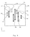
- FIG. 8 shows a configuration diagram where the patterns of the wiring region 10 C are superimposed on the wiring region 10 A (see first embodiment).
- FIG. 9 shows the patterns of the wiring region 10 C. Note that the wiring region 10 C is formed in the wiring layer of the upper layer of the wiring layer where the wiring region 10 A is formed.
- FIG. 10 shows an explanation diagram of the capacity formed in laminating direction.
- FIG. 11 shows a flow of the dummy pattern arrangement process according to the third embodiment.
- FIG. 12 shows an explanation diagram of the pattern after S 8 (see FIG. 11 ).
- the dummy patterns are arranged in the wiring region 10 A in consideration of the position of the wiring patterns arranged in the wiring region (second region) 10 C of the wiring layer of the upper layer. Therefore, the value of the capacity added to the wiring pattern can be made smaller.
- the description will be made more particularly.
- the semiconductor device SD 1 includes a wiring layer (first wiring layer) L 1 and a wiring layer (second wiring layer) L 2 .
- the semiconductor device SD 1 is formed by laminating the wiring layer L 1 and the wiring layer L 2 . Note that the wiring layer L 1 and the wiring layer L 2 are spaced apart with each other in FIG. 7 for the sake of convenience.
- the upper surface of the wiring layer L 1 corresponds to the wiring region 10 A according to the first embodiment.
- the upper surface of the wiring layer L 2 corresponds to the wiring region 10 C described below.
- the wiring layer L 1 and the wiring layer L 2 are laminated with each other so that the wiring region 10 A and the wiring region 10 C are superimposed with each other. Note that the wiring region 10 A and the wiring region 10 C are superimposed with each other with interlayer insulating film therebetween.
- the wiring region 10 C corresponding to the upper surface of the wiring layer L 2 is superimposed on the wiring region 10 A corresponding to the upper surface of the wiring layer L 1 .
- the wiring patterns 20 a to 20 e are formed in the wiring region 10 C.
- the wiring patterns 20 a to 20 e are the patterns extending along y axis and the rectangular patterns having longitudinal direction of y axis. Note that the extending direction of the wiring patterns 20 a to 20 e in the wiring region 10 C and the extending direction of the wiring patterns 11 a to 11 j in the wiring region 10 A are perpendicular to each other. Due to such a configuration, sum of the wiring length in the semiconductor device configured by multi-layered wiring layer can be made minimum.
- the wiring pattern 20 a of the wiring region 10 C connects the wiring pattern 11 c and the wiring pattern 11 f of the wiring region 10 A.
- the wiring pattern 20 b connects the wiring pattern 11 e and the wiring pattern 11 i .
- the wiring pattern 20 c connects the wiring pattern 11 b and the wiring pattern 11 h .
- the wiring pattern 20 d connects the wiring pattern 11 d and the wiring pattern 11 f and the wiring pattern 11 j .
- the wiring pattern 20 e connects the wiring pattern 11 g and other wiring pattern formed in the upper layer.
- the dummy patterns 12 a to 12 f arranged in the wiring region 10 A are arranged in the wiring region 10 A so as not to overlap with the wiring patterns 20 a to 20 e formed in the wiring region 10 C. Therefore, the size of the parasitic capacity C 1 in laminating direction formed between the dummy pattern 12 of the wiring region 10 A and the wiring pattern 20 of the wiring region 10 C can be minimized.
- the dummy patterns 12 a to 12 f of the wiring region 10 A are shown in dotted lines.
- the parasitic capacity formed in the laminating direction will be described with reference to FIG. 10 .
- the parasitic capacity is formed between the dummy pattern 12 a and the wiring pattern 20 (parasitic capacity C 1 is formed between the dummy land 13 a and the wiring pattern 20 ).
- the parasitic capacity C 1 formed between the dummy land 13 a and the wiring pattern 20 is added to the wiring pattern 11 in addition to the wiring capacity of the dummy pattern 13 a.
- the dummy pattern 12 a is arranged in the wiring region 10 A so as not to overlap with the wiring pattern 20 in consideration of the wiring pattern 20 of the wiring region 10 C of the upper layer as described above. Therefore, the value of the parasitic capacity formed between the dummy pattern 12 a and the wiring pattern 20 can be made small (smaller than the parasitic capacity C 1 formed when the dummy pattern 12 a is arranged so as to overlap with the wiring pattern 20 ). Even when the wiring pattern 11 and the dummy land 13 a in the wiring region 10 A are connected by dust, the parasitic capacity of the laminating direction that is added to the wiring pattern 11 (parasitic capacity between the dummy land 13 a and the wiring pattern 20 ) can be made small.
- the dummy pattern 12 a includes a dummy land 13 a having narrow width along y axis (dummy land forming the end part of the pattern) in the wiring pattern 11 side. Therefore, the wiring capacity added to the wiring pattern 11 by dust is small compared with the pattern where the end parts are not separated. Similarly, the parasitic capacity of the laminating direction formed between the dummy land 13 a and the wiring pattern 20 is small as well. Even when the dummy land 13 a and the wiring pattern 11 are connected by dust, the size of the capacity unintentionally added to the wiring pattern (sum of the wiring capacity of the dummy land 13 a and the parasitic capacity formed between the dummy land 13 a and the wiring pattern 20 ) is small.
- the processing unit 52 of the dummy pattern arrangement device 50 checks the arrangement information of the wiring patterns 20 a to 20 e of the wiring region 10 C before the dummy patterns are arranged in the wiring region 10 A (S 7 ). More particularly, the arrangement position of the wiring patterns 20 a to 20 c in the wiring region 10 C is checked based on the attribute information of the wiring patterns 20 a to 20 c of the wiring region 10 C (positional information of start points (one ends), positional information of endpoints (the other ends), and pattern width).
- the pattern arrangement unit 54 of the dummy pattern arrangement device 50 arranges the dummy patterns in the wiring region 10 A so as not to overlap with the wiring patterns 20 a to 20 e of the wiring region 10 C (S 2 A). Note that S 7 is executed by the pattern detection unit 55 .
- the pattern detection unit 55 of the dummy pattern arrangement device 50 detects the dummy patterns arranged in the wiring region 10 A (S 3 ).
- the pattern processing unit 56 of the dummy pattern arrangement device 50 processes the determined dummy patterns (S 4 ). Then it is checked whether the data rate satisfies the predetermined data rate (S 5 ). Note that S 1 , S 3 , and S 4 are equal to S 1 , S 3 , and S 4 in the first embodiment. It is possible to go back to S 1 after S 4 .
- the dummy pattern arrangement device 50 arranges the dummy pattern 40 (see FIG. 12 ) in the wiring region 10 A so as to overlap with the wiring pattern 20 of the wiring region 10 C (S 8 ).
- the dummy pattern 40 is arranged in the wiring region 10 A so as to overlap with the wiring pattern 20 a formed in the wiring region 10 C in order to increase the data rate.
- the dummy pattern 40 is made small as shown in FIG. 12 in order to keep balance between satisfying the data rate and the problem of the wiring capacity.
- the width in y axis direction of the dummy pattern 40 is smaller than the width in y axis direction of the wiring pattern 20 a .
- the pattern length of the dummy pattern 40 is shorter than the pattern length of the wiring pattern 20 a . Therefore, even when the dummy pattern 40 is connected to the wiring pattern 11 c or the wiring pattern 11 f , the wiring capacity added to the wiring pattern 11 c or the wiring pattern 11 f can be made small.
- a plurality of dummy patterns 40 can be arranged at one time in order to keep the data rate.
- the dummy pattern 40 is arranged in intermediate position between the wiring pattern 11 c and the wiring pattern 11 f . Therefore, the probability where the dummy pattern 40 is connected to the wiring pattern 11 c or the wiring pattern 11 f can be made lower.
- the intermediate position between the wiring patterns mentioned here means substantially intermediate position and does not need to be intermediate in a strict sense.
- the data rate verification unit 53 checks whether the data rate of the wiring region 10 A after the dummy pattern 40 is arranged satisfies the predetermined data rate (S 9 ). When the data rate of the wiring region 10 A satisfies the predetermined data rate, the dummy pattern arrangement process is completed. When the data rate of the wiring region 10 A does not satisfy the predetermined data rate, the step goes back to S 8 and the dummy pattern arrangement device 50 arranges the dummy pattern 40 to the wiring region 10 A again.
- the dummy patterns are arranged in the wiring region 10 A in consideration of the position of the wiring patterns arranged in the wiring region 10 C. Therefore, it is possible to make the value of the capacity unintentionally added to the wiring patterns smaller as stated above.
- FIG. 13 shows a schematic perspective view of a semiconductor device SD 2 according to the present embodiment.
- FIG. 14 shows a configuration diagram of the wiring region 10 A (see first embodiment) superimposed on the pattern of the wiring region 10 D.
- FIG. 15 shows a pattern of the wiring region 10 D. Note that the wiring region 10 D is the wiring region of the wiring layer of the lower layer of the wiring layer where the wiring region 10 A is formed.
- FIG. 16 shows an explanation diagram of the capacity formed in laminating direction.
- FIG. 17 shows a flow of a dummy pattern arrangement process according to the third embodiment.
- the dummy patterns are arranged in the wiring region 10 A in consideration of the position of the wiring patterns arranged in the wiring region 10 D of the wiring layer of the lower layer in addition to the point described in the third embodiment (arranging the dummy patterns in the wiring region 10 A in consideration of the position of the wiring patterns arranged in the wiring region 10 C). Therefore, the value of the capacity unintentionally added to the wiring patterns can further be made small. The further description will be made hereinafter in detail.
- the semiconductor device SD 2 includes a wiring layer (third wiring layer) L 3 in the lower layer of the wiring layer L 1 . Therefore, the semiconductor device SD 2 has multi-layered wiring structure where the wiring layer L 3 , the wiring layer L 2 , and the wiring layer L 1 are laminated in this order.
- the upper surface of the wiring layer L 3 corresponds to the wiring region 10 D described below.
- the wiring layer L 3 , the wiring layer L 1 , and the wiring layer L 2 are laminated in this order, and therefore the wiring region 10 D, the wiring region 10 A, and the wiring region 10 C are laminated in this order.
- FIG. 14 shows a configuration diagram where the wiring region 10 A is superimposed on the patterns of the wiring region 10 D.
- the dummy patterns 12 a to 12 f of the wiring region 10 A are shown in dotted lines.
- the wiring region 10 A corresponding to the upper surface of the wiring layer L 1 is superimposed on the wiring region 10 D corresponding to the upper surface of the wiring layer L 3 .
- the wiring region 10 A and the wiring region 10 C are superimposed with each other. Therefore, the wiring region 10 C, the wiring region 10 A, and the wiring region 10 D are superimposed with each other in this order.
- the wiring patterns 30 a to 30 e are formed in the wiring region 10 D.
- the wiring patterns 30 a to 30 e are the patterns extending along y axis and the rectangular patterns having longitudinal direction of y axis.
- the wiring pattern 30 a is arranged under the wiring patterns 11 c and 11 f .
- the wiring pattern 30 b is arranged under the wiring patterns 11 e , 11 f , 11 h , and 11 i .
- the wiring pattern 30 c is arranged under the wiring patterns 11 b , 11 e , 11 f , and 11 h .
- the wiring pattern 30 d is arranged under the wiring patterns 11 d , 11 e , 11 f , 11 g , and 11 j .
- the wiring pattern 30 e is arranged under the wiring pattern 11 g.
- the dummy patterns 12 a to 12 f are arranged in the wiring region 10 A so as not to overlap with the wiring patterns 30 a to 30 e formed in the wiring region 10 D. Therefore, the parasitic capacity C 2 in the laminating direction can be made small as schematically shown in FIG. 16 . Note that the parasitic capacity C 2 is formed between the dummy land 13 a of the dummy pattern 12 a of the wiring region 10 A and the wiring pattern 30 of the wiring region 10 D. As a matter of fact, the parasitic capacity in the laminating direction formed between the dummy pattern 12 a and the wiring pattern 30 is small.
- the parasitic capacity C 2 having a predetermined size is formed between the dummy pattern 12 a and the wiring pattern 30 . If the wiring pattern 11 and the dummy land 13 a in the wiring region 10 A are connected by dust in this state, the parasitic capacity C 2 having a predetermined size formed between the dummy land 13 a and the wiring pattern 30 is also added to the wiring patterns 11 in addition to the wiring capacity of the dummy land 13 a.
- the dummy pattern arrangement device 50 arranges the dummy pattern 12 a in the wiring region 10 A so as not to overlap with the wiring pattern 30 in consideration of the wiring pattern 30 of the wiring region 10 D. Therefore, the value of the parasitic capacity formed between the dummy pattern 12 a and the wiring pattern 30 can be made small (smaller than the parasitic capacity C 2 formed when the dummy pattern 12 a is arranged so as to overlap with the wiring pattern 30 ). Therefore, even when the wiring pattern 11 and the dummy land 13 a are connected by dust, the parasitic capacity in the laminating direction added to the wiring pattern 11 (parasitic capacity between the dummy land 13 a and the wiring pattern 30 ) can be set small.
- the dummy pattern arrangement device 50 arranges the dummy patterns in the wiring region 10 A in consideration of the position of the wiring patterns arranged in the wiring region 10 C. Therefore, the same advantage as in the third embodiment can be achieved.
- the dummy patterns are arranged in the wiring region that is in the intermediate position in consideration of the arrangement position of the wiring patterns arranged in the wiring regions of the upper layer and the lower layer. Therefore, the capacity added to the wiring patterns can be set lower even when the wiring patterns and the dummy patterns (dummy lands included in the dummy patterns) are connected by dust in the wiring region that is in the intermediate position.
- the processing unit 52 of the dummy pattern arrangement device 50 checks the arrangement information of the wiring patterns 20 a to 20 e of the wiring region 10 C and the wiring patterns 30 a to 30 e of the wiring region 10 D (S 10 ). More specifically, the arrangement position of the wiring patterns 20 a to 20 c in the wiring region 10 C and the arrangement position of the wiring patterns 30 a to 30 e in the wiring region 10 D are checked based on the attribute information (positional information of start points (one ends), positional information of end points (other ends), and pattern width) of the wiring patterns 20 a to 20 e in the wiring region 10 C and the wiring patterns 30 a to 30 e in the wiring region 10 D.
- the pattern arrangement unit 54 of the dummy pattern arrangement device 50 arranges the dummy patterns 12 a to 12 f in the wiring region 10 A so as not to overlap with the wiring patterns 20 a to 20 e of the wiring region 10 C and the wiring patterns 30 a to 30 e of the wiring region 10 D (S 2 B).
- the dummy patterns are arranged in the wiring region 10 A in consideration of the position of the wiring patterns arranged in the wiring region 10 C and the wiring region 10 D. Therefore, the value of the capacity unintentionally added to the wiring pattern can further be smaller.
- the technical scope of the present invention is not limited to the embodiments described above.
- the direction where the wiring patterns arranged in each wiring region extend is not necessarily fixed.
- the dummy patterns may be formed by five or more than five dummy lands.
- the wiring region may be all the area of the upper surface of the wiring layer forming the semiconductor device or may be a part of the area thereof.
- the specific configuration of the dummy pattern arrangement device 50 can be any.
- the storage 51 and the processing unit 52 can be configured with a general computer.
- the dummy pattern arrangement device as follows is also disclosed in this specification.
- the dummy pattern arrangement device arranging dummy patterns in a first region having a plurality of wiring patterns spaced apart with each other arranged therein, the device comprising a pattern detection unit obtaining positional information of wiring patterns arranged in a second region which is above or below the first region, a pattern arrangement unit arranging dummy patterns in the first region so as not to overlap with the wiring patterns of the second region identified by the pattern detection unit, and a pattern processing unit processing first ends of the dummy patterns arranged in the first region by the pattern arrangement part and arranging a first dummy land in the first wiring pattern side.
- the dummy pattern arrangement method as follows is also disclosed in this specification.
- the dummy pattern arrangement method using a computer comprising reading arrangement data where a plurality of wiring patterns are arranged in a first region, checking positional information of the wiring patterns arranged in a second region above and below the first region, arranging dummy patterns in the first region so as to be spaced apart from the plurality of wiring patterns of the first region and not to overlap with the wiring patterns of the second region.
Abstract
Description
Claims (12)
Priority Applications (1)
| Application Number | Priority Date | Filing Date | Title |
|---|---|---|---|
| US12/632,304 US8072078B2 (en) | 2007-04-16 | 2009-12-07 | Semiconductor device and dummy pattern arrangement method |
Applications Claiming Priority (2)
| Application Number | Priority Date | Filing Date | Title |
|---|---|---|---|
| JP2007-107328 | 2007-04-16 | ||
| JP2007107328A JP2008270276A (en) | 2007-04-16 | 2007-04-16 | Dummy pattern arranging device, dummy pattern arranging method, and semiconductor device |
Related Child Applications (1)
| Application Number | Title | Priority Date | Filing Date |
|---|---|---|---|
| US12/632,304 Division US8072078B2 (en) | 2007-04-16 | 2009-12-07 | Semiconductor device and dummy pattern arrangement method |
Publications (2)
| Publication Number | Publication Date |
|---|---|
| US20080251930A1 US20080251930A1 (en) | 2008-10-16 |
| US7761833B2 true US7761833B2 (en) | 2010-07-20 |
Family
ID=39852967
Family Applications (2)
| Application Number | Title | Priority Date | Filing Date |
|---|---|---|---|
| US12/103,028 Expired - Fee Related US7761833B2 (en) | 2007-04-16 | 2008-04-15 | Semiconductor device and dummy pattern arrangement method |
| US12/632,304 Expired - Fee Related US8072078B2 (en) | 2007-04-16 | 2009-12-07 | Semiconductor device and dummy pattern arrangement method |
Family Applications After (1)
| Application Number | Title | Priority Date | Filing Date |
|---|---|---|---|
| US12/632,304 Expired - Fee Related US8072078B2 (en) | 2007-04-16 | 2009-12-07 | Semiconductor device and dummy pattern arrangement method |
Country Status (2)
| Country | Link |
|---|---|
| US (2) | US7761833B2 (en) |
| JP (1) | JP2008270276A (en) |
Cited By (1)
| Publication number | Priority date | Publication date | Assignee | Title |
|---|---|---|---|---|
| US20170344687A1 (en) * | 2016-05-31 | 2017-11-30 | Shanghai Huahong Grace Semiconductor Manufacturing Corporation | Dummy Pattern Filling Method |
Families Citing this family (2)
| Publication number | Priority date | Publication date | Assignee | Title |
|---|---|---|---|---|
| JP5415710B2 (en) * | 2008-04-10 | 2014-02-12 | ルネサスエレクトロニクス株式会社 | Semiconductor device |
| WO2018030192A1 (en) * | 2016-08-10 | 2018-02-15 | 株式会社村田製作所 | Ceramic electronic component |
Citations (23)
| Publication number | Priority date | Publication date | Assignee | Title |
|---|---|---|---|---|
| US5379233A (en) * | 1991-07-19 | 1995-01-03 | Lsi Logic Corporation | Method and structure for improving patterning design for processing |
| US5763955A (en) * | 1996-07-01 | 1998-06-09 | Vlsi Technology, Inc. | Patterned filled layers for integrated circuit manufacturing |
| JP2000277615A (en) | 1999-03-23 | 2000-10-06 | Kawasaki Steel Corp | Wiring-forming device |
| US6373099B1 (en) * | 1991-04-23 | 2002-04-16 | Canon Kabushiki Kaisha | Method of manufacturing a surrounding gate type MOFSET |
| US20020184606A1 (en) * | 2001-06-05 | 2002-12-05 | Fujitsu Limited | LSI design method having dummy pattern generation process and LCR extraction process and computer program therefor |
| JP2003140319A (en) | 2001-08-21 | 2003-05-14 | Oki Electric Ind Co Ltd | Semiconductor device manufacturing mask substrate and semiconductor device manufacturing method |
| US6615399B2 (en) * | 2000-12-07 | 2003-09-02 | Fujitsu Limited | Semiconductor device having dummy pattern |
| US20030177464A1 (en) * | 2002-03-15 | 2003-09-18 | Fujitsu Limited | Intergrated circuit layout method and program thereof permitting wire delay adjustment |
| US20030204832A1 (en) * | 2002-04-26 | 2003-10-30 | Nec Electronics Corporation | Automatic generation method of dummy patterns |
| US20040083438A1 (en) * | 2002-07-05 | 2004-04-29 | Fujitsu Limited | Method, program, and apparatus for designing a semiconductor device |
| US20040139412A1 (en) * | 2002-08-06 | 2004-07-15 | Mitsumi Ito | Semiconductor device, method of generating pattern for semiconductor device, method of manufacturing semiconductor device and device of generating pattern used for semiconductor device |
| US6782512B2 (en) * | 2001-04-23 | 2004-08-24 | Oki Electric Industry Co., Ltd. | Fabrication method for a semiconductor device with dummy patterns |
| JP2004253655A (en) | 2003-02-20 | 2004-09-09 | Fujitsu Ltd | Method and program of timing verification |
| US20050166176A1 (en) * | 2004-01-26 | 2005-07-28 | Atsushi Watanabe | Computer implemented design system, a computer implemented design method, a reticle set, and an integrated circuit |
| US20060036984A1 (en) * | 2004-08-13 | 2006-02-16 | Fujitsu Limited | Device and method for extracting parasitic capacitance of semiconductor circuit |
| US20060168551A1 (en) * | 2003-06-30 | 2006-07-27 | Sanyo Electric Co., Ltd. | Integrated circuit having a multi-layer structure and design method thereof |
| US7200831B2 (en) * | 2003-10-28 | 2007-04-03 | Kabushiki Kaisha Toshiba | Semiconductor integrated circuit wiring design method and semiconductor integrated circuit |
| US7283373B2 (en) * | 2002-02-19 | 2007-10-16 | Seiko Instruments Inc. | Electronic device |
| US7302651B2 (en) * | 2004-10-29 | 2007-11-27 | International Business Machines Corporation | Technology migration for integrated circuits with radical design restrictions |
| US20080179754A1 (en) * | 2007-01-11 | 2008-07-31 | Nec Electronics Corporation | Method of processing dummy pattern based on boundary length and density of wiring pattern, semiconductor design apparatus and semiconductor device |
| US20080203562A1 (en) * | 2004-09-15 | 2008-08-28 | Matsushita Electric Industrial Co., Ltd. | Method for designing semiconductor device and semiconductor device |
| US20080209381A1 (en) * | 2003-11-21 | 2008-08-28 | Taiwan Semiconductor Manufacturing Co., Ltd. | Shallow trench isolation dummy pattern and layout method using the same |
| US7665055B2 (en) * | 2006-05-17 | 2010-02-16 | Nec Electronics Corporation | Semiconductor apparatus design method in which dummy line is placed in close proximity to signal line |
Family Cites Families (4)
| Publication number | Priority date | Publication date | Assignee | Title |
|---|---|---|---|---|
| JPS63211739A (en) * | 1987-02-27 | 1988-09-02 | Nec Corp | Semiconductor device |
| JP3806016B2 (en) * | 2000-11-30 | 2006-08-09 | 富士通株式会社 | Semiconductor integrated circuit |
| JP4444765B2 (en) * | 2004-09-01 | 2010-03-31 | パナソニック株式会社 | Semiconductor device |
| JP4936659B2 (en) * | 2004-12-27 | 2012-05-23 | 株式会社東芝 | Manufacturing method of semiconductor device |
-
2007
- 2007-04-16 JP JP2007107328A patent/JP2008270276A/en active Pending
-
2008
- 2008-04-15 US US12/103,028 patent/US7761833B2/en not_active Expired - Fee Related
-
2009
- 2009-12-07 US US12/632,304 patent/US8072078B2/en not_active Expired - Fee Related
Patent Citations (25)
| Publication number | Priority date | Publication date | Assignee | Title |
|---|---|---|---|---|
| US6373099B1 (en) * | 1991-04-23 | 2002-04-16 | Canon Kabushiki Kaisha | Method of manufacturing a surrounding gate type MOFSET |
| US5379233A (en) * | 1991-07-19 | 1995-01-03 | Lsi Logic Corporation | Method and structure for improving patterning design for processing |
| US5763955A (en) * | 1996-07-01 | 1998-06-09 | Vlsi Technology, Inc. | Patterned filled layers for integrated circuit manufacturing |
| JP2000277615A (en) | 1999-03-23 | 2000-10-06 | Kawasaki Steel Corp | Wiring-forming device |
| US6615399B2 (en) * | 2000-12-07 | 2003-09-02 | Fujitsu Limited | Semiconductor device having dummy pattern |
| US6782512B2 (en) * | 2001-04-23 | 2004-08-24 | Oki Electric Industry Co., Ltd. | Fabrication method for a semiconductor device with dummy patterns |
| US6779164B2 (en) * | 2001-06-05 | 2004-08-17 | Fujitsu Limited | LSI design method having dummy pattern generation process and LCR extraction process and computer program therefor |
| US20020184606A1 (en) * | 2001-06-05 | 2002-12-05 | Fujitsu Limited | LSI design method having dummy pattern generation process and LCR extraction process and computer program therefor |
| JP2002368088A (en) | 2001-06-05 | 2002-12-20 | Fujitsu Ltd | Lsi design method having dummy pattern generating step and lcr extracting step, and computer program for implementing the method |
| JP2003140319A (en) | 2001-08-21 | 2003-05-14 | Oki Electric Ind Co Ltd | Semiconductor device manufacturing mask substrate and semiconductor device manufacturing method |
| US7283373B2 (en) * | 2002-02-19 | 2007-10-16 | Seiko Instruments Inc. | Electronic device |
| US20030177464A1 (en) * | 2002-03-15 | 2003-09-18 | Fujitsu Limited | Intergrated circuit layout method and program thereof permitting wire delay adjustment |
| US20030204832A1 (en) * | 2002-04-26 | 2003-10-30 | Nec Electronics Corporation | Automatic generation method of dummy patterns |
| US20040083438A1 (en) * | 2002-07-05 | 2004-04-29 | Fujitsu Limited | Method, program, and apparatus for designing a semiconductor device |
| US20040139412A1 (en) * | 2002-08-06 | 2004-07-15 | Mitsumi Ito | Semiconductor device, method of generating pattern for semiconductor device, method of manufacturing semiconductor device and device of generating pattern used for semiconductor device |
| JP2004253655A (en) | 2003-02-20 | 2004-09-09 | Fujitsu Ltd | Method and program of timing verification |
| US20060168551A1 (en) * | 2003-06-30 | 2006-07-27 | Sanyo Electric Co., Ltd. | Integrated circuit having a multi-layer structure and design method thereof |
| US7200831B2 (en) * | 2003-10-28 | 2007-04-03 | Kabushiki Kaisha Toshiba | Semiconductor integrated circuit wiring design method and semiconductor integrated circuit |
| US20080209381A1 (en) * | 2003-11-21 | 2008-08-28 | Taiwan Semiconductor Manufacturing Co., Ltd. | Shallow trench isolation dummy pattern and layout method using the same |
| US20050166176A1 (en) * | 2004-01-26 | 2005-07-28 | Atsushi Watanabe | Computer implemented design system, a computer implemented design method, a reticle set, and an integrated circuit |
| US20060036984A1 (en) * | 2004-08-13 | 2006-02-16 | Fujitsu Limited | Device and method for extracting parasitic capacitance of semiconductor circuit |
| US20080203562A1 (en) * | 2004-09-15 | 2008-08-28 | Matsushita Electric Industrial Co., Ltd. | Method for designing semiconductor device and semiconductor device |
| US7302651B2 (en) * | 2004-10-29 | 2007-11-27 | International Business Machines Corporation | Technology migration for integrated circuits with radical design restrictions |
| US7665055B2 (en) * | 2006-05-17 | 2010-02-16 | Nec Electronics Corporation | Semiconductor apparatus design method in which dummy line is placed in close proximity to signal line |
| US20080179754A1 (en) * | 2007-01-11 | 2008-07-31 | Nec Electronics Corporation | Method of processing dummy pattern based on boundary length and density of wiring pattern, semiconductor design apparatus and semiconductor device |
Cited By (2)
| Publication number | Priority date | Publication date | Assignee | Title |
|---|---|---|---|---|
| US20170344687A1 (en) * | 2016-05-31 | 2017-11-30 | Shanghai Huahong Grace Semiconductor Manufacturing Corporation | Dummy Pattern Filling Method |
| US10061884B2 (en) * | 2016-05-31 | 2018-08-28 | Shanghai Huahong Grace Semiconductor Manufacturing Corporation | Dummy pattern filling method |
Also Published As
| Publication number | Publication date |
|---|---|
| US8072078B2 (en) | 2011-12-06 |
| JP2008270276A (en) | 2008-11-06 |
| US20100084769A1 (en) | 2010-04-08 |
| US20080251930A1 (en) | 2008-10-16 |
Similar Documents
| Publication | Publication Date | Title |
|---|---|---|
| US20030051218A1 (en) | Method for designing wiring connecting section and semiconductor device | |
| US8689167B2 (en) | Layout design apparatus and layout design method | |
| US7694260B2 (en) | Semiconductor integrated circuit, layout method, layout apparatus and layout program | |
| JP2007311500A (en) | Design method of semiconductor device and program for performing the same | |
| US7681168B2 (en) | Semiconductor integrated device, method of designing semiconductor integrated device, device for designing the same, and program | |
| US8823173B2 (en) | Semiconductor device having plurality of wiring layers and designing method thereof | |
| US8072078B2 (en) | Semiconductor device and dummy pattern arrangement method | |
| KR100429112B1 (en) | Semiconductor device, designing method and designing device thereof | |
| US20100233877A1 (en) | Method of disposing dummy pattern | |
| WO2010084533A1 (en) | Power supply wiring structure of semiconductor integrated circuit | |
| US6429031B2 (en) | Method for forming wiring pattern of a semiconductor integrated circuit | |
| JP2007088178A (en) | Method for arranging double-via cell | |
| US20090243121A1 (en) | Semiconductor integrated circuit and layout method for the same | |
| US20130105990A1 (en) | Semiconductor device | |
| JP2014086439A (en) | Manufacturing method of mask pattern | |
| JP2009038240A (en) | Method of placement and routing for semiconductor integrated circuit device | |
| JP5035003B2 (en) | Wiring layout apparatus, wiring layout method, and wiring layout program | |
| US20070131647A1 (en) | Semiconductor device and support method for designing the same | |
| JP2000357180A (en) | Manufacture of printed wiring board | |
| JP2003158184A (en) | Semiconductor integrated circuit and its layout design method | |
| JP2006229088A (en) | Method for preparing hard macro | |
| JPH0962725A (en) | Automatic wiring method for semiconductor device, and semiconductor device | |
| JP2007305651A (en) | Method of changing layout of semiconductor integrated circuit | |
| JP2006172143A (en) | Design method of multilayer wiring layout for semiconductor device, and recording medium with multilayer wiring layout design program recorded | |
| JPH11224899A (en) | Method of layout for semiconductor integrated circuit |
Legal Events
| Date | Code | Title | Description |
|---|---|---|---|
| AS | Assignment |
Owner name: NEC ELECTRONICS CORPORATION, JAPAN Free format text: ASSIGNMENT OF ASSIGNORS INTEREST;ASSIGNOR:KOBAYASHI, NAOHIRO;REEL/FRAME:020802/0870 Effective date: 20080321 |
|
| AS | Assignment |
Owner name: RENESAS ELECTRONICS CORPORATION, JAPAN Free format text: CHANGE OF NAME;ASSIGNOR:NEC ELECTRONICS CORPORATION;REEL/FRAME:025235/0497 Effective date: 20100401 |
|
| FEPP | Fee payment procedure |
Free format text: PAYOR NUMBER ASSIGNED (ORIGINAL EVENT CODE: ASPN); ENTITY STATUS OF PATENT OWNER: LARGE ENTITY |
|
| REMI | Maintenance fee reminder mailed | ||
| LAPS | Lapse for failure to pay maintenance fees | ||
| STCH | Information on status: patent discontinuation |
Free format text: PATENT EXPIRED DUE TO NONPAYMENT OF MAINTENANCE FEES UNDER 37 CFR 1.362 |
|
| FP | Lapsed due to failure to pay maintenance fee |
Effective date: 20140720 |
|
| AS | Assignment |
Owner name: STARBOARD VALUE INTERMEDIATE FUND LP, AS COLLATERAL AGENT, NEW YORK Free format text: PATENT SECURITY AGREEMENT;ASSIGNORS:ACACIA RESEARCH GROUP LLC;AMERICAN VEHICULAR SCIENCES LLC;BONUTTI SKELETAL INNOVATIONS LLC;AND OTHERS;REEL/FRAME:052853/0153 Effective date: 20200604 |
|
| AS | Assignment |
Owner name: ACACIA RESEARCH GROUP LLC, NEW YORK Free format text: RELEASE OF SECURITY INTEREST IN PATENTS;ASSIGNOR:STARBOARD VALUE INTERMEDIATE FUND LP;REEL/FRAME:053654/0254 Effective date: 20200630 Owner name: TELECONFERENCE SYSTEMS LLC, TEXAS Free format text: RELEASE OF SECURITY INTEREST IN PATENTS;ASSIGNOR:STARBOARD VALUE INTERMEDIATE FUND LP;REEL/FRAME:053654/0254 Effective date: 20200630 Owner name: SUPER INTERCONNECT TECHNOLOGIES LLC, TEXAS Free format text: RELEASE OF SECURITY INTEREST IN PATENTS;ASSIGNOR:STARBOARD VALUE INTERMEDIATE FUND LP;REEL/FRAME:053654/0254 Effective date: 20200630 Owner name: LIFEPORT SCIENCES LLC, TEXAS Free format text: RELEASE OF SECURITY INTEREST IN PATENTS;ASSIGNOR:STARBOARD VALUE INTERMEDIATE FUND LP;REEL/FRAME:053654/0254 Effective date: 20200630 Owner name: INNOVATIVE DISPLAY TECHNOLOGIES LLC, TEXAS Free format text: RELEASE OF SECURITY INTEREST IN PATENTS;ASSIGNOR:STARBOARD VALUE INTERMEDIATE FUND LP;REEL/FRAME:053654/0254 Effective date: 20200630 Owner name: MOBILE ENHANCEMENT SOLUTIONS LLC, TEXAS Free format text: RELEASE OF SECURITY INTEREST IN PATENTS;ASSIGNOR:STARBOARD VALUE INTERMEDIATE FUND LP;REEL/FRAME:053654/0254 Effective date: 20200630 Owner name: NEXUS DISPLAY TECHNOLOGIES LLC, TEXAS Free format text: RELEASE OF SECURITY INTEREST IN PATENTS;ASSIGNOR:STARBOARD VALUE INTERMEDIATE FUND LP;REEL/FRAME:053654/0254 Effective date: 20200630 Owner name: BONUTTI SKELETAL INNOVATIONS LLC, TEXAS Free format text: RELEASE OF SECURITY INTEREST IN PATENTS;ASSIGNOR:STARBOARD VALUE INTERMEDIATE FUND LP;REEL/FRAME:053654/0254 Effective date: 20200630 Owner name: AMERICAN VEHICULAR SCIENCES LLC, TEXAS Free format text: RELEASE OF SECURITY INTEREST IN PATENTS;ASSIGNOR:STARBOARD VALUE INTERMEDIATE FUND LP;REEL/FRAME:053654/0254 Effective date: 20200630 Owner name: SAINT LAWRENCE COMMUNICATIONS LLC, TEXAS Free format text: RELEASE OF SECURITY INTEREST IN PATENTS;ASSIGNOR:STARBOARD VALUE INTERMEDIATE FUND LP;REEL/FRAME:053654/0254 Effective date: 20200630 Owner name: CELLULAR COMMUNICATIONS EQUIPMENT LLC, TEXAS Free format text: RELEASE OF SECURITY INTEREST IN PATENTS;ASSIGNOR:STARBOARD VALUE INTERMEDIATE FUND LP;REEL/FRAME:053654/0254 Effective date: 20200630 Owner name: PARTHENON UNIFIED MEMORY ARCHITECTURE LLC, TEXAS Free format text: RELEASE OF SECURITY INTEREST IN PATENTS;ASSIGNOR:STARBOARD VALUE INTERMEDIATE FUND LP;REEL/FRAME:053654/0254 Effective date: 20200630 Owner name: UNIFICATION TECHNOLOGIES LLC, TEXAS Free format text: RELEASE OF SECURITY INTEREST IN PATENTS;ASSIGNOR:STARBOARD VALUE INTERMEDIATE FUND LP;REEL/FRAME:053654/0254 Effective date: 20200630 Owner name: LIMESTONE MEMORY SYSTEMS LLC, CALIFORNIA Free format text: RELEASE OF SECURITY INTEREST IN PATENTS;ASSIGNOR:STARBOARD VALUE INTERMEDIATE FUND LP;REEL/FRAME:053654/0254 Effective date: 20200630 Owner name: R2 SOLUTIONS LLC, TEXAS Free format text: RELEASE OF SECURITY INTEREST IN PATENTS;ASSIGNOR:STARBOARD VALUE INTERMEDIATE FUND LP;REEL/FRAME:053654/0254 Effective date: 20200630 Owner name: STINGRAY IP SOLUTIONS LLC, TEXAS Free format text: RELEASE OF SECURITY INTEREST IN PATENTS;ASSIGNOR:STARBOARD VALUE INTERMEDIATE FUND LP;REEL/FRAME:053654/0254 Effective date: 20200630 Owner name: MONARCH NETWORKING SOLUTIONS LLC, CALIFORNIA Free format text: RELEASE OF SECURITY INTEREST IN PATENTS;ASSIGNOR:STARBOARD VALUE INTERMEDIATE FUND LP;REEL/FRAME:053654/0254 Effective date: 20200630 |
|
| AS | Assignment |
Owner name: STARBOARD VALUE INTERMEDIATE FUND LP, AS COLLATERAL AGENT, NEW YORK Free format text: CORRECTIVE ASSIGNMENT TO CORRECT THE ASSIGNOR NAME PREVIOUSLY RECORDED ON REEL 052853 FRAME 0153. ASSIGNOR(S) HEREBY CONFIRMS THE PATENT SECURITY AGREEMENT;ASSIGNOR:ACACIA RESEARCH GROUP LLC;REEL/FRAME:056775/0066 Effective date: 20200604 |
|
| AS | Assignment |
Owner name: ACACIA RESEARCH GROUP LLC, NEW YORK Free format text: CORRECTIVE ASSIGNMENT TO CORRECT THE ASSIGNEE NAME PREVIOUSLY RECORDED AT REEL: 053654 FRAME: 0254. ASSIGNOR(S) HEREBY CONFIRMS THE ASSIGNMENT;ASSIGNOR:STARBOARD VALUE INTERMEDIATE FUND LP;REEL/FRAME:057454/0045 Effective date: 20200630 |