US7742309B2 - Electronic device and method of assembling an electronic device - Google Patents
Electronic device and method of assembling an electronic device Download PDFInfo
- Publication number
- US7742309B2 US7742309B2 US11/647,613 US64761306A US7742309B2 US 7742309 B2 US7742309 B2 US 7742309B2 US 64761306 A US64761306 A US 64761306A US 7742309 B2 US7742309 B2 US 7742309B2
- Authority
- US
- United States
- Prior art keywords
- protective layer
- electrically insulating
- electronic component
- insulating protective
- substrate
- Prior art date
- Legal status (The legal status is an assumption and is not a legal conclusion. Google has not performed a legal analysis and makes no representation as to the accuracy of the status listed.)
- Active
Links
Images


Classifications
-
- H—ELECTRICITY
- H05—ELECTRIC TECHNIQUES NOT OTHERWISE PROVIDED FOR
- H05K—PRINTED CIRCUITS; CASINGS OR CONSTRUCTIONAL DETAILS OF ELECTRIC APPARATUS; MANUFACTURE OF ASSEMBLAGES OF ELECTRICAL COMPONENTS
- H05K5/00—Casings, cabinets or drawers for electric apparatus
- H05K5/06—Hermetically-sealed casings
- H05K5/065—Hermetically-sealed casings sealed by encapsulation, e.g. waterproof resin forming an integral casing, injection moulding
-
- H—ELECTRICITY
- H05—ELECTRIC TECHNIQUES NOT OTHERWISE PROVIDED FOR
- H05K—PRINTED CIRCUITS; CASINGS OR CONSTRUCTIONAL DETAILS OF ELECTRIC APPARATUS; MANUFACTURE OF ASSEMBLAGES OF ELECTRICAL COMPONENTS
- H05K3/00—Apparatus or processes for manufacturing printed circuits
- H05K3/22—Secondary treatment of printed circuits
- H05K3/28—Applying non-metallic protective coatings
- H05K3/284—Applying non-metallic protective coatings for encapsulating mounted components
-
- H—ELECTRICITY
- H05—ELECTRIC TECHNIQUES NOT OTHERWISE PROVIDED FOR
- H05K—PRINTED CIRCUITS; CASINGS OR CONSTRUCTIONAL DETAILS OF ELECTRIC APPARATUS; MANUFACTURE OF ASSEMBLAGES OF ELECTRICAL COMPONENTS
- H05K5/00—Casings, cabinets or drawers for electric apparatus
- H05K5/06—Hermetically-sealed casings
- H05K5/062—Hermetically-sealed casings sealed by a material injected between a non-removable cover and a body, e.g. hardening in situ
-
- H—ELECTRICITY
- H05—ELECTRIC TECHNIQUES NOT OTHERWISE PROVIDED FOR
- H05K—PRINTED CIRCUITS; CASINGS OR CONSTRUCTIONAL DETAILS OF ELECTRIC APPARATUS; MANUFACTURE OF ASSEMBLAGES OF ELECTRICAL COMPONENTS
- H05K9/00—Screening of apparatus or components against electric or magnetic fields
- H05K9/0007—Casings
- H05K9/002—Casings with localised screening
- H05K9/0022—Casings with localised screening of components mounted on printed circuit boards [PCB]
- H05K9/0024—Shield cases mounted on a PCB, e.g. cans or caps or conformal shields
- H05K9/0026—Shield cases mounted on a PCB, e.g. cans or caps or conformal shields integrally formed from metal sheet
-
- H—ELECTRICITY
- H05—ELECTRIC TECHNIQUES NOT OTHERWISE PROVIDED FOR
- H05K—PRINTED CIRCUITS; CASINGS OR CONSTRUCTIONAL DETAILS OF ELECTRIC APPARATUS; MANUFACTURE OF ASSEMBLAGES OF ELECTRICAL COMPONENTS
- H05K2201/00—Indexing scheme relating to printed circuits covered by H05K1/00
- H05K2201/02—Fillers; Particles; Fibers; Reinforcement materials
- H05K2201/0203—Fillers and particles
- H05K2201/0206—Materials
- H05K2201/0209—Inorganic, non-metallic particles
-
- H—ELECTRICITY
- H05—ELECTRIC TECHNIQUES NOT OTHERWISE PROVIDED FOR
- H05K—PRINTED CIRCUITS; CASINGS OR CONSTRUCTIONAL DETAILS OF ELECTRIC APPARATUS; MANUFACTURE OF ASSEMBLAGES OF ELECTRICAL COMPONENTS
- H05K2201/00—Indexing scheme relating to printed circuits covered by H05K1/00
- H05K2201/10—Details of components or other objects attached to or integrated in a printed circuit board
- H05K2201/10227—Other objects, e.g. metallic pieces
- H05K2201/10371—Shields or metal cases
-
- H—ELECTRICITY
- H05—ELECTRIC TECHNIQUES NOT OTHERWISE PROVIDED FOR
- H05K—PRINTED CIRCUITS; CASINGS OR CONSTRUCTIONAL DETAILS OF ELECTRIC APPARATUS; MANUFACTURE OF ASSEMBLAGES OF ELECTRICAL COMPONENTS
- H05K2203/00—Indexing scheme relating to apparatus or processes for manufacturing printed circuits covered by H05K3/00
- H05K2203/13—Moulding and encapsulation; Deposition techniques; Protective layers
- H05K2203/1305—Moulding and encapsulation
- H05K2203/1316—Moulded encapsulation of mounted components
-
- H—ELECTRICITY
- H05—ELECTRIC TECHNIQUES NOT OTHERWISE PROVIDED FOR
- H05K—PRINTED CIRCUITS; CASINGS OR CONSTRUCTIONAL DETAILS OF ELECTRIC APPARATUS; MANUFACTURE OF ASSEMBLAGES OF ELECTRICAL COMPONENTS
- H05K2203/00—Indexing scheme relating to apparatus or processes for manufacturing printed circuits covered by H05K3/00
- H05K2203/13—Moulding and encapsulation; Deposition techniques; Protective layers
- H05K2203/1305—Moulding and encapsulation
- H05K2203/1322—Encapsulation comprising more than one layer
Definitions
- Embodiments of the present invention relate to an electronic device and method of assembling an electronic device.
- they relate to an electronic device having an injection molded cover.
- the covers are commonly formed by injection molding and the conditions required for injection molding, i.e. the high temperature of the material and the force with which the injection molded material enters the mold, may damage sensitive electronic components.
- an electronic device comprising: an electronic component; an electrically insulating protective layer overlaying and in contact with at least a portion of the electronic component; and injection molded material overlaying at least the portion of the electronic component and the overlaying protective layer.
- the protective layer may also be thermally conductive. This may also provide the further advantage that it prevents the electronic component from over heating in use as it can conduct heat generated away from the electronic component.
- the electronic component may be mounted on a mechanical substrate before injection molding. This provides an advantage in that the mechanical substrate provides mechanical support and acts as a heat sink to transfer heat away from the electronic component during injection molding.
- a method of assembling an electronic device comprising electronic components, the method comprising: forming an electrically insulating protective layer over at least a portion of an electronic component, where the protective layer overlays and is in contact with at least a portion of the electronic component; forming a molded layer over at least the portion of the electronic component and the overlaying protective layer by injection molding.
- a method of assembling an electronic device comprising: attaching a printed circuit board to a substrate; injection molding over the printed circuit board; wherein the substrate forms part of the electronic device.
- FIG. 1 illustrates a cross section through an electronic device comprising an embodiment of the invention
- FIG. 2 is a flow chart illustrating the steps of a method of assembling an electronic device according to a first embodiment of the invention
- FIG. 3 illustrates a cross section through an electronic device comprising a second embodiment of the invention
- FIG. 4 is a flow chart illustrating the steps of a method of assembling an electronic device according to the second embodiment of the invention.
- FIG. 5 illustrates a cross section through an electronic device comprising a third embodiment of the invention.
- the Figures illustrate an electronic device 1 comprising: an electronic component 5 ; an electrically insulating protective layer overlaying and in contact with at least a portion of the electronic component 5 ; and injection molded material overlaying at least the portion of the electronic component 5 and the overlaying protective layer.
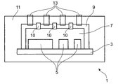
- FIG. 1 illustrates a cross section through an electronic device 1 according to an embodiment of the invention.
- the electronic device 1 may be a hand portable electronic device such as, for example, a portable radiotelephone, a personal digital assistant, a digital camera, etc.
- the electronic device 1 comprises a printed circuit board (PCB) 3 upon which a plurality of electronic components 5 are mounted.
- the PCB 3 may also comprise regions upon which no electronic components or circuitry are mounted. These regions can be used to handle the PCB 3 during the process of assembling the device 1 . For example, the regions may be used to hold the PCB 3 in position in a mold during injection molding.
- the electronic components 5 may, for example, comprise a processor module, an LCD display module or any other electronic component required for the electronic device 1 .
- the electromagnetic shield 9 encloses the electronic components 5 and protects them from electromagnetic interference which may come from other electronic components.
- the electromagnetic shield 9 comprises a plurality of holes 10 in the top of the shield 9 .
- the electromagnetic shield 9 may comprise a single hole through which the protective layer 7 can be formed.
- the shield 9 is made of a material which is electrically conductive but mechanically rigid. Suitable materials include stainless steel or nickel silver.
- the electronic device 1 also comprises a protective layer 7 which overlays and is in contact with the electronic components 5 .
- the protective layer is contained within the electromagnetic shield 9 .
- the protective layer 7 is electrically insulating.
- the protective layer 7 may also be thermally conductive.
- the protective layer 7 may be made of any material that has a good thermal conductivity but is electrically insulating.
- the protective layer may be made of material having a coefficient of thermal conductivity greater than 1 W/mK but is electrically insulating so as to avoid any short circuits being created.
- the precise properties required may depend on a number of factors including the sensitivity of the electronic components 5 and the thickness of the protective layer 7 .
- Suitable materials include, for example, resins such as ceramic or epoxy resins, urethane, silicone or composites of any such materials.
- the protective layer 7 may comprise an aluminium nitride (AlN) ceramic filler in an epoxy matrix. This has a coefficient of thermal conductivity of 1.7 W/mK and is electrically insulating
- the protective layer 7 overlays the entirety of the electronic components 5 .
- the protective layer may only cover a part of the components 5 .
- an electronic component 5 may have a first portion which is more perceptible to damage than a second portion in which case it may only be necessary to have the protective layer 7 overlaying the first portion.
- the protective layer 7 may overlay only some of the components. For example, it may only be necessary to have the protective layer 7 covering the most sensitive components.
- the electronic device 1 also comprises a layer 11 of injection molded material which overlays the electronic components 5 and the protective layer 7 .
- the injection molded material also overlays and is in contact with the electromagnetic shield 9 .
- the injection molded material may comprise a plastic or any other material which can be injection molded.
- the injection molded layer surrounds the entire cross section of the PCB 3 .
- the layer may only surround a portion of the PCB 3 , for example, the layer may only cover the side of the PCB 3 which has the electronic components 5 mounted on it.
- the layer 11 of injection molded material comprises a plurality of holes 13 .
- the plurality of holes 13 reduce the likelihood of the electronic components 5 overheating during operation of the device 1 .
- the layer 11 of injection molded material forms a cover for the electronic device 1 .
- the layer 11 may be waterproof and resistant to mechanical shocks so as to protect the electronic components 5 from environmental damage.
- the layer 11 of injection molded material may form the external cover of the device 1 .
- the electronic device 1 may be part of a further electronic device and be housed within a further casing.
- the further casing may act to provide further protection for the electronic device 1 .
- FIG. 2 illustrates a method of assembling an electronic device 1 according to a first embodiment of the invention.
- the electromagnetic shield 9 is mounted on the PCB 3 around the electronic components 5 .
- the electromagnetic shield 9 is mounted to the PCB 3 so as to form a continuous seal between the PCB 3 and the shield 9 thereby preventing leakage of the protective layer 7 during the assembly of the electronic device 1 .
- the shield 9 may be soldered to the PCB 3 .
- the protective layer 7 is formed, at step 23 , by injecting a liquid into the enclosure formed by the shield 9 over the electronic components 5 .
- the liquid may be injected though the holes 10 in the shield 9 .
- the liquid from which the protective layer 7 is formed has a high viscosity to ensure that it covers and attaches to all components 5 within the enclosure.
- the liquid from which the protective layer 7 is formed may be added at lower temperatures and with less force than required for injection molding so as to avoid damaging the electronic components 5 .
- the liquid is hardened to form a solid protective layer 7 .
- the liquid may be hardened by any suitable process for example, where the protective layer 7 comprises a ceramic resin the resin may be cured by heating.
- the layer may be thermally conductive so as to prevent the electronic components 5 overheating. Alternatively the temperatures required for curing may be much lower than those required for injection molding and may not damage the electronic components 5 .
- the protective layer 7 may be cured by a different process, such as, UV curing or two-component thermosetting.
- the PCB 3 is positioned in a mold, at step 27 , then, at step 29 , a cover of the electronic device 1 is formed by injection molding a layer 11 over the electronic components 5 and the protective layer 7 .
- the electronic components 5 are protected from damage during the injection molding step 29 by the protective layer 7 .
- the protective layer is thermally conductive, thus when the hot injection molded material makes thermal contact with the protective layer 7 the heat is dispersed through the layer thereby protecting the electronic components 5 from thermal shocks and localized hot spots which may damage sensitive components 5 .
- the protective layer 7 may also absorb the impact of the material during injection molding thereby protecting the components 5 from mechanical as well as thermal shocks.
- the injection molded layer 11 can be formed much closer to the components 5 than in prior art devices.
- the injection molded layer 11 is formed overlaying and in direct contact with the electromagnetic shield 9 . As the separation between the electronic components 5 and the injection molded layer 11 is reduced, this reduces the overall thickness of the electronic device 1 .
- the protective layer 7 may also prevent the electronic components 5 from overheating in use as heat generated by the component 5 will be conducted away from the component 5 .
- FIG. 3 illustrates a cross section through an electronic device 1 according to a second embodiment of the invention.
- the electronic device 1 comprises a PCB 3 , a plurality of electronic components 5 and an electromagnetic shield 9 mounted on the PCB 3 , a protective layer 7 overlaying the electronic components 5 and a layer of injection molded material 11 .
- the electronic device 1 also comprises a rigid substrate 15 upon which the PCB 3 is mounted.
- FIG. 4 illustrates the method steps of manufacturing an electronic device 1 according to the second embodiment of the invention.
- the PCB 3 is mounted on the rigid substrate 15 at step 31 .
- the PCB 3 may be mounted to the substrate 15 by any suitable means.
- the PCB 3 could be adhered to the substrate using a suitable adhesive such as glue or double sided tape.
- the PCB may be mounted to the substrate 15 using mechanical means such as screws or a snap-fit mechanism.
- the substrate 15 may be shaped so as to minimize the thickness and weight of the substrate 15 but still provide a strong support for the PCB 3 .
- the substrate 15 may be an I or U shaped beam.
- the substrate 15 may also be thermally conductive and may act as a heat sink for the electronic components 5 .
- the substrate 15 may be made from a material such as aluminium, stainless steel, magnesium, titanium or a composite of such materials.
- the shield 9 is mounted to the PCB 3 and at steps 35 and 37 the protective layer 7 is formed by injecting 33 the liquid over the components 5 and the hardening 35 the liquid.
- Steps 33 to 37 are analogous to steps 21 to 25 of the first embodiment.
- the PCB 3 is mounted 31 on the substrate 15 before the shield 9 is mounted 33 on the PCB 3 and before the protective layer 7 is formed 35 .
- the PCB 3 may be mounted on the substrate 15 after the shield 9 is mounted to the PCB 3 or even after the protective layer 7 has been formed.
- the PCB 3 and the substrate 15 are located in a mold and then at step 41 the injection molded layer 11 is formed over the PCB 3 and the substrate 15 thus the substrate 15 forms part of the mechanical structure electronic device 1 .
- the substrate 15 provides a mechanical support to the PCB 3 and electronic components 5 during injection molding 39 . Also, in embodiments where the substrate 15 is thermally conductive the substrate 15 acts as a heat sink and prevents the components from overheating during injection molding and in use.
- FIG. 5 illustrates an electronic device 1 according to a third embodiment of the invention.
- the electronic device 1 comprises a PCB 3 , a plurality of electronic components 5 and an electromagnetic shield 9 mounted on the PCB 3 , a protective layer 7 overlaying the electronic components 5 and a layer of injection molded material 11 .
- the device 1 also comprises a frame 51 which is mounted on the PCB in between the electronic components 5 .
- the protective layer 7 is formed over the electronic components 5 and the frame 51 .
- the frame 51 may provide some protection to the electronic components during the assembly of the device 1 .
- the frame 51 may act to absorb some of the pressure and/or heat during the formation of the injection molded layer 11 .
- the frame 51 may be made of any material having suitable properties to absorb heat and/or provide protection from the pressure.
- the frame 51 may be made of any material such as metal, ceramic, plastics or silicone etc.
- the frame may be made of Kevlar or carbon fiber.
- the dimensions of the frame 51 may depend on a number of factors including the sensitivity of the electronic components 5 , the material from which the frame 51 is made and the injection molding conditions, i.e. the temperature of the molten material when it is injected into the mold, and the force with which the molten material enters the mold.
- the frame 51 extends further from the PCB 3 than any of the electronic components 5 . In other embodiments the frame may extend for the same distance as the electronic components 5 or less than the electronic components 5 .
- the frame 51 is narrower than the gap between the electronic components 5 .
- the frame 51 may be as wide as the gap between electronic components 5 so that it fills the gap between them.
- the frame 51 is electronically insulating so as to prevent any short circuits being created between the electronic components 5 .
- the frame may be attached to the PCB 3 by any suitable means.
- the frame may be adhered to the PCB 3 using an adhesive, or the frame 51 may be soldered to the PCB 3 .
- the means used to mount the frame 51 to the PCB 3 may depend on the material used for the frame 51 .
- the frame 51 may surround all of the electronic components 5 or just a selection of the electronic components 5 . In some embodiments the frame 51 may extend around the entire perimeter of the electronic components 5 while in other embodiments the frame 51 may extend around only a section of the perimeter of the electronic components 5 .
- the electromagnetic shield 9 acts as a frame and contains the viscous material during formation of the protective layer 7 .
- the electronic components 5 may not require an electromagnetic shield 9 .
- a removable frame may be attached to the PCB 3 enclosing the electronic components 5 before the viscous material is injected over the components 5 .
- the removable frame ensures that only the components intended to be covered are covered.
- the removable frame would then be detached from the PCB 3 before the injection molding step 27 .
- the removable frame may be attached to the PCB 3 by any suitable method which forms a seal between the PCB 3 and the frame and prevents leakage of the protective layer 7 during assembly of the electronic device 1 but allows the frame to be removed once the protective layer 7 has been formed.
- the PCB may be placed in a pressurized container during the formation of the protective layer 7 so that a hermetic seal is created between the frame and the PCB.
- the injection molded layer 11 may overlay and be in direct contact with the protective layer 7 .
- the protective layer 7 may be thermally insulating. In such embodiments the protective layer 7 will protect the electronic components 5 from the heat of the injection molding process. A thermally insulating protective layer 7 may also protect the electronic components from overheating during hardening of the layer 7 by heat curing.
- the PCB 3 may be thermally conductive or may comprise a heat sink to prevent the electronic components 5 from overheating in use.
- pressurized gas may be added to the injection molding material during the injection molding step 29 , 41 . This allows for the formation of 3D patterns on the surface of the injection molded layer 11 .
- the electronic components 5 are only mounted on one side of the PCB 3 . In other embodiments there may be electronic components 5 mounted on both sides of the PCB 3 . Some or all of the electronic components 5 may be covered by a protective layer 7 and injection molded layer 11 as described above.
- the injection molded layer 11 comprises a plurality of holes 13 . In other embodiments there may be no holes in the layer 13 . For example, in some embodiments these holes may not be necessary for ventilation or, if the injection molded layer is the outer cover of the device 1 it may be considered more aesthetic not to have any holes.
- the protective layer may be formed from a pre-molded layer which is then attached to the PCB.
Abstract
Description
Claims (20)
Priority Applications (4)
| Application Number | Priority Date | Filing Date | Title |
|---|---|---|---|
| US11/647,613 US7742309B2 (en) | 2006-12-29 | 2006-12-29 | Electronic device and method of assembling an electronic device |
| CN2007800483325A CN101569249B (en) | 2006-12-29 | 2007-12-13 | An electronic device and method of assembling an electronic device |
| PCT/EP2007/010938 WO2008080533A1 (en) | 2006-12-29 | 2007-12-13 | An electronic device and method of assembling an electronic device |
| EP07856684A EP2098104A1 (en) | 2006-12-29 | 2007-12-13 | An electronic device and method of assembling an electronic device |
Applications Claiming Priority (1)
| Application Number | Priority Date | Filing Date | Title |
|---|---|---|---|
| US11/647,613 US7742309B2 (en) | 2006-12-29 | 2006-12-29 | Electronic device and method of assembling an electronic device |
Publications (2)
| Publication Number | Publication Date |
|---|---|
| US20080158825A1 US20080158825A1 (en) | 2008-07-03 |
| US7742309B2 true US7742309B2 (en) | 2010-06-22 |
Family
ID=39327135
Family Applications (1)
| Application Number | Title | Priority Date | Filing Date |
|---|---|---|---|
| US11/647,613 Active US7742309B2 (en) | 2006-12-29 | 2006-12-29 | Electronic device and method of assembling an electronic device |
Country Status (4)
| Country | Link |
|---|---|
| US (1) | US7742309B2 (en) |
| EP (1) | EP2098104A1 (en) |
| CN (1) | CN101569249B (en) |
| WO (1) | WO2008080533A1 (en) |
Cited By (1)
| Publication number | Priority date | Publication date | Assignee | Title |
|---|---|---|---|---|
| US20160192499A1 (en) * | 2014-12-26 | 2016-06-30 | Htc Corporation | Electronic device and manufacturing method thereof |
Families Citing this family (6)
| Publication number | Priority date | Publication date | Assignee | Title |
|---|---|---|---|---|
| TWI355220B (en) * | 2008-07-14 | 2011-12-21 | Unimicron Technology Corp | Circuit board structure |
| DE202010018233U1 (en) * | 2010-08-08 | 2015-01-21 | Ssb Wind Systems Gmbh & Co. Kg | Electric device |
| CN102647863A (en) * | 2012-04-10 | 2012-08-22 | 苏州达方电子有限公司 | Electronic device |
| DE102015118498A1 (en) * | 2015-10-29 | 2017-05-04 | Endress+Hauser Conducta Gmbh+Co. Kg | Method for casting a printed circuit board with components |
| DE102017208076A1 (en) * | 2017-05-12 | 2018-11-15 | Magna Powertrain Bad Homburg GmbH | Component with EMC protection for electronic board |
| CN107195600A (en) * | 2017-06-20 | 2017-09-22 | 广东美的制冷设备有限公司 | Chip-packaging structure |
Citations (14)
| Publication number | Priority date | Publication date | Assignee | Title |
|---|---|---|---|---|
| US4855868A (en) * | 1987-01-20 | 1989-08-08 | Harding Ade Yemi S K | Preformed packaging arrangement for energy dissipating devices |
| US5285104A (en) * | 1991-10-02 | 1994-02-08 | Ibiden Co., Ltd. | Encapsulated semiconductor device with bridge sealed lead frame |
| EP1065916A2 (en) | 1999-06-28 | 2001-01-03 | Hitachi, Ltd. | Resin sealed electronic device |
| US6191360B1 (en) * | 1999-04-26 | 2001-02-20 | Advanced Semiconductor Engineering, Inc. | Thermally enhanced BGA package |
| US20030019647A1 (en) | 2001-07-25 | 2003-01-30 | Luettgen Michael John | Protected electronic assembly |
| US6768654B2 (en) * | 2000-09-18 | 2004-07-27 | Wavezero, Inc. | Multi-layered structures and methods for manufacturing the multi-layered structures |
| US6849800B2 (en) * | 2001-03-19 | 2005-02-01 | Hewlett-Packard Development Company, L.P. | Board-level conformal EMI shield having an electrically-conductive polymer coating over a thermally-conductive dielectric coating |
| US20060003137A1 (en) * | 2004-07-02 | 2006-01-05 | Amstutz Aaron K | System and method for encapsulation and protection of components |
| US20060018098A1 (en) | 2004-07-22 | 2006-01-26 | Adrian Hill | PCB board incorporating thermo-encapsulant for providing controlled heat dissipation and electromagnetic functions and associated method of manufacturing a PCB board |
| WO2006017484A1 (en) | 2004-08-06 | 2006-02-16 | Hitek Power Corporation | Selective encapsulation of electronic components |
| GB2418539A (en) | 2004-09-23 | 2006-03-29 | Vetco Gray Controls Ltd | Electrical circuit package |
| US20060170092A1 (en) * | 2005-02-01 | 2006-08-03 | Stats Chippac Ltd. | Semiconductor package system with cavity substrate |
| US20060221591A1 (en) | 2005-04-05 | 2006-10-05 | Hon Hai Precision Industry Co., Ltd. | EMI shielding package and method for making the same |
| US20090004557A1 (en) * | 2007-06-26 | 2009-01-01 | Nokia Corporation | Protecting a functional component and a protected functional component |
-
2006
- 2006-12-29 US US11/647,613 patent/US7742309B2/en active Active
-
2007
- 2007-12-13 CN CN2007800483325A patent/CN101569249B/en not_active Expired - Fee Related
- 2007-12-13 EP EP07856684A patent/EP2098104A1/en not_active Withdrawn
- 2007-12-13 WO PCT/EP2007/010938 patent/WO2008080533A1/en active Application Filing
Patent Citations (16)
| Publication number | Priority date | Publication date | Assignee | Title |
|---|---|---|---|---|
| US4855868A (en) * | 1987-01-20 | 1989-08-08 | Harding Ade Yemi S K | Preformed packaging arrangement for energy dissipating devices |
| US5285104A (en) * | 1991-10-02 | 1994-02-08 | Ibiden Co., Ltd. | Encapsulated semiconductor device with bridge sealed lead frame |
| US6191360B1 (en) * | 1999-04-26 | 2001-02-20 | Advanced Semiconductor Engineering, Inc. | Thermally enhanced BGA package |
| EP1065916A2 (en) | 1999-06-28 | 2001-01-03 | Hitachi, Ltd. | Resin sealed electronic device |
| US6768654B2 (en) * | 2000-09-18 | 2004-07-27 | Wavezero, Inc. | Multi-layered structures and methods for manufacturing the multi-layered structures |
| US6849800B2 (en) * | 2001-03-19 | 2005-02-01 | Hewlett-Packard Development Company, L.P. | Board-level conformal EMI shield having an electrically-conductive polymer coating over a thermally-conductive dielectric coating |
| US20030019647A1 (en) | 2001-07-25 | 2003-01-30 | Luettgen Michael John | Protected electronic assembly |
| US6683250B2 (en) * | 2001-07-25 | 2004-01-27 | Visteon Global Technologies, Inc. | Protected electronic assembly |
| US20060003137A1 (en) * | 2004-07-02 | 2006-01-05 | Amstutz Aaron K | System and method for encapsulation and protection of components |
| US20060018098A1 (en) | 2004-07-22 | 2006-01-26 | Adrian Hill | PCB board incorporating thermo-encapsulant for providing controlled heat dissipation and electromagnetic functions and associated method of manufacturing a PCB board |
| WO2006017484A1 (en) | 2004-08-06 | 2006-02-16 | Hitek Power Corporation | Selective encapsulation of electronic components |
| GB2418539A (en) | 2004-09-23 | 2006-03-29 | Vetco Gray Controls Ltd | Electrical circuit package |
| US20080080141A1 (en) * | 2004-09-23 | 2008-04-03 | Hans-Joachim Krokoszinski | Electrical Circuit Package |
| US20060170092A1 (en) * | 2005-02-01 | 2006-08-03 | Stats Chippac Ltd. | Semiconductor package system with cavity substrate |
| US20060221591A1 (en) | 2005-04-05 | 2006-10-05 | Hon Hai Precision Industry Co., Ltd. | EMI shielding package and method for making the same |
| US20090004557A1 (en) * | 2007-06-26 | 2009-01-01 | Nokia Corporation | Protecting a functional component and a protected functional component |
Cited By (1)
| Publication number | Priority date | Publication date | Assignee | Title |
|---|---|---|---|---|
| US20160192499A1 (en) * | 2014-12-26 | 2016-06-30 | Htc Corporation | Electronic device and manufacturing method thereof |
Also Published As
| Publication number | Publication date |
|---|---|
| CN101569249B (en) | 2012-05-23 |
| WO2008080533A1 (en) | 2008-07-10 |
| EP2098104A1 (en) | 2009-09-09 |
| CN101569249A (en) | 2009-10-28 |
| US20080158825A1 (en) | 2008-07-03 |
Similar Documents
| Publication | Publication Date | Title |
|---|---|---|
| US7742309B2 (en) | Electronic device and method of assembling an electronic device | |
| US7486517B2 (en) | Hand-held portable electronic device having a heat spreader | |
| JP4353186B2 (en) | Electronic equipment | |
| US9485870B2 (en) | Methods for transparent encapsulation and selective encapsulation | |
| US20050081377A1 (en) | Method for forming an electronic assembly | |
| US20100230155A1 (en) | Apparatus comprising an electronics module and method of assembling apparatus | |
| EP1357780A3 (en) | Camera module having a shield casing and a sealing mechanism | |
| US20150116958A1 (en) | Circuit board modules having mechanical features | |
| US8154876B2 (en) | Circuit board module and electronic apparatus | |
| CN110662372A (en) | Electronic unit and method for manufacturing the same | |
| US20120002381A1 (en) | Method for manufacturing a liquid-tight electronic device, and liquid-tight electronic device | |
| US20010045297A1 (en) | Molding of electrical devices with a thermally conductive and electrically insulative polymer composition | |
| US20100155111A1 (en) | Mounting structure | |
| KR101350482B1 (en) | Tact switch | |
| US20230309237A1 (en) | Packaging structure, lens module, and electronic device | |
| US10334733B2 (en) | Circuit structure | |
| US10849235B1 (en) | Method of manufacture of a structure and structure | |
| JP2009267313A (en) | Enclosure for electronic apparatus and method of manufacturing the same | |
| CN210298180U (en) | Electronic circuit board and electronic equipment | |
| US11197382B2 (en) | Electronic module for a transmission control unit, and transmission control unit | |
| CN117715333A (en) | Electronic device with display and camera window | |
| EP4340339A1 (en) | Electronic devices with displays and camera windows | |
| US20240121923A1 (en) | Thermal management system including an overmolded layer and a conductive layer over a circuit board | |
| JP2002134929A (en) | Electronic circuit board and electronic apparatus including the same | |
| JP2012004214A (en) | Flexible circuit board with waterproof member and method of manufacturing the same |
Legal Events
| Date | Code | Title | Description |
|---|---|---|---|
| AS | Assignment |
Owner name: NOKIA CORPORATION, FINLAND Free format text: ASSIGNMENT OF ASSIGNORS INTEREST;ASSIGNORS:HAKUNTI, JUSSI;KILPI, PEKKA;VANSKA, ANSSI;AND OTHERS;REEL/FRAME:019121/0401;SIGNING DATES FROM 20070208 TO 20070219 Owner name: NOKIA CORPORATION,FINLAND Free format text: ASSIGNMENT OF ASSIGNORS INTEREST;ASSIGNORS:HAKUNTI, JUSSI;KILPI, PEKKA;VANSKA, ANSSI;AND OTHERS;SIGNING DATES FROM 20070208 TO 20070219;REEL/FRAME:019121/0401 |
|
| FEPP | Fee payment procedure |
Free format text: PAYOR NUMBER ASSIGNED (ORIGINAL EVENT CODE: ASPN); ENTITY STATUS OF PATENT OWNER: LARGE ENTITY |
|
| STCF | Information on status: patent grant |
Free format text: PATENTED CASE |
|
| FPAY | Fee payment |
Year of fee payment: 4 |
|
| AS | Assignment |
Owner name: NOKIA TECHNOLOGIES OY, FINLAND Free format text: ASSIGNMENT OF ASSIGNORS INTEREST;ASSIGNOR:NOKIA CORPORATION;REEL/FRAME:035603/0543 Effective date: 20150116 |
|
| MAFP | Maintenance fee payment |
Free format text: PAYMENT OF MAINTENANCE FEE, 8TH YEAR, LARGE ENTITY (ORIGINAL EVENT CODE: M1552) Year of fee payment: 8 |
|
| MAFP | Maintenance fee payment |
Free format text: PAYMENT OF MAINTENANCE FEE, 12TH YEAR, LARGE ENTITY (ORIGINAL EVENT CODE: M1553); ENTITY STATUS OF PATENT OWNER: LARGE ENTITY Year of fee payment: 12 |