US7737534B2 - Semiconductor devices that include germanium nanofilm layer disposed within openings of silicon dioxide layer - Google Patents

Semiconductor devices that include germanium nanofilm layer disposed within openings of silicon dioxide layer Download PDF

Info

Publication number
US7737534B2
US7737534B2 US12/136,193 US13619308A US7737534B2 US 7737534 B2 US7737534 B2 US 7737534B2 US 13619308 A US13619308 A US 13619308A US 7737534 B2 US7737534 B2 US 7737534B2
Authority
US
United States
Prior art keywords
layer
germanium
nanofilm
intrinsic
semiconductor device
Prior art date
Legal status (The legal status is an assumption and is not a legal conclusion. Google has not performed a legal analysis and makes no representation as to the accuracy of the status listed.)
Active
Application number
US12/136,193
Other versions
US20090302426A1 (en
Inventor
Sean R. McLaughlin
Narsingh Bahadur Singh
Brian Wagner
Andre Berghmans
David J. Knuteson
David Kahler
Anthony A. Margarella
Current Assignee (The listed assignees may be inaccurate. Google has not performed a legal analysis and makes no representation or warranty as to the accuracy of the list.)
Northrop Grumman Systems Corp
Original Assignee
Northrop Grumman Systems Corp
Priority date (The priority date is an assumption and is not a legal conclusion. Google has not performed a legal analysis and makes no representation as to the accuracy of the date listed.)
Filing date
Publication date
Application filed by Northrop Grumman Systems Corp filed Critical Northrop Grumman Systems Corp
Priority to US12/136,193 priority Critical patent/US7737534B2/en
Assigned to NORTHROP GRUMMAN SYSTEMS CORPORATION reassignment NORTHROP GRUMMAN SYSTEMS CORPORATION ASSIGNMENT OF ASSIGNORS INTEREST (SEE DOCUMENT FOR DETAILS). Assignors: KAHLER, DAVID, MARGARELLA, ANTHONY A., WAGNER, BRIAN, BERGHMANS, ANDRE, KNUTESON, DAVID J., MCLAUGHLIN, SEAN R., SINGH, NARSHINGH BAHADUR
Priority to EP09162210.0A priority patent/EP2133534B1/en
Publication of US20090302426A1 publication Critical patent/US20090302426A1/en
Application granted granted Critical
Publication of US7737534B2 publication Critical patent/US7737534B2/en
Active legal-status Critical Current
Anticipated expiration legal-status Critical

Links

Images

Classifications

    • FMECHANICAL ENGINEERING; LIGHTING; HEATING; WEAPONS; BLASTING
    • F01MACHINES OR ENGINES IN GENERAL; ENGINE PLANTS IN GENERAL; STEAM ENGINES
    • F01PCOOLING OF MACHINES OR ENGINES IN GENERAL; COOLING OF INTERNAL-COMBUSTION ENGINES
    • F01P3/00Liquid cooling
    • F01P3/22Liquid cooling characterised by evaporation and condensation of coolant in closed cycles; characterised by the coolant reaching higher temperatures than normal atmospheric boiling-point
    • F01P3/2285Closed cycles with condenser and feed pump
    • FMECHANICAL ENGINEERING; LIGHTING; HEATING; WEAPONS; BLASTING
    • F01MACHINES OR ENGINES IN GENERAL; ENGINE PLANTS IN GENERAL; STEAM ENGINES
    • F01PCOOLING OF MACHINES OR ENGINES IN GENERAL; COOLING OF INTERNAL-COMBUSTION ENGINES
    • F01P2025/00Measuring
    • F01P2025/04Pressure
    • YGENERAL TAGGING OF NEW TECHNOLOGICAL DEVELOPMENTS; GENERAL TAGGING OF CROSS-SECTIONAL TECHNOLOGIES SPANNING OVER SEVERAL SECTIONS OF THE IPC; TECHNICAL SUBJECTS COVERED BY FORMER USPC CROSS-REFERENCE ART COLLECTIONS [XRACs] AND DIGESTS
    • Y10TECHNICAL SUBJECTS COVERED BY FORMER USPC
    • Y10STECHNICAL SUBJECTS COVERED BY FORMER USPC CROSS-REFERENCE ART COLLECTIONS [XRACs] AND DIGESTS
    • Y10S977/00Nanotechnology
    • Y10S977/70Nanostructure
    • Y10S977/773Nanoparticle, i.e. structure having three dimensions of 100 nm or less
    • Y10S977/774Exhibiting three-dimensional carrier confinement, e.g. quantum dots

Definitions

  • Embodiments of the present invention relate generally to semiconductor devices and their methods of manufacture, and in particular to semiconductor devices having germanium layers incorporated therein.
  • Silicon and germanium are commonly used in such electronic devices.
  • silicon is the most widely used material in semiconductor devices due to its low cost, relatively simple processing, and useful temperature range.
  • the electronic properties and behavior of silicon and germanium can be relatively easily controlled by the addition of doping elements, for example, in the manufacture of P-I-N and N-I-P diodes.
  • Recent research has focused on making devices in which a layer of germanium is deposited over the entire surface of a silicon wafer.
  • dislocations can occur due to lattice mismatches between the silicon and germanium layers.
  • the electronic properties of such devices have been less than desired.
  • the present invention is directed to a process of fabricating a semiconductor device having a germanium nanofilm layer that is selectively deposited on a silicon substrate in discrete regions or patterns.
  • this embodiment of the invention provides a semiconductor device having germanium film layer that is disposed in desired regions having a desired patterns that can be prepared in the absence of etching and patterning the germanium film layer.
  • the present invention also provides for a process for preparing a semiconductor device having a silicon substrate having one conductivity type and a germanium nanofilm layer of a different conductivity type.
  • This embodiment of the invention also provides for semiconductor devices having selectively grown germanium nanofilm layer, such as diodes including light emitting diodes, photodetectors, and like.
  • Embodiments of the present invention can also be used to make advanced semiconductor devices such as CMOS devices, MOSFET devices, and the like.
  • the present invention provides a process of selectively depositing a germanium nanofilm layer on a silicon substrate in which a layer of SiO 2 is formed on the substrate followed by etching one or more openings, such as trenches, in the SiO 2 layer to expose select regions of the silicon substrate.
  • a germanium nanofilm layer is epitaxially deposited on the exposed regions of the silicon substrate so that at least a portion of the germanium nanofilm layer is in direct physical contact with the silicon substrate.
  • the germanium nanofilm layer is formed by depositing a plurality of tightly and closely spaced nanodots on the exposed silicon substrate surface to form a continuous film-like structure.
  • the germanium nanofilm layer as well as a layer from which the SiO 2 layer is formed, can be deposited utilizing a variety of different techniques including Metal Organic Vapor Phase epitaxy processes (MO-CVD), molecular beam epitaxial processes (MBE) chemical vapor deposition (CVD), physical vapor deposition (PVD) and other thin film deposition processes.
  • MO-CVD Metal Organic Vapor Phase epitaxy processes
  • MBE molecular beam epitaxial processes
  • CVD chemical vapor deposition
  • PVD physical vapor deposition
  • the openings in the SiO 2 layer can be made using photolithography techniques, such as plasma dry etch or hydrofluoric acid wet etch.
  • the number of openings, thickness of the openings, and the pattern of the openings can be selected based on the desired semiconductor device and its intended application.
  • the present invention can be used to prepare semiconductor devices in which an intrinsic layer, such as an intrinsic silicon layer or intrinsic germanium layer is disposed between the germanium nanofilm layer and the silicon substrate.
  • an intrinsic layer such as an intrinsic silicon layer or intrinsic germanium layer is disposed between the germanium nanofilm layer and the silicon substrate.
  • an intrinsic silicon layer can be deposited on the surface of the silicon substrate.
  • a portion of the intrinsic silicon layer can then be oxidized to form the SiO 2 layer.
  • the SiO 2 layer can then be patterned and etched to form one or more openings in which a surface of the intrinsic layer is exposed.
  • the germanium nanofilm layer can then be epitaxially deposited onto the exposed surface of the intrinsic silicon layer.
  • the present invention provides a semiconductor device having a silicon substrate of a first conductivity-type; an intrinsic layer formed on the substrate, a silicon dioxide layer formed on an outer portion of the intrinsic layer having one or more openings formed therein in which select portions of the surface of the intrinsic layer are exposed, and a germanium nanofilm layer of a second conductivity type disposed in the openings and in direct physical contact with the intrinsic layer.
  • metal contact layers may be formed on opposite sides of the semiconductor device. Suitable materials for the contact layers include gold, copper, and aluminum.
  • the present invention provides a semiconductor device in which an intrinsic germanium nanofilm layer is deposited in direct physical contact with at least a portion of the surface of the silicon substrate.
  • the surface of the silicon substrate can be exposed by etching one or more openings in an SiO 2 layer that is disposed above the intrinsic germanium nanofilm layer.
  • a second silicon layer having a different conductivity than the silicon substrate is then deposited in the opening on at least a portion of the surface of the intrinsic germanium nanofilm layer.
  • the present invention provides a semiconductor device in which an intrinsic germanium nanofilm layer is deposited in direct physical contact with at least a portion of the surface of silicon substrate and a second germanium nanofilm layer having a different conductivity than the silicon substrate is deposited in the opening on the intrinsic germanium nanofilm layer.
  • the intrinsic silicon layer can be deposited with epitaxy processes as discussed above.
  • embodiments of the present invention provide a method of selectively depositing a nanofilm layer of germanium of a silicon substrate.
  • the present invention can be used to fabricate a wide variety of different semiconductor devices.
  • FIG. 1 is a schematic illustration depicting a process of forming a germanium nanofilm layer on a silicon substrate
  • FIG. 2 is a schematic illustration depicting a process of forming a semiconductor device having a silicon substrate of a first conductivity type and a germanium nanofilm layer of a second conductivity type selectively deposited on an intrinsic silicon layer;
  • FIG. 3 is a cross-section of a semiconductor device having a silicon substrate of a first conductivity type and germanium nanofilm layer of a second conductivity type that is selectively deposited on a surface of an intrinsic silicon layer in openings formed in an SiO 2 layer;
  • FIG. 4 is a cross-section of a semiconductor device having a silicon substrate of a first conductivity type and a silicon layer of a second conductivity type, wherein the silicon layer is deposited on an intrinsic germanium nanofilm layer that is selectively deposited on a surface of silicon substrate in openings formed in an SiO 2 layer;
  • FIG. 5 is a cross-section of a semiconductor device having a silicon substrate of a first conductivity type, a germanium nanofilm layer of a second conductivity type, and an intrinsic germanium nanofilm layer wherein germanium nanofilm layers are selectively deposited formed in an SiO 2 layer;
  • FIG. 6 is an SEM image of a silicon substrate having an outer SiO 2 layer with openings formed therein and in which a nanofilm layer of germanium has selectively been deposited in the openings on the surface of the silicon substrate;
  • FIG. 7 is an SEM image of PIN diode that has been fabricated in accordance with the invention.
  • FIG. 8 is a cross-sectional FIB image of the PIN diode of FIG. 7 ;
  • FIG. 9 is a I-V curve for a P-I-N diode that is in accordance with one embodiment of the invention.
  • FIG. 10 is a I-V curve continuous sweep test for a P-I-N diode that is in accordance with one embodiment of the invention.
  • a process of selectively depositing a germanium nanofilm layer on a silicon substrate is schematically illustrated.
  • a silicon substrate is provided.
  • Block 10 A layer of silicon dioxide (SiO 2 ) is then formed on the substrate.
  • Block 12 The SiO 2 layer is then etched using photolithography techniques to produce one or more openings in the SiO 2 layer to expose select regions of the surface of the silicon substrate. In one embodiment, the openings define openings that extend through the thickness of the SiO 2 layer to thereby expose select regions of an underlying layer.
  • Block 14 A germanium nanofilm layer is then epitaxially grown within the openings so that the germanium nanofilm layer is in direct physical contact with the silicon layer. Block 16 .
  • the germanium nanofilm layer is selectively deposited in the openings with little to none of the germanium being deposited on the SiO 2 layer.
  • the germanium nanofilm layer is limited to being present in the one or more openings formed in the SiO 2 layer with no germanium being deposited on the surface of the SiO 2 layer.
  • the germanium nanofilm layer desirably has a thickness ranging from about 10 to 5,000 nanometers (nm), and more desirably from about 100 to 1,000 nm.
  • the germanium nanofilm layer is formed by depositing a plurality of tightly and closely spaced nanodots on the exposed silicon substrate surface. Ideally, the spacing of the germanium nanodots is such that the nanodots coalesce to have a continuous film-like structure.
  • the initial deposition of the germanium nanodots is such that the spacing between adjacent dots is no more than 1 nm, and more typically no more than 10 nm.
  • each nanodot can have a height or thickness of approximately 5 nm-50 nm and a diameter on the order of approximately 5 nm. It should be recognized that the dimensions of the nanodots can be adapted in accordance with the requirements of the particular application and device being fabricated. For example, wavelength of emission can be matched to a waveguide and/or detector for optical signal transmission.
  • the germanium nanodoats can be deposited at temperatures ranging from about 450° C. to 1000° C., and at pressures from about 10 to 760 Torr, with a pressure of about 20 Torr being somewhat preferred.
  • the deposition of the germanium nanodots is carried out a temperature from about 450 to 930° C. and at a pressure from about 10 to 60 torr.
  • the coalescing of the germanium nanodots is due to high energy surfaces, especially surfaces which have been etched. As the nanodots initially grow, the nanodots tend to initiate at these high energy surfaces as oppose to low energy surfaces, such as unetched silicon. As the nanodots continue to grow, in close proximity to each other, the nanodots touch and fuse by overcoming the lattice mismatch between germanium and silicon. It is believed that the lattice mismatch between germanium and silicon is a significant factor in the initial growth of germanium as a nanodot.
  • the germanium nanofilm layer as well as a layer from which the SiO 2 layer is formed, can be deposited utilizing a variety of different techniques including Metal Organic Vapor Phase epitaxy processes (MO-CVD), molecular beam epitaxial processes (MBE) chemical vapor deposition (CVD), physical vapor deposition (PVD) and other thin film deposition processes.
  • MO-CVD Metal Organic Vapor Phase epitaxy processes
  • MBE molecular beam epitaxial processes
  • CVD chemical vapor deposition
  • PVD physical vapor deposition
  • the openings in the SiO 2 layer can be made using photolithography techniques, such as plasma dry etch or hydrofluoric acid wet etch.
  • the number of openings, thickness of the openings, and the pattern of the openings can be selected based on the desired semiconductor device and its intended application.
  • the SiO 2 layer can be etched to have a desired pattern so that the resulting germanium nanofilm layer also has a desired pattern.
  • semiconductor devices can be fabricated having a germanium nanofilm layer with a desired pattern without the need to pattern and etch a germanium film layer.
  • the present invention can be used to prepare semiconductor devices in which an intrinsic layer, such as an intrinsic silicon layer or intrinsic germanium layer is disposed between the germanium nanofilm layer and the silicon substrate.
  • an intrinsic layer such as an intrinsic silicon layer or intrinsic germanium layer is disposed between the germanium nanofilm layer and the silicon substrate.
  • an intrinsic silicon layer can be deposited on the surface of the silicon substrate.
  • the intrinsic silicon layer can be deposited with epitaxy processes as discussed above.
  • a portion of the intrinsic silicon layer can be oxidized to form the SiO 2 layer.
  • the SiO 2 layer can then be patterned and etched to form one or more openings in which a surface of the intrinsic layer is exposed.
  • the germanium nanofilm layer can then be epitaxially deposited onto the exposed surface of the intrinsic silicon layer.
  • this embodiment of the present invention can be used to fabricate P-I-N type or N-I-P type diodes, among other types of semiconductor devices.
  • a semiconductor device can be fabricated in which the silicon substrate has a P-type conductivity, such as P, P+, P++, etc., and the germanium nanofilm layer has a N-type conductivity, such as N, N +, N ++, etc.
  • the silicon substrate can have an N-type conductivity, such as, N, N +, N ++ etc.
  • the germanium nanofilm layer can have a P-type conductivity, such as P, P+, P++, etc.
  • Exemplary N-type doping materials include phosphorus, arsenic, and antimony.
  • Exemplary P-type doping materials include boron and aluminum.
  • the silicon layer and the germanium nanofilm layer can be doped with N- or P-type material using methods known in the art.
  • a process of preparing a semiconductor device in accordance with one embodiment of the present invention is schematically illustrated.
  • a silicon substrate of a first conductivity is provided.
  • Block 20 a layer of silicon is deposited onto the surface of the silicon substrate.
  • Block 22 An outer portion of the silicon layer is then oxidized to form a SiO 2 layer and an intrinsic silicon layer on the silicon substrate.
  • Block 24 The intrinsic silicon layer is disposed between the silicon substrate and the outer SiO 2 layer.
  • the SiO 2 layer is then etched using photolithography techniques to produce one or more openings in the SiO 2 layer to expose select regions of the surface of the intrinsic silicon layer.
  • Block 26 A germanium nanofilm layer of a second conductivity type is then epitaxially grown within the openings so that the germanium nanofilm layer is in direct physical contact with the intrinsic silicon layer.
  • Block 28 .
  • each layer of the semiconductor device e.g., SiO 2 layer, intrinsic silicon layer, germanium nanofilm layer, etc.
  • the semiconductor device e.g., SiO 2 layer, intrinsic silicon layer, germanium nanofilm layer, etc.
  • each layer of the semiconductor device is disposed on a preceding layer so that the layers are positionally on or over another layer regardless of whether there are any intervening layers. For example, if one layer is positioned on another layer, this does not necessarily mean that the two layers are in physical contact with each other.
  • the semiconductor devices comprise diodes of the P-I-N type. It should be understood that an N-I-P device can also be fabricated and operate in accordance with the present invention. Selection of device type depends on the particular application in which the device is being used.
  • FIG. 3 a semiconductor device 30 is illustrated in which the device includes a silicon substrate 32 of a first conductivity-type; an intrinsic layer 34 , a silicon dioxide layer 36 having one or more openings 38 formed therein, and a germanium nanofilm layer 40 of a second conductivity type disposed in the openings and in direct physical contact with the surface 42 intrinsic layer.
  • a silicon substrate 32 that has been doped with either a P- or N-type semiconductor material is provided.
  • An intrinsic silicon layer 34 is then deposited on the silicon substrate 32 using MOCVD epitaxy.
  • the thickness of the intrinsic silicon layer 34 can range from between about 20 to 400 nm.
  • the intrinsic silicon layer can have a thickness from about 20 to 100 nm.
  • An outer portion of the intrinsic silicon layer 34 is oxidized to form SiO 2 layer 36 .
  • the intrinsic silicon layer can be oxidized, for example, using a dry oxygen or wet oxygen environment under high temperature to grow the SiO 2 layer.
  • the oxidation of the intrinsic silicon layer is carried out at a temperature from about 800 to 1,200 C, and more typically from about 850 to 1,000 C.
  • the thickness of the SiO 2 layer can be selected based on a desired and/or expected thickness of the germanium nanofilm layer 40 .
  • the thickness of the SiO 2 layer is between about 10 to 100 nm, and more typically between about 50 and 100 nm.
  • a photolithography mask can be used to pattern and etch the SiO 2 layer to form one or more openings in the SiO 2 layer.
  • the SiO 2 layer is desirably etched to expose at least a portion of the surface of the intrinsic silicon layer.
  • the germanium nanofilm layer 40 is then grown in the openings using a deposition process, such as MOCVD.
  • the germanium nanofilm layer is created in the opening(s) by depositing a plurality of tightly packed nanodots that coalesce to create a continuous germanium nanofilm layer in each of the openings.
  • the germanium nanofilm layer is desirably a different conductivity type than the silicon substrate.
  • metal contact layers 44 , 46 are formed on opposite sides of the semiconductor device 30 .
  • Suitable materials for the contact layers include gold, copper, and aluminum.
  • the contact layers can be formed using deposition processes discussed above, such as PVD (physical vapor deposition).
  • the thickness of the contact layers generally ranges between about 50 to 5,000 nm.
  • metal evaporation such as e-beam or resistance heated, can also be used to form the contact layers.
  • FIG. 4 illustrates an embodiment of a semiconductor device 30 a in which an intrinsic germanium nanofilm layer 48 is deposited in direct physical contact with at least a portion of the surface 54 of the silicon substrate 32 .
  • the surface 54 of the silicon substrate 32 is exposed by etching one or more openings in the SiO 2 layer 36 as discussed above.
  • a second silicon layer 50 having a different conductivity than the silicon substrate is then deposited in the opening on at least a portion of the surface 56 of the intrinsic germanium nanofilm layer 48 .
  • the silicon substrate 32 can have a conductivity of the P-type whereas the second silicon layer 50 has a conductivity of the N-type, and vice versa.
  • the SiO 2 layer 36 can be formed directly on the surface 54 of the silicon substrate, and can then be etched to expose a portion of the surface 54 of the silicon substrate.
  • the intrinsic germanium nanofilm layer 48 is then deposited within the opening 38 in direct physical contact with the thus exposed surface 54 of the silicon substrate.
  • the intrinsic germanium nanofilm layer has a thickness between about 5 to 50 nm, and more typically between about 10 to 30 nm
  • the second silicon layer 50 has a thickness between about 10 to 100 nm, and more typically between about 25 to 75 nm.
  • the thickness of the intrinsic germanium nanofilm layer 50 is between about 10 to 50% of the total depth of the opening.
  • Contacts 44 , 46 can then be formed on opposite sides of the semiconductor device 20 a as discussed above.
  • the present invention provides a semiconductor device having an intrinsic silicon layer with a thickness that ranges from about 10 to 100 nm, and a germanium nanofilm layer having a thickness ranging from about 25 to 250 nm.
  • FIG. 5 illustrates a further embodiment of a semiconductor device 30 b in which an intrinsic germanium nanofilm layer 48 is deposited in direct physical contact with at least a portion of the surface 54 of silicon substrate 32 .
  • a second germanium nanofilm layer 40 having a different conductivity than the silicon substrate 32 is deposited in the opening on the intrinsic germanium nanofilm layer.
  • the silicon substrate 32 can have a conductivity of the P-type whereas the second germanium nanofilm layer 40 has a conductivity of the N-type, and vice versa.
  • the SiO 2 layer 36 can be formed directly on the surface 54 of the silicon substrate, and can then be etched to expose a portion of the surface of the silicon substrate.
  • the intrinsic germanium nanofilm layer can then be deposited within the opening in direct physical contact with the thus exposed surface of the silicon substrate as discussed above in connection with FIG. 4 .
  • the second germanium nanofilm layer is then deposited in the opening 38 on the surface 56 of the intrinsic germanium nanofilm layer as discussed above.
  • Contacts 44 , 46 can then be formed on opposite sides of the semiconductor device 30 b .
  • the thicknesses of each respective layer are generally in accordance with the embodiment discussed above in connection with FIG. 3 .
  • embodiments of the present invention can be used to fabricate a wide variety of semiconductor devices including P-I-N diodes and N-I-P diodes, as well as advanced semiconductor devices such as CMOS and MOSFET devices.
  • a silicon substrate measuring 150 mm in diameter and having a major surface in the ( 100 ) plane was utilized.
  • a 100 nm thermal silicon oxide layer was patterned and etched to expose select regions of the surface of the silicon substrate.
  • a germanium nanofilm layer was then epitaxially grown in the openings on the exposed surfaces of the silicon substrate.
  • An ASM Epsilon 2000 Epitaxy Reactor was used to chemically vapor deposit the germanium nanofilm layer within the openings. The initial deposition was carried out at a temperature of 650° C. for one minute.
  • a germanium nanofilm layer was grown using 180 sccm Germane gas (1% in H 2 carrier gas) at a reduced pressure of 20 torr. 20 SLM H 2 was used as the carrier gas.
  • FIG. 6 is an SEM image at 9,150 times magnification of the surface of the silicon substrate that shows the selective deposition of the germanium nanofilm layer in the etched openings. No germanium is detectable on the surface of the SiO 2 layer.
  • the SiO 2 was etched using a dry etch plasma utilizing a photolithography mask to define the openings. After etching, the photoresist was removed by ashing the photoresist. Prior to germanium growth, the wafer was dipped in dilute Hydrofluoric acid to remove native oxide growth ( ⁇ 75 A of SiO 2 is removed). A hydrogen terminated silicon surface was the starting point for germanium growth.
  • a PIN diode was formed having an intrinsic germanium nanofilm layer.
  • a silicon substrate measuring 150 mm in diameter and having a major surface in the ( 100 ) plane was utilized.
  • a 100 nm thermal silicon oxide layer was patterned and etched to expose select regions of the surface of the silicon substrate.
  • An intrinsic germanium nanofilm layer was then epitaxially grown in the openings on the exposed surfaces of the silicon substrate.
  • An ASM Epsilon 2000 Epitaxy Reactor was used to chemically vapor deposit the germanium nanofilm layer within the openings. The reactor temperature was at 650° C.
  • the intrinsic germanium nanofilm layer was grown using 180 sccm Germane gas (1% in H 2 carrier gas) for 1 minute deposition at a pressure of 20 torr.
  • FIG. 7 is an SEM image at 15,100 ⁇ magnification of the resulting PIN diode that shows selective deposition of the intrinsic germanium nanofilm layer and the N-doped germanium nanofilm layer within the etched openings.
  • FIG. 7 depicts the Intrinsic and N-region selectively deposited in the oxide openings. The SEM shows a film in the middle of the openings with more coalesced nanodots on the edges of the oxide openings.
  • FIG. 8 is a focused ion beam (FIB) cross-sectional image of the PIN diode that was taken with at 100,000 ⁇ .
  • FIG. 8 shows that the thickness of the germanium nanofilm was about 85 nm. No germanium can be seen on the surface of the SiO 2 layer.
  • FIGS. 9 and 10 are IV curves of the PIN device fabricated on P+ Silicon. An intrinsic layer of germanium was first selectively deposited on the Silicon and a subsequent N+ doped germanium film was deposited on top of the i-Ge.
  • FIG. 9 is a forward sweep from ⁇ 5 volts to +20 volts on the PIN device. Turn on voltage was around 5 volts. At approximately 11 volts the current was above the tester's current limit.

Abstract

A process is provided for fabricating a semiconductor device having a germanium nanofilm layer that is selectively deposited on a silicon substrate in discrete regions or patterns. A semiconductor device is also provided having a germanium film layer that is disposed in desired regions or having desired patterns that can be prepared in the absence of etching and patterning the germanium film layer. A process is also provided for preparing a semiconductor device having a silicon substrate having one conductivity type and a germanium nanofilm layer of a different conductivity type. Semiconductor devices are provided having selectively grown germanium nanofilm layer, such as diodes including light emitting diodes, photodetectors, and like. The method can also be used to make advanced semiconductor devices such as CMOS devices, MOSFET devices, and the like.

Description

FIELD OF THE INVENTION
Embodiments of the present invention relate generally to semiconductor devices and their methods of manufacture, and in particular to semiconductor devices having germanium layers incorporated therein.
BACKGROUND OF THE INVENTION
Semiconductor devices are used in wide variety of applications including diodes, photodetector, photocells, transistors, integrated circuits etc. Silicon and germanium are commonly used in such electronic devices. In particular, silicon is the most widely used material in semiconductor devices due to its low cost, relatively simple processing, and useful temperature range. Further, the electronic properties and behavior of silicon and germanium can be relatively easily controlled by the addition of doping elements, for example, in the manufacture of P-I-N and N-I-P diodes.
Recent research has focused on making devices in which a layer of germanium is deposited over the entire surface of a silicon wafer. However, dislocations can occur due to lattice mismatches between the silicon and germanium layers. As a result, the electronic properties of such devices have been less than desired.
BRIEF SUMMARY OF THE INVENTION
In one embodiment, the present invention is directed to a process of fabricating a semiconductor device having a germanium nanofilm layer that is selectively deposited on a silicon substrate in discrete regions or patterns. In particular, this embodiment of the invention provides a semiconductor device having germanium film layer that is disposed in desired regions having a desired patterns that can be prepared in the absence of etching and patterning the germanium film layer. In a further embodiment, the present invention also provides for a process for preparing a semiconductor device having a silicon substrate having one conductivity type and a germanium nanofilm layer of a different conductivity type. This embodiment of the invention also provides for semiconductor devices having selectively grown germanium nanofilm layer, such as diodes including light emitting diodes, photodetectors, and like. Embodiments of the present invention can also be used to make advanced semiconductor devices such as CMOS devices, MOSFET devices, and the like.
In one embodiment, the present invention provides a process of selectively depositing a germanium nanofilm layer on a silicon substrate in which a layer of SiO2 is formed on the substrate followed by etching one or more openings, such as trenches, in the SiO2 layer to expose select regions of the silicon substrate. A germanium nanofilm layer is epitaxially deposited on the exposed regions of the silicon substrate so that at least a portion of the germanium nanofilm layer is in direct physical contact with the silicon substrate.
In one embodiment, the germanium nanofilm layer is formed by depositing a plurality of tightly and closely spaced nanodots on the exposed silicon substrate surface to form a continuous film-like structure.
The germanium nanofilm layer, as well as a layer from which the SiO2 layer is formed, can be deposited utilizing a variety of different techniques including Metal Organic Vapor Phase epitaxy processes (MO-CVD), molecular beam epitaxial processes (MBE) chemical vapor deposition (CVD), physical vapor deposition (PVD) and other thin film deposition processes. The openings in the SiO2 layer can be made using photolithography techniques, such as plasma dry etch or hydrofluoric acid wet etch. As will be appreciated by one of skill in the art, the number of openings, thickness of the openings, and the pattern of the openings can be selected based on the desired semiconductor device and its intended application.
In a further embodiment, the present invention can be used to prepare semiconductor devices in which an intrinsic layer, such as an intrinsic silicon layer or intrinsic germanium layer is disposed between the germanium nanofilm layer and the silicon substrate. For instance, prior to forming the SiO2 layer, an intrinsic silicon layer can be deposited on the surface of the silicon substrate. A portion of the intrinsic silicon layer can then be oxidized to form the SiO2 layer. The SiO2 layer can then be patterned and etched to form one or more openings in which a surface of the intrinsic layer is exposed. The germanium nanofilm layer can then be epitaxially deposited onto the exposed surface of the intrinsic silicon layer.
Other embodiments of the present invention are also directed to semiconductor devices such as P-I-N type or N-I-P type diodes. In one embodiment, the present invention provides a semiconductor device having a silicon substrate of a first conductivity-type; an intrinsic layer formed on the substrate, a silicon dioxide layer formed on an outer portion of the intrinsic layer having one or more openings formed therein in which select portions of the surface of the intrinsic layer are exposed, and a germanium nanofilm layer of a second conductivity type disposed in the openings and in direct physical contact with the intrinsic layer. In some embodiments, metal contact layers may be formed on opposite sides of the semiconductor device. Suitable materials for the contact layers include gold, copper, and aluminum.
In another embodiment, the present invention provides a semiconductor device in which an intrinsic germanium nanofilm layer is deposited in direct physical contact with at least a portion of the surface of the silicon substrate. The surface of the silicon substrate can be exposed by etching one or more openings in an SiO2 layer that is disposed above the intrinsic germanium nanofilm layer. A second silicon layer having a different conductivity than the silicon substrate is then deposited in the opening on at least a portion of the surface of the intrinsic germanium nanofilm layer.
In yet another embodiment, the present invention provides a semiconductor device in which an intrinsic germanium nanofilm layer is deposited in direct physical contact with at least a portion of the surface of silicon substrate and a second germanium nanofilm layer having a different conductivity than the silicon substrate is deposited in the opening on the intrinsic germanium nanofilm layer. The intrinsic silicon layer can be deposited with epitaxy processes as discussed above.
As noted above, embodiments of the present invention provide a method of selectively depositing a nanofilm layer of germanium of a silicon substrate. As a result, the present invention can be used to fabricate a wide variety of different semiconductor devices.
BRIEF DESCRIPTION OF THE SEVERAL VIEWS OF THE DRAWING(S)
Having thus described the invention in general terms, reference will now be made to the accompanying drawings, which are not necessarily drawn to scale, and wherein:
FIG. 1 is a schematic illustration depicting a process of forming a germanium nanofilm layer on a silicon substrate;
FIG. 2 is a schematic illustration depicting a process of forming a semiconductor device having a silicon substrate of a first conductivity type and a germanium nanofilm layer of a second conductivity type selectively deposited on an intrinsic silicon layer;
FIG. 3 is a cross-section of a semiconductor device having a silicon substrate of a first conductivity type and germanium nanofilm layer of a second conductivity type that is selectively deposited on a surface of an intrinsic silicon layer in openings formed in an SiO2 layer;
FIG. 4 is a cross-section of a semiconductor device having a silicon substrate of a first conductivity type and a silicon layer of a second conductivity type, wherein the silicon layer is deposited on an intrinsic germanium nanofilm layer that is selectively deposited on a surface of silicon substrate in openings formed in an SiO2 layer;
FIG. 5 is a cross-section of a semiconductor device having a silicon substrate of a first conductivity type, a germanium nanofilm layer of a second conductivity type, and an intrinsic germanium nanofilm layer wherein germanium nanofilm layers are selectively deposited formed in an SiO2 layer;
FIG. 6 is an SEM image of a silicon substrate having an outer SiO2 layer with openings formed therein and in which a nanofilm layer of germanium has selectively been deposited in the openings on the surface of the silicon substrate;
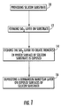
FIG. 7 is an SEM image of PIN diode that has been fabricated in accordance with the invention;
FIG. 8 is a cross-sectional FIB image of the PIN diode of FIG. 7;
FIG. 9 is a I-V curve for a P-I-N diode that is in accordance with one embodiment of the invention; and
FIG. 10 is a I-V curve continuous sweep test for a P-I-N diode that is in accordance with one embodiment of the invention.
DETAILED DESCRIPTION OF THE INVENTION
The present invention now will be described more fully hereinafter with reference to the accompanying drawings, in which some, but not all embodiments of the inventions are shown. Indeed, these inventions may be embodied in many different forms and should not be construed as limited to the embodiments set forth herein; rather, these embodiments are provided so that this disclosure will satisfy applicable legal requirements. Like numbers refer to like elements throughout.
With reference to FIG. 1 a process of selectively depositing a germanium nanofilm layer on a silicon substrate is schematically illustrated. In a first step, a silicon substrate is provided. Block 10. A layer of silicon dioxide (SiO2) is then formed on the substrate. Block 12. The SiO2 layer is then etched using photolithography techniques to produce one or more openings in the SiO2 layer to expose select regions of the surface of the silicon substrate. In one embodiment, the openings define openings that extend through the thickness of the SiO2 layer to thereby expose select regions of an underlying layer. Block 14. A germanium nanofilm layer is then epitaxially grown within the openings so that the germanium nanofilm layer is in direct physical contact with the silicon layer. Block 16. In this way, the germanium nanofilm layer is selectively deposited in the openings with little to none of the germanium being deposited on the SiO2 layer. For example, in one embodiment, the germanium nanofilm layer is limited to being present in the one or more openings formed in the SiO2 layer with no germanium being deposited on the surface of the SiO2 layer.
In some embodiments, the germanium nanofilm layer desirably has a thickness ranging from about 10 to 5,000 nanometers (nm), and more desirably from about 100 to 1,000 nm. In one embodiment, the germanium nanofilm layer is formed by depositing a plurality of tightly and closely spaced nanodots on the exposed silicon substrate surface. Ideally, the spacing of the germanium nanodots is such that the nanodots coalesce to have a continuous film-like structure. Typically, the initial deposition of the germanium nanodots is such that the spacing between adjacent dots is no more than 1 nm, and more typically no more than 10 nm. Generally, each nanodot can have a height or thickness of approximately 5 nm-50 nm and a diameter on the order of approximately 5 nm. It should be recognized that the dimensions of the nanodots can be adapted in accordance with the requirements of the particular application and device being fabricated. For example, wavelength of emission can be matched to a waveguide and/or detector for optical signal transmission.
Generally, the germanium nanodoats can be deposited at temperatures ranging from about 450° C. to 1000° C., and at pressures from about 10 to 760 Torr, with a pressure of about 20 Torr being somewhat preferred. In one embodiment, the deposition of the germanium nanodots is carried out a temperature from about 450 to 930° C. and at a pressure from about 10 to 60 torr.
It is believed that the coalescing of the germanium nanodots is due to high energy surfaces, especially surfaces which have been etched. As the nanodots initially grow, the nanodots tend to initiate at these high energy surfaces as oppose to low energy surfaces, such as unetched silicon. As the nanodots continue to grow, in close proximity to each other, the nanodots touch and fuse by overcoming the lattice mismatch between germanium and silicon. It is believed that the lattice mismatch between germanium and silicon is a significant factor in the initial growth of germanium as a nanodot.
As discussed in greater detail below, the germanium nanofilm layer, as well as a layer from which the SiO2 layer is formed, can be deposited utilizing a variety of different techniques including Metal Organic Vapor Phase epitaxy processes (MO-CVD), molecular beam epitaxial processes (MBE) chemical vapor deposition (CVD), physical vapor deposition (PVD) and other thin film deposition processes.
The openings in the SiO2 layer can be made using photolithography techniques, such as plasma dry etch or hydrofluoric acid wet etch. As will be appreciated by one of skill in the art, the number of openings, thickness of the openings, and the pattern of the openings can be selected based on the desired semiconductor device and its intended application. For example, the SiO2 layer can be etched to have a desired pattern so that the resulting germanium nanofilm layer also has a desired pattern. As a result, semiconductor devices can be fabricated having a germanium nanofilm layer with a desired pattern without the need to pattern and etch a germanium film layer.
In a further embodiment, the present invention can be used to prepare semiconductor devices in which an intrinsic layer, such as an intrinsic silicon layer or intrinsic germanium layer is disposed between the germanium nanofilm layer and the silicon substrate. For instance, prior to forming the SiO2 layer, an intrinsic silicon layer can be deposited on the surface of the silicon substrate. The intrinsic silicon layer can be deposited with epitaxy processes as discussed above. In a subsequent step, a portion of the intrinsic silicon layer can be oxidized to form the SiO2 layer. The SiO2 layer can then be patterned and etched to form one or more openings in which a surface of the intrinsic layer is exposed. The germanium nanofilm layer can then be epitaxially deposited onto the exposed surface of the intrinsic silicon layer. As discussed in greater detail below, this embodiment of the present invention can be used to fabricate P-I-N type or N-I-P type diodes, among other types of semiconductor devices.
For example, in one embodiment a semiconductor device can be fabricated in which the silicon substrate has a P-type conductivity, such as P, P+, P++, etc., and the germanium nanofilm layer has a N-type conductivity, such as N, N +, N ++, etc. Alternatively, the silicon substrate can have an N-type conductivity, such as, N, N +, N ++ etc., and the germanium nanofilm layer can have a P-type conductivity, such as P, P+, P++, etc. Exemplary N-type doping materials include phosphorus, arsenic, and antimony. Exemplary P-type doping materials include boron and aluminum. The silicon layer and the germanium nanofilm layer can be doped with N- or P-type material using methods known in the art.
With reference to FIG. 2 a process of preparing a semiconductor device in accordance with one embodiment of the present invention is schematically illustrated. In a first step, a silicon substrate of a first conductivity is provided. Block 20. Next, a layer of silicon is deposited onto the surface of the silicon substrate. Block 22. An outer portion of the silicon layer is then oxidized to form a SiO2 layer and an intrinsic silicon layer on the silicon substrate. Block 24. The intrinsic silicon layer is disposed between the silicon substrate and the outer SiO2 layer. The SiO2 layer is then etched using photolithography techniques to produce one or more openings in the SiO2 layer to expose select regions of the surface of the intrinsic silicon layer. Block 26. A germanium nanofilm layer of a second conductivity type is then epitaxially grown within the openings so that the germanium nanofilm layer is in direct physical contact with the intrinsic silicon layer. Block 28.
Generally, each layer of the semiconductor device (e.g., SiO2 layer, intrinsic silicon layer, germanium nanofilm layer, etc.) is disposed on a preceding layer so that the layers are positionally on or over another layer regardless of whether there are any intervening layers. For example, if one layer is positioned on another layer, this does not necessarily mean that the two layers are in physical contact with each other.
With reference to FIGS. 3-5, exemplary semiconductor devices that are in accordance with embodiments of the present invention are illustrated. In the illustrated embodiments, the semiconductor devices comprise diodes of the P-I-N type. It should be understood that an N-I-P device can also be fabricated and operate in accordance with the present invention. Selection of device type depends on the particular application in which the device is being used. Turning to FIG. 3, a semiconductor device 30 is illustrated in which the device includes a silicon substrate 32 of a first conductivity-type; an intrinsic layer 34, a silicon dioxide layer 36 having one or more openings 38 formed therein, and a germanium nanofilm layer 40 of a second conductivity type disposed in the openings and in direct physical contact with the surface 42 intrinsic layer.
In this embodiment, a silicon substrate 32 that has been doped with either a P- or N-type semiconductor material is provided. An intrinsic silicon layer 34 is then deposited on the silicon substrate 32 using MOCVD epitaxy. Generally, the thickness of the intrinsic silicon layer 34 can range from between about 20 to 400 nm. For example, the intrinsic silicon layer can have a thickness from about 20 to 100 nm. An outer portion of the intrinsic silicon layer 34 is oxidized to form SiO2 layer 36. The intrinsic silicon layer can be oxidized, for example, using a dry oxygen or wet oxygen environment under high temperature to grow the SiO2 layer. Typically, the oxidation of the intrinsic silicon layer is carried out at a temperature from about 800 to 1,200 C, and more typically from about 850 to 1,000 C. In the illustrated embodiment, the thickness of the SiO2 layer can be selected based on a desired and/or expected thickness of the germanium nanofilm layer 40. Typically, the thickness of the SiO2 layer is between about 10 to 100 nm, and more typically between about 50 and 100 nm.
After the SiO2 layer has been formed, a photolithography mask can be used to pattern and etch the SiO2 layer to form one or more openings in the SiO2 layer. The SiO2 layer is desirably etched to expose at least a portion of the surface of the intrinsic silicon layer. The germanium nanofilm layer 40 is then grown in the openings using a deposition process, such as MOCVD. As discussed above, the germanium nanofilm layer is created in the opening(s) by depositing a plurality of tightly packed nanodots that coalesce to create a continuous germanium nanofilm layer in each of the openings. The germanium nanofilm layer is desirably a different conductivity type than the silicon substrate.
In some embodiments, metal contact layers 44, 46 are formed on opposite sides of the semiconductor device 30. Suitable materials for the contact layers include gold, copper, and aluminum. The contact layers can be formed using deposition processes discussed above, such as PVD (physical vapor deposition). The thickness of the contact layers generally ranges between about 50 to 5,000 nm. Typically metal evaporation, such as e-beam or resistance heated, can also be used to form the contact layers.
FIG. 4 illustrates an embodiment of a semiconductor device 30 a in which an intrinsic germanium nanofilm layer 48 is deposited in direct physical contact with at least a portion of the surface 54 of the silicon substrate 32. The surface 54 of the silicon substrate 32 is exposed by etching one or more openings in the SiO2 layer 36 as discussed above. A second silicon layer 50 having a different conductivity than the silicon substrate is then deposited in the opening on at least a portion of the surface 56 of the intrinsic germanium nanofilm layer 48. For example, the silicon substrate 32 can have a conductivity of the P-type whereas the second silicon layer 50 has a conductivity of the N-type, and vice versa.
As shown in FIG. 4, the SiO2 layer 36 can be formed directly on the surface 54 of the silicon substrate, and can then be etched to expose a portion of the surface 54 of the silicon substrate. The intrinsic germanium nanofilm layer 48 is then deposited within the opening 38 in direct physical contact with the thus exposed surface 54 of the silicon substrate. Generally, the intrinsic germanium nanofilm layer has a thickness between about 5 to 50 nm, and more typically between about 10 to 30 nm, and the second silicon layer 50 has a thickness between about 10 to 100 nm, and more typically between about 25 to 75 nm. Typically, the thickness of the intrinsic germanium nanofilm layer 50 is between about 10 to 50% of the total depth of the opening. Contacts 44, 46 can then be formed on opposite sides of the semiconductor device 20 a as discussed above.
In one embodiment, the present invention provides a semiconductor device having an intrinsic silicon layer with a thickness that ranges from about 10 to 100 nm, and a germanium nanofilm layer having a thickness ranging from about 25 to 250 nm.
FIG. 5 illustrates a further embodiment of a semiconductor device 30 b in which an intrinsic germanium nanofilm layer 48 is deposited in direct physical contact with at least a portion of the surface 54 of silicon substrate 32. A second germanium nanofilm layer 40 having a different conductivity than the silicon substrate 32 is deposited in the opening on the intrinsic germanium nanofilm layer. For example, the silicon substrate 32 can have a conductivity of the P-type whereas the second germanium nanofilm layer 40 has a conductivity of the N-type, and vice versa.
As shown in FIG. 5, the SiO2 layer 36 can be formed directly on the surface 54 of the silicon substrate, and can then be etched to expose a portion of the surface of the silicon substrate. The intrinsic germanium nanofilm layer can then be deposited within the opening in direct physical contact with the thus exposed surface of the silicon substrate as discussed above in connection with FIG. 4. The second germanium nanofilm layer is then deposited in the opening 38 on the surface 56 of the intrinsic germanium nanofilm layer as discussed above. Contacts 44, 46 can then be formed on opposite sides of the semiconductor device 30 b. The thicknesses of each respective layer are generally in accordance with the embodiment discussed above in connection with FIG. 3.
As briefly noted above, embodiments of the present invention can be used to fabricate a wide variety of semiconductor devices including P-I-N diodes and N-I-P diodes, as well as advanced semiconductor devices such as CMOS and MOSFET devices.
EXAMPLE 1
A silicon substrate measuring 150 mm in diameter and having a major surface in the (100) plane was utilized. A 100 nm thermal silicon oxide layer was patterned and etched to expose select regions of the surface of the silicon substrate. A germanium nanofilm layer was then epitaxially grown in the openings on the exposed surfaces of the silicon substrate. An ASM Epsilon 2000 Epitaxy Reactor was used to chemically vapor deposit the germanium nanofilm layer within the openings. The initial deposition was carried out at a temperature of 650° C. for one minute. A germanium nanofilm layer was grown using 180 sccm Germane gas (1% in H2 carrier gas) at a reduced pressure of 20 torr. 20 SLM H2 was used as the carrier gas. This first deposition was followed by a second deposition for an additional minute with a reactor temperature of 925° C. FIG. 6 is an SEM image at 9,150 times magnification of the surface of the silicon substrate that shows the selective deposition of the germanium nanofilm layer in the etched openings. No germanium is detectable on the surface of the SiO2 layer.
The SiO2 was etched using a dry etch plasma utilizing a photolithography mask to define the openings. After etching, the photoresist was removed by ashing the photoresist. Prior to germanium growth, the wafer was dipped in dilute Hydrofluoric acid to remove native oxide growth (˜75 A of SiO2 is removed). A hydrogen terminated silicon surface was the starting point for germanium growth.
EXAMPLE 2
In this example, a PIN diode was formed having an intrinsic germanium nanofilm layer. A silicon substrate measuring 150 mm in diameter and having a major surface in the (100) plane was utilized. A 100 nm thermal silicon oxide layer was patterned and etched to expose select regions of the surface of the silicon substrate. An intrinsic germanium nanofilm layer was then epitaxially grown in the openings on the exposed surfaces of the silicon substrate. An ASM Epsilon 2000 Epitaxy Reactor was used to chemically vapor deposit the germanium nanofilm layer within the openings. The reactor temperature was at 650° C. The intrinsic germanium nanofilm layer was grown using 180 sccm Germane gas (1% in H2 carrier gas) for 1 minute deposition at a pressure of 20 torr. Next, an N-doped layer of germanium was deposited in the openings on the surface of the intrinsic germanium nanofilm layer. The deposition was performed for 2 minutes at a reactor temperature of 650° C. 55 ppm Arsine in hydrogen was used as the dopant gas. FIG. 7 is an SEM image at 15,100× magnification of the resulting PIN diode that shows selective deposition of the intrinsic germanium nanofilm layer and the N-doped germanium nanofilm layer within the etched openings. FIG. 7 depicts the Intrinsic and N-region selectively deposited in the oxide openings. The SEM shows a film in the middle of the openings with more coalesced nanodots on the edges of the oxide openings. FIG. 8 is a focused ion beam (FIB) cross-sectional image of the PIN diode that was taken with at 100,000×. FIG. 8 shows that the thickness of the germanium nanofilm was about 85 nm. No germanium can be seen on the surface of the SiO2 layer.
FIGS. 9 and 10 are IV curves of the PIN device fabricated on P+ Silicon. An intrinsic layer of germanium was first selectively deposited on the Silicon and a subsequent N+ doped germanium film was deposited on top of the i-Ge. FIG. 9 is a forward sweep from −5 volts to +20 volts on the PIN device. Turn on voltage was around 5 volts. At approximately 11 volts the current was above the tester's current limit.
Many modifications and other embodiments of the inventions set forth herein will come to mind to one skilled in the art to which these inventions pertain having the benefit of the teachings presented in the foregoing descriptions and the associated drawings. Therefore, it is to be understood that the inventions are not to be limited to the specific embodiments disclosed and that modifications and other embodiments are intended to be included within the scope of the appended claims. Although specific terms are employed herein, they are used in a germaniumneric and descriptive sense only and not for purposes of limitation.

Claims (11)

1. A semiconductor device comprising:
a silicon layer of a first conductivity-type;
an intrinsic layer comprising silicon disposed on said silicon layer;
an SiO2 layer having one or more openings formed therein; and
a germanium nanofilm layer of a second conductivity-type disposed in said openings and in direct physical contact with said intrinsic layer.
2. The semiconductor device of claim 1, wherein the germanium nanofilm layer has a thickness of between 100 to 1,000 nm.
3. The semiconductor device of claim 1, wherein the presence of the germanium nanoflim is substantially limited to being present in the one or more openings formed in the SiO2 layer.
4. The semiconductor device of claim 1, wherein the semiconductor device comprises a PIN or NIP diode.
5. A semiconductor device comprising:
a silicon substrate of a first conductivity-type;
an intrinsic silicon layer disposed on said substrate;
an SiO2 layer disposed on the intrinsic silicon layer and having one or more openings formed therein in which the surface of the intrinsic silicon layer is exposed; and
a germanium nanofilm layer of a second conductivity-type disposed in said openings and in direct physical contact with said exposed regions of the intrinsic silicon layer.
6. The semiconductor device of claim 5, wherein in the germanium nanofilm layer comprises a plurality of tightly spaced germanium nanodots.
7. The semiconductor device of claim 5, wherein intrinsic silicon layer has a thickness that ranges from about 10 to 100 nm, and the germanium nanofilm layer has a thickness ranging from about 25 to 250 nm.
8. The semiconductor device of claim 5, further comprising a metal layer disposed on a surface of the silicon substrate that is opposite the intrinsic silicon layer, and a second metal layer disposed at least partially on the surface of the germanium nanofilm layer.
9. A semiconductor device comprising:
a silicon substrate of a first conductivity-type;
an SiO2 layer disposed on the silicon substrate and having one or more openings formed therein so that a surface of silicon substrate is exposed, wherein said one or more openings have a first depth;
an intrinsic germanium nanofilm layer disposed in said openings and in direct physical contact with said exposed regions of the silicon substrate so that at least a portion of the germanium nanofilm layer is in direct physical contact with said silicon substrate; and
a silicon layer of a second conductivity type disposed in said one or more openings so that the intrinsic germanium nanofilm layer is disposed between the silicon substrate and the silicon layer.
10. The semiconductor device of claim 9, wherein the semiconductor device is a PIN diode.
11. The semiconductor device of claim 9, wherein the semiconductor device is a NIP diode.
US12/136,193 2008-06-10 2008-06-10 Semiconductor devices that include germanium nanofilm layer disposed within openings of silicon dioxide layer Active US7737534B2 (en)

Priority Applications (2)

Application Number Priority Date Filing Date Title
US12/136,193 US7737534B2 (en) 2008-06-10 2008-06-10 Semiconductor devices that include germanium nanofilm layer disposed within openings of silicon dioxide layer
EP09162210.0A EP2133534B1 (en) 2008-06-10 2009-06-08 Nucleate boiling cooling system and method

Applications Claiming Priority (1)

Application Number Priority Date Filing Date Title
US12/136,193 US7737534B2 (en) 2008-06-10 2008-06-10 Semiconductor devices that include germanium nanofilm layer disposed within openings of silicon dioxide layer

Publications (2)

Publication Number Publication Date
US20090302426A1 US20090302426A1 (en) 2009-12-10
US7737534B2 true US7737534B2 (en) 2010-06-15

Family

ID=40957881

Family Applications (1)

Application Number Title Priority Date Filing Date
US12/136,193 Active US7737534B2 (en) 2008-06-10 2008-06-10 Semiconductor devices that include germanium nanofilm layer disposed within openings of silicon dioxide layer

Country Status (2)

Country Link
US (1) US7737534B2 (en)
EP (1) EP2133534B1 (en)

Cited By (7)

* Cited by examiner, † Cited by third party
Publication number Priority date Publication date Assignee Title
US9864138B2 (en) 2015-01-05 2018-01-09 The Research Foundation For The State University Of New York Integrated photonics including germanium
US10698156B2 (en) 2017-04-27 2020-06-30 The Research Foundation For The State University Of New York Wafer scale bonded active photonics interposer
US10816724B2 (en) 2018-04-05 2020-10-27 The Research Foundation For The State University Of New York Fabricating photonics structure light signal transmission regions
US10877300B2 (en) 2018-04-04 2020-12-29 The Research Foundation For The State University Of New York Heterogeneous structure on an integrated photonics platform
US10976491B2 (en) 2016-11-23 2021-04-13 The Research Foundation For The State University Of New York Photonics interposer optoelectronics
US11029466B2 (en) 2018-11-21 2021-06-08 The Research Foundation For The State University Of New York Photonics structure with integrated laser
US11550099B2 (en) 2018-11-21 2023-01-10 The Research Foundation For The State University Of New York Photonics optoelectrical system

Families Citing this family (8)

* Cited by examiner, † Cited by third party
Publication number Priority date Publication date Assignee Title
US8290325B2 (en) * 2008-06-30 2012-10-16 Intel Corporation Waveguide photodetector device and manufacturing method thereof
US8384183B2 (en) * 2010-02-19 2013-02-26 Allegro Microsystems, Inc. Integrated hall effect element having a germanium hall plate
EP2682582B1 (en) * 2011-03-03 2016-12-21 Toyota Jidosha Kabushiki Kaisha Warmup acceleration device for internal combustion engine
JP5831165B2 (en) * 2011-11-21 2015-12-09 富士通株式会社 Semiconductor optical device
FR2997449B1 (en) * 2012-10-26 2019-05-17 Valeo Systemes Thermiques COOLING SYSTEM FOR MOTOR VEHICLE ENGINE
RU2621370C2 (en) * 2015-09-18 2017-06-02 федеральное государственное бюджетное образовательное учреждение высшего образования Кабардино-Балкарский государственный университет им. Х.М. Бербекова Method for semiconductor device manufacture
US11342469B2 (en) * 2018-07-09 2022-05-24 Macom Technology Solutions Holdings, Inc. Vertical etch heterolithic integrated circuit devices
US11613807B2 (en) * 2020-07-29 2023-03-28 The Curators Of The University Of Missouri Area selective nanoscale-thin layer deposition via precise functional group lithography

Citations (23)

* Cited by examiner, † Cited by third party
Publication number Priority date Publication date Assignee Title
US4092210A (en) 1975-08-18 1978-05-30 Siemens Aktiengesellschaft Process for the production of etched structures in a surface of a solid body by ionic etching
US4423127A (en) 1980-12-29 1983-12-27 Fujitsu Limited Method of manufacturing a semiconductor device
US4476481A (en) 1981-08-31 1984-10-09 Tokyo Shibaura Denki Kabushiki Kaisha Low-loss P-i-n diode
US4514748A (en) 1983-11-21 1985-04-30 At&T Bell Laboratories Germanium p-i-n photodetector on silicon substrate
US4600935A (en) 1984-11-14 1986-07-15 Rca Corporation Back-to-back diodes
US4604636A (en) 1983-05-11 1986-08-05 Chronar Corp. Microcrystalline semiconductor method and devices
US4885622A (en) 1984-03-23 1989-12-05 Oki Electric Industry Co., Ltd. Pin photodiode and method of fabrication of the same
US5077875A (en) 1990-01-31 1992-01-07 Raytheon Company Reactor vessel for the growth of heterojunction devices
US5293050A (en) 1993-03-25 1994-03-08 International Business Machines Corporation Semiconductor quantum dot light emitting/detecting devices
US5503959A (en) 1991-10-31 1996-04-02 Intel Corporation Lithographic technique for patterning a semiconductor device
US5562770A (en) 1994-11-22 1996-10-08 International Business Machines Corporation Semiconductor manufacturing process for low dislocation defects
US5693139A (en) 1984-07-26 1997-12-02 Research Development Corporation Of Japan Growth of doped semiconductor monolayers
US5963800A (en) 1995-06-16 1999-10-05 Interuniversitair Micro-Elektronica Centrum (Imec Vzw) CMOS integration process having vertical channel
US20040197945A1 (en) 2003-04-05 2004-10-07 Rohm And Haas Electronic Materials L.L.C. Germanium compounds
US7008813B1 (en) 2005-02-28 2006-03-07 Sharp Laboratories Of America, Inc.. Epitaxial growth of germanium photodetector for CMOS imagers
US7049181B2 (en) 2002-05-03 2006-05-23 M/A-Com Method of making heterojunction P-I-N diode
US20070001581A1 (en) 2005-06-29 2007-01-04 Stasiak James W Nanostructure based light emitting devices and associated methods
US7186611B2 (en) * 2005-02-28 2007-03-06 Sharp Laboratories Of America, Inc. High-density germanium-on-insulator photodiode array
US20070099315A1 (en) * 2005-10-27 2007-05-03 Sharp Laboratories Of America, Inc. Germanium photo detector having planar surface through germanium epitaxial overgrowth
US20070105256A1 (en) 2005-11-01 2007-05-10 Massachusetts Institute Of Technology Monolithically integrated light emitting devices
US7238595B2 (en) 2003-03-13 2007-07-03 Asm America, Inc. Epitaxial semiconductor deposition methods and structures
US7256416B2 (en) 2003-08-18 2007-08-14 Rohm Co., Ltd. Semiconductor light emitting device
US7259084B2 (en) 2003-07-28 2007-08-21 National Chiao-Tung University Growth of GaAs epitaxial layers on Si substrate by using a novel GeSi buffer layer

Family Cites Families (4)

* Cited by examiner, † Cited by third party
Publication number Priority date Publication date Assignee Title
US4768484A (en) 1987-07-13 1988-09-06 General Motors Corporation Actively pressurized engine cooling system
GB9524949D0 (en) * 1995-12-06 1996-02-07 Kodak Ltd Bubble detector
US6230669B1 (en) 1996-11-13 2001-05-15 Evans Cooling Systems, Inc. Hermetically-sealed engine cooling system and related method of cooling
US7069883B2 (en) * 2000-10-19 2006-07-04 Atkins Robert M Monitoring of closed circuit liquid cooling systems particularly in internal combustion engines

Patent Citations (25)

* Cited by examiner, † Cited by third party
Publication number Priority date Publication date Assignee Title
US4092210A (en) 1975-08-18 1978-05-30 Siemens Aktiengesellschaft Process for the production of etched structures in a surface of a solid body by ionic etching
US4423127A (en) 1980-12-29 1983-12-27 Fujitsu Limited Method of manufacturing a semiconductor device
US4476481A (en) 1981-08-31 1984-10-09 Tokyo Shibaura Denki Kabushiki Kaisha Low-loss P-i-n diode
US4604636A (en) 1983-05-11 1986-08-05 Chronar Corp. Microcrystalline semiconductor method and devices
US4514748A (en) 1983-11-21 1985-04-30 At&T Bell Laboratories Germanium p-i-n photodetector on silicon substrate
US4885622A (en) 1984-03-23 1989-12-05 Oki Electric Industry Co., Ltd. Pin photodiode and method of fabrication of the same
US5693139A (en) 1984-07-26 1997-12-02 Research Development Corporation Of Japan Growth of doped semiconductor monolayers
US4600935A (en) 1984-11-14 1986-07-15 Rca Corporation Back-to-back diodes
US5077875A (en) 1990-01-31 1992-01-07 Raytheon Company Reactor vessel for the growth of heterojunction devices
US5503959A (en) 1991-10-31 1996-04-02 Intel Corporation Lithographic technique for patterning a semiconductor device
US5293050A (en) 1993-03-25 1994-03-08 International Business Machines Corporation Semiconductor quantum dot light emitting/detecting devices
US5562770A (en) 1994-11-22 1996-10-08 International Business Machines Corporation Semiconductor manufacturing process for low dislocation defects
US5963800A (en) 1995-06-16 1999-10-05 Interuniversitair Micro-Elektronica Centrum (Imec Vzw) CMOS integration process having vertical channel
US7049181B2 (en) 2002-05-03 2006-05-23 M/A-Com Method of making heterojunction P-I-N diode
US7238595B2 (en) 2003-03-13 2007-07-03 Asm America, Inc. Epitaxial semiconductor deposition methods and structures
US20040197945A1 (en) 2003-04-05 2004-10-07 Rohm And Haas Electronic Materials L.L.C. Germanium compounds
US7141488B2 (en) 2003-04-05 2006-11-28 Rohm And Haas Electronic Materials Llc Method of depositing germanium-containing films
US20070077733A1 (en) 2003-04-05 2007-04-05 Rohm And Haas Electronic Materials Llc Germanium compound delivery device
US7259084B2 (en) 2003-07-28 2007-08-21 National Chiao-Tung University Growth of GaAs epitaxial layers on Si substrate by using a novel GeSi buffer layer
US7256416B2 (en) 2003-08-18 2007-08-14 Rohm Co., Ltd. Semiconductor light emitting device
US7008813B1 (en) 2005-02-28 2006-03-07 Sharp Laboratories Of America, Inc.. Epitaxial growth of germanium photodetector for CMOS imagers
US7186611B2 (en) * 2005-02-28 2007-03-06 Sharp Laboratories Of America, Inc. High-density germanium-on-insulator photodiode array
US20070001581A1 (en) 2005-06-29 2007-01-04 Stasiak James W Nanostructure based light emitting devices and associated methods
US20070099315A1 (en) * 2005-10-27 2007-05-03 Sharp Laboratories Of America, Inc. Germanium photo detector having planar surface through germanium epitaxial overgrowth
US20070105256A1 (en) 2005-11-01 2007-05-10 Massachusetts Institute Of Technology Monolithically integrated light emitting devices

Cited By (16)

* Cited by examiner, † Cited by third party
Publication number Priority date Publication date Assignee Title
US10295745B2 (en) 2015-01-05 2019-05-21 The Research Foundation For The State University Of New York Integrated photonics including germanium
US10571631B2 (en) 2015-01-05 2020-02-25 The Research Foundation For The State University Of New York Integrated photonics including waveguiding material
US10830952B2 (en) 2015-01-05 2020-11-10 The Research Foundation For The State University Of New York Integrated photonics including germanium
US11703643B2 (en) 2015-01-05 2023-07-18 The Research Foundation For The State University Of New York Integrated photonics including waveguiding material
US9864138B2 (en) 2015-01-05 2018-01-09 The Research Foundation For The State University Of New York Integrated photonics including germanium
US10976491B2 (en) 2016-11-23 2021-04-13 The Research Foundation For The State University Of New York Photonics interposer optoelectronics
US11435523B2 (en) 2017-04-27 2022-09-06 The Research Foundation For The State University Of New York Wafer scale bonded active photonics interposer
US10698156B2 (en) 2017-04-27 2020-06-30 The Research Foundation For The State University Of New York Wafer scale bonded active photonics interposer
US11841531B2 (en) 2017-04-27 2023-12-12 The Research Foundation For The State University Of New York Wafer scale bonded active photonics interposer
US10877300B2 (en) 2018-04-04 2020-12-29 The Research Foundation For The State University Of New York Heterogeneous structure on an integrated photonics platform
US11550173B2 (en) 2018-04-04 2023-01-10 The Research Foundation For The State University Of New York Heterogeneous structure on an integrated photonics platform
US11378739B2 (en) 2018-04-05 2022-07-05 The Research Foundation For The State University Of New York Fabricating photonics structure light signal transmission regions
US10816724B2 (en) 2018-04-05 2020-10-27 The Research Foundation For The State University Of New York Fabricating photonics structure light signal transmission regions
US11635568B2 (en) 2018-04-05 2023-04-25 The Research Foundation For The State University Of New York Photonics light signal transmission
US11029466B2 (en) 2018-11-21 2021-06-08 The Research Foundation For The State University Of New York Photonics structure with integrated laser
US11550099B2 (en) 2018-11-21 2023-01-10 The Research Foundation For The State University Of New York Photonics optoelectrical system

Also Published As

Publication number Publication date
EP2133534A1 (en) 2009-12-16
EP2133534B1 (en) 2013-07-31
US20090302426A1 (en) 2009-12-10

Similar Documents

Publication Publication Date Title
US7737534B2 (en) Semiconductor devices that include germanium nanofilm layer disposed within openings of silicon dioxide layer
US11393940B2 (en) Photodetector and method for forming the same
US8198706B2 (en) Multi-level nanowire structure and method of making the same
US9184265B2 (en) Methods and apparatus for bipolar junction transistors and resistors
US8558282B1 (en) Germanium lateral bipolar junction transistor
KR101000941B1 (en) Germanium photodetector and method of forming the same
CN102171790A (en) Semiconductor substrate, electronic device and method for manufacturing semiconductor substrate
KR101142545B1 (en) Solar cell and manufacturing method of the same
KR20180053640A (en) Nanowires or nano-pyramids grown on a graphite substrate
JP2010520619A (en) Method for forming nanostructures on metal silicide crystallites, and structures and devices obtained by this method
CN101989630A (en) Mesa photodiode and method for manufacturing the same
CN111129228B (en) Method for manufacturing photoelectric detector
US20170077226A1 (en) Method of forming nanostructure, method of manufacturing semiconductor device using the same, and semiconductor device including nanostructure
KR20210046641A (en) 3-dimensional photodetector device and method of manufacturing thereof
CN111509078A (en) Silicon-based photoelectric detector and manufacturing method thereof
JP4765211B2 (en) Pin type light receiving element
KR101106913B1 (en) Metal-base nanowire transistor
Kohen et al. Enhanced photovoltaic performance of vapor–liquid–solid grown silicon nanowire array with radial heterojunction
US20020110946A1 (en) Metamorphic long wavelength high-speed photodiode
US20060260676A1 (en) Photodetector
US20140202378A1 (en) METHOD FOR PRODUCING AN ORGANISED NETWORK OF SEMICONDUCTOR NANOWIRES, IN PARTICULAR MADE OF ZnO
JPH04102334A (en) Manufacture of semiconductor device
US20020197836A1 (en) Method of forming variable oxide thicknesses across semiconductor chips
KR20090056934A (en) Photodetector and method for manufacturing photodetector
CN114256147B (en) Method for preparing semiconductor structure

Legal Events

Date Code Title Description
AS Assignment

Owner name: NORTHROP GRUMMAN SYSTEMS CORPORATION, CALIFORNIA

Free format text: ASSIGNMENT OF ASSIGNORS INTEREST;ASSIGNORS:MCLAUGHLIN, SEAN R.;SINGH, NARSHINGH BAHADUR;WAGNER, BRIAN;AND OTHERS;REEL/FRAME:021071/0209;SIGNING DATES FROM 20080530 TO 20080602

Owner name: NORTHROP GRUMMAN SYSTEMS CORPORATION,CALIFORNIA

Free format text: ASSIGNMENT OF ASSIGNORS INTEREST;ASSIGNORS:MCLAUGHLIN, SEAN R.;SINGH, NARSHINGH BAHADUR;WAGNER, BRIAN;AND OTHERS;SIGNING DATES FROM 20080530 TO 20080602;REEL/FRAME:021071/0209

FEPP Fee payment procedure

Free format text: PAYOR NUMBER ASSIGNED (ORIGINAL EVENT CODE: ASPN); ENTITY STATUS OF PATENT OWNER: LARGE ENTITY

STCF Information on status: patent grant

Free format text: PATENTED CASE

CC Certificate of correction
FPAY Fee payment

Year of fee payment: 4

MAFP Maintenance fee payment

Free format text: PAYMENT OF MAINTENANCE FEE, 8TH YEAR, LARGE ENTITY (ORIGINAL EVENT CODE: M1552)

Year of fee payment: 8

MAFP Maintenance fee payment

Free format text: PAYMENT OF MAINTENANCE FEE, 12TH YEAR, LARGE ENTITY (ORIGINAL EVENT CODE: M1553); ENTITY STATUS OF PATENT OWNER: LARGE ENTITY

Year of fee payment: 12