US7720133B2 - Wireless communication apparatus, wireless communication method, propagation measurement apparatus and propagation measurement method - Google Patents
Wireless communication apparatus, wireless communication method, propagation measurement apparatus and propagation measurement method Download PDFInfo
- Publication number
- US7720133B2 US7720133B2 US11/210,864 US21086405A US7720133B2 US 7720133 B2 US7720133 B2 US 7720133B2 US 21086405 A US21086405 A US 21086405A US 7720133 B2 US7720133 B2 US 7720133B2
- Authority
- US
- United States
- Prior art keywords
- section
- spread
- code
- propagation measurement
- despread
- Prior art date
- Legal status (The legal status is an assumption and is not a legal conclusion. Google has not performed a legal analysis and makes no representation as to the accuracy of the status listed.)
- Expired - Fee Related, expires
Links
Images


Classifications
-
- H—ELECTRICITY
- H04—ELECTRIC COMMUNICATION TECHNIQUE
- H04B—TRANSMISSION
- H04B1/00—Details of transmission systems, not covered by a single one of groups H04B3/00 - H04B13/00; Details of transmission systems not characterised by the medium used for transmission
- H04B1/69—Spread spectrum techniques
- H04B1/707—Spread spectrum techniques using direct sequence modulation
- H04B1/7073—Synchronisation aspects
- H04B1/7075—Synchronisation aspects with code phase acquisition
- H04B1/708—Parallel implementation
-
- H—ELECTRICITY
- H04—ELECTRIC COMMUNICATION TECHNIQUE
- H04B—TRANSMISSION
- H04B1/00—Details of transmission systems, not covered by a single one of groups H04B3/00 - H04B13/00; Details of transmission systems not characterised by the medium used for transmission
- H04B1/69—Spread spectrum techniques
- H04B1/692—Hybrid techniques using combinations of two or more spread spectrum techniques
-
- H—ELECTRICITY
- H04—ELECTRIC COMMUNICATION TECHNIQUE
- H04B—TRANSMISSION
- H04B1/00—Details of transmission systems, not covered by a single one of groups H04B3/00 - H04B13/00; Details of transmission systems not characterised by the medium used for transmission
- H04B1/69—Spread spectrum techniques
- H04B1/7163—Spread spectrum techniques using impulse radio
- H04B1/71637—Receiver aspects
-
- H—ELECTRICITY
- H04—ELECTRIC COMMUNICATION TECHNIQUE
- H04B—TRANSMISSION
- H04B1/00—Details of transmission systems, not covered by a single one of groups H04B3/00 - H04B13/00; Details of transmission systems not characterised by the medium used for transmission
- H04B1/69—Spread spectrum techniques
- H04B1/7163—Spread spectrum techniques using impulse radio
- H04B1/717—Pulse-related aspects
- H04B1/7172—Pulse shape
-
- H—ELECTRICITY
- H04—ELECTRIC COMMUNICATION TECHNIQUE
- H04B—TRANSMISSION
- H04B1/00—Details of transmission systems, not covered by a single one of groups H04B3/00 - H04B13/00; Details of transmission systems not characterised by the medium used for transmission
- H04B1/69—Spread spectrum techniques
- H04B1/7163—Spread spectrum techniques using impulse radio
- H04B1/719—Interference-related aspects
-
- H—ELECTRICITY
- H04—ELECTRIC COMMUNICATION TECHNIQUE
- H04B—TRANSMISSION
- H04B2201/00—Indexing scheme relating to details of transmission systems not covered by a single group of H04B3/00 - H04B13/00
- H04B2201/69—Orthogonal indexing scheme relating to spread spectrum techniques in general
- H04B2201/707—Orthogonal indexing scheme relating to spread spectrum techniques in general relating to direct sequence modulation
- H04B2201/70707—Efficiency-related aspects
Definitions
- the present invention contains subject matter related to Japanese Patent Application JP 2004-266211 filed in the Japanese Patent Office on 14 Sep., 2004, the entire contents of which being incorporated herein by reference.
- the present invention relates to a wireless communication apparatus, a wireless communication method, a propagation measurement apparatus and a propagation measurement method for receiving a spectrum-spread transmission signal.
- the present invention concerns a wireless communication apparatus, a wireless communication method, a propagation measurement apparatus and a propagation measurement method for performing propagation measurement using a preamble section of the spectrum-spread transmission signal.
- the present invention relates to a wireless communication apparatus, a wireless communication method, a propagation measurement apparatus and a propagation measurement method for performing propagation measurement by despread of each spread code in the baseband section having a clock frequency not more than a chip rate in an RF section.
- the present invention concerns a wireless communication apparatus, a wireless communication method, a propagation measurement apparatus and a propagation measurement method for performing propagation measurement using a plurality of despreaders that despread each chip of a short code, in consideration of a trade-off between speed enhancement and circuit scale and power consumption.
- Canonical standards concerning wireless networks can include IEEE (The Institute of Electrical and Electronics Engineers) 802.11 (e.g., see non-patent document 1), HiperLAN ⁇ 2 (e.g., see non-patent document 2 or 3), IEEE802.15.3, and Bluetooth communication, for example.
- the IEEE802.11 has enhanced standards such as IEEE802.11a, IEEE802.11b, etc. depending on differences of wireless communication systems and frequency bands.
- ultra-wideband (UWB) communication for carrying out wireless communication that uses a very wide frequency band such as 3 GHz-10 GHz is attracting attention as a short-distance, ultra-high-speed wireless communication system, and is expected to be put to practical use (e.g., see non-patent document 4).
- UWB ultra-wideband
- a data transmission system having a packet structure including a preamble is being developed as an access control system of ultra-wideband (UWB) communication, in IEEE802.15.3 and the like.
- the UWB communication has high time resolution by employing very narrow pulses, and this property enables “Ranging” for radar and positioning.
- recent UWB communications can include high-speed data transmission exceeding 100 Mbps (e.g., see patent document 1) along with the original ranging function (e.g., see patent document 1).
- WPAN Wireless Personal Access Network
- UWB Wired Personal Access Network
- CE Consumer Electronics
- the SS systems include the DS (Direct Spread) system.
- the transmission side multiplies an information signal by a random code sequence called a PN (Pseudo Noise) code to spread an occupied band for transmission.
- the reception side multiplies the received spread information signal by the PN code to despread the information signal for reproduction.
- the UWB transmission system includes two types: DS-UWB and impulse-UWB.
- the DS-UWB system maximizes spread speeds of DS information signals.
- the impulse-UWB system employs an impulse signal sequence having a very short period of approximately several hundreds of picoseconds.
- the DS-UWB system can control spectra using PN code speeds, but needs to operate logic circuits with a high speed of the order of GHz, so that undesirably the power consumption easily increases.
- the impulse-UWB system can be configured in combination with a pulse generator and a low-speed logic circuit, so that there is an advantage of reducing the current consumption.
- Both systems can achieve high-speed data transmission by spreading signals to an ultra wide frequency band such as 3 GHz to 10 GHz for transmission and reception.
- the occupied bandwidth is of the order of GHz, and the occupied bandwidth divided by the center frequency (e.g., 1 GHz-10 GHz) is approximately 1.
- the occupied bandwidth is ultra wideband compared to bandwidths normally used in wireless LANs based on the W-CDMA or cdma2000 system, and the SS (Spread Spectrum) or OFDM (Orthogonal Frequency Division Multiplexing) system.
- the Gaussian monocycle pulse follows the equation below. In the equation, constants such as 3.16 and 3.3 are found to provide a spectrum equivalent to the rectangular wave monocycle pulse.
- FIG. 23 shows time waveforms.
- FIG. 24 shows a comparison between frequency characteristics of power spectrum densities for these monocycle pulses.
- a pulse of 100 MHz will yield the power density 80 dB higher than this value.
- the Gaussian monocycle pulse is almost the same as the rectangular wave monocycle pulse in the transmission band.
- the Gaussian monocycle pulse generates a higher peak voltage than the rectangular wave monocycle pulse, requires the linearity, and makes processing difficult including power amplification.
- FIG. 25 shows the frequency characteristics of power spectrum densities in FIG. 24 in terms of antilogarithms instead of decibels. Though there is no special need for using antilogarithms, the linear representation of energy provides many intuitive benefits.
- the spectrum has the following two requirements.
- the FCC specifications for spectrum masks disable radiation of 3 GHz or less.
- the band ranging from 4.9 GHz to 5.3 GHz contains a 5-GHz wireless LAN that should be avoided.
- FIG. 26 shows a configuration example (conventional example) of a receiver in the UWB communication system.
- the configuration of the receiver in FIG. 26 is similar to that of a DS-SS (direct sequence spread spectrum) receiver.
- the example in FIG. 26 assumes that the VCO oscillates at the same frequency as the pulse frequency.
- the receiver follows the VCO timing and generates a pulse train having data all set to zeros. Using this, the receiver generates three waveforms each deviated for half of pulse width T p , i.e., T p /2, and multiplies them by a received signal.
- the intentionally deviated VCO frequency is returned to the correct frequency.
- a tracking operation takes place in order to maintain this timing.
- the received signal is multiplied by the waveforms deviated for ⁇ T p /2 against the center (puncture) to find energies. Differences are used to detect positive and negative values corresponding to positive and negative pulse position errors. These values are supplied to loop filters and are used as control voltages for the pulse position tracking.
- the receiver configured as shown in FIG. 26 needs to divide a signal path into three and use three multiplication-oriented circuits, thus complicating the circuitry.
- the receiver needs to change frequencies for search and tracking operations.
- the time needed for this changeover prolongs the time for synchronization establishment.
- Pulse positions need to be correctly detected under a noise environment. For this purpose, it is necessary to detect that the energy increases more than once. A frequency is intentionally deviated by a slight amount. After the energy increases more than once, resulting values are averaged. Thereafter, pulse positions needed to be detected. Consequently, the time to establish the synchronization becomes lengthy.
- Analog circuits are used to configure systems for frequency deviation and tracking. However, analog circuits are often complex and are subject to variance, making it difficult to ensure stable operations.
- Energy values are used for the pulse position detection and tracking, thus degrading the S/N ratio and characteristics.
- Patent document 1 PCT Japanese Translation Patent Publication No. 2002-517001
- Non-patent document 1 International Standard ISO/IEC 8802-11:1999 (E) ANSI/IEEE Std 802.11, 1999 Edition, Part11: Wireless LAN Medium Access Control (MAC) and Physical Layer (PHY) Specifications
- Non-patent document 2 ETSI Standard ETSI TS 101-761-1V1.3.1 Broadband Radio Access Networks (BRAN); HIPERLAN Type 2; Data Link Control (DLC) Layer; Part1: Basic Data Transport Functions
- DS-SS direct sequence spread spectrum
- a wireless communication apparatus for receiving a code-spread transmission signal.
- the wireless communication apparatus includes an RF section, and a baseband section, wherein in the baseband section, despreaders of an integral submultiple, which is 1/n 1 , of the number of chips of a spread code are arranged in parallel, and there is provided a propagation measurement section that measures a propagation channel by using the plurality of despreaders a plurality of times in a time-division manner and performing despread of each period corresponding to a chip rate of the spread code.
- Ultra-wideband communication for carrying out wireless communication that uses a very wide frequency band such as 3 GHz-10 GHz is attracting attention as a short-range, ultra-high-speed wireless communication system, and is expected to be put to practical use. Further, there is also developed an ultra-wideband communication system combined with the DS-SS (direct sequence spread spectrum) for improving resistance to interfering waves.
- DS-SS direct sequence spread spectrum
- a receiver of a regular spread-spectrum (SS) system can operate the baseband at the same clock frequency as the chip rate.
- the use of the same clock frequency as the chip rate causes excessive power consumption. Therefore, in the wireless communication apparatus according to the embodiment of the present invention, the integral submultiple of the chip rate is employed as the clock frequency to the baseband section.
- a receiver of a regular spread-spectrum (SS) system can operate the baseband at the same clock frequency as the chip rate and perform propagation measurement by sliding correlation.
- the integral submultiple of the chip rate is employed as the clock frequency to the baseband section.
- the propagation measurement section despreads each short code to perform propagation measurement.
- the present invention in consideration of a trade-off between speed enhancement and circuit scale and power consumption, arrange in parallel a smaller number of despreaders than the number of chips of the spread code and use the despreaders several times in a time-division manner to perform despread computations on all chips.
- the propagation measurement section includes a delay line circuit that buffers parallel reception signals from the RF section and converts into serial data in chronological order, a plurality of despread circuits and accumulation circuits that are separated into a number of groups, a selector circuit that selects outputs of each group of despreaders and accumulators, a moving-average circuit that performs moving-average computations on propagation measurement results of the despread circuits and accumulation circuits, a memory circuit that stores values before and after a computation by the moving-average circuit, an energy calculation circuit that calculates an energy level of a reception signal, and a path detection circuit that sorts an energy value of each receiving position and outputs the energy value along with position information thereof.
- the propagation measurement section adopts as a propagation measurement value, a value obtained by despreading reception signal sampled at chip timing of A/D conversion in the RF section using a short code for propagation measurement.
- the configuration of the propagation measurement section enables high-speed propagation estimation, which enables high-speed detection of a symbol/pulse position.
- high-speed detection of a symbol/pulse enables operations such as CSMA (Carrier Sense Multiple Access) equivalent to a carrier sense, so that it becomes possible use random access systems such as CSMA. Further, it becomes possible to easily obtain parameters needed to RAKE reception using propagation estimation results.
- CSMA Carrier Sense Multiple Access
- the propagation measurement section may further include a rounding circuit that rounds selected output values of the despreaders and accumulators. In this case, the appropriate setting of computation accuracy leads to higher-speed circuit processing.
- the wireless communication apparatus may further include a reception control section that can control sampling timing of A/D conversion in the RF section. For example, after the completion of propagation measurement at in-chip phase 0/4, the sampling phase is shifted by 180 degrees, thereby enabling measurement at in-chip phase 2/4 as well. Thus, time resolution of a measurement period can be enhanced.
- the wireless communication apparatus may further includes a preamble end detection section that detects an end of a preamble signal, and a RAKE combining section that RAKE-combines energy of a multipath signal and demodulates a signal.
- the despread process separates an intended signal from the received signal composed of a plurality of delay waves superposed by a multipath propagation channel. Dispersed signal powers are unified. Since the direct sequence spread spectrum provides an effect of disassembling the time by dint of the despread, this effect is used to combine signals along separated paths by aligning the time and the phase.
- the reception signal is generally provided with a preamble section before a data signal to be received, the preamble section is provided with a periodic training section by a plurality of spread short codes having good autocorrelation properties. Further, the propagation measurement section and the preamble end detection section perform propagation measurement and preamble end detection with respective short codes. In this case, an information signal can be demodulated based on a high-speed propagation measurement result. Further, an end position of the preamble section, that is, a start position of data can be found accurately, thus improving reception performance.
- the preamble section is further provided with a symbol period spread by using any of the plurality of short codes in order to stabilize AGC. In this case, a reception signal level becomes constant during propagation measurement, thus improving reception performance.
- despread computations that each of the despread circuits performs per clock may be equal to the parallel number of input signals.
- parallel input signals to each of the despread circuits may be captured at given intervals from a plurality of taps in the delay line circuit.
- despread timing is given in such a manner that a control period becomes a relation of A ⁇ B clocks. In this case, circuit use efficiency increases, so that it becomes possible to reduce circuit scale.
- the propagation measurement section determines that a location where the largest energy is found out of propagation measurement values is a symbol/pulse position and performs a despread computation by a short code for preamble end detection at the pulse position to detect a preamble end position.
- the propagation measurement section removes an effect of a symbol pattern of a training section from a measured value by correlating a plurality of paths detected by the path detection circuit with symbol patterns respectively and further performs interpolation, thereby determining a final propagation measurement value. With this, resolution of propagation measurement can be enhanced, thus improving reception performance.
- the embodiment of the present invention it is possible to provide a method of high-speed propagation measurement in an ultra-wideband communication system combined with the DS-SS (direct sequence spread spectrum) for improving resistance to interfering waves.
- DS-SS direct sequence spread spectrum
- a wireless communication apparatus it is possible to provide a wireless communication apparatus, a wireless communication method, a propagation measurement apparatus and a propagation measurement method excellent at being able to perform propagation measurement by despread of each spread code in the baseband section having a clock frequency of an integral submultiple of a chip rate in the RF section.
- a wireless communication apparatus it is possible to provide a wireless communication apparatus, a wireless communication method, a propagation measurement apparatus and a propagation measurement method excellent at being able to perform propagation measurement using a plurality of despreaders that despread each chip of a short code, in consideration of a trade-off between speed enhancement and circuit scale and power consumption.
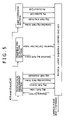
- FIG. 1 is an illustration schematically showing the configuration of an RF section in a wireless communication apparatus according to an embodiment of the present invention.
- FIG. 2 is an illustration showing signal wave images.
- FIG. 3 is an illustration schematically showing the configuration of a baseband section in a wireless communication apparatus according to an embodiment of the present invention.
- FIG. 4 is an illustration showing a configuration example of a signal format and a preamble pattern.
- FIG. 5 is an illustration showing a more detailed configuration of reception circuitry shown in FIG. 3 .
- FIG. 6 is an illustration exemplifying an image in which a propagation measurement section measures energy values for a 128-ns period at points 0/4 and 2/4 of in-chip phases.
- FIG. 7 shows an image in which a complex amplitude value having a ⁇ 2/4 in-chip phase difference from the position (Index) of a detected path is obtained from a propagation measurement section.
- FIG. 8 shows an image in which interpolation is performed using complex amplitude values of paths detected by a propagation estimation section and complex amplitude values at positions shifted by ⁇ 2/4 phase from the detected positions.
- FIG. 9 shows an image in which the amplitude values at points 1/4 and 3/4 of in-chip phases are interpolated over a 128-ns period based on the measurement values at points 0/4 and 2/4 of in-chip phases shown in FIG. 6 .
- FIG. 10 shows an image in which each of the 128 despreaders is shifted by 1 chip and 128 despread computations at respective points are processed concurrently.
- FIG. 12 is an illustration showing an operation sequence in which a physical layer sequence control section controls propagation measurement of a propagation measurement section.
- FIG. 13 is an illustration for explaining a measurement sequence obtaining the moving average of measurement results.
- FIG. 14 is an illustration for explaining a propagation measurement sequence.
- FIG. 15 is an illustration showing the circuit configuration of a propagation measurement section.
- FIG. 16 is an illustration showing the internal configuration of a delay line circuit.
- FIG. 17 is an illustration showing the internal configuration of a despreader and an accumulator.
- FIG. 18 shows an image of the control sequence of a selector circuit.
- FIG. 19 shows an image of the configuration of a moving-average circuit.
- FIG. 20 is an illustration showing the configuration of an equivalent circuit of the moving-average circuit shown in FIG. 19 .
- FIG. 21 is an illustration showing a configuration example of a memory map for storing propagation measurement data.
- FIG. 22 is an illustration showing a configuration example of a memory map for storing moving average data.
- FIG. 23 is an illustration showing a time waveform of a Gaussian monocycle pulse.
- FIG. 24 is an illustration showing frequency characteristics of power spectrum densities for a Gaussian and a rectangular monocycle pulses.
- FIG. 25 is an illustration showing frequency characteristics of power spectrum densities for a Gaussian and a rectangular monocycle pulses.
- FIG. 26 is an illustration showing a configuration example (conventional example) of a receiver in an ultra-wideband communication system.
- a UWB-based PAN Personal Area Network
- PAN Personal Area Network
- the use of the spectrum spread can set the C/I needed for enabling normal communication to a level lower than 0 dB. That is to say, if a user detects another user's signal at the same level as that of his or her own, the former is still capable of communication. This is especially easily available to the UWB because it occupies a much wider bandwidth than the required bit rate.
- the UWB's bandwidth depends on a pulse width independently of a pulse rate. While a wide bandwidth due to a narrow pulse width signifies a kind of spectrum spread, this is not discussed here for the following reason.
- the resistance to interfering waves takes effect if pulse positions differ occasionally.
- the resistance to interfering waves is not expected if pulse positions match by chance. In other words, it is a matter of chance. Therefore, it is preferable to perform the effective spectrum spread based on direct spread in addition to the spread based on a small pulse width.
- FIG. 1 schematically shows the configuration of an RF section in a wireless communication apparatus according to an embodiment of the present invention.
- the RF section shown in FIG. 1 is a transmitting/receiving apparatus of a typical ⁇ /2 shift BPSK (Binary Phase Shift Keying) system.
- the RF section can switch between 4 phases of a 1-GHz sampling frequency in accordance with a control signal from a baseband side after A/D conversion.
- a transmission signal sent from a baseband section is converted from parallel to serial form, and then divided into odd timing and even timing alternately by 500-MHz timing, for pulse shaping.
- the divided signals are BPSK-modulated by a carrier of 4 GHz in a quadrature relationship, then added, amplified by a power amplifier, and transmitted from an antenna through an RF filter.
- FIG. 2 shows signal wave images.
- a wireless signal received by the antenna goes through the RF filter and a low-noise amplifier.
- the amplified signal by frequency synthesis of the 4-GHz center frequency signal and the frequency signal having a 90-degree phase difference, for quadrature detection, is separated into I-axis and Q-axis signals and is subject to AGC based on RSSI (Received Signal Strength Indication). Further, the signals are sampled at 1-GHz as digital signals by an A/D converter. Furthermore, the sampled I/Q signals are converted from serial to parallel form, and then digitally processed by the baseband section.
- a 4-GHz local frequency generated by a local oscillator is a carrier frequency at the RF section.
- the carrier frequency is divided by four to provide the A/D converter with a sample rate, that is, a 1-GHz chip rate.
- the 1-GHz chip rate is further divided by eight to give a 125-MHz clock frequency to the baseband section (described later).
- the clock frequency to the baseband section is an integral submultiple of the chip rate and is selected from operating speeds that are practicable in the process.
- a receiver of a regular spread-spectrum (SS) system can operate the baseband at the same clock frequency as the chip rate.
- SS spread-spectrum
- the use of the same clock frequency as the chip rate causes excessive power consumption; therefore, the integral submultiple of the chip rate is employed.
- the oscillator switches chip timing; that is, an in-chip phase from 0/4 to 2/4 in response to a phase shift command (PhaseShift) from the baseband section.
- PhaseShift phase shift command
- FIG. 3 schematically shows the configuration of the baseband section in the wireless communication apparatus according to the embodiment of the present invention.
- Transmission circuitry in the baseband section shown in FIG. 3 includes a spread modulation section (Direct Spreader) that spreads an information signal.
- Reception circuitry in the baseband section includes a propagation measurement section (Channel Measure) that measures a delay profile of a propagation channel, a preamble end detection section (PreambleEndDetect) that detects the end of a preamble signal, and a RAKE combining section that RAKE-combines energy of a multipath signal and demodulates the signal.
- Each function section in the transmission/reception circuitry is subject to centralized control by a physical layer sequence control section (PhySequeneControl).
- Physical layer sequence control section Physical layer sequence control section
- the spread modulation section In the transmission circuitry of the baseband section, the spread modulation section directly spreads a transmission signal sent from a MAC layer control section corresponding to an upper layer of a communication protocol, and sends the spread signal to the transmission circuitry in the RF section. A description will be given later as to signal processing in the reception circuitry of the baseband section.
- FIG. 4 schematically shows an example of the format structure of a signal used for wireless transmission.
- a transmission signal is composed of a preamble (Preamble) section for performing processing for signal detection and synchronization, a PHY header section in which control information for a PHY layer is described, and a payload (Payload) section.
- the payload section can be further separated into a MAC header section and a MAC payload section, which are not directly related to the gist of the invention; therefore, a description thereof is omitted here.
- the preamble section is composed of short code patterns (Spread Sequence) consisting of 128 chips each.
- Spread Sequence Short Code Pattern
- Pattern B is repeated a plurality number of times at the head of the preamble section, which is used as an area for stabilizing AGC gain. In the example shown in FIG. 4 , pattern B is repeated three times for the AGC, and the relevant area needs to be ensured for just a period that allows the AGC to be stable.
- a training pattern for propagation measurement consisting of 10 symbols of pattern A is repeated five times to be arranged.
- the gist of the invention is not limited to the format structure shown in FIG. 4 , and it is possible to change a parameter value constituting each pattern as necessary.
- FIG. 5 shows a more detailed configuration of the reception circuitry shown in FIG. 3 .
- the reception circuitry in the baseband section includes the propagation measurement section (Channel Measure) that measures a delay profile of a propagation channel, the preamble end detection section (PreambleEndDetect) that detects the end of a preamble signal, and the RAKE combining section that RAKE-combines energy of a multipath signal and demodulates the signal.
- Each function section is subject to centralized control by the physical layer sequence control section (PhySequenceControl).
- the carrier frequency of the RF section is 4 GHz
- the sample rate for A/D conversion i.e., chip rate
- the clock frequency to the baseband section is 125 MHz.
- the clock frequency to the baseband section is an integral submultiple of the chip rate and is selected from operating speeds that are practicable in the process.
- a 125-MHz clock frequency corresponds to one-eighth of a 1-GHz chip rate.
- a receiver of a regular spread-spectrum (SS) system can operate the baseband at the same clock frequency as the chip rate.
- SS spread-spectrum
- the use of the same clock frequency as the chip rate causes excessive power consumption; therefore, the integral submultiple of the chip rate is employed.
- a preamble signal received at the RF section is separated into I-axis and Q-axis signals, which are converted into digital signals by the A/D converters, and inputted to the propagation measurement section (Channel Measure) for measuring a delay profile of a propagation channel.
- a receiver of a regular spread-spectrum (SS) system can operate the baseband at the same clock frequency as the chip rate. In this case, it is possible to perform propagation measurement by sliding correlation.
- the use of the same clock frequency as the chip rate causes excessive power consumption; therefore, the integral submultiple of the chip rate is employed as the clock frequency to the baseband section, as described above. Thus, it is not possible to perform propagation measurement by sliding correlation.
- the propagation measurement section despreads each short code to perform propagation measurement.
- the respective measurement points are referred to as points 0/4, 1/4, 2/4, and 3/4 of in-chip phases.
- the propagation measurement section measures a propagation channel in response to a propagation measurement command (MeasureControl) from the physical layer sequence control section.
- the propagation measurement section measures point 0/4 of the in-chip phases. It measures a 128-ns period, namely, 128 points over 0.64 ⁇ s (80 clocks of the baseband). After the completion of point 0/4, the propagation measurement section selects a predetermined number (N) of paths of higher signal levels from 128 points and outputs the respective positions (BigPathIndex) and energy values (BigPathEnergy) to the physical layer sequence control section.
- N predetermined number
- the physical layer sequence control section Upon receiving the measurement result of point 0/4, the physical layer sequence control section outputs a phase shift command (PhaseShift) to the RF section.
- the RF section switches the in-chip phase from 0/4 to 2/4 in response to the phase shift command.
- the propagation measurement section measures point 2/4 of the in-chip phases in response to a propagation measurement command (MeasureControl) from the physical layer sequence control section. It measures a 128-ns period, namely, 128 points over 0.64 ⁇ s (80 clocks of the baseband).
- the propagation measurement section selects a predetermined number (N) of paths of higher signal levels from 128 points and outputs the respective positions (BigPathIndex) and energy values (BigPathEnergy) to the physical layer sequence control section (same as above).
- the propagation measurement section completes the first measurement on points 0/4 and 2/4 of the in-chip phases. From this point forward, the propagation measurement section repeats the same measurement and obtains the moving average of the measurement results, thereby improving the S/N ratio of the measurement values.
- FIG. 6 exemplifies an image in which the propagation measurement section measures energy values for a 128-ns period at points 0/4 and 2/4 of the in-chip phases.
- the respective 128 measurement points of in-chip phases 0/4 and 2/4 are alternately arranged in the 128-ns period.
- the physical layer sequence control section Upon receiving the signal, the physical layer sequence control section completes the propagation measurement and passes the position (Index) of the path having the maximum detected energy to the preamble end detection section.
- Index 2 is passed as the position information.
- the preamble end detection section detects a signal indicting the end of the preamble as to this maximum path and returns this value (PreambleEndDetectDecisionValue) to the physical layer sequence control section.
- the physical layer sequence control section obtains from the propagation measurement section, complex amplitude values having ⁇ 2/4 in-chip phase differences from the position (Index) of the detected path. Since the example of FIG. 6 produces complex amplitude values shown in FIG. 7 , the propagation measurement section sends (1, 2, 2), (2, 3, 3), (4, 5,5), (6, 7, 7), and (124, 125, 125) to the physical layer sequence control section. As described later, these complex amplitude values are used to obtain, by interpolation, amplitudes at in-chip phases shifted by ⁇ 1/4, namely, at points 1/4 and 3/4.
- the physical layer sequence control section removes the effect of training patterns applied to the preambles included in the measurement data of propagation path complex amplitude values regarding the respective N paths at points 0/4 and 2/4 of the in-chip phases received from the propagation measurement section. After that, the physical layer sequence control section interpolates the complex amplitude values at points shifted by ⁇ 1/4 from the measured points, namely, at points 1/4 and 3/4 of the in-chip phases. The use of the interpolated values can improve the accuracy of preamble end detection in comparison with using only the measurement values at points 0/4 and 2/4 of the in-chip phases.
- FIG. 8 shows an image of the interpolation.
- a and b are integers and are set to numbers that approximate an amplitude curve and facilitate a hardware structure.
- FIG. 9 shows an image in which the amplitude values at points 1/4 and 3/4 of the in-chip phases are interpolated over a 128-ns period based on the measurement values at points 0/4 and 2/4 of the in-chip phases shown in FIG. 6 .
- the physical layer sequence control section Upon finding an optimum phase from in-chip phases 0/4, 1/4, 2/4, and 3/4, the physical layer sequence control section sends a command for changing chip timing to the RF section to adapt the reception circuit to the phase.
- RAKE reception signifies reception of a plurality of radio waves.
- the despread process separates an intended signal from the received signal composed of a plurality of delay waves superposed by a multipath propagation channel. Dispersed signal powers are unified. Since the direct sequence spread spectrum provides an effect of disassembling the time by dint of the despread, this effect is used to combine signals along separated paths by aligning the time and the phase. For example, weights are supplied in accordance with the paths' S/N ratios for maximum ratio combining.
- the RAKE reception makes it possible to effectively combine chronologically dispersed signal powers into an intended result.
- the physical layer sequence control section sets the respective propagation channel complex amplitude values and spread rates of N paths in the RAKE combining section to start RAKE combining processing.
- An I-axis component (reception symbol) of output of the RAKE combining section becomes demodulation data.
- a receiver of a regular spread-spectrum (SS) system can operate the baseband at the same clock frequency as the chip rate and perform propagation measurement by sliding correlation.
- the use of the same clock frequency as the chip rate causes excessive power consumption; therefore, the integral submultiple of the chip rate is employed as the clock frequency to the baseband section, as described above.
- the propagation measurement section despreads each short code to perform propagation measurement.
- the propagation measurement section measures 128 points every A/D sampling period of 1 ns, corresponding to in-chip phase 0/4 of a spread short code consisting of 128 chips. Assume that a signal reception period is sufficiently short with respect to time variation of a propagation channel. Thus, it can be considered that a multipath level is nearly constant during reception.
- FIG. 10 illustrates this processing. It takes 128 ns from the start of the despread computation of the first point to the start of the despread computation of the 128th point and a despread computation per point requires 128 ns, so that it takes 256 ns to measure 128 points shown in FIG. 10 .
- the inventors of the present invention in consideration of a trade-off between speed enhancement and circuit scale and power consumption, arrange in parallel a smaller number of despreaders than the number of chips of the spread short code and allow the propagation measurement section to use the despreaders several times in a time-division manner and perform despread computations on all chips.
- FIG. 11 illustrates this processing.
- the physical layer sequence control section informs the propagation measurement section of a measurement start trigger of each block and positions of measurement points, thereby achieving this operation.
- FIG. 12 shows an operation sequence in which the physical layer sequence control section controls propagation measurement of the propagation measurement section.
- the physical layer sequence control section outputs, to the RF section, a control signal PhaseShift for shifting an AD sampling phase by 180 degrees to shift the in-chip phase by 2/4. Subsequently, the propagation measurement section starts propagation measurement of 128 points corresponding to in-chip phase 2/4.
- the amount of shift is 0.5 ns which is equivalent to half the chip rate.
- the propagation measurement section has completed the first measurement at points 0/4 and 2/4 of the in-chip phases.
- FIG. 13 schematically shows the measurement sequence in this case.
- the propagation measurement section repeats propagation measurement of a set of 128 points and stores the measurement result of each set in a memory. Further, the propagation measurement section reads out the (k-3)th to kth measurement results from the memory and obtains the moving average of the measurement results, thereby improving the S/N ratio.
- the physical layer sequence control section interpolates the complex amplitude values at points shifted by +1/4 from the measured points, namely, at points 1/4 and 3/4 of the in-chip phases.
- the use of the interpolated values can improve the accuracy of preamble end detection in comparison with using only the measurement values at points 0/4 and 2/4 of the in-chip phases. Since the method of the interpolation is the same as described, the description thereof is omitted here.
- FIG. 14 illustrates a propagation measurement sequence in this case.
- a spread short code consisting of 128 chips is divided into each32 bit in a time-division manner, and a measurement of 128 points is completed with 4 measurement operations.
- Such measurements are performed at in-chip phases 0/4 and 2/4, and as a whole, a set of measurements is completed with a required time of 1.28 ⁇ s.
- the propagation measurement section since the propagation measurement section according to the embodiment of the present invention employs the integral submultiple of the chip rate as the clock frequency to the baseband section, the propagation measurement section despreads each short code to perform propagation measurement.
- FIG. 15 shows the circuit configuration of the propagation measurement section.
- the propagation measurement section includes a delay line circuit for buffering parallel reception signals from the RF circuit and converting into serial data in chronological order, 32 despread circuits and accumulation circuits that are separated into 8 groups of 4, a selector circuit for selecting outputs of the 8 groups of despreaders and accumulators, a rounding circuit for rounding the selected output values of the despreaders and accumulators, a moving-average circuit for performing moving-average computations and a memory for storing values before and after this computation, an energy calculation circuit for calculating energy levels of reception signals, a path detection circuit for sorting the energy levels and outputting the sorted energy levels along with position information thereof, and a control circuit for controlling these circuits.
- a received signal is sampled by A/D conversion at a 1-GHz sample rate.
- a serial-parallel converter converts the sampled I-axis and Q-axis signals into parallel signals of 8 samples each, which are passed to the baseband section.
- the delay line circuit converts I-axis components and Q-axis components of 8-parallel reception signals into serial signals of 104 samples respectively, from which there is obtained 4 parallel signals of 8 samples each at 4 timings every 12 samples.
- FIG. 16 shows the internal configuration of the delay line circuit. The above operation will be described more specifically with reference to FIG. 16 .
- the serial data the following data is selected as input to cluster 0. These are inputs to 4 despreaders in cluster 0.
- the inputs to cluster 1 start at positions 12 samples away from the inputs to cluster 0, the following data is selected.
- the despreader performs despread computations for 8 chips per baseband clock. That is, despread computations that one despread circuit performs per clock are equal to the parallel number of input signals.
- the accumulator accumulates the computation values. Performing this accumulation 16 times (16 clocks) brings about despread of 1/128.
- the above process is performed concurrently at each of the 4 despreaders and accumulators in one cluster. That is, from one cluster, 1/128 despread computation results for 4 points are prepared every 16 clocks.
- FIG. 18 shows an image of the control sequence of the selector circuit.
- the computation results from the respective clusters are selected and outputted for just a 16-clock period.
- the control period (16 clocks) is selected so as to be the relation of A ⁇ B [clocks].
- the computation result (propagation measurement result) selected by the selector circuit is rounded by the rounding circuit (RoundLimit) and is subject to moving-average processing for improving the S/N ratio.
- the computation result (propagation measurement result) selected by the selector circuit is rounded by the rounding circuit (RoundLimit) and is subject to moving-average processing for improving the S/N ratio.
- FIG. 15 four moving averages are performed. It is configured as shown in FIG. 19 using memories, and equivalent processing as shown in the following equation and FIG. 20 are performed at the same measurement point.
- FIG. 21 shows a configuration example of a memory map for storing propagation measurement data.
- FIG. 22 shows a configuration example of a memory map for storing moving average data.
- the propagation measurement section concurrently calculates moving averages and energy values of measurement data in the respective cases of in-chip phases 0/4 and 2/4, and finds the largest energy values at 8 points out of 128 points and their points (Index). After the completion of detection of the largest values out of 128 points in the respective cases of in-chip phases 0/4 and 2/4, the result is passed to the physical layer sequence control section.
- the physical layer sequence control section performs signal detection using this information. If signal detection is completed, the propagation measurement section stops operating.
Abstract
Description
I 1 =a/b×(M −2/4 +M max)
I 2 =a/b×(M max +M +2/4)
Claims (28)
I 1 =a/b×(M −2/4 +M max)
I 2 =a/b×(M max +M +2/4).
Applications Claiming Priority (2)
| Application Number | Priority Date | Filing Date | Title |
|---|---|---|---|
| JP2004-266211 | 2004-09-14 | ||
| JP2004266211A JP4543846B2 (en) | 2004-09-14 | 2004-09-14 | Wireless communication device and transmission path measuring device |
Publications (2)
| Publication Number | Publication Date |
|---|---|
| US20060056375A1 US20060056375A1 (en) | 2006-03-16 |
| US7720133B2 true US7720133B2 (en) | 2010-05-18 |
Family
ID=36033815
Family Applications (1)
| Application Number | Title | Priority Date | Filing Date |
|---|---|---|---|
| US11/210,864 Expired - Fee Related US7720133B2 (en) | 2004-09-14 | 2005-08-25 | Wireless communication apparatus, wireless communication method, propagation measurement apparatus and propagation measurement method |
Country Status (3)
| Country | Link |
|---|---|
| US (1) | US7720133B2 (en) |
| JP (1) | JP4543846B2 (en) |
| CN (1) | CN1756103B (en) |
Cited By (2)
| Publication number | Priority date | Publication date | Assignee | Title |
|---|---|---|---|---|
| US20100128813A1 (en) * | 2006-11-21 | 2010-05-27 | Aliazam Abbasfar | Multi-channel Signaling with Equalization |
| US20130017793A1 (en) * | 2011-07-12 | 2013-01-17 | Renesas Mobile Corporation | Automatic gain control configuration |
Families Citing this family (18)
| Publication number | Priority date | Publication date | Assignee | Title |
|---|---|---|---|---|
| FR2833791B1 (en) * | 2001-12-13 | 2004-02-06 | Telediffusion De France Tdf | METROLOGY DEVICE FOR AUTOMATIC MONITORING OF A DIGITAL SIGNAL BROADCASTING NETWORK AND BROADCASTING NETWORK COMPRISING SUCH A METROLOGY DEVICE |
| KR100762662B1 (en) | 2006-06-30 | 2007-10-01 | 삼성전자주식회사 | Apparatus of audio/video data synchronization for transmitting decorded audio/video data |
| US7423576B2 (en) * | 2006-07-24 | 2008-09-09 | Mitsubishi Electric Research Laboratories, Inc. | System and method for radar tracking using communications packets |
| CN101507347B (en) * | 2006-08-29 | 2012-02-08 | 艾利森电话股份有限公司 | Detection of access bursts in a random access channel |
| US8477830B2 (en) | 2008-03-18 | 2013-07-02 | On-Ramp Wireless, Inc. | Light monitoring system using a random phase multiple access system |
| US7773664B2 (en) * | 2008-03-18 | 2010-08-10 | On-Ramp Wireless, Inc. | Random phase multiple access system with meshing |
| US8958460B2 (en) | 2008-03-18 | 2015-02-17 | On-Ramp Wireless, Inc. | Forward error correction media access control system |
| US8520721B2 (en) | 2008-03-18 | 2013-08-27 | On-Ramp Wireless, Inc. | RSSI measurement mechanism in the presence of pulsed jammers |
| US7593452B1 (en) | 2008-03-18 | 2009-09-22 | On-Ramp Wireless, Inc. | Despreading spread spectrum data |
| US7733945B2 (en) * | 2008-03-18 | 2010-06-08 | On-Ramp Wireless, Inc. | Spread spectrum with doppler optimization |
| US20090239550A1 (en) * | 2008-03-18 | 2009-09-24 | Myers Theodore J | Random phase multiple access system with location tracking |
| US7639726B1 (en) | 2009-03-20 | 2009-12-29 | On-Ramp Wireless, Inc. | Downlink communication |
| US8363699B2 (en) | 2009-03-20 | 2013-01-29 | On-Ramp Wireless, Inc. | Random timing offset determination |
| US7702290B1 (en) | 2009-04-08 | 2010-04-20 | On-Ramp Wirless, Inc. | Dynamic energy control |
| US9684509B2 (en) | 2013-11-15 | 2017-06-20 | Qualcomm Incorporated | Vector processing engines (VPEs) employing merging circuitry in data flow paths between execution units and vector data memory to provide in-flight merging of output vector data stored to vector data memory, and related vector processing instructions, systems, and methods |
| US20150143076A1 (en) * | 2013-11-15 | 2015-05-21 | Qualcomm Incorporated | VECTOR PROCESSING ENGINES (VPEs) EMPLOYING DESPREADING CIRCUITRY IN DATA FLOW PATHS BETWEEN EXECUTION UNITS AND VECTOR DATA MEMORY TO PROVIDE IN-FLIGHT DESPREADING OF SPREAD-SPECTRUM SEQUENCES, AND RELATED VECTOR PROCESSING INSTRUCTIONS, SYSTEMS, AND METHODS |
| WO2017121452A1 (en) * | 2016-01-13 | 2017-07-20 | 3Db Access Ag | Method, device and system for secure distance measurement |
| EP3537748A4 (en) * | 2016-11-01 | 2020-08-19 | Cloudminds (Beijing) Technologies Co., Ltd. | Resource allocation method, allocation system, computer program product, and communications device |
Citations (5)
| Publication number | Priority date | Publication date | Assignee | Title |
|---|---|---|---|---|
| US6128332A (en) * | 1995-06-07 | 2000-10-03 | Ntt Mobile Communications Network Inc. | Spread spectrum transmitter and receiver employing composite spreading codes |
| US6377613B1 (en) * | 1998-10-23 | 2002-04-23 | Hitachi, Ltd. | Communication apparatus for code division multiple accessing mobile communications system |
| US20020110103A1 (en) * | 2000-12-21 | 2002-08-15 | Lg Electronics Inc. | Apparatus for searching a signal in mobile communication system and method thereof |
| US6556617B1 (en) * | 1998-09-25 | 2003-04-29 | Nec Corporation | Spread spectrum diversity transmitter/receiver |
| US20050083998A1 (en) * | 2003-10-17 | 2005-04-21 | Tao Li | Data demodulation for a CDMA communication system |
Family Cites Families (5)
| Publication number | Priority date | Publication date | Assignee | Title |
|---|---|---|---|---|
| FI106907B (en) * | 1998-09-09 | 2001-04-30 | Nokia Networks Oy | Broadcasting procedure and radio system |
| US6665289B1 (en) * | 1999-06-01 | 2003-12-16 | Nokia Corporation | Wireless telecommunications system employing dynamic multislot class |
| JP3859909B2 (en) * | 1999-08-20 | 2006-12-20 | 富士通株式会社 | Cross polarization interference canceller and bit shift method for cross polarization interference cancel |
| JP2002353740A (en) * | 2001-05-28 | 2002-12-06 | Hitachi Ltd | Semiconductor integrated circuit for modulation and inspection method for oscillation circuit |
| JP3697714B2 (en) * | 2003-01-15 | 2005-09-21 | ソニー株式会社 | Communication apparatus and communication method |
-
2004
- 2004-09-14 JP JP2004266211A patent/JP4543846B2/en not_active Expired - Fee Related
-
2005
- 2005-08-25 US US11/210,864 patent/US7720133B2/en not_active Expired - Fee Related
- 2005-09-14 CN CN2005101099072A patent/CN1756103B/en not_active Expired - Fee Related
Patent Citations (5)
| Publication number | Priority date | Publication date | Assignee | Title |
|---|---|---|---|---|
| US6128332A (en) * | 1995-06-07 | 2000-10-03 | Ntt Mobile Communications Network Inc. | Spread spectrum transmitter and receiver employing composite spreading codes |
| US6556617B1 (en) * | 1998-09-25 | 2003-04-29 | Nec Corporation | Spread spectrum diversity transmitter/receiver |
| US6377613B1 (en) * | 1998-10-23 | 2002-04-23 | Hitachi, Ltd. | Communication apparatus for code division multiple accessing mobile communications system |
| US20020110103A1 (en) * | 2000-12-21 | 2002-08-15 | Lg Electronics Inc. | Apparatus for searching a signal in mobile communication system and method thereof |
| US20050083998A1 (en) * | 2003-10-17 | 2005-04-21 | Tao Li | Data demodulation for a CDMA communication system |
Cited By (4)
| Publication number | Priority date | Publication date | Assignee | Title |
|---|---|---|---|---|
| US20100128813A1 (en) * | 2006-11-21 | 2010-05-27 | Aliazam Abbasfar | Multi-channel Signaling with Equalization |
| US8031802B2 (en) * | 2006-11-21 | 2011-10-04 | Rambus Inc. | Multi-channel signaling with equalization |
| US20130017793A1 (en) * | 2011-07-12 | 2013-01-17 | Renesas Mobile Corporation | Automatic gain control configuration |
| US8494467B2 (en) * | 2011-07-12 | 2013-07-23 | Renesas Mobile Corporation | Automatic gain control configuration |
Also Published As
| Publication number | Publication date |
|---|---|
| CN1756103A (en) | 2006-04-05 |
| JP4543846B2 (en) | 2010-09-15 |
| CN1756103B (en) | 2010-12-22 |
| JP2006086554A (en) | 2006-03-30 |
| US20060056375A1 (en) | 2006-03-16 |
Similar Documents
| Publication | Publication Date | Title |
|---|---|---|
| US7720133B2 (en) | Wireless communication apparatus, wireless communication method, propagation measurement apparatus and propagation measurement method | |
| US7570718B2 (en) | Device and method for wireless communication and computer program | |
| US7983321B2 (en) | Communication apparatus and communication method | |
| Win et al. | Impulse radio: How it works | |
| US7221911B2 (en) | Multi-band ultra-wide band communication method and system | |
| US8576963B2 (en) | Non-coherent detection apparatus and method for IEEE 802.15.4 LR-WPAN BPSK receiver | |
| US7885326B2 (en) | Method for determining a pulse position in a signal | |
| CN100483956C (en) | Method for extending digital receiver sensitivity using analog correlation | |
| US8498323B2 (en) | Zonal UWB receiver and method | |
| US8130817B2 (en) | Non-data-aided channel estimators for multipath and multiple antenna wireless systems | |
| US7443934B2 (en) | Method and apparatus for detecting signals, and transmitting apparatus and receiving apparatus using the same | |
| JP3815423B2 (en) | Transmitting apparatus and transmitting method, receiving apparatus and receiving method, pulse position detecting method, and tracking method | |
| CA2268975A1 (en) | Radio communication apparatus and radio communication method | |
| JP3838261B2 (en) | Communication apparatus and communication method | |
| KR20030063034A (en) | Apparatus of Frequency Offset Compensation using Various Frequency Offset Estimation Range | |
| Zou et al. | A digital back-end of energy detection UWB impulse radio receiver | |
| KR100726342B1 (en) | Apparatus and method for an iterative channel estimation using training sequence in ds-uwb system | |
| JP4142259B2 (en) | RAKE receiving apparatus and method thereof | |
| KR20090049728A (en) | Mb-ofdm receiver and dc-offset estimation and compensation method thereof | |
| JP4051818B2 (en) | Radio equipment using CDMA transmission system | |
| JP2008153833A (en) | Radio communication equipment and radio communication method | |
| Oh et al. | Baseband transceiver chip for IR-UWB system | |
| Novakov et al. | An ultra-wideband impulse-radio communication method and transceiver | |
| Machineni et al. | On the use of wideband time-varying signaling for multiuser wireless communications | |
| Morosi et al. | Frequency domain receivers for IEEE 802.15. 4a short range communication systems |
Legal Events
| Date | Code | Title | Description |
|---|---|---|---|
| AS | Assignment |
Owner name: SONY CORPORATION,JAPAN Free format text: ASSIGNMENT OF ASSIGNORS INTEREST;ASSIGNORS:KOYAMA, AKIHIRO;HAYASHI, AKIRA;TASHIRO, SHINSUKE;AND OTHERS;SIGNING DATES FROM 20051024 TO 20051102;REEL/FRAME:017241/0640 Owner name: SONY CORPORATION, JAPAN Free format text: ASSIGNMENT OF ASSIGNORS INTEREST;ASSIGNORS:KOYAMA, AKIHIRO;HAYASHI, AKIRA;TASHIRO, SHINSUKE;AND OTHERS;REEL/FRAME:017241/0640;SIGNING DATES FROM 20051024 TO 20051102 |
|
| AS | Assignment |
Owner name: SONY CORPORATION, JAPAN Free format text: RE-RECORD TO CORRECT ASSIGNOR #5'S NAME PREVIOUSLY RECORDED ON REEL/FRAME 017241/0640. (ASSIGNMENT OF ASSIGNOR'S INTEREST);ASSIGNORS:KOYAMA, AKIHIRO;HAYASHI, AKIRA;TASHIRO, SHINSUKE;AND OTHERS;REEL/FRAME:017698/0450;SIGNING DATES FROM 20051024 TO 20051102 Owner name: SONY CORPORATION,JAPAN Free format text: RE-RECORD TO CORRECT ASSIGNOR #5'S NAME PREVIOUSLY RECORDED ON REEL/FRAME 017241/0640. (ASSIGNMENT OF ASSIGNOR'S INTEREST);ASSIGNORS:KOYAMA, AKIHIRO;HAYASHI, AKIRA;TASHIRO, SHINSUKE;AND OTHERS;SIGNING DATES FROM 20051024 TO 20051102;REEL/FRAME:017698/0450 |
|
| FEPP | Fee payment procedure |
Free format text: PAYOR NUMBER ASSIGNED (ORIGINAL EVENT CODE: ASPN); ENTITY STATUS OF PATENT OWNER: LARGE ENTITY |
|
| FPAY | Fee payment |
Year of fee payment: 4 |
|
| FEPP | Fee payment procedure |
Free format text: MAINTENANCE FEE REMINDER MAILED (ORIGINAL EVENT CODE: REM.) |
|
| LAPS | Lapse for failure to pay maintenance fees |
Free format text: PATENT EXPIRED FOR FAILURE TO PAY MAINTENANCE FEES (ORIGINAL EVENT CODE: EXP.) |
|
| STCH | Information on status: patent discontinuation |
Free format text: PATENT EXPIRED DUE TO NONPAYMENT OF MAINTENANCE FEES UNDER 37 CFR 1.362 |
|
| FP | Lapsed due to failure to pay maintenance fee |
Effective date: 20180518 |