US7719512B2 - Liquid crystal display and method for driving the same - Google Patents
Liquid crystal display and method for driving the same Download PDFInfo
- Publication number
- US7719512B2 US7719512B2 US11/433,426 US43342606A US7719512B2 US 7719512 B2 US7719512 B2 US 7719512B2 US 43342606 A US43342606 A US 43342606A US 7719512 B2 US7719512 B2 US 7719512B2
- Authority
- US
- United States
- Prior art keywords
- luminance
- unit area
- adjacent unit
- unit areas
- reference unit
- Prior art date
- Legal status (The legal status is an assumption and is not a legal conclusion. Google has not performed a legal analysis and makes no representation as to the accuracy of the status listed.)
- Expired - Fee Related, expires
Links
Images


Classifications
-
- G—PHYSICS
- G09—EDUCATION; CRYPTOGRAPHY; DISPLAY; ADVERTISING; SEALS
- G09G—ARRANGEMENTS OR CIRCUITS FOR CONTROL OF INDICATING DEVICES USING STATIC MEANS TO PRESENT VARIABLE INFORMATION
- G09G3/00—Control arrangements or circuits, of interest only in connection with visual indicators other than cathode-ray tubes
- G09G3/20—Control arrangements or circuits, of interest only in connection with visual indicators other than cathode-ray tubes for presentation of an assembly of a number of characters, e.g. a page, by composing the assembly by combination of individual elements arranged in a matrix no fixed position being assigned to or needed to be assigned to the individual characters or partial characters
- G09G3/34—Control arrangements or circuits, of interest only in connection with visual indicators other than cathode-ray tubes for presentation of an assembly of a number of characters, e.g. a page, by composing the assembly by combination of individual elements arranged in a matrix no fixed position being assigned to or needed to be assigned to the individual characters or partial characters by control of light from an independent source
- G09G3/36—Control arrangements or circuits, of interest only in connection with visual indicators other than cathode-ray tubes for presentation of an assembly of a number of characters, e.g. a page, by composing the assembly by combination of individual elements arranged in a matrix no fixed position being assigned to or needed to be assigned to the individual characters or partial characters by control of light from an independent source using liquid crystals
-
- G—PHYSICS
- G09—EDUCATION; CRYPTOGRAPHY; DISPLAY; ADVERTISING; SEALS
- G09G—ARRANGEMENTS OR CIRCUITS FOR CONTROL OF INDICATING DEVICES USING STATIC MEANS TO PRESENT VARIABLE INFORMATION
- G09G3/00—Control arrangements or circuits, of interest only in connection with visual indicators other than cathode-ray tubes
- G09G3/20—Control arrangements or circuits, of interest only in connection with visual indicators other than cathode-ray tubes for presentation of an assembly of a number of characters, e.g. a page, by composing the assembly by combination of individual elements arranged in a matrix no fixed position being assigned to or needed to be assigned to the individual characters or partial characters
- G09G3/34—Control arrangements or circuits, of interest only in connection with visual indicators other than cathode-ray tubes for presentation of an assembly of a number of characters, e.g. a page, by composing the assembly by combination of individual elements arranged in a matrix no fixed position being assigned to or needed to be assigned to the individual characters or partial characters by control of light from an independent source
- G09G3/3406—Control of illumination source
- G09G3/342—Control of illumination source using several illumination sources separately controlled corresponding to different display panel areas, e.g. along one dimension such as lines
- G09G3/3426—Control of illumination source using several illumination sources separately controlled corresponding to different display panel areas, e.g. along one dimension such as lines the different display panel areas being distributed in two dimensions, e.g. matrix
-
- G—PHYSICS
- G02—OPTICS
- G02F—OPTICAL DEVICES OR ARRANGEMENTS FOR THE CONTROL OF LIGHT BY MODIFICATION OF THE OPTICAL PROPERTIES OF THE MEDIA OF THE ELEMENTS INVOLVED THEREIN; NON-LINEAR OPTICS; FREQUENCY-CHANGING OF LIGHT; OPTICAL LOGIC ELEMENTS; OPTICAL ANALOGUE/DIGITAL CONVERTERS
- G02F1/00—Devices or arrangements for the control of the intensity, colour, phase, polarisation or direction of light arriving from an independent light source, e.g. switching, gating or modulating; Non-linear optics
- G02F1/01—Devices or arrangements for the control of the intensity, colour, phase, polarisation or direction of light arriving from an independent light source, e.g. switching, gating or modulating; Non-linear optics for the control of the intensity, phase, polarisation or colour
- G02F1/13—Devices or arrangements for the control of the intensity, colour, phase, polarisation or direction of light arriving from an independent light source, e.g. switching, gating or modulating; Non-linear optics for the control of the intensity, phase, polarisation or colour based on liquid crystals, e.g. single liquid crystal display cells
- G02F1/133—Constructional arrangements; Operation of liquid crystal cells; Circuit arrangements
-
- G—PHYSICS
- G09—EDUCATION; CRYPTOGRAPHY; DISPLAY; ADVERTISING; SEALS
- G09G—ARRANGEMENTS OR CIRCUITS FOR CONTROL OF INDICATING DEVICES USING STATIC MEANS TO PRESENT VARIABLE INFORMATION
- G09G2320/00—Control of display operating conditions
- G09G2320/02—Improving the quality of display appearance
- G09G2320/0238—Improving the black level
-
- G—PHYSICS
- G09—EDUCATION; CRYPTOGRAPHY; DISPLAY; ADVERTISING; SEALS
- G09G—ARRANGEMENTS OR CIRCUITS FOR CONTROL OF INDICATING DEVICES USING STATIC MEANS TO PRESENT VARIABLE INFORMATION
- G09G2320/00—Control of display operating conditions
- G09G2320/06—Adjustment of display parameters
- G09G2320/0626—Adjustment of display parameters for control of overall brightness
- G09G2320/0646—Modulation of illumination source brightness and image signal correlated to each other
-
- G—PHYSICS
- G09—EDUCATION; CRYPTOGRAPHY; DISPLAY; ADVERTISING; SEALS
- G09G—ARRANGEMENTS OR CIRCUITS FOR CONTROL OF INDICATING DEVICES USING STATIC MEANS TO PRESENT VARIABLE INFORMATION
- G09G2360/00—Aspects of the architecture of display systems
- G09G2360/16—Calculation or use of calculated indices related to luminance levels in display data
-
- G—PHYSICS
- G09—EDUCATION; CRYPTOGRAPHY; DISPLAY; ADVERTISING; SEALS
- G09G—ARRANGEMENTS OR CIRCUITS FOR CONTROL OF INDICATING DEVICES USING STATIC MEANS TO PRESENT VARIABLE INFORMATION
- G09G3/00—Control arrangements or circuits, of interest only in connection with visual indicators other than cathode-ray tubes
- G09G3/20—Control arrangements or circuits, of interest only in connection with visual indicators other than cathode-ray tubes for presentation of an assembly of a number of characters, e.g. a page, by composing the assembly by combination of individual elements arranged in a matrix no fixed position being assigned to or needed to be assigned to the individual characters or partial characters
- G09G3/34—Control arrangements or circuits, of interest only in connection with visual indicators other than cathode-ray tubes for presentation of an assembly of a number of characters, e.g. a page, by composing the assembly by combination of individual elements arranged in a matrix no fixed position being assigned to or needed to be assigned to the individual characters or partial characters by control of light from an independent source
- G09G3/36—Control arrangements or circuits, of interest only in connection with visual indicators other than cathode-ray tubes for presentation of an assembly of a number of characters, e.g. a page, by composing the assembly by combination of individual elements arranged in a matrix no fixed position being assigned to or needed to be assigned to the individual characters or partial characters by control of light from an independent source using liquid crystals
- G09G3/3611—Control of matrices with row and column drivers
- G09G3/3648—Control of matrices with row and column drivers using an active matrix
Definitions
- the present invention relates to a liquid crystal display (LCD) and its driving method, and more particularly to an LCD that comprises a side radiation type light emitting diode (LED) and corresponding driving method.
- LCD liquid crystal display
- LED side radiation type light emitting diode
- An LCD is a display apparatus including a liquid crystal material with an anisotropic dielectric constant injected between upper and lower transparent insulation substrates. Further, a common electrode, a color filter and a black matrix are formed on the upper substrate, and a switching element and a pixel electrode are formed on the lower substrate. In addition, a strength of an electric field formed in the liquid crystal material is controlled by applying a different potential to the pixel electrode and the common electrode to change an alignment of molecules of the liquid crystal material to thus control an amount of light transmitted through the transparent insulation substrates, thereby displaying desired images. In addition, a thin film transistor (TFT) LCD using TFTs as switching elements is commonly used.
- TFT thin film transistor
- a back light unit for uniformly sustaining a brightness of an overall screen is installed at a rear surface of the LCD panel.
- a BLU includes a light emitting diode array and has either a top radiation type LED or a side radiation type LED.
- the BLU using the side radiation type LED has an advantage in terms of panel uniformity and color mixing of the liquid crystal display panel.
- the side radiation type LED has a problem because the light is spread to cover a large area, and thus it is not suitable to be used for sectional driving (division driving) for which light irradiation is controlled at each unit area (UA) of the LCD panel.
- one object of the present invention is to provide an LCD that enhances the efficiency of sectional driving and the contrast ratio by dimming an LED array that belongs to a single reference unit area in consideration of a luminance of adjacent unit areas that surround the reference unit area in sectionally driving the BLU having the side radiation type LED array.
- Another object of the present invention is to provide a method for effectively driving an LCD.
- the present invention provides a liquid crystal display including a liquid crystal display panel, a gate driver, a source driver, a timing controller, a back light unit (BLU), and a luminance controller.
- the liquid crystal display panel includes a plurality of gate and data lines arranged to cross each other, and a thin film transistor and a pixel electrode disposed at each crossing of the gate and data lines. Further, an image is displayed on the liquid crystal display panel according to scan signals supplied through the gate lines and analog pixel signals supplied through the data lines.
- the gate driver sequentially supplies the scan signals to the gate lines of the liquid crystal display panel and the source driver converts inputted pixel data into analog pixel signals and supplies the signals to the data lines of the liquid crystal display panel.
- the timing controller supplies a timing control signal to the gate driver and the source driver and supplies the pixel data to the source driver.
- the BLU includes a side radiation type LED array and is sectionally driven by a plurality of unit areas to irradiate light to the liquid crystal display panel.
- the luminance controller receives the pixel data from the source driver, and controls a luminance of the LED array by unit areas according to the pixel data. In this instance, the luminance controller controls the luminance of the LED array using a luminance contribution percentage, namely, a ratio in which a luminance of adjacent unit areas that surround the reference unit area affects that of the reference unit area.
- the luminance controller detects the brightest unit area among the reference unit area and the adjacent unit areas using the pixel data, and if the reference unit area is the brightest area, the luminance controller controls the reference unit area to have an average luminance of pixel data corresponding to the reference unit area, whereas if one or more of the adjacent unit areas is/are brighter than the reference unit area, the luminance controller calculates a correction luminance using a substantial luminance percentage, namely, a ratio in which the luminance of the reference unit area is changed by the luminance of the adjacent unit areas and the luminance contribution percentage of the adjacent unit areas, and controls the reference unit area to have the calculated correction luminance.
- a substantial luminance percentage namely, a ratio in which the luminance of the reference unit area is changed by the luminance of the adjacent unit areas and the luminance contribution percentage of the adjacent unit areas
- the correction luminance of the reference unit area is determined depending on each position and the number of the adjacent unit areas.
- the substantial luminance percentage of the reference unit area is obtained such that when the average luminance of the reference unit area is controlled to have a first luminance value and the average luminance of the adjacent unit areas is controlled to have a second luminance value, an extent that the average luminance of the reference unit area is changed is measured to be determined as the luminance contribution proportions of the adjacent unit areas, and the ratio of the first luminance value to the sum of the first luminance value and the total obtained by adding up the luminance contribution proportions of the adjacent unit areas is expressed as the percentage.
- the luminance contribution percentage of the adjacent unit areas is obtained such that when the average luminance of the reference unit area is controlled to have the first luminance value and the average luminance of the adjacent unit areas is controlled to have the second luminance value, an extent that the average luminance of the reference unit area is changed is measured to be determined as the luminance contribution proportions of the adjacent unit areas, and the luminance contribution proportions of the adjacent unit areas to the sum of the first luminance value and the total obtained by adding up the luminance variation proportions of the adjacent unit areas are expressed as the percentage.
- the present invention provides a liquid crystal display including a liquid crystal display panel, a gate driver, a source driver, a backlight unit (BLU), and a luminance controller.
- the liquid crystal display panel includes a plurality of gate and data lines arranged to cross each other, and a thin film transistor and a pixel electrode disposed at each crossing of the gate lines and data lines.
- an image is displayed on the liquid crystal display panel according to scan signals supplied through the gate lines and analog pixel signals supplied through the data lines.
- the gate driver sequentially supplies the scan signals to the gate lines of the liquid crystal display panel
- the source driver converts inputted pixel data into analog pixel signals and supplies the signals to the data lines of the liquid crystal display panel.
- the timing controller supplies a timing control signal to the gate driver and the source driver and supplies the pixel data to the luminance controller and the source driver.
- the BLU includes a side radiation type LED array and is sectionally driven by a plurality of unit areas to irradiate light to the liquid crystal display panel.
- the luminance controller receives the pixel data from the timing controller, and controls a luminance of the LED array by unit areas according to the pixel data. In this instance, the luminance controller controls the luminance of the LED array using a luminance contribution percentage, namely, a ratio in which a luminance of adjacent unit areas that surround the reference unit area affects that of the reference unit area.
- Yet another aspect of the present invention provides a method for driving an LCD, which includes supplying, by a timing controller, a timing control signal to a gate driver and a source driver and pixel data to the source driver; sequentially supplying, by the gate driver, scan signals to gate lines of a liquid crystal display panel; converting, by the source driver, the pixel data into analog pixel signals and outputting the signals to data lines of the liquid crystal display panel; receiving, by a luminance controller, the pixel data from the source driver and controlling a side radiation type light emitting diode (LED) array provided in a backlight unit (BLU) by unit areas according to the pixel data; and irradiating light to the liquid crystal display panel by sectionally driving the BLU which is divided into a plurality of unit areas.
- the luminance controller controls the luminance of the LED array using a luminance contribution percentage, namely, a ratio in which a luminance of adjacent unit areas that surround the reference unit area affects that of the reference unit area.
- Still another aspect of the present invention provides a method for driving a liquid crystal display (LCD) including supplying, by a timing controller, a timing control signal to a gate driver and a source driver and pixel data to a luminance controller and the source driver; sequentially supplying, by the gate driver, scan signals to gate lines of a liquid crystal display panel; converting, by the source driver, the pixel data into analog pixel signals and outputting the signals to data lines of the liquid crystal display panel; receiving, by a luminance controller, the pixel data from the timing controller and controlling a side radiation type light emitting diode (LED) array provided in a backlight unit (BLU) by unit areas according to the pixel data; and irradiating light to the liquid crystal display panel by sectionally driving the BLU which is divided into a plurality of unit areas.
- the luminance controller controls the luminance of the LED array using a luminance contribution percentage, namely, a ratio in which a luminance of adjacent unit areas that surround the reference unit area affects that of the reference
- FIG. 1 is a block diagram showing an LCD according to one embodiment of the present invention
- FIG. 2 is a detailed view showing a backlight unit (BLU) in FIG. 1 ;
- FIG. 3 is a detailed view showing a light emitting diode (LED) of the BLU in FIG. 2 ;
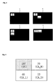
- FIG. 4 is a reference view for explaining a luminance contribution proportion of each unit area according to one embodiment of the present invention.
- FIG. 5 is a table showing a luminance contribution proportion of each unit area in FIG. 4 ;
- FIG. 6 is a table showing a luminance contribution percentage of each unit area in FIG. 4 ;
- FIG. 7 is a reference view for explaining a luminance contribution proportion of each unit area according to another embodiment of the present invention.
- FIG. 8 is a table showing a luminance contribution proportion of each unit area in FIG. 7 ;
- FIG. 9 is a table showing a luminance contribution percentage of each unit area in FIG. 7 ;
- FIG. 10 is a table showing types of unit areas according to one embodiment of the present invention.
- FIG. 11 is a flowchart illustrating a method for driving an LCD according to one embodiment of the present invention.
- FIG. 12 is a block diagram showing an LCD according to another embodiment of the present invention.
- the LCD includes an LCD panel 100 , a gate driver 110 , a source driver 120 , a timing controller 130 , a gamma voltage generating unit 140 , a luminance controller 150 , and a backlight unit 160 .
- the LCD panel 100 includes a plurality of gate and data lines arranged to cross each other. Also, a thin film transistor and a pixel electrode are disposed at each crossing of the gate and data lines, such that when scan signals are supplied through the gate lines and analog pixel signals are supplied through the data lines, images are displayed on the LCD panel 100 .
- the gate driver 110 sequentially supplies scan signals to the gate lines of the LCD panel 100
- the source driver 120 converts inputted pixel data into gamma voltages, namely, analog pixel signals, and supplies the gamma voltages to the data lines of the liquid crystal display panel 100 .
- the pixel data is digital signals representing gray levels set to have values within the range of 0 to 255
- the source driver 120 converts the pixel data using the gamma voltages of plural levels supplied from the gamma voltage generating unit 140 .
- the timing controller 130 supplies a timing control signal to the gate driver 110 and the source driver 120 , and also supplies the pixel data together with the timing control signal to the source driver 120 .
- the gamma voltage generating unit 140 generates suitable gamma voltages of plural levels according to transmission rate-voltage characteristics of the LCD panel 100 using a resistor group including a plurality of resistors arranged in series. The gamma voltages are controlled to have accurate and uniform values so that the LCD panel 100 can maintain a stable display quality when displaying images.
- the BLU 160 which as shown in FIG. 2 includes an LED array 161 , is installed on a rear surface of the LCD panel 100 and is divided into a plurality of unit areas (UA) so as to be sectionally driven to thereby irradiate light onto the LCD panel 100 .
- the LED array 161 includes a plurality of side radiation type LEDs 162 as shown in FIG. 3 . Also, the LEDs 162 belonging to each UA are controlled to be simultaneously turned on or off to thereby sectionally drive the BLU 160 by UAs.
- a luminance (brightness) of the LEDs 162 in the range of 0% to 100% is controlled according to a dimming operation of the luminance controller 150 .
- Three wavelength diodes of red, green and blue colors are used to implement various colors and increase the impression of colors.
- the luminance controller 150 receives the pixel data from the source driver 120 and mechanically or electronically controls a current according to the received pixel data to adjust a luminance of the LED array 161 by UAs. Namely, when an arbitrary UA is set as a reference UA, the luminance controller 150 detects pixel data of the reference UA and dims the LEDs 162 belonging to the reference UA according to the pixel data.
- the LEDs 162 are side radiation type LEDs 162 , light spreads largely to the side and a portion of light emitted upward also collides with and is reflected from a diverter 163 (see FIG. 3 ). Thus, the amount of light contributed by the LEDs 162 belonging to the arbitrary UA to the corresponding UA is relatively small compared with a top radiation type LED and luminance of the reference UA is affected by adjacent UAs.
- the luminance controller 150 controls a luminance of the LED array 161 using a luminance contribution percentage, namely, the percentage in which a luminance of the adjacent UAs that surround the reference UA affects the luminance of the reference UA.
- a luminance contribution percentage namely, the percentage in which a luminance of the adjacent UAs that surround the reference UA affects the luminance of the reference UA.
- the luminance controller 150 detects the brightest UA among the reference UA and the adjacent UAs, and if the reference UA is the brightest UA, the luminance controller 150 controls the reference UA to have an average luminance of pixel data corresponding to the reference UA.
- a correction luminance is calculated using a substantial luminance percentage, namely, the percentage in which the luminance of the reference UA is changed by the luminance of the adjacent UAs and the luminance contribution percentage of the adjacent UAs, and the reference UA is controlled to have the calculated correction luminance. Further, in sectionally driving the BLU 160 , a value of the average luminance of the reference UA and a value of the correction luminance that reflects the luminance contribution percentage of the adjacent UAs are compared and a greater value is determined as a dimming level of each UA constituting the BLU 160 .
- the luminance controller 150 serves as a rating mask so that, in a perceptional view point, UAs adjacent to a bright UA are turned on to be brighter in consideration of an influence of the bright UA, and thus, a boundary that may be generated due to the sectional driving of the BLU 160 is weakened.
- the reference screen (A) indicates an average luminance measured by driving only the LEDs 162 that belong to the reference UA (SA).
- the first to third luminance contribution proportion comparison screens (B, C and D) indicate an average luminance of the reference UA (SA) obtained by driving adjacent UAs (CA_D, CA_L, and CA_W) in diagonal, vertical and horizontal directions that surround the reference UA (SA), respectively, together with the reference UA (SA).
- the average luminance of the reference UA (SA) is measured to be 197 nit when only the LEDs 162 that belong to the reference UA (SA) are driven, if the diagonal, vertical and horizontal adjacent UAs (CA_D, CA_L, and CA_W) are driven to have a certain luminance value, the average luminance of the reference UA (SA) is changed to 220 nits, 243 nits, and 226 nits, respectively.
- FIG. 5 shows a table of the average luminance of the reference UA (SA) and each luminance contribution proportion of the adjacent UAs (CA_D, CA_L, and CA_W) to the reference UA (SA).
- each luminance contribution proportion is calculated as 23 nits (220-197), 46 nits (243-197), and 29 nits (226-197).
- FIG. 6 shows each luminance contribution percentage for determining whether to apply a correction luminance to the reference UA (SA) and a correction luminance calculated based on the results of FIG. 5 .
- the substantial luminance percentage of the reference UA (SA) and each luminance contribution percentage of the adjacent UAs (CA_D, CA_L, and CA_W) as shown in FIG. 6 are calculated based on the average luminance of the reference UA (SA) and the luminance contribution proportions of the adjacent UAs (CA_D, CA_L, and CA_W) as follows.
- the substantial luminance percentage of the reference UA (SA) is calculated as 66.78%[ ⁇ 197/(197+23+46+29) ⁇ *100] while the luminance contribution percentages of the respective adjacent UAs (CA_D, CA_L, and CA_W) are calculated as:
- the correction luminance of the reference UA can be calculated using the substantial luminance percentage of the reference UA (SA) and the luminance contribution percentages of the adjacent UAs (CA_D, CA_L, and CA_W) as ‘(197*0.6678+29*0.0983+46*0.1559+23*0.078/4’.
- the substantial luminance percentage of the reference UA (SA), the luminance contribution percentages of the adjacent UAs (CA_D, CA_L, and CA_W), and the correction luminance of the reference UA (SA) can be determined as follows.
- the substantial luminance percentage of the reference UA is obtained such that when the average luminance of the reference UA is controlled to have a first luminance value and the average luminance of the adjacent UAs (CA_D, CA_L, and CA_W) is controlled to have a second luminance value, an extent that the average luminance of the reference UA is changed is measured to be determined as the luminance contribution proportions of the adjacent UAs (CA_D, CA_L, and CA_W). Further, the ratio of the first luminance value to the sum of the first luminance value and the total obtained by adding up the luminance contribution proportions of the adjacent UAs (CA_D, CA_L, and CA_W) is expressed as the percentage.
- the luminance contribution percentages of the adjacent UAs are obtained such that when the average luminance of the reference unit area is controlled to have the first luminance value and the average luminance of the adjacent UAs (CA_D, CA_L, and CA_W) is controlled to have the second luminance value, an extent that the average luminance of the reference unit area is changed is measured to be determined as the luminance contribution proportions of the adjacent UAs (CA_D, CA_L, and CA_W), and the luminance contribution proportions of the adjacent UAs (CA_D, CA_L, and CA_W) to the sum of the first luminance value and the total obtained by adding up the luminance variation proportions of the adjacent UAs (CA_D, CA_L, and CA_W) are expressed as the percentage.
- the correction luminance of the reference UA is also obtained by dividing the sum of a value, which is obtained by multiplying the average luminance and the substantial luminance percentage of the reference UA, and a value, which is obtained by multiplying the average luminance and each luminance contribution percentage of the adjacent UAs (CA_D, CA_L, and CA_W), by the number of the adjacent UAs (CA_D, CA_L, and CA_W).
- FIG. 7 which illustrates the instance that when only the LEDs 162 that belong to the reference UA (SA) are driven, the average luminance of the reference UA (SA) is 216 nits, and as the LEDs 162 that belong to the diagonally, vertically and horizontally adjacent UAs (CA_D, CA_L, and CA_W) are driven to have a certain luminance value, the average luminance of the reference UA (SA) is changed to 236 nits, 273 nits, and 243 nits, respectively. Further, the average luminance and the substantial luminance percentage of the reference UA (SA) as shown in FIG. 9 are calculated based on the average luminance of the reference UA (SA) and the luminance contribution proportions of the respective adjacent UAs (CA_D, CA_L, and CA_W) as shown in FIG. 8 .
- the correction luminance of the reference UA is calculated as (20*0.0431*4+57*0.1228*2+27*0.0582*2+216*0.4655)/9 using the average luminance and the substantial luminance percentage of the reference UA (SA) and each luminance contribution percentage of the adjacent UAs (CA_D, CA_L, and CA_W).
- the correction luminance of the reference UA (SA) is determined according to the positions and number of the adjacent UAs (CA_D, CA_L, and CA_W). Namely, the positions and number of the adjacent UAs (CA_D, CA_L, and CA_W) are changed depending on where the reference UA (SA) is positioned. For example, if the reference UA (SA) is at an edge portion of the LCD panel 100 as shown in FIGS. 4 to 6 , the number of adjacent UAs (CA_D, CA_L, and CA_W) is 4, whereas if the reference UA (SA) is not on the edge portion of the liquid crystal display panel 100 as shown in FIGS. 7 to 9 , the number of adjacent UAs (CA_D, CA_L, and CA_W) used for calculating the corresponding luminance is 9.
- FIG. 10 is a table showing types of UAs according to one embodiment of the present invention, in which the number of adjacent UAs is different when calculating the correction luminance according to a position of the reference UA.
- the reference UAs can be divided into a type of reference UAs (UA 1 , UA 5 , UA 16 , and UA 20 ) that have one horizontally adjacent UA, one vertically adjacent UA, and one diagonally adjacent UA, a type of reference UAs (UA 2 , UA 3 , UA 4 , UA 17 , UA 18 , and UA 19 ) that have two horizontally adjacent UAs, one vertically adjacent UA, and two diagonally adjacent UA, a type of reference UAs (UA 6 , UA 10 , UA 11 , and UA 15 ) that have one horizontally adjacent UA, two vertically adjacent UAs, and two diagonally adjacent UAs, and a type of reference UAs (UA 7 , UA 8
- FIG. 11 is a flowchart illustrating a method for driving the LCD according to one embodiment of the present invention.
- FIG. 1 will also be referred to in this description.
- the timing controller 130 supplies timing control signals to the gate driver 110 and the source driver 120 , and supplies pixel data to the source driver 120 .
- the gate driver 110 sequentially supplies scan signals to the gate lines of the liquid crystal display panel 110 .
- the source driver 120 converts the pixel data into analog pixel signals and outputs the signals to the data lines of the LCD panel 100 .
- the luminance controller 150 receives the pixel data from the source driver, and controls a luminance of the side radiation type LED array 161 provided in the BLU 160 by the UAs according to the pixel data. The luminance of the LED array 161 is controlled using the luminance contribution percentage, namely, the ratio in which the luminance of the adjacent UAs that surround the reference UAs affects that of the reference UA.
- the luminance controller 150 detects the brightest UA among the reference UA and the adjacent UAs using the pixel data, and if the reference UA is the brightest area, the luminance controller 150 controls the reference UA to have an average luminance of corresponding pixel data. Meanwhile, if one or more of the adjacent UAs is/are brighter than the reference UA, the luminance controller calculates the correction luminance using the substantial luminance percentage of the reference UA and each luminance contribution percentage of the adjacent UAs and controls the reference UA to have the calculated correction luminance.
- the BLU 160 is sectionally driven by the plurality of UAs to irradiate light to the LCD panel 100 .
- the correction luminance of the reference UA, the substantial luminance percentage of the reference UA, and each luminance contribution percentage of the adjacent UAs are calculated as follows.
- the correction luminance of the reference UA is determined according to the positions and number of adjacent UAs, and preferably the correction luminance is calculated such that a value obtained by multiplying the average luminance and the substantial luminance percentage of the reference UA and a value obtained by multiplying the average luminance and the luminance contribution percentages of the respective adjacent UAs are added, and the sum is divided by the number of adjacent UAs to thereby obtain the correction luminance.
- the substantial luminance percentage of the reference unit area is obtained such that when the average luminance of the reference unit area is controlled to have a first luminance value and the average luminance of the adjacent unit areas is controlled to have a second luminance value, the extent that the average luminance of the reference unit area is changed is measured to be determined as the luminance contribution proportions of the adjacent unit areas, and the ratio of the first luminance value to the sum of the first luminance value and the total obtained by adding up the luminance contribution proportions of the adjacent unit areas is expressed as the percentage.
- the luminance contribution percentages of the adjacent unit areas are obtained such that when the average luminance of the reference unit area is controlled to have the first luminance value and the average luminance of the adjacent unit areas is controlled to have the second luminance value, the extent that the average luminance of the reference unit area is changed is measured to be determined as the luminance contribution proportions of the adjacent unit areas, and the luminance contribution proportions of the adjacent unit areas to the sum of the first luminance value and the total obtained by adding up the luminance variation proportions of the adjacent unit areas are expressed as the percentage.
- FIG. 12 is a block diagram showing of an LCD according to another embodiment of the present invention, which has a similar construction as that shown in FIG. 1 , except the luminance controller 150 receives pixel data from the timing controller 130 , and not from the source driver 120 .
- the timing controller 130 supplies a timing control signal to the gate driver 110 and the source driver 120 and pixel data to the luminance controller 150 .
- the luminance controller 150 receives the pixel data from the timing controller 130 and controls a current mechanically or electronically according to the received pixel data to control a luminance of the LED array 161 according to UAs.
- pixel data of the reference UA is sensed and the LEDs 162 that belong to the reference UA among the LED array 161 are dimmed according to the pixel data.
- the method for driving the LCD according to this embodiment is the same as the former embodiment, except that the luminance controller 150 receives pixel data from the timing controller 130 , and not from the source driver 120 as described above.
- the LCD according to the embodiments of the present invention can drive the side radiation type LEDs suitably according to sectional driving and enhance the efficiency and the contrast ratio of the liquid crystal display panel.
Abstract
Description
-
- 7.8%[{23/(197+23+46+29)}*100], 15.59%[{46/(197+23+46+29)}*100] and 9.83%[29/(197+23+46+29)], respectively.
Claims (14)
Applications Claiming Priority (2)
| Application Number | Priority Date | Filing Date | Title |
|---|---|---|---|
| KR10-2005-0057792 | 2005-06-30 | ||
| KR1020050057792A KR101169051B1 (en) | 2005-06-30 | 2005-06-30 | Liquid crystal display and method for driving the same |
Publications (2)
| Publication Number | Publication Date |
|---|---|
| US20070002000A1 US20070002000A1 (en) | 2007-01-04 |
| US7719512B2 true US7719512B2 (en) | 2010-05-18 |
Family
ID=37588863
Family Applications (1)
| Application Number | Title | Priority Date | Filing Date |
|---|---|---|---|
| US11/433,426 Expired - Fee Related US7719512B2 (en) | 2005-06-30 | 2006-05-15 | Liquid crystal display and method for driving the same |
Country Status (3)
| Country | Link |
|---|---|
| US (1) | US7719512B2 (en) |
| KR (1) | KR101169051B1 (en) |
| CN (1) | CN100514434C (en) |
Cited By (5)
| Publication number | Priority date | Publication date | Assignee | Title |
|---|---|---|---|---|
| US20090051907A1 (en) * | 2007-08-21 | 2009-02-26 | Au Optronics (Suzhou) Corp | Method for measuring brightness uniformity of a panel |
| US20090108761A1 (en) * | 2007-10-25 | 2009-04-30 | Yeo Dong-Min | Timing controller, liquid crystal display comprising the same and driving method of liquid crystal display |
| US20090189844A1 (en) * | 2008-01-24 | 2009-07-30 | Rohm Co., Ltd. | Back light system and liquid crystal display device using the back light system |
| US20110193889A1 (en) * | 2008-12-01 | 2011-08-11 | Sharp Kabushiki Kaisha | Backlight unit, liquid crystal display device, data generating method, data generating program and recording medium |
| US20200202798A1 (en) * | 2018-12-24 | 2020-06-25 | Lincoln Technology Solutions, Inc. | Video Pipeline Pixel Analysis for Full Array Local Dimming |
Families Citing this family (39)
| Publication number | Priority date | Publication date | Assignee | Title |
|---|---|---|---|---|
| JP5176397B2 (en) * | 2006-06-01 | 2013-04-03 | ソニー株式会社 | Display device and driving method thereof |
| US8228272B2 (en) * | 2006-12-22 | 2012-07-24 | Hong Kong Applied Science And Technlogy Research Institute Company Limited | Backlight device and liquid crystal display incorporating the backlight device |
| US8139022B2 (en) * | 2007-05-08 | 2012-03-20 | Victor Company Of Japan, Limited | Liquid crystal display device and image display method thereof |
| KR100885285B1 (en) * | 2007-05-08 | 2009-02-23 | 닛뽕빅터 가부시키가이샤 | Liquid crystal display apparatus and image display method used therein |
| US8207931B2 (en) * | 2007-05-31 | 2012-06-26 | Hong Kong Applied Science and Technology Research Institute Company Limited | Method of displaying a low dynamic range image in a high dynamic range |
| JP5110355B2 (en) * | 2007-07-09 | 2012-12-26 | Nltテクノロジー株式会社 | Backlight driving method and apparatus for liquid crystal display device, and liquid crystal display device |
| KR100867104B1 (en) * | 2007-07-27 | 2008-11-06 | 전자부품연구원 | Method and apparatus for controlling brightness of back light |
| JP4956520B2 (en) * | 2007-11-13 | 2012-06-20 | ミツミ電機株式会社 | Backlight device and liquid crystal display device using the same |
| US8104945B2 (en) * | 2007-12-27 | 2012-01-31 | Samsung Led Co., Ltd. | Backlight unit implementing local dimming for liquid crystal display device |
| KR100921518B1 (en) * | 2008-01-10 | 2009-10-12 | (주)다윈텍 | Led backlight system |
| KR101492116B1 (en) * | 2008-01-24 | 2015-02-09 | 삼성디스플레이 주식회사 | A connector and display device havine the same |
| JP5217586B2 (en) * | 2008-04-11 | 2013-06-19 | ソニー株式会社 | Display control apparatus and method, and program |
| KR101604652B1 (en) | 2008-06-04 | 2016-03-21 | 삼성디스플레이 주식회사 | Local dimming method of light source, light-source apparatus performing for the method and display apparatus having the light-source apparatus |
| KR100950682B1 (en) * | 2008-07-24 | 2010-03-31 | 전자부품연구원 | Apparatus and method for compensating brightness of back light |
| TW201005716A (en) * | 2008-07-24 | 2010-02-01 | Applied Green Light Taiwan Inc | Electronic display module and displaying method |
| US20100045190A1 (en) * | 2008-08-20 | 2010-02-25 | White Electronic Designs Corporation | Led backlight |
| JP4968219B2 (en) * | 2008-09-18 | 2012-07-04 | 株式会社Jvcケンウッド | Liquid crystal display device and video display method used therefor |
| EP2224422A4 (en) * | 2008-09-29 | 2012-04-18 | Panasonic Corp | Backlight device and display device |
| KR101539575B1 (en) * | 2009-01-28 | 2015-07-31 | 삼성디스플레이 주식회사 | Method of driving light-source, light-source apparatus performing for the method and display apparatus having the light-source apparatus |
| KR101598393B1 (en) | 2009-06-08 | 2016-03-02 | 삼성디스플레이 주식회사 | Method of dimming a light source and display apparatus for performing the method |
| KR101581427B1 (en) * | 2009-06-30 | 2015-12-31 | 삼성디스플레이 주식회사 | Display apparatus and method of driving the same |
| KR101351414B1 (en) * | 2009-12-14 | 2014-01-23 | 엘지디스플레이 주식회사 | Method for driving local dimming of liquid crystal display device using the same and apparatus thereof |
| CN102117600A (en) * | 2010-01-04 | 2011-07-06 | 青岛海信电器股份有限公司 | Method for improving partitioned halation of LED (Light Emitting Diode) backlight source and control device thereof |
| JP5661336B2 (en) * | 2010-05-28 | 2015-01-28 | 日立マクセル株式会社 | Liquid crystal display |
| CN101894519B (en) * | 2010-07-07 | 2013-01-23 | 深圳超多维光电子有限公司 | Data conversion device, data conversion method and data conversion system |
| WO2012124725A1 (en) * | 2011-03-15 | 2012-09-20 | シャープ株式会社 | Image signal processing device, display apparatus, television receiver, image signal processing method, and program |
| US9208730B2 (en) * | 2011-05-13 | 2015-12-08 | Samsung Display Co., Ltd. | Optimization of light source drive values in backlight systems |
| CN102768826B (en) * | 2011-07-27 | 2015-08-12 | 京东方科技集团股份有限公司 | A kind of scanning backlight method and device |
| TWI473071B (en) * | 2013-01-14 | 2015-02-11 | Novatek Microelectronics Corp | Display driving apparatus |
| CN103971647A (en) * | 2013-01-24 | 2014-08-06 | 联咏科技股份有限公司 | Display driver device |
| US9311863B2 (en) * | 2013-07-02 | 2016-04-12 | Novatek Microelectronics Corp. | Dimming method and dimming device for backlight module |
| CN103500566B (en) * | 2013-09-29 | 2016-10-05 | 京东方科技集团股份有限公司 | Display device, display brightness inequality improve device and ameliorative way |
| JP6368669B2 (en) * | 2015-03-17 | 2018-08-01 | ソニーセミコンダクタソリューションズ株式会社 | Display device and correction method |
| US10650758B2 (en) * | 2017-11-21 | 2020-05-12 | Wuhan China Star Optoelectronics Technology Co., Ltd. | Multi zone backlight controlling method and device thereof |
| GB2576060A (en) * | 2018-07-31 | 2020-02-05 | Continental Automotive Gmbh | Head-Up Display System |
| CN109119033B (en) * | 2018-10-17 | 2021-04-09 | 深圳Tcl新技术有限公司 | Backlight compensation method, device, system and storage medium |
| CN111383604B (en) * | 2018-12-27 | 2021-10-01 | 深圳Tcl新技术有限公司 | Method, system and storage medium for improving regional dimming algorithm |
| WO2022249311A1 (en) * | 2021-05-26 | 2022-12-01 | 三菱電機株式会社 | Display device and display method |
| CN115424594B (en) * | 2022-09-16 | 2023-03-28 | 北京显芯科技有限公司 | Data transmission method and controller |
Citations (3)
| Publication number | Priority date | Publication date | Assignee | Title |
|---|---|---|---|---|
| US20040257329A1 (en) * | 2003-06-20 | 2004-12-23 | Lg. Philips Lcd Co., Ltd. | Method and apparatus for driving liquid crystal display device |
| US20050248592A1 (en) * | 2004-05-04 | 2005-11-10 | Sharp Laboratories Of America, Inc. | Liquid crystal display with reduced black level insertion |
| US20060007111A1 (en) * | 2004-06-29 | 2006-01-12 | Lg.Philips Lcd Co., Ltd. | Liquid crystal display device having good image quality |
-
2005
- 2005-06-30 KR KR1020050057792A patent/KR101169051B1/en active IP Right Grant
-
2006
- 2006-05-15 US US11/433,426 patent/US7719512B2/en not_active Expired - Fee Related
- 2006-06-02 CN CNB2006100836678A patent/CN100514434C/en not_active Expired - Fee Related
Patent Citations (3)
| Publication number | Priority date | Publication date | Assignee | Title |
|---|---|---|---|---|
| US20040257329A1 (en) * | 2003-06-20 | 2004-12-23 | Lg. Philips Lcd Co., Ltd. | Method and apparatus for driving liquid crystal display device |
| US20050248592A1 (en) * | 2004-05-04 | 2005-11-10 | Sharp Laboratories Of America, Inc. | Liquid crystal display with reduced black level insertion |
| US20060007111A1 (en) * | 2004-06-29 | 2006-01-12 | Lg.Philips Lcd Co., Ltd. | Liquid crystal display device having good image quality |
Cited By (8)
| Publication number | Priority date | Publication date | Assignee | Title |
|---|---|---|---|---|
| US20090051907A1 (en) * | 2007-08-21 | 2009-02-26 | Au Optronics (Suzhou) Corp | Method for measuring brightness uniformity of a panel |
| US8208018B2 (en) * | 2007-08-21 | 2012-06-26 | Au Optronics (Suzhou) Corp | Method for measuring brightness uniformity of a panel |
| US20090108761A1 (en) * | 2007-10-25 | 2009-04-30 | Yeo Dong-Min | Timing controller, liquid crystal display comprising the same and driving method of liquid crystal display |
| US7995028B2 (en) * | 2007-10-25 | 2011-08-09 | Samsung Electronics Co., Ltd. | Timing controller, liquid crystal display comprising the same and driving method of liquid crystal display |
| US20090189844A1 (en) * | 2008-01-24 | 2009-07-30 | Rohm Co., Ltd. | Back light system and liquid crystal display device using the back light system |
| US8154507B2 (en) * | 2008-01-24 | 2012-04-10 | Rohm Co., Ltd. | Back light system and liquid crystal display device using the back light system |
| US20110193889A1 (en) * | 2008-12-01 | 2011-08-11 | Sharp Kabushiki Kaisha | Backlight unit, liquid crystal display device, data generating method, data generating program and recording medium |
| US20200202798A1 (en) * | 2018-12-24 | 2020-06-25 | Lincoln Technology Solutions, Inc. | Video Pipeline Pixel Analysis for Full Array Local Dimming |
Also Published As
| Publication number | Publication date |
|---|---|
| CN1892784A (en) | 2007-01-10 |
| KR101169051B1 (en) | 2012-07-26 |
| US20070002000A1 (en) | 2007-01-04 |
| KR20070002313A (en) | 2007-01-05 |
| CN100514434C (en) | 2009-07-15 |
Similar Documents
| Publication | Publication Date | Title |
|---|---|---|
| US7719512B2 (en) | Liquid crystal display and method for driving the same | |
| US8040317B2 (en) | Backlight device having LEDs controlled as a function of target values and influential extent data | |
| US8026893B2 (en) | Liquid crystal display device and apparatus and method for driving the same | |
| JP5368465B2 (en) | Power control method for light emitting device for image display, light emitting device for image display, display device, and television receiver | |
| JP5070331B2 (en) | LIGHTING DEVICE AND DISPLAY DEVICE HAVING THE SAME | |
| KR101295882B1 (en) | Liquid crystal display and local dimming control method of thereof | |
| US8358293B2 (en) | Method for driving light source blocks, driving unit for performing the method and display apparatus having the driving unit | |
| US9595229B2 (en) | Local dimming method and liquid crystal display | |
| US20100013866A1 (en) | Light source device and liquid crystal display unit | |
| JP4882657B2 (en) | Backlight control device, backlight control method, and liquid crystal display device | |
| US8766893B2 (en) | Method for compensating for poor uniformity of liquid crystal display having non-uniform backlight and display that exhibits non-uniformity compensating function | |
| US9852700B2 (en) | Liquid crystal display and method for driving the same | |
| US20090115720A1 (en) | Liquid crystal display, liquid crystal display module, and method of driving liquid crystal display | |
| US20100097412A1 (en) | Light source device and liquid crystal display unit | |
| US20100123743A1 (en) | Method of driving a light source, light source apparatus for performing the method and display apparatus having the light source apparatus | |
| US8274471B2 (en) | Liquid crystal display device and method for driving the same | |
| US8400394B2 (en) | Backlight unit assembly, liquid crystal display having the same, and dimming method thereof | |
| KR101327835B1 (en) | Driving circuit for liquid crystal display device and method for driving the same | |
| JP7222835B2 (en) | Display device | |
| KR102658431B1 (en) | Backlight unit and Liquid Crystal Display using the same | |
| KR100637438B1 (en) | Liquid Crystal Display | |
| KR20110064742A (en) | Back light unit and method driving of the same | |
| KR20060073742A (en) | Liquid crystal display and controlling method of the same | |
| KR20050011902A (en) | The Liquid Crystal Display Device and the method for driving the same | |
| KR20060114473A (en) | Liquid crystal display device |
Legal Events
| Date | Code | Title | Description |
|---|---|---|---|
| AS | Assignment |
Owner name: LG.PHILIPS LCD CO., LTD.,KOREA, REPUBLIC OF Free format text: ASSIGNMENT OF ASSIGNORS INTEREST;ASSIGNOR:KWON, KYUNG JOON;REEL/FRAME:017926/0764 Effective date: 20060626 Owner name: LG.PHILIPS LCD CO., LTD., KOREA, REPUBLIC OF Free format text: ASSIGNMENT OF ASSIGNORS INTEREST;ASSIGNOR:KWON, KYUNG JOON;REEL/FRAME:017926/0764 Effective date: 20060626 |
|
| AS | Assignment |
Owner name: LG DISPLAY CO., LTD., KOREA, REPUBLIC OF Free format text: CHANGE OF NAME;ASSIGNOR:LG.PHILIPS LCD CO., LTD.;REEL/FRAME:020985/0675 Effective date: 20080304 Owner name: LG DISPLAY CO., LTD.,KOREA, REPUBLIC OF Free format text: CHANGE OF NAME;ASSIGNOR:LG.PHILIPS LCD CO., LTD.;REEL/FRAME:020985/0675 Effective date: 20080304 |
|
| FEPP | Fee payment procedure |
Free format text: PAYOR NUMBER ASSIGNED (ORIGINAL EVENT CODE: ASPN); ENTITY STATUS OF PATENT OWNER: LARGE ENTITY |
|
| STCF | Information on status: patent grant |
Free format text: PATENTED CASE |
|
| FPAY | Fee payment |
Year of fee payment: 4 |
|
| MAFP | Maintenance fee payment |
Free format text: PAYMENT OF MAINTENANCE FEE, 8TH YEAR, LARGE ENTITY (ORIGINAL EVENT CODE: M1552) Year of fee payment: 8 |
|
| FEPP | Fee payment procedure |
Free format text: MAINTENANCE FEE REMINDER MAILED (ORIGINAL EVENT CODE: REM.); ENTITY STATUS OF PATENT OWNER: LARGE ENTITY |
|
| LAPS | Lapse for failure to pay maintenance fees |
Free format text: PATENT EXPIRED FOR FAILURE TO PAY MAINTENANCE FEES (ORIGINAL EVENT CODE: EXP.); ENTITY STATUS OF PATENT OWNER: LARGE ENTITY |
|
| STCH | Information on status: patent discontinuation |
Free format text: PATENT EXPIRED DUE TO NONPAYMENT OF MAINTENANCE FEES UNDER 37 CFR 1.362 |
|
| STCH | Information on status: patent discontinuation |
Free format text: PATENT EXPIRED DUE TO NONPAYMENT OF MAINTENANCE FEES UNDER 37 CFR 1.362 |
|
| FP | Lapsed due to failure to pay maintenance fee |
Effective date: 20220518 |