US7714327B2 - Electronic device improved in heat radiation performance for heat generated from active element - Google Patents
Electronic device improved in heat radiation performance for heat generated from active element Download PDFInfo
- Publication number
- US7714327B2 US7714327B2 US11/508,452 US50845206A US7714327B2 US 7714327 B2 US7714327 B2 US 7714327B2 US 50845206 A US50845206 A US 50845206A US 7714327 B2 US7714327 B2 US 7714327B2
- Authority
- US
- United States
- Prior art keywords
- thin film
- substrate
- electronic device
- thermal conductivity
- power consumption
- Prior art date
- Legal status (The legal status is an assumption and is not a legal conclusion. Google has not performed a legal analysis and makes no representation as to the accuracy of the status listed.)
- Active, expires
Links
Images


Classifications
-
- G—PHYSICS
- G02—OPTICS
- G02F—OPTICAL DEVICES OR ARRANGEMENTS FOR THE CONTROL OF LIGHT BY MODIFICATION OF THE OPTICAL PROPERTIES OF THE MEDIA OF THE ELEMENTS INVOLVED THEREIN; NON-LINEAR OPTICS; FREQUENCY-CHANGING OF LIGHT; OPTICAL LOGIC ELEMENTS; OPTICAL ANALOGUE/DIGITAL CONVERTERS
- G02F1/00—Devices or arrangements for the control of the intensity, colour, phase, polarisation or direction of light arriving from an independent light source, e.g. switching, gating or modulating; Non-linear optics
- G02F1/01—Devices or arrangements for the control of the intensity, colour, phase, polarisation or direction of light arriving from an independent light source, e.g. switching, gating or modulating; Non-linear optics for the control of the intensity, phase, polarisation or colour
- G02F1/13—Devices or arrangements for the control of the intensity, colour, phase, polarisation or direction of light arriving from an independent light source, e.g. switching, gating or modulating; Non-linear optics for the control of the intensity, phase, polarisation or colour based on liquid crystals, e.g. single liquid crystal display cells
- G02F1/133—Constructional arrangements; Operation of liquid crystal cells; Circuit arrangements
- G02F1/1333—Constructional arrangements; Manufacturing methods
- G02F1/1345—Conductors connecting electrodes to cell terminals
- G02F1/13454—Drivers integrated on the active matrix substrate
-
- G—PHYSICS
- G02—OPTICS
- G02F—OPTICAL DEVICES OR ARRANGEMENTS FOR THE CONTROL OF LIGHT BY MODIFICATION OF THE OPTICAL PROPERTIES OF THE MEDIA OF THE ELEMENTS INVOLVED THEREIN; NON-LINEAR OPTICS; FREQUENCY-CHANGING OF LIGHT; OPTICAL LOGIC ELEMENTS; OPTICAL ANALOGUE/DIGITAL CONVERTERS
- G02F1/00—Devices or arrangements for the control of the intensity, colour, phase, polarisation or direction of light arriving from an independent light source, e.g. switching, gating or modulating; Non-linear optics
- G02F1/01—Devices or arrangements for the control of the intensity, colour, phase, polarisation or direction of light arriving from an independent light source, e.g. switching, gating or modulating; Non-linear optics for the control of the intensity, phase, polarisation or colour
- G02F1/13—Devices or arrangements for the control of the intensity, colour, phase, polarisation or direction of light arriving from an independent light source, e.g. switching, gating or modulating; Non-linear optics for the control of the intensity, phase, polarisation or colour based on liquid crystals, e.g. single liquid crystal display cells
- G02F1/133—Constructional arrangements; Operation of liquid crystal cells; Circuit arrangements
- G02F1/1333—Constructional arrangements; Manufacturing methods
- G02F1/133382—Heating or cooling of liquid crystal cells other than for activation, e.g. circuits or arrangements for temperature control, stabilisation or uniform distribution over the cell
-
- H—ELECTRICITY
- H01—ELECTRIC ELEMENTS
- H01L—SEMICONDUCTOR DEVICES NOT COVERED BY CLASS H10
- H01L27/00—Devices consisting of a plurality of semiconductor or other solid-state components formed in or on a common substrate
- H01L27/02—Devices consisting of a plurality of semiconductor or other solid-state components formed in or on a common substrate including semiconductor components specially adapted for rectifying, oscillating, amplifying or switching and having at least one potential-jump barrier or surface barrier; including integrated passive circuit elements with at least one potential-jump barrier or surface barrier
- H01L27/12—Devices consisting of a plurality of semiconductor or other solid-state components formed in or on a common substrate including semiconductor components specially adapted for rectifying, oscillating, amplifying or switching and having at least one potential-jump barrier or surface barrier; including integrated passive circuit elements with at least one potential-jump barrier or surface barrier the substrate being other than a semiconductor body, e.g. an insulating body
Definitions
- the present invention relates to an electronic device having thin film active elements such as thin film transistors, thin film diodes etc.
- Japanese Patent Application Laid-open 2004-219551 (to be referred to hereinbelow as patent document 1) has proposed a flexible electronic device which is formed by thinning a glass substrate formed with a thin film transistor circuit to be greater than 0 ⁇ m to 200 ⁇ m in thickness, then by applying a transparent resin film or metal film over its entire surface.
- the reason for applying a metal film is to efficiently radiate heat from the self-heating of the device such as thin film transistors etc., to thereby prevent degradation of the device characteristics due to increased temperatures.
- Japanese Patent Application Laid-open H11-177102 (to be referred to hereinbelow as patent document 2) has proposed as a structure a thin film transistor device on a glass substrate, in which the size of a silicon active layer is made large so that it functions as a heat sinker to thereby discharge heat in an efficient manner.
- Japanese Patent Application Laid-open 2000-137211 (to be referred to hereinbelow as patent document 3) has also disclosed as a technique a thin film transistor liquid crystal display device on a glass substrate, in which large-sized metal heat-radiating pattern elements are connected to the thin film transistor circuits disposed around the substrate so as to enhance the effect of heat radiation.
- Japanese Patent Application Laid-open 2001-298169 discloses a technique for an improved heat radiation effect by forming a thin film transistor device on a sapphire substrate having a higher thermal conductivity than glass.
- patent document 2 and patent document 3 achieve efficient heat radiation by manipulating the structure of the thin film transistor device on the glass substrate.
- these techniques entail at least two problems. The first is that the size of the thin film transistor device becomes large, hence making it difficult to achieve high integration. Secondly, since the heat sink pattern elements have to be formed outside the thin film transistor array region, extra areas and processes are required.
- the object of the present invention is to provide an electronic device having improved heat radiation performance for heat generated from thin film active elements.
- an electronic device comprises a first substrate having a thickness of 200 ⁇ m or lower with a thin film active element having a maximum power consumption of 0.01 to 1 mW formed thereon, and a second substrate being applied to one surface of the two surfaces of said first substrate, the surface being the side other than that formed with said thin film active element, wherein a high thermal conductivity portion as a region whose thermal conductivity falls within the range from 0.1 to 4 W/cm ⁇ deg is provided in correspondence to the position of said thin film active element.
- a first substrate formed with a thin film active element having a maximum power consumption of 0.01 to 1 mW is applied to a second substrate, in which a region whose thermal conductivity falls within the range from 0.1 to 4 W/cm ⁇ deg is provided in correspondence to the position of the thin film active element. Accordingly, heat generated from the device can be radiated through a high thermal conductivity portion of the second substrate.
- FIGS. 1A , 1 B and 1 C are perspective views showing a structure of an electronic device in the first embodiment of the present invention
- FIGS. 2A , 2 B and 2 C are perspective views showing a structure of an electronic device in the second embodiment of the present invention.
- FIGS. 3A , 3 B and 3 C are perspective views showing a structure of an electronic device in the third embodiment of the present invention.
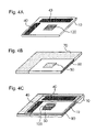
- FIGS. 4A , 4 B and 4 C are perspective views showing a structure of an electronic device in the fourth embodiment of the present invention.
- FIGS. 5A , 5 B and 5 C are perspective views showing a structure of an electronic device in the fifth embodiment of the present invention.
- FIGS. 6A , 6 B and 6 C are perspective views showing a structure of an electronic device in the sixth embodiment of the present invention.
- FIGS. 7A , 7 B and 7 C are perspective views showing a structure of an electronic device in the seventh embodiment of the present invention.
- FIG. 8 is a schematic sectional view showing a structure of an electronic device in the eighth embodiment of the present invention.
- An electronic device of the present invention is characterized by inclusion of a substrate having a region excellent in heat radiation performance formed in correspondence to the locations that have thin film active elements with high power consumption.
- FIGS. 1A to 1C are perspective views showing a structure of an electronic device of the present embodiment.
- FIG. 1A shows an array substrate on which a plurality of thin film transistors are formed;
- FIG. 1B shows a support substrate; and
- FIG. 1C shows an electronic device of the present embodiment.
- insulative substrate 10 having a thickness greater than 0 ⁇ m to 200 ⁇ m or lower, in the array substrate, are thin film transistors 20 arranged matrix-wise with matrix interconnections 30 and peripheral drive circuit portions 40 for driving thin film transistors 20 arranged matrix-wise.
- Peripheral drive circuit portion 40 is formed with a thin film transistor array (not shown) having a plurality of thin film transistors aligned thereon.
- Peripheral drive circuit portion 40 includes a shift register, a digital-analog conversion circuit (DAC circuit) and a power supply circuit.
- the region of peripheral drive circuit portion 40 includes thin film transistor elements having a maximum instantaneous power consumption of 0.05 mW or greater.
- Thin film transistors 20 arranged-matrix-wise are also laid out in an array-wise arrangement, but the maximum value of the power consumption as a single item is too low to consider, compared to that of peripheral drive circuit portion 40 .
- the support substrate shown in FIG. 1B is composed of high thermal conductivity portion 50 whose material is a thermal conductivity greater than 0.1 W/cm ⁇ deg and support base 60 as a part having an arbitrary thermal conductivity.
- thermal conductivity was specified to be 0.01 W/cm ⁇ deg (normal glass substrate), experimental data indicating degradation in device characteristics was obtained.
- thermal conductivity was specified to be 1.0 to 4.0 W/cm ⁇ deg (e.g., metal film substrate), degradation of the device characteristics was too small to matter.
- the thermal conductivity of high thermal conductivity portion 50 needs to be set within the range from 0.1 to 4 W/cm ⁇ deg. Further, to achieve more efficient heat radiation, the thermal conductivity of high thermal conductivity portion 50 preferably falls within the range of 0.5 to 4 W/cm ⁇ deg.
- the electronic device of the present embodiment has an array substrate shown in FIG. 1A and a support substrate shown in FIG. 1B , and is configured so that these two substrates are applied one over the other.
- the region of the support substrate of FIG. 1B located under the regions formed with peripheral drive circuit portions 40 is high thermal conductivity portion 50 consisting of a material whose thermal conductivity falls within the range of 0.1 to 4 W/cm ⁇ deg.
- an active matrix substrate for liquid crystal display will be explained.
- insulative substrate 10 a glass substrate having a thickness of 30 ⁇ m is used as insulative substrate 10 .
- a silicon thin film transistor is used as thin film transistor 20 .
- An aluminum interconnection is used as matrix interconnection 30 .
- Peripheral drive circuit portion 40 includes a shift register made up of a silicon thin film transistor array, a digital-analog conversion circuit (DAC circuit), a power supply circuit, a buffer, an analog switching circuit and the like.
- DAC circuit digital-analog conversion circuit
- a copper film having a thermal conductivity of 4 W/cm ⁇ deg is used for high thermal conductivity portion 50 , and a transparent film having a transmittance of 70% or greater for visible light rays with wavelengths of 380 nm (violet) to 770 nm (red) is used as support base 60 .
- silicon thin film transistors, aluminum interconnections and peripheral drive circuit portions 40 are formed on a glass substrate having a thickness of 30 ⁇ m to produce a thin type glass thin film transistor substrate.
- Copper film and transparent film are cut beforehand in predetermined shapes and joined to each other using an adhesive or the like to prepare a support substrate shown in FIG. 1B . Then these two substrates are bonded one over the other by an adhesive or the like to thereby complete an active matrix substrate for a liquid crystal display having excellent heat radiation performance.
- the power consumption of a thin film transistor having a wide channel whose width was 20 ⁇ m in the analog switching circuit portion, was about 0.1 mW.
- the temperature of the circuit portion was measured using an infrared radiation thermometer, the temperature rise caused by Joule heat was suppressed at around 70 deg. C., and no degradation of the device characteristics was observed after a long period of operation.
- the same measurement was made with a standard, active matrix substrate formed on glass with a thickness of 0.5 mm, the temperature of the aforementioned circuit portion was elevated up to about 200 deg. C., and gradual degradation of the device characteristics was observed. From this result, it is understood that use of the present invention makes it possible to realize a highly reliable active matrix substrate that has excellent heat radiation performance.
- the array substrate formed with thin film active elements having a maximum power consumption of 0.01 to 1 mW is applied to the support substrate, and the support substrate is formed with a region whose thermal conductivity falls within a range from 0.1 to 4 W/cm ⁇ deg, corresponding to the thin film active elements. Accordingly, heat generated from the device can be sufficiently radiated through the high thermal conductivity portion of the support substrate.
- transparent film is used for the regions except for those regions having copper film.
- an optical functional film such as a polarization film, phase difference film or the like may also be used.
- material having a high thermal conductivity may be disposed only under the region where thin film transistors that have high power consumption, hence high are self-heating, are formed, while various kinds of functional materials such as transparent materials, optical materials having birefringence and polarization, may be arranged in the other regions. Accordingly, this embodiment can be applied to various kinds of electronic devices.
- a plurality of desired different materials are combined beforehand to form a single substrate, then the substrate is applied to the array substrate formed with thin film transistors.
- the glass substrate can be made large in size, so that a greater number of devices can be produced from one substrate, compared to that from the silicon wafer, hence it is possible to produce electronic devices having equivalent performance at low costs.
- silicone resin material which presents a relatively high thermal conductivity may be used for further improved heat radiation performance.
- the thickness of the film consisting of high thermal conductivity material needs to be 5 ⁇ m or greater. This is because, when the thickness is less than 5 ⁇ m, the device temperature rises to about 200 deg. C., causing degradation of the device characteristics. In effect, if the film has a thickness of 100 ⁇ m, a sufficient enough heat radiation effect can be obtained.
- the support substrate does not necessarily have to be formed of copper film or transparent film, but, for example a base formed of a metal plate having a thickness of about 0.5 mm and a glass plate or resin substrate having a thickness of about 0.5 mm may be applied to the thin-type glass thin film transistor substrate.
- copper film was used for high thermal conductivity portion 50
- a material that contains, as an insulative material, a filler for enhanced thermal conductivity namely, high thermal conductive filler may be used.
- FIGS. 2A to 2C are perspective views showing an electronic device structure of the present embodiment.
- An array substrate shown in FIG. 2A has a configuration similar to that of the array substrate shown in FIG. 1A , which was described in the first embodiment.
- a support substrate shown in FIG. 2B is composed of high thermal conductivity thin-film portion 70 that is covered with a thin film of a material whose thermal conductivity falls within the range of 0.1 to 4 W/cm ⁇ deg and support base 80 that is not covered therewith.
- This support substrate is larger in size than the array substrate of FIG. 2A .
- the electronic device of the present embodiment has an array substrate shown in FIG. 2A and a support substrate shown in FIG. 2B , and is configured so that these two substrates are applied one over the other.
- the surface of the region of the support substrate of FIG. 2B located under the region formed with peripheral drive circuit portions 40 is covered with a thin film consisting of a material whose thermal conductivity falls within the range of 0.1 to 4 W/cm ⁇ deg.
- high thermal conductivity thin-film portion 70 it includes peripheral portion 90 which will not overlap the array substrate of FIG. 2A .
- Joule heat generated in region 40 where high power consumption thin film transistors are integrated can be efficiently released from high thermal conductivity thin-film portion 70 through thin insulative substrate 10 .
- Joule heat is made to dissipate sideways so that heat will escape efficiently from the portion at peripheral portion 90 .
- the array substrate shown in FIG. 2A has the same configuration as that of example 1 except that a glass substrate of 100 ⁇ m thick is used as insulative substrate 10 .
- This substrate is called a thin film transistor substrate.
- support base 80 is an optical functional film.
- high thermal conductivity thin-film portion 70 is film formed by plating a nickel thin-film having a thermal conductivity of 1 W/cm ⁇ deg over the optical functional film surface.
- the thin-film in high thermal conductivity thin-film portion 70 may also be film formed at desired positions by a spraying method such as ink jet etc.
- silicon thin film transistors, aluminum interconnections and peripheral drive circuit portions 40 are formed on a glass substrate having a thickness of 100 ⁇ m to produce a thin film transistor substrate.
- Thin film transistors may be formed directly on a thin glass substrate.
- a nickel thin-film having a thickness of 3 ⁇ m is film formed by plating on the polarization film at the desired part to produce a support substrate shown in FIG. 2B .
- peripheral portion 90 is preferably extended outwards 1 mm or greater beyond the edge of the thin film transistor substrate.
- the array substrate formed with thin film active elements having a maximum power consumption of 0.01 to 1 mW is applied to the support substrate, and the support substrate is covered with a thin-film whose thermal conductivity falls within a range from 0.1 to 4 W/cm ⁇ deg, over the area corresponding to the thin film active elements. Accordingly, heat generated from the device can be sufficiently radiated through the high thermal conductivity thin-film, so that the same effect as in the first embodiment can be obtained. Similar to the first embodiment, various functional materials can be arranged in the support substrate in portions other than the area where high thermal conductivity thin-film is formed.
- a high thermal conductivity material film is previously formed on a desired region on a substrate of a certain material, then the substrate is applied to the array substrate formed with thin film transistors.
- silicone resin material which has relatively high thermal conductivity, may be used for further improved heat radiation performance.
- transparent film or phase difference film may be used.
- the film may have a transmittance of 70% or greater for visible light rays as in example 1.
- the temperature rise can be suppressed to 150 deg. C. or lower, so that it is possible to confirm the effect of maintaining reliability of the device characteristics. If the glass thickness exceeds 200 ⁇ m, heat builds up inside the glass so that the device is elevated in temperature up to about 200 deg. C., thus failing to obtain any radiation effect.
- the film thickness of high thermal conductivity thin-film portion 70 needs to be 0.1 ⁇ m or greater. With a thickness of less than 0.1 ⁇ m, the device temperature rises up to about 200 deg. C., causing degradation of the device characteristics. The thicker the thin-film, the greater radiation effect it can provide. However, because it takes a longer time to form film, this lowers the throughput and the result is that maximum thickness may be about 100 ⁇ m. If the film forming rate can be enhanced, the film thickness may be made greater.
- Peripheral portion 90 is preferably extended outwards with a sticking out distance of 1 mm or greater beyond the edge of the thin film transistor substrate. If the distance is smaller than 1 mm, the device will be elevated in temperature up to 200 deg. or higher in some cases depending on the power consumption of the thin film transistors. It is considered that a sufficient radiation effect can be obtained if the sticking out distance is as much as 5 mm.
- the sticking out distance beyond the edge of the substrate is defined as the distance of the line that is perpendicular to the side of the substrate and parallel to the substrate plane, from the edge of the substrate.
- the base of a glass plate or resin substrate having a thickness of about 0.5 mm, for example, with a metal thin-film formed at desired positions, may be applied to the thin-type glass thin film transistor substrate.
- the thin-film may be formed with a material that contains, as an insulative material, a filler for enhanced thermal conductivity, namely, high thermal conductive filler.
- a self-luminous element such as an EL (electro luminescence) element etc.
- support base 80 does not necessarily have to be transparent.
- FIGS. 3A to 3C are perspective views showing a structure of an electronic device of this embodiment.
- FIG. 3A shows an array substrate on which a plurality of thin film transistors are formed
- FIG. 3B shows a support substrate.
- FIG. 3C shows an electronic device of this embodiment, and the electronic device of this embodiment is composed of an array substrate shown in FIG. 3A and a support substrate shown in FIG. 3B applied one over the other.
- the peripheral drive circuit portions on the array substrate shown in FIG. 3A include high-power consumption portion 110 in which thin film transistors having a higher maximum power consumption than those in peripheral drive circuit portion 40 shown in FIG. 2A are included, and low-power consumption portion 100 in which thin film transistors having a lower maximum power consumption than those in peripheral drive circuit portion 40 are included.
- the thin film transistor, included in peripheral drive circuit portion 40 which is the standard for maximum power consumption, is referred to as a standard thin film transistor.
- high power consumption portion 110 is arranged in a region closer to the edge of the array substrate than low power consumption portion 100 .
- High power consumption portion 110 may be composed of a single thin film transistor in some cases and may be formed with multiple arrays having a plurality of thin film transistors in other cases.
- buffers, analog switching circuits and the like include thin film transistors having large channel widths and high power consumption, so that formation of these circuit components in the region closer to the substrate edge is effective for heat radiation.
- high power consumption portion 110 was defined to be a region in which thin film transistors having a higher maximum power consumption than those in low power consumption portion 100 are included, it is also possible to define high power consumption portion 110 as a region whose power consumption per unit area is greater than that of low power consumption portion 100 . Alternatively, it is also possible to define high power consumption portion 110 to be a region that has a higher power consumption per unit area than that of the low power consumption portion 100 if compared with the fixed area size. In any case, provision of high power consumption portion 110 at a position closer to the substrate edge makes it possible to achieve heat radiation more efficiently.
- the support substrate of the second embodiment was used, but the support substrate of the first embodiment may also be used instead.
- the configuration of an electronic device of the present embodiment will be described.
- the first to third embodiments were described taking examples where the present invention is applied to a display active matrix substrate on which thin film transistors having a maximum power consumption equal to or greater than a predetermined level are arranged around the substrate.
- thin film transistors having high power consumption are provided not only in the periphery of the substrate but also in arbitrary areas other the periphery.
- FIGS. 4A to 4C are perspective views showing a structure of an electronic device of this embodiment.
- FIG. 4A shows an array substrate on which a plurality of thin film transistors are formed
- FIG. 4B shows a support substrate.
- FIG. 4C shows an electronic device of this embodiment, and the electronic device of this embodiment is composed of an array substrate shown in FIG. 4A and a support substrate shown in FIG. 4B applied one over the other.
- the same components as those in the first embodiment and the second embodiment are allotted with the same reference numerals with detailed description omitted.
- thin film transistor array 120 having a higher power consumption equal to or higher than a predetermined level is provided in periphery and in an arbitrary area that is not part of the periphery.
- a single thin film transistor array 120 is provided, but more than one array may be formed.
- the support substrate is formed with high thermal conductivity portion 50 consisting of a material whose thermal conductivity falls within the range of 0.1 to 4 W/cm ⁇ deg, in the position corresponding to the area where thin film transistor array 120 is formed.
- the surface of support base 80 located under the region formed with peripheral drive circuit portions 40 is covered with high thermal conductivity thin-film 70 , a film material whose thermal conductivity falls within the range of 0.1 to 4 W/cm ⁇ deg.
- the array substrate shown in FIG. 4A and the support substrate shown in FIG. 4B are applied one over the other as shown in FIG. 4C , so that high thermal conductivity portion 50 is located under the region where thin film transistor array 120 is formed. Further, high thermal conductivity thin-film 70 is disposed under the region where peripheral drive circuit portions 40 are formed. In this way, the electronic device of the present embodiment combines configuration of the high thermal conductivity portion of the first embodiment with the high thermal conductivity thin-film portion of the second embodiment.
- heat arising from peripheral drive circuit portions 40 is released through high thermal conductivity thin-film portion 70 and heat arising from thin film transistor array 120 is released through high thermal conductivity portion 50 .
- temperature rise can be inhibited.
- FIGS. 5A to 5C are perspective views showing a structure of an electronic device of this embodiment.
- FIG. 5A shows an array substrate on which a plurality of thin film transistors are formed
- FIG. 5B shows a support substrate
- FIG. 5C shows an electronic device of this embodiment, and the electronic device of this embodiment is composed of an array substrate shown in FIG. 5A and a support substrate shown in FIG. 5B applied one over the other.
- the same components as those in the fourth embodiment are allotted with the same reference numerals with detailed description omitted.
- the electronic device of the present embodiment is configured so that the portion, where high thermal conductivity thin-film 70 in the periphery is formed in the fourth embodiment, is replaced with high thermal conductivity portion 50 consisting of a material whose thermal conductivity falls within the range of 0.1 to 4 W/cm ⁇ deg. Also in the electronic device of this embodiment, the same effect as in the fourth embodiment can be obtained.
- FIGS. 6A to 6C are perspective views showing a structure of an electronic device of this embodiment.
- FIG. 6A shows an array substrate on which a plurality of thin film transistors are formed
- FIG. 6B shows a support substrate
- FIG. 6C shows an electronic device of this embodiment, and the electronic device of this embodiment is composed of an array substrate shown in FIG. 6A and a support substrate shown in FIG. 6B applied one over the other.
- the same components as those in the fourth embodiment are allotted with the same reference numerals with detailed description omitted.
- high thermal conductivity thin-film portion 70 made of a film material whose thermal conductivity falls within the range from 0.1 to 4 W/cm ⁇ deg, not only in the periphery of the support substrate and but also in arbitrary regions other than the periphery.
- FIG. 6B the center and its vicinity of support base 80 are covered by high thermal conductivity thin-film portion 70 .
- the position of high thermal conductivity thin-film portion 70 at around the center of the support substrate corresponds to thin film transistor array 120 , as shown in FIG. 6A . In this case, heat generated from thin film transistor array 120 cannot escape sideways.
- the film thickness of high thermal conductivity thin-film portion 70 at around the center of the support substrate, shown in FIG. 6B is preferably 0.5 ⁇ m or greater.
- the film thickness of high thermal conductivity thin-film portion 70 may be specified at a desirable thickness depending on individual regions.
- An integrated circuit in which an arithmetic processing circuit is provided in the form of thin film transistor array 120 at the center of the array substrate, a power source circuit and a controller circuit that are formed as the thin film transistor arrays of peripheral drive circuit portions 40 , for example, may be considered as a possible electronic device of the present embodiment.
- the circuit portions such as an arithmetic processing circuit, a power source circuit, a controller circuit and the like, thin film transistors that consume high power are high density integrated. Provision of high thermal conductivity thin-film portion 70 underneath such circuit portions contributes to improvement of heat radiation performance.
- the portions other than these circuit portions may be formed with, for example a transparent resin substrate, glass substrate or the like, as required. Therefore, support base 80 may be formed of a transparent resin substrate, glass substrate or the like.
- peripheral drive circuit portion 40 it is not always necessary to include peripheral drive circuit portion 40 .
- the present invention exemplified in the above first to sixth embodiments can be applied to an electronic device including at least one of peripheral drive circuit portion 40 and thin film transistor array 120 located at around the center of the substrate.
- the surface of high thermal conductivity portion 50 and high thermal conductivity thin-film portion 70 does not necessarily have to be flat, but may have a surface roughness of the order of some thousands of angstroms to some microns. Use of such an unevenness structure makes the effective contact area for heat radiation larger than that of the flat structure, hence more efficient heat radiation can be expected.
- FIGS. 7A to 7C are perspective views showing a structure of an electronic device of this embodiment.
- FIG. 7A shows an array substrate on which a plurality of thin film transistors are formed
- FIG. 7B shows a support substrate
- FIG. 7C shows an electronic device of this embodiment, and the electronic device of this embodiment is composed of an array substrate shown in FIG. 7A and a support substrate shown in FIG. 7B applied one over the other.
- the same components as those in the first embodiment are allotted with the same reference numerals with detailed description omitted.
- the array substrate shown in FIG. 7A has the same configuration as the array substrate shown in FIG. 1A , described in the first embodiment.
- the entire surface of the substrate is formed with metal thin-film 130 . Coverage of the entire surface with a metal thin-film permits the whole surface to radiate heat from the array substrate, thus enhancing heat radiation. Further, the surface that is put in contact with the array substrate of FIG. 7A is formed with an uneven texture. Further, in the configuration shown in FIG. 7C , when uneven textures are formed between the two substrates as stated above, the effective contact area that contributes to heat radiation becomes greater than the case with flat textures, hence an improved heat radiation effect can be expected. It is also possible to expect a light diffusion effect from the uneven textures. Accordingly, use of the support substrate of FIG. 7B not only for heat radiation purposes but also for light reflection and light diffusion purposes enables application of the device to a high performance reflection type active matrix substrate for liquid crystal displays.
- FIG. 8 is a schematic sectional view showing a structure of an electronic device of this embodiment.
- FIG. 8 shows a case of a liquid crystal display device in which a peripheral drive circuit and a pixel drive circuit are formed with thin film transistors.
- Peripheral drive circuit portion 40 Formed on first glass substrate 140 a is peripheral drive circuit portion 40 and a pixel drive circuit having thin film transistors 20 .
- Peripheral drive circuit portion 40 includes one or more thin film transistors having a maximum power consumption of 0.01 to 1 mW.
- resin layer 170 Formed over the region of this peripheral drive circuit portion 40 is resin layer 170 consisting of an insulative material.
- a high thermal conductivity material whose thermal conductivity falls within the range from 0.1 to 4 W/cm ⁇ deg is formed over resin layer 170 .
- the layer of this high thermal conductivity material is called high-thermal conductivity layer 180 .
- An example of high-thermal conductivity layer 180 is a metal film.
- a light-permeable transparent conductive material may also be used as a material for the metal film.
- Further second glass substrate 140 b is formed opposite the first glass substrate 140 a surface on which the pixel drive circuit is formed.
- First glass substrate 140 a and second glass substrate 140 b are fixed with liquid crystal seal agent 150 .
- Liquid crystal 160 is sealed inside the space enclosed by first glass substrate 140 a , second glass substrate 140 b and liquid crystal seal agent 150 .
- resin layer 170 is laminated over peripheral drive circuit portion 40 with many thin film transistors having high power consumption formed thereon, and high-thermal conductivity layer 180 made of metal film etc., is laminated over it.
- acrylic resin having a thickness of some tens of microns is laminated as resin layer 170 , and copper foil as a metal film is applied on it.
- Use of this configuration enables the metal film to radiate heat that arises from self-heating of the thin film transistors of peripheral drive circuit portion 40 and is conveyed through resin layer 170 , thus making it possible to suppress temperature rise of the thin film transistors.
- the first to eighth embodiments were described referring to cases where thin film transistors are used as switching elements, but thin film diodes may be used instead.
Abstract
Description
Claims (10)
Priority Applications (1)
| Application Number | Priority Date | Filing Date | Title |
|---|---|---|---|
| US12/749,063 US7989805B2 (en) | 2005-08-23 | 2010-03-29 | Electronic device improved in heat radiation performance for heat generated from active element |
Applications Claiming Priority (2)
| Application Number | Priority Date | Filing Date | Title |
|---|---|---|---|
| JP2005241031A JP5167580B2 (en) | 2005-08-23 | 2005-08-23 | Electronic devices |
| JP2005-241031 | 2005-08-23 |
Related Child Applications (1)
| Application Number | Title | Priority Date | Filing Date |
|---|---|---|---|
| US12/749,063 Division US7989805B2 (en) | 2005-08-23 | 2010-03-29 | Electronic device improved in heat radiation performance for heat generated from active element |
Publications (2)
| Publication Number | Publication Date |
|---|---|
| US20070049061A1 US20070049061A1 (en) | 2007-03-01 |
| US7714327B2 true US7714327B2 (en) | 2010-05-11 |
Family
ID=37804867
Family Applications (2)
| Application Number | Title | Priority Date | Filing Date |
|---|---|---|---|
| US11/508,452 Active 2028-10-18 US7714327B2 (en) | 2005-08-23 | 2006-08-23 | Electronic device improved in heat radiation performance for heat generated from active element |
| US12/749,063 Active US7989805B2 (en) | 2005-08-23 | 2010-03-29 | Electronic device improved in heat radiation performance for heat generated from active element |
Family Applications After (1)
| Application Number | Title | Priority Date | Filing Date |
|---|---|---|---|
| US12/749,063 Active US7989805B2 (en) | 2005-08-23 | 2010-03-29 | Electronic device improved in heat radiation performance for heat generated from active element |
Country Status (2)
| Country | Link |
|---|---|
| US (2) | US7714327B2 (en) |
| JP (1) | JP5167580B2 (en) |
Cited By (1)
| Publication number | Priority date | Publication date | Assignee | Title |
|---|---|---|---|---|
| US20100133635A1 (en) * | 2008-11-28 | 2010-06-03 | Samsung Electronics Co., Ltd. | image sensor and image sensing system including the same |
Families Citing this family (3)
| Publication number | Priority date | Publication date | Assignee | Title |
|---|---|---|---|---|
| CN101257844A (en) | 2005-04-29 | 2008-09-03 | 范德比特大学 | System and methods of using image-guidance for providing an access to a cochlear of a living subject |
| KR101534823B1 (en) * | 2008-11-28 | 2015-07-09 | 삼성전자주식회사 | Image sensor and image sensing system including of the same |
| CN106990583B (en) * | 2017-04-27 | 2019-08-02 | 厦门天马微电子有限公司 | A kind of display panel and display device |
Citations (10)
| Publication number | Priority date | Publication date | Assignee | Title |
|---|---|---|---|---|
| JPH05206468A (en) | 1991-09-02 | 1993-08-13 | Fuji Xerox Co Ltd | Thin film transistor and its manufacture |
| JPH10123964A (en) | 1996-08-30 | 1998-05-15 | Sony Corp | Liquid crystal display device |
| JPH11177102A (en) | 1997-12-08 | 1999-07-02 | Semiconductor Energy Lab Co Ltd | Semiconductor device and its manufacture |
| JP2000137211A (en) | 1998-11-04 | 2000-05-16 | Matsushita Electric Ind Co Ltd | Liquid crystal display device |
| JP2001298169A (en) | 2000-04-13 | 2001-10-26 | Seiko Epson Corp | Semiconductor device and producing method therefor |
| US6654075B1 (en) * | 1999-05-13 | 2003-11-25 | International Business Machines Corporation | Liquid crystal display device and method for fabricating the same |
| JP2004219551A (en) | 2003-01-10 | 2004-08-05 | Nec Corp | Flexible electronic device and method of manufacturing the same |
| JP2004327872A (en) | 2003-04-28 | 2004-11-18 | Sony Corp | Thin film transistor, its manufacturing method, display device using the thin film transistor and its manufacturing method |
| JP2004349537A (en) | 2003-05-23 | 2004-12-09 | Renesas Technology Corp | Semiconductor device |
| US6849877B2 (en) * | 2001-06-20 | 2005-02-01 | Semiconductor Energy Laboratory Co., Ltd. | Light emitting device and method of manufacturing the same |
Family Cites Families (4)
| Publication number | Priority date | Publication date | Assignee | Title |
|---|---|---|---|---|
| JP2000214478A (en) * | 1999-01-22 | 2000-08-04 | Matsushita Electric Ind Co Ltd | Liquid crystal panel |
| JP3341719B2 (en) * | 1999-07-07 | 2002-11-05 | 日本電気株式会社 | Semiconductor circuit cooling device and display device using the same |
| JP4531923B2 (en) * | 2000-04-25 | 2010-08-25 | 株式会社半導体エネルギー研究所 | Semiconductor device |
| TW554398B (en) * | 2001-08-10 | 2003-09-21 | Semiconductor Energy Lab | Method of peeling off and method of manufacturing semiconductor device |
-
2005
- 2005-08-23 JP JP2005241031A patent/JP5167580B2/en active Active
-
2006
- 2006-08-23 US US11/508,452 patent/US7714327B2/en active Active
-
2010
- 2010-03-29 US US12/749,063 patent/US7989805B2/en active Active
Patent Citations (10)
| Publication number | Priority date | Publication date | Assignee | Title |
|---|---|---|---|---|
| JPH05206468A (en) | 1991-09-02 | 1993-08-13 | Fuji Xerox Co Ltd | Thin film transistor and its manufacture |
| JPH10123964A (en) | 1996-08-30 | 1998-05-15 | Sony Corp | Liquid crystal display device |
| JPH11177102A (en) | 1997-12-08 | 1999-07-02 | Semiconductor Energy Lab Co Ltd | Semiconductor device and its manufacture |
| JP2000137211A (en) | 1998-11-04 | 2000-05-16 | Matsushita Electric Ind Co Ltd | Liquid crystal display device |
| US6654075B1 (en) * | 1999-05-13 | 2003-11-25 | International Business Machines Corporation | Liquid crystal display device and method for fabricating the same |
| JP2001298169A (en) | 2000-04-13 | 2001-10-26 | Seiko Epson Corp | Semiconductor device and producing method therefor |
| US6849877B2 (en) * | 2001-06-20 | 2005-02-01 | Semiconductor Energy Laboratory Co., Ltd. | Light emitting device and method of manufacturing the same |
| JP2004219551A (en) | 2003-01-10 | 2004-08-05 | Nec Corp | Flexible electronic device and method of manufacturing the same |
| JP2004327872A (en) | 2003-04-28 | 2004-11-18 | Sony Corp | Thin film transistor, its manufacturing method, display device using the thin film transistor and its manufacturing method |
| JP2004349537A (en) | 2003-05-23 | 2004-12-09 | Renesas Technology Corp | Semiconductor device |
Non-Patent Citations (1)
| Title |
|---|
| Satoshi Inoue, et al, "Study of Degradation Phenomenon Due to a Combination of Contamination and Self-Heating in Poly-Si Thin Film Transistors Fabricated by a Low-Temperature Process", Jpn. J. Appl. Phys., vol. 42, (2003), pp. 4213-4217. |
Cited By (2)
| Publication number | Priority date | Publication date | Assignee | Title |
|---|---|---|---|---|
| US20100133635A1 (en) * | 2008-11-28 | 2010-06-03 | Samsung Electronics Co., Ltd. | image sensor and image sensing system including the same |
| US8487351B2 (en) * | 2008-11-28 | 2013-07-16 | Samsung Electronics Co., Ltd. | Image sensor and image sensing system including the same |
Also Published As
| Publication number | Publication date |
|---|---|
| US20070049061A1 (en) | 2007-03-01 |
| US20100176398A1 (en) | 2010-07-15 |
| JP2007057675A (en) | 2007-03-08 |
| JP5167580B2 (en) | 2013-03-21 |
| US7989805B2 (en) | 2011-08-02 |
Similar Documents
| Publication | Publication Date | Title |
|---|---|---|
| TWI360366B (en) | Oled display having thermally conductive backplate | |
| JP4555339B2 (en) | OLED display with electrodes | |
| EP3270415B1 (en) | Display backplate and manufacturing method therefor, and display device | |
| JP6105911B2 (en) | OLED display panel | |
| KR101084230B1 (en) | Organic light emitting diode display and method for manufacturing the same | |
| EP3547368B1 (en) | Electronic device | |
| US20230317736A1 (en) | Electronic device | |
| US7989805B2 (en) | Electronic device improved in heat radiation performance for heat generated from active element | |
| CN100435380C (en) | Organic electroluminescent device having supporting plate and method of fabricating the same | |
| KR101996653B1 (en) | Flat panel display device | |
| US11393959B2 (en) | Micro light-emitting diode device | |
| KR20190114738A (en) | Electronic device | |
| US20200259050A1 (en) | Micro light emitting device display apparatus | |
| TW200923871A (en) | Integrated display module | |
| KR20170002726A (en) | Circuit Device Emitting Heat and Backlight Unit Comprising Thereof | |
| JP2008084965A (en) | Electronic device, substrate for dissipating heat, and electronic equipment | |
| JP2005109254A (en) | Integrated circuit mounting substrate and display device equipped with same | |
| KR20110057675A (en) | Display device and method for menufacturing display device | |
| JP2002083907A (en) | Semiconductor device, board, liquid crystal display and plasma display using the same | |
| TWI690079B (en) | Micro semiconductor device structure | |
| US7998764B2 (en) | Solid-state light emitting display and fabrication method thereof | |
| US20230128273A1 (en) | Thin film transistor substrate and display module comprising same | |
| JP7245889B2 (en) | Display device | |
| CN111554697B (en) | Display substrate, preparation method thereof and display device | |
| JP2023174033A (en) | Circuit using three-dimensional wiring, and manufacture method therefor |
Legal Events
| Date | Code | Title | Description |
|---|---|---|---|
| AS | Assignment |
Owner name: NEC CORPORATION,JAPAN Free format text: ASSIGNMENT OF ASSIGNORS INTEREST;ASSIGNORS:TAKECHI, KAZUSHIGE;KANOU, HIROSHI;NAKATA, MITSURU;REEL/FRAME:018211/0254 Effective date: 20060818 Owner name: NEC CORPORATION, JAPAN Free format text: ASSIGNMENT OF ASSIGNORS INTEREST;ASSIGNORS:TAKECHI, KAZUSHIGE;KANOU, HIROSHI;NAKATA, MITSURU;REEL/FRAME:018211/0254 Effective date: 20060818 |
|
| STCF | Information on status: patent grant |
Free format text: PATENTED CASE |
|
| AS | Assignment |
Owner name: GOLD CHARM LIMITED, SAMOA Free format text: ASSIGNMENT OF ASSIGNORS INTEREST;ASSIGNOR:NEC CORPORATION;REEL/FRAME:030024/0921 Effective date: 20121130 |
|
| FPAY | Fee payment |
Year of fee payment: 4 |
|
| MAFP | Maintenance fee payment |
Free format text: PAYMENT OF MAINTENANCE FEE, 8TH YEAR, LARGE ENTITY (ORIGINAL EVENT CODE: M1552) Year of fee payment: 8 |
|
| MAFP | Maintenance fee payment |
Free format text: PAYMENT OF MAINTENANCE FEE, 12TH YEAR, LARGE ENTITY (ORIGINAL EVENT CODE: M1553); ENTITY STATUS OF PATENT OWNER: LARGE ENTITY Year of fee payment: 12 |
|
| AS | Assignment |
Owner name: HANNSTAR DISPLAY CORPORATION, TAIWAN Free format text: ASSIGNMENT OF ASSIGNORS INTEREST;ASSIGNOR:GOLD CHARM LIMITED;REEL/FRAME:063383/0154 Effective date: 20230320 |