US7714079B2 - Patternable low dielectric constant materials and their use in ULSI interconnection - Google Patents
Patternable low dielectric constant materials and their use in ULSI interconnection Download PDFInfo
- Publication number
- US7714079B2 US7714079B2 US11/933,530 US93353007A US7714079B2 US 7714079 B2 US7714079 B2 US 7714079B2 US 93353007 A US93353007 A US 93353007A US 7714079 B2 US7714079 B2 US 7714079B2
- Authority
- US
- United States
- Prior art keywords
- low
- acid
- film stack
- cured
- sensitive
- Prior art date
- Legal status (The legal status is an assumption and is not a legal conclusion. Google has not performed a legal analysis and makes no representation as to the accuracy of the status listed.)
- Expired - Fee Related
Links
- 0 [1*]C(C)C([2*])C Chemical compound [1*]C(C)C([2*])C 0.000 description 14
- ACEJATUPWDHDTM-UHFFFAOYSA-N C.C.C.C.C.C.C.C.C.C.C.C.C.C.C.C.C.C.C.C.C.C.C.C.C.C.C.C.C.C.C.C.C.C.C.C.CC(C)C(C)C(C(=O)O)C(F)(F)F.CC(C)C(C)c1ccc(O)cc1.CC(C)CCC(C)(O)C(F)(F)F.CC(CC(O)C(F)(F)F)C(C)C(C)c1ccc(O)cc1.CC(CCC(=O)O)C(C)C(C)c1ccc(O)cc1.CC(CCC(=O)OCCO)C(C)CC(C)(O)C(F)(F)F.CC(CCC(C)(O)C(F)(F)F)C(C)CC(O)C(F)(F)F.CC(CCc1ccc(C(C)(O)C(F)(F)F)cc1)C(C)CC(O)C(F)(F)F.CC(CCc1ccc(O)cc1)C(C)CC(O)C(F)(F)F.CC(CO)C(C)CCC(C)(O)C(F)(F)F.OC(CC1CC2CCC1C2)(C(F)(F)F)C(F)(F)F Chemical compound C.C.C.C.C.C.C.C.C.C.C.C.C.C.C.C.C.C.C.C.C.C.C.C.C.C.C.C.C.C.C.C.C.C.C.C.CC(C)C(C)C(C(=O)O)C(F)(F)F.CC(C)C(C)c1ccc(O)cc1.CC(C)CCC(C)(O)C(F)(F)F.CC(CC(O)C(F)(F)F)C(C)C(C)c1ccc(O)cc1.CC(CCC(=O)O)C(C)C(C)c1ccc(O)cc1.CC(CCC(=O)OCCO)C(C)CC(C)(O)C(F)(F)F.CC(CCC(C)(O)C(F)(F)F)C(C)CC(O)C(F)(F)F.CC(CCc1ccc(C(C)(O)C(F)(F)F)cc1)C(C)CC(O)C(F)(F)F.CC(CCc1ccc(O)cc1)C(C)CC(O)C(F)(F)F.CC(CO)C(C)CCC(C)(O)C(F)(F)F.OC(CC1CC2CCC1C2)(C(F)(F)F)C(F)(F)F ACEJATUPWDHDTM-UHFFFAOYSA-N 0.000 description 1
- KZNJUHBCNBUGRL-UHFFFAOYSA-N C=C(C(=O)O)C(F)(F)F.C=C(C(=O)OC)C(F)(F)F.C=C(C(=O)OCCO)C(F)(F)F.C=C(C)C(=O)OC(C)(C)C.C=C(C)C(=O)OCCO.C=C(F)F.C=C(OC(C)(C)C)C(=C)C(F)(F)F.C=CC(=O)OC(C)(C)C.C=CC1CCC(O)CC1.C=CC1CCCC2OC12.C=Cc1ccc(C(C)(O)C(F)(F)F)cc1.C=Cc1ccc(O)cc1.CC(=O)OC(CC1CC2C=CC1C2)(C(F)(F)F)C(F)(F)F.CC(CC1CC2C=CC1C2)(C(F)(F)F)C(F)(F)F.CFF.O=C(O)C1CC2C=CC1C2.O=C1C=CC(=O)O1.OC(CC1CC2C=CC1C2)(C(F)(F)F)C(F)(F)F.OC(F)(C1CC2C=CC1C2)C(F)(F)F Chemical compound C=C(C(=O)O)C(F)(F)F.C=C(C(=O)OC)C(F)(F)F.C=C(C(=O)OCCO)C(F)(F)F.C=C(C)C(=O)OC(C)(C)C.C=C(C)C(=O)OCCO.C=C(F)F.C=C(OC(C)(C)C)C(=C)C(F)(F)F.C=CC(=O)OC(C)(C)C.C=CC1CCC(O)CC1.C=CC1CCCC2OC12.C=Cc1ccc(C(C)(O)C(F)(F)F)cc1.C=Cc1ccc(O)cc1.CC(=O)OC(CC1CC2C=CC1C2)(C(F)(F)F)C(F)(F)F.CC(CC1CC2C=CC1C2)(C(F)(F)F)C(F)(F)F.CFF.O=C(O)C1CC2C=CC1C2.O=C1C=CC(=O)O1.OC(CC1CC2C=CC1C2)(C(F)(F)F)C(F)(F)F.OC(F)(C1CC2C=CC1C2)C(F)(F)F KZNJUHBCNBUGRL-UHFFFAOYSA-N 0.000 description 1
- DLMCKMKXLVMIGN-UHFFFAOYSA-N CC(=O)C1CC2CC(C)C1C2.CC(C)C1=CC=C(C(O)(C(F)(F)F)C(F)(F)F)C=C1.CC(C)C1=CC=C(O)C=C1.CC1CC2CC(CC(O)(C(F)(F)F)C(F)(F)F)C1C2.CC1CC2CC1C(C(O)(C(F)(F)F)C(F)(F)F)C2.CCC(C(=O)O)C(F)(F)F.CCC(C)C(=O)O.CCC(O)(C(F)(F)F)C(F)(F)F.CCC(O)C(F)(F)F.CCC1=CC=C(CC(O)(F)C(F)(F)F)C=C1.CCC1=CC=C(O)C=C1.CCCC(=O)O.CCCC(=O)OC(C1CCC(C(O)(C(F)(F)F)C(F)(F)F)CC1)(C(F)(F)F)C(F)(F)F.CCCC(O)(C(F)(F)F)C(F)(F)F.CCCC1=CC=C(C(O)(C(F)(F)F)C(F)(F)F)C=C1.CCCC1=CC=C(CC(O)(F)C(F)(F)F)C=C1.CCCC1=CC=C(O)C=C1.CFF.CFF Chemical compound CC(=O)C1CC2CC(C)C1C2.CC(C)C1=CC=C(C(O)(C(F)(F)F)C(F)(F)F)C=C1.CC(C)C1=CC=C(O)C=C1.CC1CC2CC(CC(O)(C(F)(F)F)C(F)(F)F)C1C2.CC1CC2CC1C(C(O)(C(F)(F)F)C(F)(F)F)C2.CCC(C(=O)O)C(F)(F)F.CCC(C)C(=O)O.CCC(O)(C(F)(F)F)C(F)(F)F.CCC(O)C(F)(F)F.CCC1=CC=C(CC(O)(F)C(F)(F)F)C=C1.CCC1=CC=C(O)C=C1.CCCC(=O)O.CCCC(=O)OC(C1CCC(C(O)(C(F)(F)F)C(F)(F)F)CC1)(C(F)(F)F)C(F)(F)F.CCCC(O)(C(F)(F)F)C(F)(F)F.CCCC1=CC=C(C(O)(C(F)(F)F)C(F)(F)F)C=C1.CCCC1=CC=C(CC(O)(F)C(F)(F)F)C=C1.CCCC1=CC=C(O)C=C1.CFF.CFF DLMCKMKXLVMIGN-UHFFFAOYSA-N 0.000 description 1
- BSAMIHNJQILJIF-UHFFFAOYSA-N CC(C)C1=CC=C(CC(O)(C(F)(F)F)C(F)(F)F)C=C1.CCC1=CC=C(CC(O)(C(F)(F)F)C(F)(F)F)C=C1.CCCC1=CC=C(CC(O)(C(F)(F)F)C(F)(F)F)C=C1.CCCC1=CC=C(O)C=C1 Chemical compound CC(C)C1=CC=C(CC(O)(C(F)(F)F)C(F)(F)F)C=C1.CCC1=CC=C(CC(O)(C(F)(F)F)C(F)(F)F)C=C1.CCCC1=CC=C(CC(O)(C(F)(F)F)C(F)(F)F)C=C1.CCCC1=CC=C(O)C=C1 BSAMIHNJQILJIF-UHFFFAOYSA-N 0.000 description 1
- ZWWLGVPFHQMJEH-UHFFFAOYSA-N CC.CC(C)C1=CC=C(C(O)(C(F)(F)F)C(F)(F)F)C=C1.CC(C)C1=CC=C(O)C=C1.CC1CC2CC(C(=O)O)C1C2.CC1CC2CC(CC(O)(C(F)(F)F)C(F)(F)F)C1C2.CCC(C(=O)O)C(F)(F)F.CCC(C)C(=O)O.CCC(O)(C(F)(F)F)C(F)(F)F.CCC(O)C(F)(F)F.CCC1=CC=C(CC(O)(F)C(F)(F)F)C=C1.CCC1=CC=C(O)C=C1.CCCC(=O)O.CCCC(=O)OC(C1CCC(C(O)(C(F)(F)F)C(F)(F)F)CC1)(C(F)(F)F)C(F)(F)F.CCCC(O)(C(F)(F)F)C(F)(F)F.CCCC1=CC=C(C(O)(C(F)(F)F)C(F)(F)F)C=C1.CCCC1=CC=C(CC(O)(F)C(F)(F)F)C=C1.CCCC1=CC=C(O)C=C1.CFF.CFF.OC(C1CC2CCC1C2)(C(F)(F)F)C(F)(F)F Chemical compound CC.CC(C)C1=CC=C(C(O)(C(F)(F)F)C(F)(F)F)C=C1.CC(C)C1=CC=C(O)C=C1.CC1CC2CC(C(=O)O)C1C2.CC1CC2CC(CC(O)(C(F)(F)F)C(F)(F)F)C1C2.CCC(C(=O)O)C(F)(F)F.CCC(C)C(=O)O.CCC(O)(C(F)(F)F)C(F)(F)F.CCC(O)C(F)(F)F.CCC1=CC=C(CC(O)(F)C(F)(F)F)C=C1.CCC1=CC=C(O)C=C1.CCCC(=O)O.CCCC(=O)OC(C1CCC(C(O)(C(F)(F)F)C(F)(F)F)CC1)(C(F)(F)F)C(F)(F)F.CCCC(O)(C(F)(F)F)C(F)(F)F.CCCC1=CC=C(C(O)(C(F)(F)F)C(F)(F)F)C=C1.CCCC1=CC=C(CC(O)(F)C(F)(F)F)C=C1.CCCC1=CC=C(O)C=C1.CFF.CFF.OC(C1CC2CCC1C2)(C(F)(F)F)C(F)(F)F ZWWLGVPFHQMJEH-UHFFFAOYSA-N 0.000 description 1
- WQMWMGDLFFBWFB-UHFFFAOYSA-N CCC(C(=O)OC(C)(C)C)C(F)(F)F.CCC(C)C(=O)OC(C)(C)C.CCCC(=O)OC(C)(C)C.CO[Si](C)(C)C(C)c1ccc(OC(=O)OC(C)(C)C)cc1.CO[Si](C)(C)C1CC2CC1CC2C(O)(C(F)(F)F)C(F)(F)F.CO[Si](C)(C)CCc1ccc(O)cc1 Chemical compound CCC(C(=O)OC(C)(C)C)C(F)(F)F.CCC(C)C(=O)OC(C)(C)C.CCCC(=O)OC(C)(C)C.CO[Si](C)(C)C(C)c1ccc(OC(=O)OC(C)(C)C)cc1.CO[Si](C)(C)C1CC2CC1CC2C(O)(C(F)(F)F)C(F)(F)F.CO[Si](C)(C)CCc1ccc(O)cc1 WQMWMGDLFFBWFB-UHFFFAOYSA-N 0.000 description 1
- UJBRYIQCSKHHHY-UHFFFAOYSA-N COCN(CC1=NC(N(COC)COC)=NC(N(COC)COC)=N1)OC.COCN1CCCN(COC)C1=O.COCN1CN(C)CN(COC)C1=O.COCN1COCN(COC)C1=O.[H]CC1=NC(N(C[H])OC)=NC(NCOC)=N1 Chemical compound COCN(CC1=NC(N(COC)COC)=NC(N(COC)COC)=N1)OC.COCN1CCCN(COC)C1=O.COCN1CN(C)CN(COC)C1=O.COCN1COCN(COC)C1=O.[H]CC1=NC(N(C[H])OC)=NC(NCOC)=N1 UJBRYIQCSKHHHY-UHFFFAOYSA-N 0.000 description 1
- GNBCQANWHPNGBC-UHFFFAOYSA-N CO[N]1(N)O[N](N)(ON(N)ON(N)OI)ON(N)ON(N)O1 Chemical compound CO[N]1(N)O[N](N)(ON(N)ON(N)OI)ON(N)ON(N)O1 GNBCQANWHPNGBC-UHFFFAOYSA-N 0.000 description 1
Images


Classifications
-
- G—PHYSICS
- G03—PHOTOGRAPHY; CINEMATOGRAPHY; ANALOGOUS TECHNIQUES USING WAVES OTHER THAN OPTICAL WAVES; ELECTROGRAPHY; HOLOGRAPHY
- G03F—PHOTOMECHANICAL PRODUCTION OF TEXTURED OR PATTERNED SURFACES, e.g. FOR PRINTING, FOR PROCESSING OF SEMICONDUCTOR DEVICES; MATERIALS THEREFOR; ORIGINALS THEREFOR; APPARATUS SPECIALLY ADAPTED THEREFOR
- G03F7/00—Photomechanical, e.g. photolithographic, production of textured or patterned surfaces, e.g. printing surfaces; Materials therefor, e.g. comprising photoresists; Apparatus specially adapted therefor
- G03F7/004—Photosensitive materials
- G03F7/075—Silicon-containing compounds
- G03F7/0757—Macromolecular compounds containing Si-O, Si-C or Si-N bonds
-
- G—PHYSICS
- G03—PHOTOGRAPHY; CINEMATOGRAPHY; ANALOGOUS TECHNIQUES USING WAVES OTHER THAN OPTICAL WAVES; ELECTROGRAPHY; HOLOGRAPHY
- G03F—PHOTOMECHANICAL PRODUCTION OF TEXTURED OR PATTERNED SURFACES, e.g. FOR PRINTING, FOR PROCESSING OF SEMICONDUCTOR DEVICES; MATERIALS THEREFOR; ORIGINALS THEREFOR; APPARATUS SPECIALLY ADAPTED THEREFOR
- G03F7/00—Photomechanical, e.g. photolithographic, production of textured or patterned surfaces, e.g. printing surfaces; Materials therefor, e.g. comprising photoresists; Apparatus specially adapted therefor
- G03F7/004—Photosensitive materials
- G03F7/075—Silicon-containing compounds
-
- C—CHEMISTRY; METALLURGY
- C08—ORGANIC MACROMOLECULAR COMPOUNDS; THEIR PREPARATION OR CHEMICAL WORKING-UP; COMPOSITIONS BASED THEREON
- C08G—MACROMOLECULAR COMPOUNDS OBTAINED OTHERWISE THAN BY REACTIONS ONLY INVOLVING UNSATURATED CARBON-TO-CARBON BONDS
- C08G77/00—Macromolecular compounds obtained by reactions forming a linkage containing silicon with or without sulfur, nitrogen, oxygen or carbon in the main chain of the macromolecule
- C08G77/04—Polysiloxanes
- C08G77/22—Polysiloxanes containing silicon bound to organic groups containing atoms other than carbon, hydrogen and oxygen
- C08G77/24—Polysiloxanes containing silicon bound to organic groups containing atoms other than carbon, hydrogen and oxygen halogen-containing groups
-
- C—CHEMISTRY; METALLURGY
- C09—DYES; PAINTS; POLISHES; NATURAL RESINS; ADHESIVES; COMPOSITIONS NOT OTHERWISE PROVIDED FOR; APPLICATIONS OF MATERIALS NOT OTHERWISE PROVIDED FOR
- C09D—COATING COMPOSITIONS, e.g. PAINTS, VARNISHES OR LACQUERS; FILLING PASTES; CHEMICAL PAINT OR INK REMOVERS; INKS; CORRECTING FLUIDS; WOODSTAINS; PASTES OR SOLIDS FOR COLOURING OR PRINTING; USE OF MATERIALS THEREFOR
- C09D183/00—Coating compositions based on macromolecular compounds obtained by reactions forming in the main chain of the macromolecule a linkage containing silicon, with or without sulfur, nitrogen, oxygen, or carbon only; Coating compositions based on derivatives of such polymers
- C09D183/04—Polysiloxanes
- C09D183/08—Polysiloxanes containing silicon bound to organic groups containing atoms other than carbon, hydrogen, and oxygen
-
- G—PHYSICS
- G03—PHOTOGRAPHY; CINEMATOGRAPHY; ANALOGOUS TECHNIQUES USING WAVES OTHER THAN OPTICAL WAVES; ELECTROGRAPHY; HOLOGRAPHY
- G03F—PHOTOMECHANICAL PRODUCTION OF TEXTURED OR PATTERNED SURFACES, e.g. FOR PRINTING, FOR PROCESSING OF SEMICONDUCTOR DEVICES; MATERIALS THEREFOR; ORIGINALS THEREFOR; APPARATUS SPECIALLY ADAPTED THEREFOR
- G03F7/00—Photomechanical, e.g. photolithographic, production of textured or patterned surfaces, e.g. printing surfaces; Materials therefor, e.g. comprising photoresists; Apparatus specially adapted therefor
- G03F7/004—Photosensitive materials
- G03F7/0046—Photosensitive materials with perfluoro compounds, e.g. for dry lithography
-
- H—ELECTRICITY
- H01—ELECTRIC ELEMENTS
- H01L—SEMICONDUCTOR DEVICES NOT COVERED BY CLASS H10
- H01L21/00—Processes or apparatus adapted for the manufacture or treatment of semiconductor or solid state devices or of parts thereof
- H01L21/02—Manufacture or treatment of semiconductor devices or of parts thereof
- H01L21/02104—Forming layers
- H01L21/02107—Forming insulating materials on a substrate
- H01L21/02109—Forming insulating materials on a substrate characterised by the type of layer, e.g. type of material, porous/non-porous, pre-cursors, mixtures or laminates
- H01L21/02112—Forming insulating materials on a substrate characterised by the type of layer, e.g. type of material, porous/non-porous, pre-cursors, mixtures or laminates characterised by the material of the layer
- H01L21/02118—Forming insulating materials on a substrate characterised by the type of layer, e.g. type of material, porous/non-porous, pre-cursors, mixtures or laminates characterised by the material of the layer carbon based polymeric organic or inorganic material, e.g. polyimides, poly cyclobutene or PVC
-
- H—ELECTRICITY
- H01—ELECTRIC ELEMENTS
- H01L—SEMICONDUCTOR DEVICES NOT COVERED BY CLASS H10
- H01L21/00—Processes or apparatus adapted for the manufacture or treatment of semiconductor or solid state devices or of parts thereof
- H01L21/02—Manufacture or treatment of semiconductor devices or of parts thereof
- H01L21/02104—Forming layers
- H01L21/02107—Forming insulating materials on a substrate
- H01L21/02109—Forming insulating materials on a substrate characterised by the type of layer, e.g. type of material, porous/non-porous, pre-cursors, mixtures or laminates
- H01L21/02112—Forming insulating materials on a substrate characterised by the type of layer, e.g. type of material, porous/non-porous, pre-cursors, mixtures or laminates characterised by the material of the layer
- H01L21/02123—Forming insulating materials on a substrate characterised by the type of layer, e.g. type of material, porous/non-porous, pre-cursors, mixtures or laminates characterised by the material of the layer the material containing silicon
- H01L21/02126—Forming insulating materials on a substrate characterised by the type of layer, e.g. type of material, porous/non-porous, pre-cursors, mixtures or laminates characterised by the material of the layer the material containing silicon the material containing Si, O, and at least one of H, N, C, F, or other non-metal elements, e.g. SiOC, SiOC:H or SiONC
-
- H—ELECTRICITY
- H01—ELECTRIC ELEMENTS
- H01L—SEMICONDUCTOR DEVICES NOT COVERED BY CLASS H10
- H01L21/00—Processes or apparatus adapted for the manufacture or treatment of semiconductor or solid state devices or of parts thereof
- H01L21/02—Manufacture or treatment of semiconductor devices or of parts thereof
- H01L21/02104—Forming layers
- H01L21/02107—Forming insulating materials on a substrate
- H01L21/02109—Forming insulating materials on a substrate characterised by the type of layer, e.g. type of material, porous/non-porous, pre-cursors, mixtures or laminates
- H01L21/02203—Forming insulating materials on a substrate characterised by the type of layer, e.g. type of material, porous/non-porous, pre-cursors, mixtures or laminates the layer being porous
-
- H—ELECTRICITY
- H01—ELECTRIC ELEMENTS
- H01L—SEMICONDUCTOR DEVICES NOT COVERED BY CLASS H10
- H01L21/00—Processes or apparatus adapted for the manufacture or treatment of semiconductor or solid state devices or of parts thereof
- H01L21/02—Manufacture or treatment of semiconductor devices or of parts thereof
- H01L21/02104—Forming layers
- H01L21/02107—Forming insulating materials on a substrate
- H01L21/02109—Forming insulating materials on a substrate characterised by the type of layer, e.g. type of material, porous/non-porous, pre-cursors, mixtures or laminates
- H01L21/02205—Forming insulating materials on a substrate characterised by the type of layer, e.g. type of material, porous/non-porous, pre-cursors, mixtures or laminates the layer being characterised by the precursor material for deposition
- H01L21/02208—Forming insulating materials on a substrate characterised by the type of layer, e.g. type of material, porous/non-porous, pre-cursors, mixtures or laminates the layer being characterised by the precursor material for deposition the precursor containing a compound comprising Si
- H01L21/02214—Forming insulating materials on a substrate characterised by the type of layer, e.g. type of material, porous/non-porous, pre-cursors, mixtures or laminates the layer being characterised by the precursor material for deposition the precursor containing a compound comprising Si the compound comprising silicon and oxygen
- H01L21/02216—Forming insulating materials on a substrate characterised by the type of layer, e.g. type of material, porous/non-porous, pre-cursors, mixtures or laminates the layer being characterised by the precursor material for deposition the precursor containing a compound comprising Si the compound comprising silicon and oxygen the compound being a molecule comprising at least one silicon-oxygen bond and the compound having hydrogen or an organic group attached to the silicon or oxygen, e.g. a siloxane
-
- H—ELECTRICITY
- H01—ELECTRIC ELEMENTS
- H01L—SEMICONDUCTOR DEVICES NOT COVERED BY CLASS H10
- H01L21/00—Processes or apparatus adapted for the manufacture or treatment of semiconductor or solid state devices or of parts thereof
- H01L21/02—Manufacture or treatment of semiconductor devices or of parts thereof
- H01L21/02104—Forming layers
- H01L21/02107—Forming insulating materials on a substrate
- H01L21/02225—Forming insulating materials on a substrate characterised by the process for the formation of the insulating layer
- H01L21/0226—Forming insulating materials on a substrate characterised by the process for the formation of the insulating layer formation by a deposition process
- H01L21/02282—Forming insulating materials on a substrate characterised by the process for the formation of the insulating layer formation by a deposition process liquid deposition, e.g. spin-coating, sol-gel techniques, spray coating
-
- H—ELECTRICITY
- H01—ELECTRIC ELEMENTS
- H01L—SEMICONDUCTOR DEVICES NOT COVERED BY CLASS H10
- H01L21/00—Processes or apparatus adapted for the manufacture or treatment of semiconductor or solid state devices or of parts thereof
- H01L21/02—Manufacture or treatment of semiconductor devices or of parts thereof
- H01L21/02104—Forming layers
- H01L21/02107—Forming insulating materials on a substrate
- H01L21/02296—Forming insulating materials on a substrate characterised by the treatment performed before or after the formation of the layer
- H01L21/02318—Forming insulating materials on a substrate characterised by the treatment performed before or after the formation of the layer post-treatment
- H01L21/02345—Forming insulating materials on a substrate characterised by the treatment performed before or after the formation of the layer post-treatment treatment by exposure to radiation, e.g. visible light
- H01L21/02348—Forming insulating materials on a substrate characterised by the treatment performed before or after the formation of the layer post-treatment treatment by exposure to radiation, e.g. visible light treatment by exposure to UV light
-
- H—ELECTRICITY
- H01—ELECTRIC ELEMENTS
- H01L—SEMICONDUCTOR DEVICES NOT COVERED BY CLASS H10
- H01L21/00—Processes or apparatus adapted for the manufacture or treatment of semiconductor or solid state devices or of parts thereof
- H01L21/02—Manufacture or treatment of semiconductor devices or of parts thereof
- H01L21/04—Manufacture or treatment of semiconductor devices or of parts thereof the devices having at least one potential-jump barrier or surface barrier, e.g. PN junction, depletion layer or carrier concentration layer
- H01L21/18—Manufacture or treatment of semiconductor devices or of parts thereof the devices having at least one potential-jump barrier or surface barrier, e.g. PN junction, depletion layer or carrier concentration layer the devices having semiconductor bodies comprising elements of Group IV of the Periodic System or AIIIBV compounds with or without impurities, e.g. doping materials
- H01L21/30—Treatment of semiconductor bodies using processes or apparatus not provided for in groups H01L21/20 - H01L21/26
- H01L21/31—Treatment of semiconductor bodies using processes or apparatus not provided for in groups H01L21/20 - H01L21/26 to form insulating layers thereon, e.g. for masking or by using photolithographic techniques; After treatment of these layers; Selection of materials for these layers
- H01L21/312—Organic layers, e.g. photoresist
- H01L21/3121—Layers comprising organo-silicon compounds
- H01L21/3122—Layers comprising organo-silicon compounds layers comprising polysiloxane compounds
- H01L21/3124—Layers comprising organo-silicon compounds layers comprising polysiloxane compounds layers comprising hydrogen silsesquioxane
-
- H—ELECTRICITY
- H01—ELECTRIC ELEMENTS
- H01L—SEMICONDUCTOR DEVICES NOT COVERED BY CLASS H10
- H01L21/00—Processes or apparatus adapted for the manufacture or treatment of semiconductor or solid state devices or of parts thereof
- H01L21/02—Manufacture or treatment of semiconductor devices or of parts thereof
- H01L21/04—Manufacture or treatment of semiconductor devices or of parts thereof the devices having at least one potential-jump barrier or surface barrier, e.g. PN junction, depletion layer or carrier concentration layer
- H01L21/18—Manufacture or treatment of semiconductor devices or of parts thereof the devices having at least one potential-jump barrier or surface barrier, e.g. PN junction, depletion layer or carrier concentration layer the devices having semiconductor bodies comprising elements of Group IV of the Periodic System or AIIIBV compounds with or without impurities, e.g. doping materials
- H01L21/30—Treatment of semiconductor bodies using processes or apparatus not provided for in groups H01L21/20 - H01L21/26
- H01L21/31—Treatment of semiconductor bodies using processes or apparatus not provided for in groups H01L21/20 - H01L21/26 to form insulating layers thereon, e.g. for masking or by using photolithographic techniques; After treatment of these layers; Selection of materials for these layers
- H01L21/314—Inorganic layers
- H01L21/316—Inorganic layers composed of oxides or glassy oxides or oxide based glass
- H01L21/31695—Deposition of porous oxides or porous glassy oxides or oxide based porous glass
-
- H—ELECTRICITY
- H01—ELECTRIC ELEMENTS
- H01L—SEMICONDUCTOR DEVICES NOT COVERED BY CLASS H10
- H01L21/00—Processes or apparatus adapted for the manufacture or treatment of semiconductor or solid state devices or of parts thereof
- H01L21/70—Manufacture or treatment of devices consisting of a plurality of solid state components formed in or on a common substrate or of parts thereof; Manufacture of integrated circuit devices or of parts thereof
- H01L21/71—Manufacture of specific parts of devices defined in group H01L21/70
- H01L21/768—Applying interconnections to be used for carrying current between separate components within a device comprising conductors and dielectrics
- H01L21/76801—Applying interconnections to be used for carrying current between separate components within a device comprising conductors and dielectrics characterised by the formation and the after-treatment of the dielectrics, e.g. smoothing
- H01L21/76802—Applying interconnections to be used for carrying current between separate components within a device comprising conductors and dielectrics characterised by the formation and the after-treatment of the dielectrics, e.g. smoothing by forming openings in dielectrics
- H01L21/76814—Applying interconnections to be used for carrying current between separate components within a device comprising conductors and dielectrics characterised by the formation and the after-treatment of the dielectrics, e.g. smoothing by forming openings in dielectrics post-treatment or after-treatment, e.g. cleaning or removal of oxides on underlying conductors
-
- H—ELECTRICITY
- H01—ELECTRIC ELEMENTS
- H01L—SEMICONDUCTOR DEVICES NOT COVERED BY CLASS H10
- H01L21/00—Processes or apparatus adapted for the manufacture or treatment of semiconductor or solid state devices or of parts thereof
- H01L21/70—Manufacture or treatment of devices consisting of a plurality of solid state components formed in or on a common substrate or of parts thereof; Manufacture of integrated circuit devices or of parts thereof
- H01L21/71—Manufacture of specific parts of devices defined in group H01L21/70
- H01L21/768—Applying interconnections to be used for carrying current between separate components within a device comprising conductors and dielectrics
- H01L21/76801—Applying interconnections to be used for carrying current between separate components within a device comprising conductors and dielectrics characterised by the formation and the after-treatment of the dielectrics, e.g. smoothing
- H01L21/7682—Applying interconnections to be used for carrying current between separate components within a device comprising conductors and dielectrics characterised by the formation and the after-treatment of the dielectrics, e.g. smoothing the dielectric comprising air gaps
-
- H—ELECTRICITY
- H01—ELECTRIC ELEMENTS
- H01L—SEMICONDUCTOR DEVICES NOT COVERED BY CLASS H10
- H01L23/00—Details of semiconductor or other solid state devices
- H01L23/52—Arrangements for conducting electric current within the device in operation from one component to another, i.e. interconnections, e.g. wires, lead frames
- H01L23/522—Arrangements for conducting electric current within the device in operation from one component to another, i.e. interconnections, e.g. wires, lead frames including external interconnections consisting of a multilayer structure of conductive and insulating layers inseparably formed on the semiconductor body
- H01L23/532—Arrangements for conducting electric current within the device in operation from one component to another, i.e. interconnections, e.g. wires, lead frames including external interconnections consisting of a multilayer structure of conductive and insulating layers inseparably formed on the semiconductor body characterised by the materials
- H01L23/5329—Insulating materials
-
- H—ELECTRICITY
- H01—ELECTRIC ELEMENTS
- H01L—SEMICONDUCTOR DEVICES NOT COVERED BY CLASS H10
- H01L2221/00—Processes or apparatus adapted for the manufacture or treatment of semiconductor or solid state devices or of parts thereof covered by H01L21/00
- H01L2221/10—Applying interconnections to be used for carrying current between separate components within a device
- H01L2221/1005—Formation and after-treatment of dielectrics
- H01L2221/1042—Formation and after-treatment of dielectrics the dielectric comprising air gaps
- H01L2221/1047—Formation and after-treatment of dielectrics the dielectric comprising air gaps the air gaps being formed by pores in the dielectric
-
- H—ELECTRICITY
- H01—ELECTRIC ELEMENTS
- H01L—SEMICONDUCTOR DEVICES NOT COVERED BY CLASS H10
- H01L2924/00—Indexing scheme for arrangements or methods for connecting or disconnecting semiconductor or solid-state bodies as covered by H01L24/00
- H01L2924/0001—Technical content checked by a classifier
- H01L2924/0002—Not covered by any one of groups H01L24/00, H01L24/00 and H01L2224/00
-
- Y—GENERAL TAGGING OF NEW TECHNOLOGICAL DEVELOPMENTS; GENERAL TAGGING OF CROSS-SECTIONAL TECHNOLOGIES SPANNING OVER SEVERAL SECTIONS OF THE IPC; TECHNICAL SUBJECTS COVERED BY FORMER USPC CROSS-REFERENCE ART COLLECTIONS [XRACs] AND DIGESTS
- Y10—TECHNICAL SUBJECTS COVERED BY FORMER USPC
- Y10T—TECHNICAL SUBJECTS COVERED BY FORMER US CLASSIFICATION
- Y10T428/00—Stock material or miscellaneous articles
- Y10T428/31504—Composite [nonstructural laminate]
- Y10T428/31652—Of asbestos
- Y10T428/31663—As siloxane, silicone or silane
Landscapes
- Engineering & Computer Science (AREA)
- Physics & Mathematics (AREA)
- General Physics & Mathematics (AREA)
- Condensed Matter Physics & Semiconductors (AREA)
- Computer Hardware Design (AREA)
- Microelectronics & Electronic Packaging (AREA)
- Power Engineering (AREA)
- Manufacturing & Machinery (AREA)
- Chemical & Material Sciences (AREA)
- Chemical Kinetics & Catalysis (AREA)
- Organic Chemistry (AREA)
- Medicinal Chemistry (AREA)
- Polymers & Plastics (AREA)
- Spectroscopy & Molecular Physics (AREA)
- Health & Medical Sciences (AREA)
- Life Sciences & Earth Sciences (AREA)
- Materials Engineering (AREA)
- Wood Science & Technology (AREA)
- Silicon Polymers (AREA)
- Compositions Of Macromolecular Compounds (AREA)
- Shaping Of Tube Ends By Bending Or Straightening (AREA)
- Internal Circuitry In Semiconductor Integrated Circuit Devices (AREA)
- Formation Of Insulating Films (AREA)
- Materials For Photolithography (AREA)
- Addition Polymer Or Copolymer, Post-Treatments, Or Chemical Modifications (AREA)
Abstract
Description
wherein each occurrence of R1 is independently one or more acidic functional groups for base solubility; each occurrence of R2 is independently one or more acid-sensitive imageable functional groups for crosslinking or an acid-sensitive protecting group; R1 is not equal to R2; m and n represent the number of repeating units; m is an integer; and n is zero or an integer greater than zero. Of these silsesquioxane polymers, caged structures are highly preferred in the present invention.


where R10 is any R2 group and t is from 1 to 20.

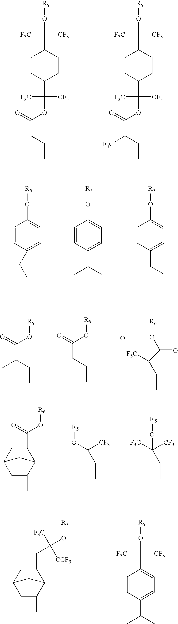
wherein R5 and R6 are conventional acid-sensitive protecting groups as mentioned above, i.e., cyclic or branched aliphatic carbonyls, tertiary esters or tertiary ethers.


or combination of these

Examples of positive-tone silsesquioxane polymers include:


In one embodiment of the present invention the silsesquioxane polymer is a compound having the formula:
wherein R1 and R2 are as defined above; R3 does not equal R1 or R2 and is a group capable of further improving electrical and/or mechanical and/or thermal-mechanical and/or lithograph performance of the polymer; and x, y and z represent the number of repeating units and are integers. y/(x+y+z) is 0.01-1, (x+y)/(x+y+z) is 0.05-1, Preferably, R3 is a sacrificial group capable of further reducing dielectric constant of the resultant low-k composition by generating nanoscopic pores in the polymer resin during curing. R3 is independently alkyl, aryl, cycloalkyl, alkoxy, aryloxy, cycloalkoxy and their fluorinated moieties. Specifically, R3 is linear or branched alkyl, aryl or substituted aryl, cycloalkyl or substituted cycloalkyl, linear or branched alkoxy, aryloxy or substituted aryloxy, cycloalkoxy or substituted cycloalkoxy and their fluorinated moieties comprising 1-40 carbon atoms.


wherein each occurrence of R29 or R30 is preferably independently selected from among H, CH3, C2 or higher alkyl, or halogen. Each occurrence of R31 is preferably independently selected from hydroxyphenyl, cycloalkyl or fluorinated cycloalkyl with a cross-linkable functionality or acid-sensitive protecting group. Each occurrence of R32 is preferably independently selected from among phenyl, hydroxyphenyl, cycloalkyl, fluorinated cycloalkyl, hydroxycyclohexyl, and —COO—R33—OH, wherein R33 may be alkyl, cycloalkyl, aryl or fluorinated alkyl, fluorinated cycloalkyl or fluorinated aryl and R30 may not be halogen when R32 is —COO—R33—OH.


wherein R13 is CH3 or CH2CH3; and R14 and R15 are each independently a C1-C8 alkyl or aryl hydrocarbon;

including their analogs and derivatives, such as those found in Japanese Laid-Open Patent Application (Kokai) No. 1-29339, as well as etherified amino resins, for example methylated or buylated melamine resins (N-methoxymethyl-or N-butoxymethyl-melamine respectively) or methylated/butylated glycolurils, for example as can be found in Canadian Patent No. 1 204 547. Combinations of crosslinking agents may be used.

-
- I. Octakis(dimethylsilyloxy)silsesquioxane(Q8M8 H) (10.16 grams, 0.01 mole), 4-acetoxystyrene(16.22 g, 0.1 mole) and hexane (100 ml) were placed in a round bottom flask equipped with magnetic stirrer, nitrogen inlet, and a water condenser.

Claims (17)


Priority Applications (1)
| Application Number | Priority Date | Filing Date | Title |
|---|---|---|---|
| US11/933,530 US7714079B2 (en) | 2003-01-08 | 2007-11-01 | Patternable low dielectric constant materials and their use in ULSI interconnection |
Applications Claiming Priority (3)
| Application Number | Priority Date | Filing Date | Title |
|---|---|---|---|
| US10/338,945 US7041748B2 (en) | 2003-01-08 | 2003-01-08 | Patternable low dielectric constant materials and their use in ULSI interconnection |
| US11/314,307 US7306853B2 (en) | 2003-01-08 | 2005-12-21 | Patternable low dielectric constant materials and their use in ULSI interconnection |
| US11/933,530 US7714079B2 (en) | 2003-01-08 | 2007-11-01 | Patternable low dielectric constant materials and their use in ULSI interconnection |
Related Parent Applications (1)
| Application Number | Title | Priority Date | Filing Date |
|---|---|---|---|
| US11/314,307 Division US7306853B2 (en) | 2003-01-08 | 2005-12-21 | Patternable low dielectric constant materials and their use in ULSI interconnection |
Publications (2)
| Publication Number | Publication Date |
|---|---|
| US20080063880A1 US20080063880A1 (en) | 2008-03-13 |
| US7714079B2 true US7714079B2 (en) | 2010-05-11 |
Family
ID=32711012
Family Applications (3)
| Application Number | Title | Priority Date | Filing Date |
|---|---|---|---|
| US10/338,945 Expired - Lifetime US7041748B2 (en) | 2003-01-08 | 2003-01-08 | Patternable low dielectric constant materials and their use in ULSI interconnection |
| US11/314,307 Expired - Fee Related US7306853B2 (en) | 2003-01-08 | 2005-12-21 | Patternable low dielectric constant materials and their use in ULSI interconnection |
| US11/933,530 Expired - Fee Related US7714079B2 (en) | 2003-01-08 | 2007-11-01 | Patternable low dielectric constant materials and their use in ULSI interconnection |
Family Applications Before (2)
| Application Number | Title | Priority Date | Filing Date |
|---|---|---|---|
| US10/338,945 Expired - Lifetime US7041748B2 (en) | 2003-01-08 | 2003-01-08 | Patternable low dielectric constant materials and their use in ULSI interconnection |
| US11/314,307 Expired - Fee Related US7306853B2 (en) | 2003-01-08 | 2005-12-21 | Patternable low dielectric constant materials and their use in ULSI interconnection |
Country Status (4)
| Country | Link |
|---|---|
| US (3) | US7041748B2 (en) |
| JP (1) | JP3935874B2 (en) |
| KR (1) | KR100562238B1 (en) |
| TW (1) | TWI320515B (en) |
Cited By (3)
| Publication number | Priority date | Publication date | Assignee | Title |
|---|---|---|---|---|
| US20070254235A1 (en) * | 2006-04-28 | 2007-11-01 | International Business Machines Corporation | Self-topcoating resist for photolithography |
| US8334203B2 (en) | 2010-06-11 | 2012-12-18 | International Business Machines Corporation | Interconnect structure and method of fabricating |
| US9837314B2 (en) * | 2016-02-02 | 2017-12-05 | Tokyo Electron Limited | Self-alignment of metal and via using selective deposition |
Families Citing this family (114)
| Publication number | Priority date | Publication date | Assignee | Title |
|---|---|---|---|---|
| US7261992B2 (en) * | 2000-12-21 | 2007-08-28 | International Business Machines Corporation | Fluorinated silsesquioxane polymers and use thereof in lithographic photoresist compositions |
| TWI288443B (en) | 2002-05-17 | 2007-10-11 | Semiconductor Energy Lab | SiN film, semiconductor device, and the manufacturing method thereof |
| US7507783B2 (en) * | 2003-02-24 | 2009-03-24 | Brewer Science Inc. | Thermally curable middle layer comprising polyhedral oligomeric silsesouioxanes for 193-nm trilayer resist process |
| TWI240959B (en) | 2003-03-04 | 2005-10-01 | Air Prod & Chem | Mechanical enhancement of dense and porous organosilicate materials by UV exposure |
| US7098149B2 (en) * | 2003-03-04 | 2006-08-29 | Air Products And Chemicals, Inc. | Mechanical enhancement of dense and porous organosilicate materials by UV exposure |
| JP4734832B2 (en) * | 2003-05-14 | 2011-07-27 | ナガセケムテックス株式会社 | Encapsulant for optical element |
| WO2005041255A2 (en) * | 2003-08-04 | 2005-05-06 | Honeywell International, Inc. | Coating composition optimization for via fill and photolithography applications and methods of preparation thereof |
| JP5102428B2 (en) * | 2003-11-25 | 2012-12-19 | ローム・アンド・ハース・エレクトロニック・マテリアルズ,エル.エル.シー. | Waveguide composition and waveguide formed therefrom |
| KR100586165B1 (en) * | 2003-12-30 | 2006-06-07 | 동부일렉트로닉스 주식회사 | bottom anti-reflective coating method |
| US7355384B2 (en) * | 2004-04-08 | 2008-04-08 | International Business Machines Corporation | Apparatus, method, and computer program product for monitoring and controlling a microcomputer using a single existing pin |
| US7629272B2 (en) * | 2004-06-07 | 2009-12-08 | Axcelis Technologies, Inc. | Ultraviolet assisted porogen removal and/or curing processes for forming porous low k dielectrics |
| US7563828B2 (en) * | 2004-07-16 | 2009-07-21 | Alcatel-Lucent Usa Inc. | Solid state proton conductor system derived from hybrid composite inorganic-organic multicomponent material |
| JP2006156602A (en) * | 2004-11-26 | 2006-06-15 | Asahi Kasei Corp | Insulating film |
| US7696625B2 (en) | 2004-11-30 | 2010-04-13 | Semiconductor Energy Laboratory Co., Ltd. | Semiconductor device and method for manufacturing the same |
| US7985677B2 (en) * | 2004-11-30 | 2011-07-26 | Semiconductor Energy Laboratory Co., Ltd. | Method of manufacturing semiconductor device |
| US7732349B2 (en) * | 2004-11-30 | 2010-06-08 | Semiconductor Energy Laboratory Co., Ltd. | Manufacturing method of insulating film and semiconductor device |
| US7579224B2 (en) * | 2005-01-21 | 2009-08-25 | Semiconductor Energy Laboratory Co., Ltd. | Method for manufacturing a thin film semiconductor device |
| US7399581B2 (en) * | 2005-02-24 | 2008-07-15 | International Business Machines Corporation | Photoresist topcoat for a photolithographic process |
| US8012673B1 (en) * | 2005-03-01 | 2011-09-06 | Spansion Llc | Processing a copolymer to form a polymer memory cell |
| JP4450214B2 (en) * | 2005-03-11 | 2010-04-14 | セイコーエプソン株式会社 | Organic thin film transistor, electronic device and electronic equipment |
| JP4775561B2 (en) * | 2005-04-01 | 2011-09-21 | 信越化学工業株式会社 | Silsesquioxane-based compound mixture, production method thereof, resist composition using the same, and pattern formation method |
| US7482389B2 (en) | 2005-04-20 | 2009-01-27 | International Business Machines Corporation | Nanoporous media with lamellar structures |
| US7960442B2 (en) * | 2005-04-20 | 2011-06-14 | International Business Machines Corporation | Nanoporous media templated from unsymmetrical amphiphilic porogens |
| US7723438B2 (en) * | 2005-04-28 | 2010-05-25 | International Business Machines Corporation | Surface-decorated polymeric amphiphile porogens for the templation of nanoporous materials |
| US7224050B2 (en) * | 2005-05-25 | 2007-05-29 | Intel Corporation | Plastic materials including dendrimers or hyperbranched polymers for integrated circuit packaging |
| JP4602842B2 (en) * | 2005-06-07 | 2010-12-22 | 東京応化工業株式会社 | Anti-reflection film forming composition and anti-reflection film using the same |
| US7459183B2 (en) * | 2005-07-27 | 2008-12-02 | International Business Machines Corporation | Method of forming low-K interlevel dielectric layers and structures |
| JP4692136B2 (en) * | 2005-08-08 | 2011-06-01 | 東レ株式会社 | Photosensitive paste composition and field emission display member using the same |
| US7449538B2 (en) * | 2005-12-30 | 2008-11-11 | Hynix Semiconductor Inc. | Hard mask composition and method for manufacturing semiconductor device |
| US7468330B2 (en) | 2006-04-05 | 2008-12-23 | International Business Machines Corporation | Imprint process using polyhedral oligomeric silsesquioxane based imprint materials |
| JP2007293159A (en) * | 2006-04-27 | 2007-11-08 | Asahi Kasei Corp | Photosensitive resin composition and silsesquioxane polymer |
| US7704670B2 (en) | 2006-06-22 | 2010-04-27 | Az Electronic Materials Usa Corp. | High silicon-content thin film thermosets |
| JP5074488B2 (en) * | 2006-06-28 | 2012-11-14 | ダウ・コーニング・コーポレイション | Silsesquioxane resin system containing a basic additive with electron withdrawing functionality |
| US8524439B2 (en) * | 2006-06-28 | 2013-09-03 | Dow Corning Corporation | Silsesquioxane resin systems with base additives bearing electron-attracting functionalities |
| US7927664B2 (en) * | 2006-08-28 | 2011-04-19 | International Business Machines Corporation | Method of step-and-flash imprint lithography |
| JP4509080B2 (en) | 2006-09-28 | 2010-07-21 | 信越化学工業株式会社 | Silsesquioxane compound mixture, hydrolyzable silane compound, production method thereof, resist composition using the same, pattern formation method, and substrate processing method |
| US8053375B1 (en) * | 2006-11-03 | 2011-11-08 | Advanced Technology Materials, Inc. | Super-dry reagent compositions for formation of ultra low k films |
| US8026040B2 (en) * | 2007-02-20 | 2011-09-27 | Az Electronic Materials Usa Corp. | Silicone coating composition |
| US7736837B2 (en) * | 2007-02-20 | 2010-06-15 | Az Electronic Materials Usa Corp. | Antireflective coating composition based on silicon polymer |
| KR20090114476A (en) * | 2007-02-26 | 2009-11-03 | 에이제트 일렉트로닉 머트리얼즈 유에스에이 코프. | Process for making siloxane polymers |
| US8524441B2 (en) * | 2007-02-27 | 2013-09-03 | Az Electronic Materials Usa Corp. | Silicon-based antireflective coating compositions |
| JP4963254B2 (en) * | 2007-03-30 | 2012-06-27 | 東京応化工業株式会社 | Film-forming composition for nanoimprint, structure manufacturing method and structure |
| US8084765B2 (en) * | 2007-05-07 | 2011-12-27 | Xerox Corporation | Electronic device having a dielectric layer |
| US7867689B2 (en) * | 2007-05-18 | 2011-01-11 | International Business Machines Corporation | Method of use for photopatternable dielectric materials for BEOL applications |
| US8470516B2 (en) * | 2007-05-18 | 2013-06-25 | International Business Machines Corporation | Method of forming a relief pattern by e-beam lithography using chemical amplification, and derived articles |
| US7709370B2 (en) * | 2007-09-20 | 2010-05-04 | International Business Machines Corporation | Spin-on antireflective coating for integration of patternable dielectric materials and interconnect structures |
| US8618663B2 (en) | 2007-09-20 | 2013-12-31 | International Business Machines Corporation | Patternable dielectric film structure with improved lithography and method of fabricating same |
| US8084862B2 (en) | 2007-09-20 | 2011-12-27 | International Business Machines Corporation | Interconnect structures with patternable low-k dielectrics and method of fabricating same |
| KR100936998B1 (en) * | 2007-10-19 | 2010-01-15 | 에스화인켐 주식회사 | Photosensitive polysilsesquioxane resin composition and method for patterning membranes using the same |
| EP2236543B1 (en) * | 2007-12-10 | 2014-02-26 | Kaneka Corporation | Polysiloxane compound, alkali-developable curable composition, insulating thin film using the same, and thin film transistor |
| US20090174036A1 (en) * | 2008-01-04 | 2009-07-09 | International Business Machines Corporation | Plasma curing of patterning materials for aggressively scaled features |
| US8476758B2 (en) * | 2008-01-09 | 2013-07-02 | International Business Machines Corporation | Airgap-containing interconnect structure with patternable low-k material and method of fabricating |
| US7977256B2 (en) * | 2008-03-06 | 2011-07-12 | Tokyo Electron Limited | Method for removing a pore-generating material from an uncured low-k dielectric film |
| US8029971B2 (en) * | 2008-03-13 | 2011-10-04 | International Business Machines Corporation | Photopatternable dielectric materials for BEOL applications and methods for use |
| WO2010038767A1 (en) | 2008-10-02 | 2010-04-08 | 株式会社カネカ | Photocurable composition and cured product |
| EP2189846B1 (en) * | 2008-11-19 | 2015-04-22 | Rohm and Haas Electronic Materials LLC | Process for photolithography applying a photoresist composition comprising a block copolymer |
| US8227336B2 (en) * | 2009-01-20 | 2012-07-24 | International Business Machines Corporation | Structure with self aligned resist layer on an interconnect surface and method of making same |
| US8168691B2 (en) * | 2009-02-09 | 2012-05-01 | International Business Machines Corporation | Vinyl ether resist formulations for imprint lithography and processes of use |
| KR101715343B1 (en) * | 2009-03-11 | 2017-03-14 | 주식회사 동진쎄미켐 | Method for forming fine pattern in semiconductor device |
| US8728710B2 (en) * | 2009-03-31 | 2014-05-20 | Sam Xunyun Sun | Photo-imageable hardmask with dual tones for microphotolithography |
| US8911932B2 (en) * | 2009-04-13 | 2014-12-16 | Sam Xunyun Sun | Photo-imageable hardmask with positive tone for microphotolithography |
| US8298937B2 (en) * | 2009-06-12 | 2012-10-30 | International Business Machines Corporation | Interconnect structure fabricated without dry plasma etch processing |
| US8519540B2 (en) | 2009-06-16 | 2013-08-27 | International Business Machines Corporation | Self-aligned dual damascene BEOL structures with patternable low- K material and methods of forming same |
| US8659115B2 (en) * | 2009-06-17 | 2014-02-25 | International Business Machines Corporation | Airgap-containing interconnect structure with improved patternable low-K material and method of fabricating |
| US8168109B2 (en) * | 2009-08-21 | 2012-05-01 | International Business Machines Corporation | Stabilizers for vinyl ether resist formulations for imprint lithography |
| US8163658B2 (en) | 2009-08-24 | 2012-04-24 | International Business Machines Corporation | Multiple patterning using improved patternable low-k dielectric materials |
| KR101666097B1 (en) * | 2009-08-27 | 2016-10-13 | 삼성전자 주식회사 | Polyurethane foam composition and polyurethane foam prepared using same |
| JP5381508B2 (en) * | 2009-08-27 | 2014-01-08 | Jsr株式会社 | Negative radiation sensitive composition, cured pattern forming method, and cured pattern |
| US8431670B2 (en) | 2009-08-31 | 2013-04-30 | International Business Machines Corporation | Photo-patternable dielectric materials and formulations and methods of use |
| US8202783B2 (en) | 2009-09-29 | 2012-06-19 | International Business Machines Corporation | Patternable low-k dielectric interconnect structure with a graded cap layer and method of fabrication |
| US8377631B2 (en) | 2009-10-06 | 2013-02-19 | International Business Machines Corporation | Planarization over topography with molecular glass materials |
| US8389663B2 (en) * | 2009-10-08 | 2013-03-05 | International Business Machines Corporation | Photo-patternable dielectric materials curable to porous dielectric materials, formulations, precursors and methods of use thereof |
| US8637395B2 (en) | 2009-11-16 | 2014-01-28 | International Business Machines Corporation | Methods for photo-patternable low-k (PPLK) integration with curing after pattern transfer |
| US8367540B2 (en) | 2009-11-19 | 2013-02-05 | International Business Machines Corporation | Interconnect structure including a modified photoresist as a permanent interconnect dielectric and method of fabricating same |
| US8642252B2 (en) | 2010-03-10 | 2014-02-04 | International Business Machines Corporation | Methods for fabrication of an air gap-containing interconnect structure |
| US8896120B2 (en) | 2010-04-27 | 2014-11-25 | International Business Machines Corporation | Structures and methods for air gap integration |
| US8241992B2 (en) | 2010-05-10 | 2012-08-14 | International Business Machines Corporation | Method for air gap interconnect integration using photo-patternable low k material |
| US8373271B2 (en) | 2010-05-27 | 2013-02-12 | International Business Machines Corporation | Interconnect structure with an oxygen-doped SiC antireflective coating and method of fabrication |
| US8475667B2 (en) | 2010-06-22 | 2013-07-02 | International Business Machines Corporation | Method of patterning photosensitive material on a substrate containing a latent acid generator |
| US8449781B2 (en) | 2010-06-22 | 2013-05-28 | International Business Machines Corporation | Selective etch back process for carbon nanotubes intergration |
| US8853856B2 (en) | 2010-06-22 | 2014-10-07 | International Business Machines Corporation | Methodology for evaluation of electrical characteristics of carbon nanotubes |
| CN101880374B (en) * | 2010-07-09 | 2011-11-30 | 中南民族大学 | Silicon framework hyperbranched epoxy resin and preparation method thereof |
| US8354339B2 (en) | 2010-07-20 | 2013-01-15 | International Business Machines Corporation | Methods to form self-aligned permanent on-chip interconnect structures |
| US8232198B2 (en) | 2010-08-05 | 2012-07-31 | International Business Machines Corporation | Self-aligned permanent on-chip interconnect structure formed by pitch splitting |
| JP2012094726A (en) * | 2010-10-28 | 2012-05-17 | Fujitsu Ltd | Field-effect transistor and method of manufacturing the same |
| US8623447B2 (en) * | 2010-12-01 | 2014-01-07 | Xerox Corporation | Method for coating dielectric composition for fabricating thin-film transistors |
| US8441006B2 (en) * | 2010-12-23 | 2013-05-14 | Intel Corporation | Cyclic carbosilane dielectric films |
| US8617941B2 (en) | 2011-01-16 | 2013-12-31 | International Business Machines Corporation | High-speed graphene transistor and method of fabrication by patternable hard mask materials |
| CN103460135B (en) * | 2011-03-29 | 2017-03-01 | 道康宁公司 | For device fabrication can exposure image and the silsesquioxane resins that can develop |
| US8890318B2 (en) | 2011-04-15 | 2014-11-18 | International Business Machines Corporation | Middle of line structures |
| US8900988B2 (en) | 2011-04-15 | 2014-12-02 | International Business Machines Corporation | Method for forming self-aligned airgap interconnect structures |
| US9054160B2 (en) | 2011-04-15 | 2015-06-09 | International Business Machines Corporation | Interconnect structure and method for fabricating on-chip interconnect structures by image reversal |
| US8822137B2 (en) * | 2011-08-03 | 2014-09-02 | International Business Machines Corporation | Self-aligned fine pitch permanent on-chip interconnect structures and method of fabrication |
| US8614047B2 (en) * | 2011-08-26 | 2013-12-24 | International Business Machines Corporation | Photodecomposable bases and photoresist compositions |
| US20130062732A1 (en) | 2011-09-08 | 2013-03-14 | International Business Machines Corporation | Interconnect structures with functional components and methods for fabrication |
| JP2013149861A (en) * | 2012-01-20 | 2013-08-01 | Sumitomo Chemical Co Ltd | Organic thin-film transistor insulating layer material |
| US8871425B2 (en) * | 2012-02-09 | 2014-10-28 | Az Electronic Materials (Luxembourg) S.A.R.L. | Low dielectric photoimageable compositions and electronic devices made therefrom |
| US9087753B2 (en) | 2012-05-10 | 2015-07-21 | International Business Machines Corporation | Printed transistor and fabrication method |
| EP3528046B1 (en) | 2012-07-04 | 2020-09-09 | Kaneka Corporation | Positive photosensitive composition and thin film transistor |
| JP6086739B2 (en) * | 2013-01-21 | 2017-03-01 | 東京応化工業株式会社 | Insulating film forming composition, insulating film manufacturing method, and insulating film |
| CN103214510B (en) * | 2013-04-10 | 2015-06-24 | 吉林大学 | Octohydroxy cage-like silsesquioxane monomer and preparation method thereof |
| US10351651B2 (en) | 2013-10-30 | 2019-07-16 | Nissan Chemical Industries, Ltd. | Imprint material containing silsesquioxane compound and modified silicone compound |
| JP6323225B2 (en) | 2013-11-01 | 2018-05-16 | セントラル硝子株式会社 | Positive photosensitive resin composition, film production method using the same, and electronic component |
| CN103579102A (en) * | 2013-11-07 | 2014-02-12 | 复旦大学 | Method for preparing low dielectric constant film with excellent mechanical property |
| CN103613611A (en) * | 2013-12-06 | 2014-03-05 | 吉林大学 | Polyhedral oligomeric silsesquioxane with 16-hydroxy and preparation method thereof |
| JP6260579B2 (en) * | 2015-05-01 | 2018-01-17 | 信越化学工業株式会社 | Fluoropolyether group-containing polymer-modified silane, surface treatment agent and article |
| KR102460463B1 (en) * | 2015-06-22 | 2022-10-31 | 인텔 코포레이션 | Image Tone Reversal by Dielectric Using Bottom-Up Crosslinking for Back End of Line (BEOL) Interconnects |
| WO2017056888A1 (en) * | 2015-09-30 | 2017-04-06 | 富士フイルム株式会社 | Pattern formation method, and active-ray-sensitive or radiation-sensitive resin composition |
| CN105254661A (en) * | 2015-10-23 | 2016-01-20 | 航天材料及工艺研究所 | Cage-shaped oligomerization polyhedral silsesquioxane with eight phenolic hydroxyl groups and preparation method thereof |
| CN109415513B (en) * | 2016-06-16 | 2022-02-25 | 美国陶氏有机硅公司 | Silicon-rich silsesquioxane resins |
| KR102242545B1 (en) * | 2017-09-27 | 2021-04-19 | 주식회사 엘지화학 | Antibacterial polymer coating composition and antibacterial polymer film |
| US10573687B2 (en) | 2017-10-31 | 2020-02-25 | International Business Machines Corporation | Magnetic random access memory with permanent photo-patternable low-K dielectric |
| US10950549B2 (en) | 2018-11-16 | 2021-03-16 | International Business Machines Corporation | ILD gap fill for memory device stack array |
| JP2023548814A (en) * | 2020-11-03 | 2023-11-21 | オーティーアイ ルミオニクス インコーポレーテッド | Silicon-containing compounds and devices incorporating the same for forming patterned coatings |
Citations (31)
| Publication number | Priority date | Publication date | Assignee | Title |
|---|---|---|---|---|
| JPS6080851A (en) | 1983-10-11 | 1985-05-08 | Nippon Telegr & Teleph Corp <Ntt> | Pattern forming material and formation of pattern |
| US5290899A (en) | 1988-09-22 | 1994-03-01 | Tosoh Corporation | Photosensitive material having a silicon-containing polymer |
| US5338818A (en) | 1992-09-10 | 1994-08-16 | International Business Machines Corporation | Silicon containing positive resist for DUV lithography |
| US5385804A (en) | 1992-08-20 | 1995-01-31 | International Business Machines Corporation | Silicon containing negative resist for DUV, I-line or E-beam lithography comprising an aromatic azide side group in the polysilsesquioxane polymer |
| US5422223A (en) | 1992-04-30 | 1995-06-06 | International Business Machines Corporation | Silicon-containing positive resist and use in multilayer metal structures |
| US5789460A (en) | 1995-02-02 | 1998-08-04 | Dow Corning Asia, Ltd. | Radiation curable compositions |
| US5820944A (en) | 1996-04-01 | 1998-10-13 | Dow Corning Asia, Ltd. | Ultraviolet-curable composition and method for forming cured-product patterns therefrom |
| US5861235A (en) | 1996-06-26 | 1999-01-19 | Dow Corning Asia, Ltd. | Ultraviolet-curable composition and method for patterning the cured product therefrom |
| US6051625A (en) | 1996-06-27 | 2000-04-18 | Dow Corning Asia, Ltd. | Ultraviolet-curable polysiloxane composition and method for the formation of cured patterns therefrom |
| US6087064A (en) | 1998-09-03 | 2000-07-11 | International Business Machines Corporation | Silsesquioxane polymers, method of synthesis, photoresist composition, and multilayer lithographic method |
| US6096483A (en) | 1996-03-29 | 2000-08-01 | Dow Corning Asia, Ltd. | Radiation-curable composition and method for manufacturing cured-product patterns therefrom |
| US6107357A (en) | 1999-11-16 | 2000-08-22 | International Business Machines Corporatrion | Dielectric compositions and method for their manufacture |
| JP2000281790A (en) | 1999-03-30 | 2000-10-10 | Nippon Steel Chem Co Ltd | Silicon resin and photosensitive resin composition containing same |
| US6187505B1 (en) | 1999-02-02 | 2001-02-13 | International Business Machines Corporation | Radiation sensitive silicon-containing resists |
| US6191183B1 (en) | 1997-02-24 | 2001-02-20 | Dow Corning Toray Silicone Co., Ltd. | Method for the formation of silica thin films |
| US6251486B1 (en) | 1997-09-09 | 2001-06-26 | Agere Systems Guardian Corp. | Method for coating an article with a ladder siloxane polymer and coated article |
| US6271273B1 (en) | 2000-07-14 | 2001-08-07 | Shipley Company, L.L.C. | Porous materials |
| US6342562B1 (en) | 1999-04-23 | 2002-01-29 | Fujitsu Limited | Silicon-containing polymer, process for its production, resist composition employing it, pattern-forming method and electronic device fabrication method |
| US6420084B1 (en) | 2000-06-23 | 2002-07-16 | International Business Machines Corporation | Mask-making using resist having SIO bond-containing polymer |
| US6420088B1 (en) | 2000-06-23 | 2002-07-16 | International Business Machines Corporation | Antireflective silicon-containing compositions as hardmask layer |
| US6420441B1 (en) | 1999-10-01 | 2002-07-16 | Shipley Company, L.L.C. | Porous materials |
| US6472076B1 (en) | 1999-10-18 | 2002-10-29 | Honeywell International Inc. | Deposition of organosilsesquioxane films |
| US6531260B2 (en) | 2000-04-07 | 2003-03-11 | Jsr Corporation | Polysiloxane, method of manufacturing same, silicon-containing alicyclic compound, and radiation-sensitive resin composition |
| US20030073040A1 (en) | 2001-08-24 | 2003-04-17 | Haruo Iwasawa | Pattern forming method and bilayer film |
| US20030099899A1 (en) | 2001-05-08 | 2003-05-29 | Gronbeck Dana A. | Photoimageable composition |
| US6576345B1 (en) | 2000-11-30 | 2003-06-10 | Novellus Systems Inc | Dielectric films with low dielectric constants |
| US6653045B2 (en) | 2001-02-16 | 2003-11-25 | International Business Machines Corporation | Radiation sensitive silicon-containing negative resists and use thereof |
| US6762501B1 (en) | 2003-04-14 | 2004-07-13 | Texas Instruments Incorporated | Low stress integrated circuit copper interconnect structures |
| US20040138355A1 (en) * | 2001-01-24 | 2004-07-15 | Hideo Saito | Polyphentlene ether resin composition containing silicon compounds |
| US6774031B2 (en) * | 2002-12-17 | 2004-08-10 | Texas Instruments Incorporated | Method of forming dual-damascene structure |
| US6873026B1 (en) | 2002-03-04 | 2005-03-29 | Novellus Systems, Inc. | Inhomogeneous materials having physical properties decoupled from desired functions |
Family Cites Families (1)
| Publication number | Priority date | Publication date | Assignee | Title |
|---|---|---|---|---|
| JP2000501070A (en) * | 1995-09-28 | 2000-02-02 | メルク シヤープ エンド ドーム リミテツド | Substituted indolylpropylpiperazine derivatives as 5-HT 1Dα agonists |
-
2003
- 2003-01-08 US US10/338,945 patent/US7041748B2/en not_active Expired - Lifetime
- 2003-12-08 KR KR1020030088568A patent/KR100562238B1/en not_active IP Right Cessation
- 2003-12-18 JP JP2003421691A patent/JP3935874B2/en not_active Expired - Lifetime
-
2004
- 2004-01-05 TW TW93100144A patent/TWI320515B/en not_active IP Right Cessation
-
2005
- 2005-12-21 US US11/314,307 patent/US7306853B2/en not_active Expired - Fee Related
-
2007
- 2007-11-01 US US11/933,530 patent/US7714079B2/en not_active Expired - Fee Related
Patent Citations (35)
| Publication number | Priority date | Publication date | Assignee | Title |
|---|---|---|---|---|
| JPS6080851A (en) | 1983-10-11 | 1985-05-08 | Nippon Telegr & Teleph Corp <Ntt> | Pattern forming material and formation of pattern |
| US5290899A (en) | 1988-09-22 | 1994-03-01 | Tosoh Corporation | Photosensitive material having a silicon-containing polymer |
| US5422223A (en) | 1992-04-30 | 1995-06-06 | International Business Machines Corporation | Silicon-containing positive resist and use in multilayer metal structures |
| US5385804A (en) | 1992-08-20 | 1995-01-31 | International Business Machines Corporation | Silicon containing negative resist for DUV, I-line or E-beam lithography comprising an aromatic azide side group in the polysilsesquioxane polymer |
| US5338818A (en) | 1992-09-10 | 1994-08-16 | International Business Machines Corporation | Silicon containing positive resist for DUV lithography |
| US5891529A (en) | 1995-02-02 | 1999-04-06 | Dow Corning Asia, Ltd. | Radiation curable sompositions |
| US5789460A (en) | 1995-02-02 | 1998-08-04 | Dow Corning Asia, Ltd. | Radiation curable compositions |
| US6096483A (en) | 1996-03-29 | 2000-08-01 | Dow Corning Asia, Ltd. | Radiation-curable composition and method for manufacturing cured-product patterns therefrom |
| US5820944A (en) | 1996-04-01 | 1998-10-13 | Dow Corning Asia, Ltd. | Ultraviolet-curable composition and method for forming cured-product patterns therefrom |
| US5861235A (en) | 1996-06-26 | 1999-01-19 | Dow Corning Asia, Ltd. | Ultraviolet-curable composition and method for patterning the cured product therefrom |
| US6051625A (en) | 1996-06-27 | 2000-04-18 | Dow Corning Asia, Ltd. | Ultraviolet-curable polysiloxane composition and method for the formation of cured patterns therefrom |
| US6258506B1 (en) | 1996-06-27 | 2001-07-10 | Dow Corning Asia, Ltd. | Ultraviolet-curable polysiloxane composition and method for the formation of cured patterns therefrom |
| US6191183B1 (en) | 1997-02-24 | 2001-02-20 | Dow Corning Toray Silicone Co., Ltd. | Method for the formation of silica thin films |
| US6251486B1 (en) | 1997-09-09 | 2001-06-26 | Agere Systems Guardian Corp. | Method for coating an article with a ladder siloxane polymer and coated article |
| US6087064A (en) | 1998-09-03 | 2000-07-11 | International Business Machines Corporation | Silsesquioxane polymers, method of synthesis, photoresist composition, and multilayer lithographic method |
| US6340734B1 (en) | 1998-09-03 | 2002-01-22 | International Business Machines Corporation | Silsesquioxane polymers, method of synthesis, photoresist composition, and multilayer lithographic method |
| US6187505B1 (en) | 1999-02-02 | 2001-02-13 | International Business Machines Corporation | Radiation sensitive silicon-containing resists |
| JP2000281790A (en) | 1999-03-30 | 2000-10-10 | Nippon Steel Chem Co Ltd | Silicon resin and photosensitive resin composition containing same |
| US6767983B1 (en) | 1999-03-30 | 2004-07-27 | Nippon Steel Chemical Co., Ltd. | Silicone resin and photosensitive resin composition containing the same |
| US6342562B1 (en) | 1999-04-23 | 2002-01-29 | Fujitsu Limited | Silicon-containing polymer, process for its production, resist composition employing it, pattern-forming method and electronic device fabrication method |
| US6420441B1 (en) | 1999-10-01 | 2002-07-16 | Shipley Company, L.L.C. | Porous materials |
| US6472076B1 (en) | 1999-10-18 | 2002-10-29 | Honeywell International Inc. | Deposition of organosilsesquioxane films |
| US6107357A (en) | 1999-11-16 | 2000-08-22 | International Business Machines Corporatrion | Dielectric compositions and method for their manufacture |
| US6531260B2 (en) | 2000-04-07 | 2003-03-11 | Jsr Corporation | Polysiloxane, method of manufacturing same, silicon-containing alicyclic compound, and radiation-sensitive resin composition |
| US6420088B1 (en) | 2000-06-23 | 2002-07-16 | International Business Machines Corporation | Antireflective silicon-containing compositions as hardmask layer |
| US6420084B1 (en) | 2000-06-23 | 2002-07-16 | International Business Machines Corporation | Mask-making using resist having SIO bond-containing polymer |
| US6271273B1 (en) | 2000-07-14 | 2001-08-07 | Shipley Company, L.L.C. | Porous materials |
| US6576345B1 (en) | 2000-11-30 | 2003-06-10 | Novellus Systems Inc | Dielectric films with low dielectric constants |
| US20040138355A1 (en) * | 2001-01-24 | 2004-07-15 | Hideo Saito | Polyphentlene ether resin composition containing silicon compounds |
| US6653045B2 (en) | 2001-02-16 | 2003-11-25 | International Business Machines Corporation | Radiation sensitive silicon-containing negative resists and use thereof |
| US20030099899A1 (en) | 2001-05-08 | 2003-05-29 | Gronbeck Dana A. | Photoimageable composition |
| US20030073040A1 (en) | 2001-08-24 | 2003-04-17 | Haruo Iwasawa | Pattern forming method and bilayer film |
| US6873026B1 (en) | 2002-03-04 | 2005-03-29 | Novellus Systems, Inc. | Inhomogeneous materials having physical properties decoupled from desired functions |
| US6774031B2 (en) * | 2002-12-17 | 2004-08-10 | Texas Instruments Incorporated | Method of forming dual-damascene structure |
| US6762501B1 (en) | 2003-04-14 | 2004-07-13 | Texas Instruments Incorporated | Low stress integrated circuit copper interconnect structures |
Non-Patent Citations (2)
| Title |
|---|
| "Silsesquioxanes as models for silica surfaces", J. Amer. Chem. Soc., 1989, 111 (5), 1741-1748, to Frank J. Feher, David A. Newman and John F. Walzer. * |
| Harkness, et al., "Demonstration of a Directly Photopatternable Spin-On-Glass Based on Hydrogen Silsesquioxane and Photobase Generators", Macromolecules, American Chemical Society, 1998, 31, pp. 4798-4805. |
Cited By (5)
| Publication number | Priority date | Publication date | Assignee | Title |
|---|---|---|---|---|
| US20070254235A1 (en) * | 2006-04-28 | 2007-11-01 | International Business Machines Corporation | Self-topcoating resist for photolithography |
| US8945808B2 (en) * | 2006-04-28 | 2015-02-03 | International Business Machines Corporation | Self-topcoating resist for photolithography |
| US8334203B2 (en) | 2010-06-11 | 2012-12-18 | International Business Machines Corporation | Interconnect structure and method of fabricating |
| US8916978B2 (en) | 2010-06-11 | 2014-12-23 | International Business Machines Corporation | Interconnect structure and method of fabricating |
| US9837314B2 (en) * | 2016-02-02 | 2017-12-05 | Tokyo Electron Limited | Self-alignment of metal and via using selective deposition |
Also Published As
| Publication number | Publication date |
|---|---|
| KR100562238B1 (en) | 2006-03-22 |
| US7041748B2 (en) | 2006-05-09 |
| US20080063880A1 (en) | 2008-03-13 |
| JP3935874B2 (en) | 2007-06-27 |
| TWI320515B (en) | 2010-02-11 |
| TW200508803A (en) | 2005-03-01 |
| US20060105181A1 (en) | 2006-05-18 |
| KR20040063769A (en) | 2004-07-14 |
| US7306853B2 (en) | 2007-12-11 |
| US20040137241A1 (en) | 2004-07-15 |
| JP2004212983A (en) | 2004-07-29 |
Similar Documents
| Publication | Publication Date | Title |
|---|---|---|
| US7714079B2 (en) | Patternable low dielectric constant materials and their use in ULSI interconnection | |
| US7709370B2 (en) | Spin-on antireflective coating for integration of patternable dielectric materials and interconnect structures | |
| US7172849B2 (en) | Antireflective hardmask and uses thereof | |
| US7666794B2 (en) | Multiple patterning using patternable low-k dielectric materials | |
| JP5285814B2 (en) | Patternable low-k dielectric wiring structure with stepped cap layer, air gap inclusion wiring structure, and fabrication method | |
| US7867689B2 (en) | Method of use for photopatternable dielectric materials for BEOL applications | |
| US7919225B2 (en) | Photopatternable dielectric materials for BEOL applications and methods for use | |
| US8946371B2 (en) | Photo-patternable dielectric materials curable to porous dielectric materials, formulations, precursors and methods of use thereof | |
| US8659115B2 (en) | Airgap-containing interconnect structure with improved patternable low-K material and method of fabricating | |
| US20140131880A1 (en) | Methods for fabrication of an air gap-containing interconnect structure | |
| US8487411B2 (en) | Multiple patterning using improved patternable low-κ dielectric materials | |
| US8232198B2 (en) | Self-aligned permanent on-chip interconnect structure formed by pitch splitting | |
| US8431670B2 (en) | Photo-patternable dielectric materials and formulations and methods of use | |
| US20110115090A1 (en) | Interconnect structure including a modified photoresist as a permanent interconnect dielectric and method of fabricating same |
Legal Events
| Date | Code | Title | Description |
|---|---|---|---|
| FEPP | Fee payment procedure |
Free format text: PAYOR NUMBER ASSIGNED (ORIGINAL EVENT CODE: ASPN); ENTITY STATUS OF PATENT OWNER: LARGE ENTITY |
|
| STCF | Information on status: patent grant |
Free format text: PATENTED CASE |
|
| REMI | Maintenance fee reminder mailed | ||
| FPAY | Fee payment |
Year of fee payment: 4 |
|
| SULP | Surcharge for late payment | ||
| AS | Assignment |
Owner name: GLOBALFOUNDRIES U.S. 2 LLC, NEW YORK Free format text: ASSIGNMENT OF ASSIGNORS INTEREST;ASSIGNOR:INTERNATIONAL BUSINESS MACHINES CORPORATION;REEL/FRAME:036550/0001 Effective date: 20150629 |
|
| AS | Assignment |
Owner name: GLOBALFOUNDRIES INC., CAYMAN ISLANDS Free format text: ASSIGNMENT OF ASSIGNORS INTEREST;ASSIGNORS:GLOBALFOUNDRIES U.S. 2 LLC;GLOBALFOUNDRIES U.S. INC.;REEL/FRAME:036779/0001 Effective date: 20150910 |
|
| AS | Assignment |
Owner name: AURIGA INNOVATIONS, INC., CANADA Free format text: ASSIGNMENT OF ASSIGNORS INTEREST;ASSIGNOR:GLOBALFOUNDRIES INC.;REEL/FRAME:041741/0358 Effective date: 20161207 |
|
| MAFP | Maintenance fee payment |
Free format text: PAYMENT OF MAINTENANCE FEE, 8TH YEAR, LARGE ENTITY (ORIGINAL EVENT CODE: M1552) Year of fee payment: 8 |
|
| FEPP | Fee payment procedure |
Free format text: MAINTENANCE FEE REMINDER MAILED (ORIGINAL EVENT CODE: REM.); ENTITY STATUS OF PATENT OWNER: LARGE ENTITY |
|
| LAPS | Lapse for failure to pay maintenance fees |
Free format text: PATENT EXPIRED FOR FAILURE TO PAY MAINTENANCE FEES (ORIGINAL EVENT CODE: EXP.); ENTITY STATUS OF PATENT OWNER: LARGE ENTITY |
|
| STCH | Information on status: patent discontinuation |
Free format text: PATENT EXPIRED DUE TO NONPAYMENT OF MAINTENANCE FEES UNDER 37 CFR 1.362 |
|
| FP | Lapsed due to failure to pay maintenance fee |
Effective date: 20220511 |