US7710476B2 - Color filter array, imaging device, and image processing unit - Google Patents
Color filter array, imaging device, and image processing unit Download PDFInfo
- Publication number
- US7710476B2 US7710476B2 US11/714,261 US71426107A US7710476B2 US 7710476 B2 US7710476 B2 US 7710476B2 US 71426107 A US71426107 A US 71426107A US 7710476 B2 US7710476 B2 US 7710476B2
- Authority
- US
- United States
- Prior art keywords
- color
- filters
- pixel
- present
- pixels
- Prior art date
- Legal status (The legal status is an assumption and is not a legal conclusion. Google has not performed a legal analysis and makes no representation as to the accuracy of the status listed.)
- Expired - Fee Related, expires
Links
- 238000012545 processing Methods 0.000 title claims description 71
- 238000003384 imaging method Methods 0.000 title claims description 32
- 230000035945 sensitivity Effects 0.000 claims abstract description 32
- 230000003595 spectral effect Effects 0.000 claims abstract description 31
- 239000003086 colorant Substances 0.000 claims description 74
- 230000001131 transforming effect Effects 0.000 claims 4
- 238000000034 method Methods 0.000 description 108
- 230000008569 process Effects 0.000 description 67
- 230000000875 corresponding effect Effects 0.000 description 14
- 238000012937 correction Methods 0.000 description 13
- 238000010586 diagram Methods 0.000 description 13
- 230000015654 memory Effects 0.000 description 8
- 230000004048 modification Effects 0.000 description 8
- 238000012986 modification Methods 0.000 description 8
- 238000005070 sampling Methods 0.000 description 8
- 230000003287 optical effect Effects 0.000 description 7
- 238000000926 separation method Methods 0.000 description 7
- 230000007423 decrease Effects 0.000 description 6
- 230000003247 decreasing effect Effects 0.000 description 3
- 239000000284 extract Substances 0.000 description 3
- 230000009467 reduction Effects 0.000 description 3
- 238000012935 Averaging Methods 0.000 description 2
- 230000008901 benefit Effects 0.000 description 2
- 230000002596 correlated effect Effects 0.000 description 2
- 230000006870 function Effects 0.000 description 2
- 238000012417 linear regression Methods 0.000 description 2
- 230000004075 alteration Effects 0.000 description 1
- 238000006243 chemical reaction Methods 0.000 description 1
- 238000013461 design Methods 0.000 description 1
- 238000009434 installation Methods 0.000 description 1
- 230000004044 response Effects 0.000 description 1
- 239000004065 semiconductor Substances 0.000 description 1
- 238000002834 transmittance Methods 0.000 description 1
Images


Classifications
-
- F—MECHANICAL ENGINEERING; LIGHTING; HEATING; WEAPONS; BLASTING
- F21—LIGHTING
- F21V—FUNCTIONAL FEATURES OR DETAILS OF LIGHTING DEVICES OR SYSTEMS THEREOF; STRUCTURAL COMBINATIONS OF LIGHTING DEVICES WITH OTHER ARTICLES, NOT OTHERWISE PROVIDED FOR
- F21V9/00—Elements for modifying spectral properties, polarisation or intensity of the light emitted, e.g. filters
- F21V9/08—Elements for modifying spectral properties, polarisation or intensity of the light emitted, e.g. filters for producing coloured light, e.g. monochromatic; for reducing intensity of light
-
- H—ELECTRICITY
- H04—ELECTRIC COMMUNICATION TECHNIQUE
- H04N—PICTORIAL COMMUNICATION, e.g. TELEVISION
- H04N25/00—Circuitry of solid-state image sensors [SSIS]; Control thereof
- H04N25/10—Circuitry of solid-state image sensors [SSIS]; Control thereof for transforming different wavelengths into image signals
- H04N25/11—Arrangement of colour filter arrays [CFA]; Filter mosaics
- H04N25/13—Arrangement of colour filter arrays [CFA]; Filter mosaics characterised by the spectral characteristics of the filter elements
- H04N25/135—Arrangement of colour filter arrays [CFA]; Filter mosaics characterised by the spectral characteristics of the filter elements based on four or more different wavelength filter elements
-
- H—ELECTRICITY
- H01—ELECTRIC ELEMENTS
- H01L—SEMICONDUCTOR DEVICES NOT COVERED BY CLASS H10
- H01L27/00—Devices consisting of a plurality of semiconductor or other solid-state components formed in or on a common substrate
- H01L27/14—Devices consisting of a plurality of semiconductor or other solid-state components formed in or on a common substrate including semiconductor components sensitive to infrared radiation, light, electromagnetic radiation of shorter wavelength or corpuscular radiation and specially adapted either for the conversion of the energy of such radiation into electrical energy or for the control of electrical energy by such radiation
- H01L27/144—Devices controlled by radiation
- H01L27/146—Imager structures
-
- H—ELECTRICITY
- H04—ELECTRIC COMMUNICATION TECHNIQUE
- H04N—PICTORIAL COMMUNICATION, e.g. TELEVISION
- H04N23/00—Cameras or camera modules comprising electronic image sensors; Control thereof
- H04N23/80—Camera processing pipelines; Components thereof
- H04N23/84—Camera processing pipelines; Components thereof for processing colour signals
- H04N23/843—Demosaicing, e.g. interpolating colour pixel values
-
- H—ELECTRICITY
- H04—ELECTRIC COMMUNICATION TECHNIQUE
- H04N—PICTORIAL COMMUNICATION, e.g. TELEVISION
- H04N25/00—Circuitry of solid-state image sensors [SSIS]; Control thereof
- H04N25/10—Circuitry of solid-state image sensors [SSIS]; Control thereof for transforming different wavelengths into image signals
- H04N25/11—Arrangement of colour filter arrays [CFA]; Filter mosaics
- H04N25/13—Arrangement of colour filter arrays [CFA]; Filter mosaics characterised by the spectral characteristics of the filter elements
- H04N25/134—Arrangement of colour filter arrays [CFA]; Filter mosaics characterised by the spectral characteristics of the filter elements based on three different wavelength filter elements
Definitions
- the present invention contains subject matter related to Japanese Patent Application JP 2006-069541 filed in the Japanese Patent Office on Mar. 14, 2006, the entire contents of which are incorporated herein by reference.
- the present invention relates to a color filter array, an imaging device, and an image processing unit used for an image capturing apparatus, such as a digital camera using a solid-state imaging device.
- Single-plate color image capturing apparatuses that include an image processing unit are known.
- a color filter is bonded to each of a plurality of pixels of a single-plate solid-state imaging device and the image processing unit allocates all colors to the position of each pixel using a mosaic image of colors captured by the imaging device.
- a Bayer array format described in Bryce E. Bayer, U.S. Pat. No. 3,971,065 entitled “COLOR IMAGING ARRAY” is used as a color filter arrangement.
- G color filters are arranged in a checkered pattern so that the density of the G color filters is twice that of R color filters or B color filters. Accordingly, in most methods of interpolating a color of a pixel, a G color having a large amount of information and a strong relation to the brightness of light is interpolated to all the pixels first, and subsequently, R and B colors are interpolated using the G color as a reference.
- Japanese Patent No. 2931520 entitled “Color Separation Circuit of Single-plate Color Video Camera” describes a technique in which a correlation value at the position of an interpolated pixel in a horizontal direction or in a vertical direction is computed. Two interpolation values obtained by processing means appropriate when the correlation in the horizontal direction is strong and processing means appropriate when the correlation in the vertical direction is strong are mixed using the correlation value.
- the R, G, and B colors can be allocated to positions of all the pixels for high-resolution display.
- This color is referred to as a “false color”.
- the false color is noticeable when a color filter arrangement in which color filters are regularly arranged is used, since a significant overlap occurs in a specific spatial frequency range. Once a false color is generated, it cannot be determined whether a color is an original color having an original low frequency or the false color caused by the overlap of a high-frequency component. Therefore, the false color cannot be removed by using a frequency filter.
- known single-plate color image capturing apparatuses need to include an optical low-pass filter disposed in front of the imaging device so as to remove a high-frequency component in advance.
- the optical low-pass filter does not have a sharp cut-off capability for the Nyquist frequency. Therefore, if the single-plate color image capturing apparatuses attempt to completely prevent the occurrence of the false color, low-frequency components having a frequency lower than the Nyquist frequency could also be cut off.
- the Nyquist frequency of the R signal or the B signal is lower than that of the G signal. Accordingly, an optical low-pass filter suitable for the Nyquist frequency of the R channel or the B channel decreases the resolution of the G channel.
- the fidelity and the dynamic range of colors can be increased by using a filter arrangement of four colors or more.
- a method using a large number of filters each transmitting light only in a narrow wavelength range is more suitable than a method using a small number of filters each transmitting light in a wide wavelength range, as shown in FIG. 2C .
- a method using a plurality of filters that have different transmittances but transmit light in the same wavelength range is more suitable than a method using the filters shown in FIG. 2C .
- this technology solves the following problem. That is, a false color is visually noticeable and removal of the false color is difficult if most of the false colors occur in a specific spatial frequency range.
- the reduction in the occurrence of a false color refers to the reduction in the occurrence of a false color concentrated in a specific spatial frequency range.
- G color filters are arranged in a checkered pattern.
- R and B color filters are pseudo-randomly arranged. This arrangement is referred to as a “three-color G-checkered pseudo-random arrangement”.
- Japanese Unexamined Patent Application Publication No. 2000-316169 describes a six-color random arrangement in which four sides or four corners of a pixel of interest are adjacent to filters of six colors.
- Mutze, Ulrich, Dr., EP Patent Publication No. 0,804,037 entitled “Process and system for generating a full color image or multispectral image from the image data of a CCD image sensor with a mosaic color filter” describes an arrangement including a five-color 3-by-3 repetition pattern and a pseudo-random pattern.
- the false color is dispersed in a variety of spatial frequency ranges, and therefore, the false color is not noticeable.
- the increase in the number of filters improves the dynamic range and the performance of the color reproduction.
- the pseudo-random Bayer arrangement introduced by FillFactory has a pseudo-random pattern, only the positions at which a false color occurs in the spatial frequency range are slightly different from those in the Bayer arrangement. This is because the frequency of the repetition is low. Therefore, in practice, the pseudo-random Bayer arrangement reduces the occurrence of a false color little.
- the pseudo-random Bayer arrangement is a three-color filter arrangement, the performance of color reproduction and the dynamic range are substantially the same as those of the Bayer arrangement.
- one color signal is interpolated with a high resolution first. Thereafter, the other color signals are interpolated using that color signal as a reference. Accordingly, compared with the Bayer arrangement or the pseudo-random Bayer arrangement in which G color filters are arranged in a checkered pattern and a correlation process described in Japanese Patent No. 2931520 is used, it is very difficult for the arrangements described in Japanese Unexamined Patent Application Publication No. 2000-316169 and EP Patent Publication No. 0,804,037, (A2) to generate a reference color. Consequently, the reproducible frequency range is significantly different for the position of each pixel.
- the signals from the pixels are thinned out (dumped) or summed.
- the dumping and summing processes are cyclically executed. Accordingly, if a random filter arrangement is used, a filter pattern after dumping may be changed from the original pattern or signals from different pixels may be summed.
- the random pattern and the increase in the number of colors decrease the resolution and cause an unsuccessful operation of dumping and summing the signals from the pixels.
- the present invention provides a color filter array, an imaging device, and an image processing unit capable of sufficiently preventing a decrease in resolution and the occurrence of a false color and supporting dumping and summing processes of signals from pixels even when filters of colors more than that of the Bayer arrangement are used.
- a color filter array includes a plurality of filters, each having one of a plurality of types of spectral sensitivity and being disposed at the location of a corresponding one of a plurality of pixels.
- the filters of a predetermined type selected from among the plurality of types are arranged at the locations of the pixels in a checkered pattern, and the filters of some or all of the other types are randomly arranged at the pixel locations at which the filters of the predetermined type are not present.
- a color filter array includes a plurality of filters, each having one of at least five types of spectral sensitivity and being disposed at the location of a corresponding one of a plurality of pixels.
- the filters of a first color C 1 a selected from among the at least five types of color are arranged at the locations of the pixels on every other line in a horizontal direction and a vertical direction
- the filters of a second color C 1 b selected from among the at least five types of color are arranged at the pixel locations at which the filters of the first color C 1 a are not present on every other line in a horizontal direction and a vertical direction
- the filters of some or all of the other colors are randomly arranged at the pixel locations at which neither the filters of the first color C 1 a nor the second color C 1 b are present.
- an imaging device includes a color filter array including a plurality of filters, each having one of a plurality of types of spectral sensitivity and being disposed at the location of a corresponding one of a plurality of pixels.
- the filters of a predetermined type selected from among the plurality of types are arranged at the locations of the pixels in a checkered pattern, and the filters of some or all of the other types are randomly arranged at the pixel locations at which the filters of the predetermined type are not present.
- an imaging device includes a color filter array including a plurality of filters, each having one of at least five types of spectral sensitivity and being disposed at the location of a corresponding one of a plurality of pixels.
- the filters of a first color C 1 a selected from among the at least five types of color are arranged at the locations of the pixels on every other line in a horizontal direction and a vertical direction
- the filters of a second color C 1 b selected from among the at least five types of color are arranged at the pixel locations at which the filters of the first color C 1 a are not present on every other line in a horizontal direction and a vertical direction
- the filters of some or all of the other colors are randomly arranged at the pixel locations at which neither the filters of the first color C 1 a nor the second color C 1 b are present.
- an image processing unit includes receiving means for receiving image data from an imaging device including a color filter array, first interpolating means, and second interpolating means.
- the color filter array includes a plurality of filters, each having one of a plurality of types of spectral sensitivity and being disposed at the location of a corresponding one of a plurality of pixels.
- the filters of a predetermined type selected from among the plurality of types are arranged at the locations of the pixels in a checkered pattern, and the filters of some or all of the other types are randomly arranged at the pixel locations at which the filters of the predetermined type are not present.
- the first interpolating means interpolates a pixel value of a first color C 1 at a pixel location of the image data received by the receiving means at which the predetermined color is not present using the colors C 1 present in the vicinity of the pixel location so as to generate a first image.
- the second interpolating means interpolates a pixel value of a second color CX different from the first color C 1 using the first colors C 1 and the second colors CX that are present in a local region including a pixel of interest so as to generate a second image.
- an image processing unit includes receiving means for receiving image data from an imaging device including a color filter array, first interpolating means, and second interpolating means.
- the color filter array includes a plurality of filters, each having one of at least five types of spectral sensitivity and being disposed at the location of a corresponding one of a plurality of pixels.
- the filters of a first color C 1 a selected from among the at least five types of color are arranged at the locations of the pixels on every other line in a horizontal direction and a vertical direction
- the filters of a second color C 1 b selected from among the at least five types of color are arranged at the pixel locations at which the filters of the first color C 1 a are not present on every other line in a horizontal direction and a vertical direction
- the filters of some or all of the other colors are randomly arranged at the pixel locations at which neither the filters of the first color C 1 a nor the second color C 1 b are present.
- the first interpolating means interpolate a pixel value of a third color C 1 c at a pixel location of a pixel of interest using the pixel values of the first color C 1 a and the second color C 1 b that are present in a local region including the pixel of interest in the image data received by the receiving means.
- the second interpolating means interpolates a pixel value of each color CX of the plurality of filter colors including the color C 1 a and the color C 1 b by using the pixel values of the third color C 1 c and the color CX that are present in the local region including the pixel of interest.
- a color filter array, an imaging device, and an image processing unit capable of sufficiently preventing a decrease in resolution and the occurrence of a false color and supporting dumping and summing processes of signals from a plurality of pixels even when filters of colors more than that of the Bayer arrangement are used.
- FIG. 1 is a diagram illustrating the structure of known color filter array
- FIGS. 2A-2C illustrate the characteristics of examples of a color filter array
- FIG. 3 is a diagram illustrating the structure of a color filter array according to a first exemplary embodiment of the present invention
- FIG. 4 is a diagram illustrating a modification of a color filter array according to the first exemplary embodiment of the present invention
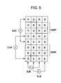
- FIG. 5 illustrates an example in which signals are read out from a solid-state imaging device using a combination of the dumping readout technique and the summing readout technique
- FIG. 6 is a diagram in which pixels that are present in a local space are plotted in a G-B plane
- FIG. 7 is a diagram illustrating the structure of a color filter array having a five-color G checkered random arrangement according to the first exemplary embodiment of the present invention.
- FIG. 8 is a block diagram of an exemplary structure of a digital video camera according to an embodiment of the present invention.
- FIG. 9 is a block diagram of processing of an image processing unit shown in FIG. 8 according to the embodiment of the present invention.
- FIG. 10 is a flow chart of a process performed by a G interpolation unit shown in FIG. 9 ;
- FIG. 11 is a flow chart of a process performed by an R interpolation unit shown in FIG. 9 ;
- FIGS. 12A and 12B are flow charts of processes performed at step ST 404 and ST 405 shown in FIG. 11 , respectively;
- FIG. 13 is a block diagram of a detailed structure of an R MS-SyncNR unit 207 shown in FIG. 9 ;
- FIG. 14 is a block diagram illustrating an exemplary configuration of a correction unit
- FIG. 15 illustrates an exemplary structure of a color filter array according to a second exemplary embodiment of the present invention
- FIG. 16 illustrates a demosaic process performed when the color filter array shown in FIG. 15 is used
- FIG. 17 illustrates a modification of the color filter array according to the second exemplary embodiment of the present invention.
- a color filter array, an imaging device, and an image processing unit according to exemplary embodiments of the present invention are now herein described.
- a filter arrangement is used for an imaging device in which one of a plurality of filters having different color separation characteristics (i.e., colors) is bonded to each pixel.
- the filter arrangement includes four colors or more.
- a color C 1 is arranged in a checkered pattern. Some or all of the other colors are randomly arranged at pixel locations at which the color C 1 is not present.
- color refers to a filter or a pixel value of that color obtained from the filter.
- the color C 1 has a checkered pattern
- a correlation process that is applied to a G-color checkered pattern of the Bayer arrangement can be applied to the C 1 checkered pattern. Accordingly, a signal in a high-frequency range can be reproduced.
- the color CX that is finally obtained at every position of the pixel can be reproduced as a signal containing the high-frequency component.
- FIG. 3 An exemplary color filter arrangement according to the present exemplary embodiment is shown in FIG. 3 .
- This color filter arrangement is a five-color arrangement in which the color filters C 1 are arranged in a checkered pattern and color filters C 2 , C 3 , C 4 , and C 5 are randomly arranged at positions at which the color filters C 1 are not present.
- the occurrence frequency of a color in an area including the pixel of interest and having a predetermined size is within a desired error range.
- the color needs to be present in the vicinity of the pixel of interest.
- the occurrence frequency of a color in a local region needs to be within a desired range so as to avoid a filter arrangement in which only a specific color dominates.
- An arrangement that satisfies the above-described conditions may be obtained through a plurality of attempts of random arrangements.
- a digital halftone technology in which colors are equally randomly distributed in a local region may be applied.
- randomly does not necessarily mean “completely randomly”, but may mean “pseudo-randomly”. That is, repetition may occur over a long cycle.
- the occurrence frequency of a color in the end portions (the upper, lower, left, and light portions) of the filter arrangement may be computed while taking into account a space in which the upper end is connected to the lower end of the arrangement and the left end is connected to the right end of the arrangement.
- the end portions may be negligible if the filter arrangement is sufficiently large compared with a predetermined area size.
- the color filter arrangement shown in FIG. 3 is a five-color filter arrangement in which the color filters C 1 are arranged in a checkered pattern and the color filters C 2 , C 3 , C 4 , and C 5 are randomly arranged at positions at which the color filters C 1 are not present.
- the area having a predetermined size is a rectangle of 15 by 15 pixels.
- the occurrence frequency of the color filters C 1 is determined as a ratio of 1/2 whereas the occurrence frequency of each of the color filters C 2 , C 3 , C 4 , and C 5 are determined as a ratio of 1/8.
- the error of the occurrence frequency is determined to be ⁇ 1/50.
- a color filter arrangement is a four-color filter arrangement in which first color filters C 1 are arranged in a checkered pattern, second color filters C 2 are arranged at positions at which the color filters C 1 are not present on every other line in a horizontal direction and in a vertical direction, and third color filters C 3 and fourth color filters C 4 are randomly arranged at positions at which neither the color filters C 1 nor C 2 are present.
- the color filters C 1 and C 2 are regularly arranged whereas the color filters C 3 and C 4 are randomly arranged.
- the color filters C 1 correspond to a number of pixels about half the total number of pixels of the imaging device.
- the color filters C 2 correspond to a number of pixels about one fourth of the total number of pixels of the imaging device.
- the color filters C 3 and C 4 totally correspond to a number of pixels only one fourth of the total number of pixels of the imaging device. Accordingly, when the numbers of pixels having the color filters C 3 is substantially the same as the number of pixels having the color filters C 4 , the number of the color filters C 3 or C 4 is about one eighth of the total number of pixels of the imaging device. Therefore, the resolution is low and a false color easily occurs. However, by randomly arranging the color filters C 3 and C 4 , the occurrence of a false color can be reduced.
- the correlation between the spectral sensitivities of the color filters C 3 and C 4 is high.
- this color filter arrangement is considered to be an arrangement in which filters related to the B and B′ colors are randomly arranged at the positions of filters related to the B color of the Bayer arrangement.
- this arrangement is referred to as a “four-color G checkered random arrangement”.
- the four-color G checkered random arrangement is shown in FIG. 4 .
- FIG. 5 illustrates an example in which signals are read out from a solid-state imaging device at high speed using a combination of the dumping readout method and the summing readout method.
- the same condition as the Bayer arrangement is maintained for the G and R color signals.
- the B′ and B color signals are summed with no distinction and the summed signal is output.
- pixel values obtained at positions of the B color of the Bayer arrangement are different depending on the numbers of the B colors and the B′ colors.
- B′′ denote a new color obtained by mixing the pixel values of the B color and the B′ color in proportion to the occurrence frequency of color described referring to the color filter arrangement generated from the color separation computation of this embodiment.
- the arrangement obtained by the summing readout method can be considered to be the Bayer arrangement of the R, G, and B′′ color filters.
- the R and B color signals containing high-frequency components can be estimated using the G color signal as a reference.
- G(p) denote the pixel value of the G color at a pixel location p
- G low (p) and B low (p) respectively denote the low-frequency components of the G and B color signals.
- a pixel value B(p) of the B color can be estimated using the following equation:
- B ⁇ ( p ) B low ⁇ ( p ) G low ⁇ ( p ) ⁇ G ⁇ ( p ) ( 1 )
- the low-frequency component is obtained by averaging the G color signals or the B color signals from pixels that are present in the vicinity of the pixel location p.
- the pixels values of the R, G, and B colors have a strong positive correlation.
- the pixels that are present in a local region are plotted in a space where the abscissa represents the pixel value of the G color and the ordinate represents the pixel value of the B color, the pixels are distributed within a limited small region.
- This distribution is approximated by a linear regression line passing through the origin and the center point of the distribution, that is, by a line indicated by equation (1).
- a computation method used for obtaining a low-frequency component of the B color signal in the Bayer arrangement is applied to the arrangement obtained by the summing readout method.
- the sum of the B and B′ color signals are further averaged in a given local region.
- this computation only involves averaging of the B and B′ color signals from the pixels that are present in the vicinity of the pixel location p.
- the spectral sensitivity of the B color filter is close to that of the B′ color filter, it is expected that the both color filters have substantially the same frequency characteristic for the same incident light pattern. Furthermore, if the local region is sufficiently large, it is expected that the ratio of the number of pixels of the summed B color to that of the summed B′ color is close to the above-described occurrence frequency.
- the low-frequency component of the B′′ color signal in the Bayer arrangement of the R, B, and B′′ color filters can be approximated using the arrangement obtained by the summing readout method.
- the pixel value of the B′′ color can be estimated using the G color as a reference, as indicated by equation (1). Accordingly, the arrangement obtained by the summing readout method can be used in place of the Bayer arrangement of the R, G, and B′′ color filters.
- the obtained arrangement can be used in place of the Bayer arrangement of the R, G, and B′′ color filters.
- a color filter arrangement is a five-color filter arrangement in which first color filters C 1 are arranged in a checkered pattern, second color filters C 2 and third color filters C 3 are randomly arranged at positions at which the color filters C 1 are not present on every other line in a horizontal direction and in a vertical direction, and fourth color filters C 4 and fifth color filters C 5 are randomly arranged at positions at which neither the color filters C 1 nor C 2 nor C 3 are present.
- the correlation of spectral sensitivity between the color filters C 2 and C 3 may be set to be high, and the correlation of spectral sensitivity between the color filters C 4 and C 5 may be set to be high.
- this color filter arrangement is considered to be an arrangement in which the R and R′ color filters are randomly arranged at the positions of the A color filters of the Bayer arrangement, and the B and B′ color filters are randomly arranged at the positions of the B color filter of the Bayer arrangement.
- the five-color G checkered random arrangement is shown in FIG. 7 .
- FIG. 8 is a block diagram of an exemplary structure of a digital video camera 100 according to an embodiment of the present invention.
- the digital video camera 100 includes a lens 101 , an aperture 102 , a charge-coupled device (CCD) image sensor 103 , a correlated double sampling circuit 104 , an A/D converter 105 , a digital signal processor (DSP) block 106 , a timing generator 107 , a D/A converter 108 , a video encoder 109 , a video monitor 110 , a coder decoder (CODEC) 111 , a memory 112 , a central processing unit (CPU) 113 , and an input device 114 .
- CCD charge-coupled device
- DSP digital signal processor
- the input device 114 includes operation buttons, such as a recording button mounted on the body of the digital video camera 100 .
- the DSP block 106 is a block including a signal processing processor and an image RAM (an image memory).
- the signal processing processor can perform a pre-programmed process on image data stored in the RAM.
- the DSP block is simply referred to as a “DSP”.
- Incident light arrived at the CCD image sensor 103 through an optical system is received by each of light receiving elements on the image plane of the CCD image sensor 103 .
- the light receiving elements photoelectrically convert the incident light to an electrical signal.
- the correlated double sampling circuit 104 removes noise in the electrical signal.
- the A/D converter 105 digitizes the electrical signal. Thereafter, the DSP 106 temporarily stores the signal in the image memory.
- the timing generator 107 controls a signal processing system to capture the image at a constant frame rate.
- a pixel stream is transferred to the DSP 106 at a constant rate.
- the DSP 106 performs appropriate image processing on the pixel stream and delivers image data to the D/A converter 108 or the CODEC 111 or the both.
- the D/A converter 108 converts the image data delivered from the DSP 106 to an analog signal. Thereafter, the video encoder 109 converts the analog signal to a video signal. A user can monitor the video signal through the video monitor 110 .
- the video monitor 110 serves as a finder of the camera according to the present exemplary embodiment.
- the CODEC 111 encodes the image data delivered from the DSP 106 and stores the encoded image data in the memory 112 .
- the memory 112 may be replaced with a recording unit using a semiconductor, a magnetic recording medium, a magneto optical recording medium, or an optical recording medium.
- the digital video camera according to the present exemplary embodiment includes such components.
- the feature of the above-described embodiment is applied to image processing performed by the DSP 106 . This image processing is described in detail next.
- an image processing unit is realized by using the DSP 106 .
- the operation of the image processing unit is realized by an arithmetic unit in the DSP 106 that sequentially performs computation described in predetermined program code on the input stream of the image signal.
- each of the processing modules of the program code is described as a functional block, and the sequence of performing the modules is described using a flow chart.
- the present invention can be realized by a hardware circuit that performs processes that are the same as the following processes.
- an on-chip color filter array of the CCD image sensor 103 employs the filter arrangement according to the above-described embodiment of the present invention.
- each pixel has only one color.
- the DSP 106 processes this image in accordance with a prestored image processing program so as to generate image data in which each pixel has a full color.
- the G pixel values at all of pixel locations are computed using the G pixel values obtained in a checkered pattern.
- R, R′, B, and B′ pixel values are interpolated for all the pixel locations.
- the MS-SyncNR is applied to an image in which pixel values of all the colors are allocated to all the pixel locations so that the occurrence of a false color is eliminated.
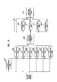
- FIG. 9 is a block diagram of the image processing unit according to the present exemplary embodiment.
- the RR′GBB′ mosaic image obtained from the five-color G checkered random arrangement is input to the image processing unit.
- a G interpolation unit 201 , an R interpolation unit 202 , an R′ interpolation unit 203 , a B interpolation unit 204 , and a B′ interpolation unit 205 generate a first RR′GBB′ interpolated image 206 which is an image in which pixel values of all the color are interpolated at all the pixel locations.
- an R MS-SyncNR unit 207 processes this first RR′GBB′ interpolated image 206 so as to generate a second RR′GBB′ interpolated image 211 as a final output.
- the G pixel value is interpolated at all the pixel locations.
- FIG. 10 is a flow chart of a process performed by the G interpolation unit 201 shown in FIG. 9 .
- the G interpolation unit 201 In a loop 302 , the G interpolation unit 201 repeatedly performs a process for each of the pixel locations. As used herein, a pixel that is subjected to the process in one loop is referred to as a “pixel of interest”.
- the G interpolation unit 201 reads out the pixel values of pixels in the vicinity of a pixel of interest in the mosaic image.
- the G interpolation unit 201 determines whether the filter color at the location of the pixel of interest is G.
- step ST 303 the G interpolation unit 201 determines that the filter color at the location of the pixel of interest is G, the processing proceeds to step ST 304 , where the pixel value of the pixel of interest is considered to be a G color pixel value.
- step ST 303 the G interpolation unit 201 determines that the filter color at the location of the pixel of interest is not G, the processing proceeds to step ST 305 .
- the G interpolation unit 201 computes a horizontal interpolation GH using the following equation:
- the G interpolation unit 201 interpolates a pixel value of the G color G(x, y) of the pixel of interest using GradH, GradV, GH, and GV according to the following equation:
- the interpolation process of the G pixel value of the pixel of interest is completed when the process at step ST 304 or ST 307 is completed. Thereafter, the next loop process for the location of the next pixel of interest starts. If the loop process for all the pixels is completed, the processing exits the loop 302 . Thus, the process performed by the G interpolation unit 201 is completed.
- R Interpolation Unit 202 R′ Interpolation Unit 203 , B Interpolation Unit 204 , and B′ Interpolation Unit 205
- the processes performed by the R interpolation unit 202 , the R′ interpolation unit 203 , the B interpolation unit 204 , and the B′ interpolation unit 205 are similar except regarding the target color. Accordingly, description is made with reference to only the R interpolation unit 202 . Descriptions of the R′ interpolation unit 203 , the B interpolation unit 204 , and the B′ interpolation unit 205 can be obtained by replacing the symbol “R” in the description of the R interpolation unit 202 with “R′”, “B”, and “B′”, respectively.
- FIG. 11 is a flow chart of a process performed by the R interpolation unit 202 shown in FIG. 9 . Hereinbelow, a procedure is described with reference to this flow chart.
- the R interpolation unit 202 repeatedly performs a process for each of the pixel locations.
- a pixel that is subjected to the process in one loop is referred to as a “pixel of interest”.
- the R interpolation unit 202 reads out the G pixel values of the pixels in the vicinity of a pixel of interest. Note that the pixel values were computed by the G interpolation unit 201 shown in FIG. 9 .
- the R interpolation unit 202 reads out the pixel values of pixels in the vicinity of the pixel of interest in the RR′GBB′ mosaic image.
- the R interpolation unit 202 computes a low-frequency component G low of the G color pixel, which is the pixel of interest.
- the R interpolation unit 202 computes a low-frequency component R low of the R color pixel, which is the pixel of interest.
- the R interpolation unit 202 interpolates an R pixel value R(x, y) of the pixel of interest using G low and R low , according to the following equation:
- R ⁇ ( x , y ) R low G low ⁇ G ⁇ ( x , y ) ( 7 )
- the interpolation process of the R pixel value of the pixel of interest is completed when the process at step ST 406 is completed. Thereafter, the next loop process for the location of the next pixel of interest starts. If the loop process for all the pixels is completed, the processing exits the loop 403 . Thus, the process performed by the R interpolation unit 202 is completed.
- FIG. 12A is a flow chart of a detailed process performed at step ST 404 shown in FIG. 11 .
- the G color pixels contained in a local region are averaged. That is, a low-pass filter using a finite impulse response (FIR) filter is formed.
- FIR finite impulse response
- the R interpolation unit 202 initializes G low to zero.
- the R interpolation unit 202 performs a loop process for each of the locations of all the pixels in a local region including the pixel of interest.
- local region refers to the above-described region having the predetermined size.
- a pixel that is subjected to the process in one loop is referred to as a “pixel of interest in the local region”.
- the R interpolation unit 202 multiplies G(s, t) by WG(s, t). Thereafter, the resultant value is added to G low . The resultant value is considered to be a new value of G low .
- G(s, t) denotes the pixel value of G color at the location (s, t) of a pixel of interest in the local region.
- WG(s, t) denotes a weighting coefficient.
- WG(s, t) is determined to be a coefficient for a low-pass filter and the sum of the coefficients is 1.
- the process for the pixel of interest in the local region is completed when the process at step ST 503 is completed. Thereafter, the next loop process for the next pixel of interest in the local region starts. If the loop process for all the pixels in the local region is completed, the processing exits the loop 502 . Thus, the process performed by the R interpolation unit 202 at step ST 404 is completed.
- FIG. 12B is a flow chart of a detailed process performed at step ST 405 shown in FIG. 11 .
- the R color pixels contained in the local region are averaged. That is, a low-pass filter using an FIR filter is formed.
- the R interpolation unit 202 initializes a variable R low to 0.
- the R interpolation unit 202 performs a loop process for each of the locations of all the pixels in a local region including the pixel of interest.
- the local region refers to the above-described region having the predetermined size.
- the R interpolation unit 202 determines whether the filter color at the location of the pixel of interest in the local region is R.
- step ST 603 the R interpolation unit 202 determines that the filter color at the location of the pixel of interest is R
- the processing proceeds to step ST 604 , where M(s, t) is multiplied by WR(s, t).
- the resultant value is added to R low .
- the resultant value is considered to be a new value of R low .
- M(s, t) denotes the pixel value at the location (s, t) of a pixel of interest in the local region.
- WR(s, t) denotes a weighting coefficient.
- WR(s, t) is determined to be a coefficient for a low-pass filter and the sum of the coefficients is 1.
- WR(s, t) is determined so that the characteristics of the low-pass filter composed of WR(s, t) are close to those of a low-pass filter composed of WG(s, t).
- the process for this pixel of interest in the local region is completed when the process at step ST 604 is completed. Thereafter, the next loop process for the next pixel of interest in the local region starts. If the loop process for all the pixels in the local region is completed, the processing exits the loop 602 . Thus, the process performed by the R interpolation unit 202 at step ST 405 is completed.
- the processes performed by the R MS-SyncNR unit 207 , the R′ MS-SyncNR unit 208 , the B MS-SyncNR unit 209 , and the B′ MS-SyncNR unit 210 are similar except regarding the target color. Accordingly, description is made with reference to only the R MS-SyncNR unit 207 . Descriptions of the R′ MS-SyncNR unit 208 , the B MS-SyncNR unit 209 , and the B′ MS-SyncNR unit 210 can be obtained by replacing the symbol “R” in the description of the R MS-SyncNR unit 207 with “R′”, “B”, and “B′”, respectively.
- FIG. 13 is a block diagram of a detailed structure of the R MS-SyncNR unit 207 shown in FIG. 9 .
- two G and R channels receive signals, and noise is removed from the R color signal. Thereafter, an output signal without noise is output from the structure. If a component that has no correlation with the R color signal is removed from the G color signal, the occurrence of a false color is eliminated. Accordingly, in the present exemplary embodiment, noise is not removed from the G color signal. However, in practical applications, it is desirable that noise is removed from the G color signal using some noise removing method and, subsequently, noise is removed from the R color signal by the method according to the present exemplary embodiment.
- the R MS-SyncNR unit 207 includes two multiple-resolution transform units 701 and 702 , a multiple-resolution inverse transform unit 717 , and correction units 711 , 712 , and 713 . Note that the number of correction units (three in FIG. 13 ) is determined by subtracting one from the number of layers of the multiple resolutions.
- the first multiple-resolution transform unit 701 converts an image input from the G channel to multiple-resolution image data. Thereafter, the multiple-resolution transform unit 701 stores image signals corresponding to the layers of the multiple resolutions in memories 703 , 704 , 705 , and 706 .
- the second multiple-resolution transform unit 702 converts an image input from the R channel to multiple-resolution image data. Thereafter, the multiple-resolution transform unit 702 stores image signals corresponding to the layers of the multiple resolutions in memories 707 , 708 , 709 , and 710 .
- the correction units 711 , 712 , and 713 correspond to layers other than the layer of the minimum resolution.
- Each of the correction units 711 , 712 , and 713 receives images of the G and R channels in the corresponding layer, corrects each of the pixels of the images that contain noise so as to generate an R channel image without noise, and stores the generated R channel image in the corresponding one of image memories 714 , 715 , and 716 .
- correction units 711 , 712 , and 713 are described in more detail next.
- correction units 711 , 712 , and 713 have a similar configuration and operate in a similar manner, only the correction unit 711 is described here.
- FIG. 14 is a block diagram illustrating an exemplary configuration of the correction unit 711 .
- the correction unit 711 includes sampling processing units 801 and 802 , a variance computing unit 803 , a clipping processing unit 804 , a divider processing unit 805 , a covariance computing unit 806 , and a multiplier processing unit 807 .
- the sampling processing unit 801 samples (extracts) a plurality of G channel pixel values from pixels in the vicinity of a predetermined location determined corresponding to the location of a pixel of interest. The sampling processing unit 801 then delivers the sampled G channel pixel values to the multiplier processing unit 807 , the variance computing unit 803 , and the covariance computing unit 806 .
- the sampling processing unit 802 samples (extracts) a plurality of R channel pixel values from pixels in the vicinity of a predetermined location determined corresponding to the location of a pixel of interest. The sampling processing unit 802 then delivers the sampled R channel pixel values to the covariance computing unit 806 . Note that the sampling processing units 801 and 802 extract the G pixel value and the R pixel value at the same location determined corresponding to the position of the pixel of interest.
- the variance computing unit 803 computes the variance of the G pixel values in the vicinity of the pixel of interest on the basis of the sampled G pixel values. Thereafter, the variance computing unit 803 delivers the computed variance to the clipping processing unit 804 .
- the covariance computing unit 806 computes the covariance of the G pixel values and the R pixel values on the basis of the sampled G and R pixels values. The covariance computing unit 806 then delivers the computed covariance to the divider processing unit 805 . If the variance of the samples of the G channel is less than a predetermined threshold value, the clipping processing unit 804 clips the variance to the predetermined threshold value and delivers that value to the divider processing unit 805 . The divider processing unit 805 divides the covariance delivered from the covariance computing unit 806 by the variance delivered from the clipping processing unit 804 .
- the divider processing unit 805 delivers the ratio of the covariance to the variance (i.e., the covariance/the variance) to the multiplier processing unit 807 .
- the above-described process performed by the clipping processing unit 804 prevents the occurrence of the ratio of zero when the divider processing unit 805 performs the subsequent process (i.e., the computation of the covariance/the variance).
- the multiplier processing unit 807 estimates the R channel pixel value of the pixel of interest without noise and outputs the estimated value.
- correction units 711 , 712 , and 713 are described in detail next.
- the correction units 711 , 712 , and 713 correct pixel values by a pixel value estimation method using a correlation between channels. More specifically, on ground that there is a linear relationship between two channels (e.g., G and R) when focusing on a local region, the estimation value of R at a pixel location in the local region is obtained by a linear regression computation.
- a luminance estimation value C 2C ′ of the C 2 channel at the location of the pixel of interest can be obtained using a luminance estimation value C 1C of the C 1 channel at the location of the pixel of interest according to the following equation:
- C 2 ⁇ c ′ V C 1 ⁇ C 2 V C 1 ⁇ C 1 ⁇ ( C 1 ⁇ c - M C 1 ) + M C 2 ( 8 )
- M C1 denotes the expectation value of the C 1 channel in the local region
- M C2 denotes the expectation value of the C 2 channel
- V C1C2 is the covariance of the C 1 and C 2 channels
- V C1C1 is the variance of the C 1 channel.
- the samples are the pixel values of a plurality of pixels at predetermined locations corresponding to the location of the pixel of interest.
- w i denotes a predetermined weighting coefficient
- the R MS-SyncNR unit 207 includes the resolution transform units 701 and 702 . Therefore, the correction unit 711 corrects the pixel values for images separated for each of frequency ranges using the above-described correlation between two channels.
- equations (8) to (10) are replaced by the following equations (11) to (13):
- C 2 ⁇ c ′ V C 1 ⁇ C 2 V C 1 ⁇ C 1 ⁇ C 1 ⁇ c ( 11 )
- the variance computing unit 803 shown in FIG. 14 computes the variance using equation (13).
- the covariance computing unit 806 computes the covariance using equation (12).
- the multiplier processing unit 807 modifies (corrects) the pixel values using equation (11).
- an approximate function may be used.
- the number of the multiplication processing operations may be reduced.
- the following approximate functions may be used:
- the multiple resolution inverse transform unit 717 receives the R channel images without noise in the layers and the R channel image in the minimum-resolution layer and combines all the R channel images into an image having the same resolution as that of the original image. Subsequently, the multiple resolution inverse transform unit 717 outputs the combined image.
- a color filter arrangement used for a single-plate color imaging device is defined in which filters of four or more color are included, the filters of some of the colors are regularly arranged, and filters of the other colors are randomly arranged.
- an image processing unit includes a color filter array having such an arrangement.
- the color filter array having such an arrangement uses the number of colors more than that used in the Bayer arrangement, and therefore, can improve the performance of the color reproduction and the dynamic range.
- the color filter array since the color filter array includes regularly arranged color filters, the color filter array can provide the resolution that is the same as that of the Bayer arrangement. Additionally, by using a random filter arrangement and the R MS-SyncNR unit 207 , the R′ MS-SyncNR unit 208 , the B MS-SyncNR unit 209 , and the B′ MS-SyncNR unit 210 shown in FIG. 9 , this color filter array can efficiently reduce the occurrence of a false color.
- the C 1 color occupies a half of the total number of pixels in a mosaic image obtained through the color filter array, the C 1 color has a resolution higher than that of the other color. Accordingly, the C 1 color is allocated to the positions of all the pixels first. Subsequently, high-frequency components of the other colors are estimated (interpolated) using the allocated C 1 color as a reference. In this way, an image with high resolution for all the colors can be obtained after the interpolation is performed.
- a reference channel e.g., G
- estimation is performed so that the correlation of the other channel signal with respect to the reference signal is the highest on the basis of the same idea as the pixel value estimation method using a correlation between channels.
- a low correlation between channels results in an image having false colors distributed in a variety of spatial frequency ranges. Therefore, by increasing the correlation between channels using the R MS-SyncNR unit 207 , the R′ MS-SyncNR unit 208 , the B MS-SyncNR unit 209 , and the B′ MS-SyncNR unit 210 , the occurrence of the false color can be eliminated.
- the arrangement of the color filter array can be considered to be the same as the Bayer arrangement when a dumping readout process or a summing readout process is performed.
- a color filter arrangement is obtained by replacing the C 1 color filters arranged in a checkered pattern in the color filter arrangement according to the first exemplary embodiment with regularly arranged filters of two colors C 1 a and C 1 b.
- a new color C 1 c is generated on the basis of the colors C 1 a and C 1 b . Thereafter, using the regular arrangement of the C 1 a and C 1 b color filters, the color C 1 c can be interpolated at the locations of all of the pixels at which the C 1 a or C 1 b color filters are present.
- the filter arrangement in which the C 1 c color filters are arranged in place of the C 1 a and C 1 b color filters is the same as the filter arrangement described in the first exemplary embodiment.
- the color filter array provides the same advantage as that of the first exemplary embodiment.
- the number of filter colors is incremented by one compared with the first exemplary embodiment, the performance of color reproduction and the dynamic range can be further improved.
- FIG. 15 illustrates an exemplary structure of the color filter array according to the second exemplary embodiment.
- the filters of two colors G and G′ are arranged in a checkered pattern and the filters of other four colors are arranged in a random pattern.
- FIG. 16 illustrates a demosaic process performed when the color filter array shown in FIG. 15 is used.
- the image processing unit When compared with the image processing unit shown in FIG. 9 , as shown in FIG. 16 , the image processing unit according to the present exemplary embodiment includes a (G+G′) interpolation unit a 201 in place of the G interpolation unit 201 . Additionally, processes similar to those performed by the R interpolation unit 202 , the R′ interpolation unit 203 , the B interpolation unit 204 , and the B′ interpolation unit 205 are added to the processes for the G and G′ colors (i.e., a G interpolation unit a 202 and a G′ interpolation unit a 203 ). Thus, a six-plane image (i.e., a first RR′GG′BB′ interpolation image a 208 ) is generated instead of a five-plane image.
- a six-plane image i.e., a first RR′GG′BB′ interpolation image a 208
- the MS-SyncNR process is performed on each of the R, R′, B, and B′ color images.
- FIG. 17 illustrates a modification of the color filter array according to the present exemplary embodiment.
- filters of two colors G and G′ are arranged in a checkered pattern
- filters of a color R are arranged on every other pixel in the horizontal direction and the vertical direction
- filters of the other two colors are randomly arranged.
- the performance of color reproduction and the dynamic range can be further improved.
- the correlation of spectral sensitivity between the colors C 1 a and C 1 b is higher than that between the other colors. That is, as described in Japanese Unexamined Patent Application Publication No. 2005-160044, when a new color C 1 c is generated on the basis of the C 1 a and C 1 b colors using the regular arrangement of the C 1 a and C 1 b color filters, it is desirable that the correlation of spectral sensitivity between the C 1 a and C 1 b color filters is high.
- a new color C 1 c is computed using the colors C 1 a and C 1 b.
- the image processing unit estimates (interpolates) the pixel value of the C 1 b color at the position of the pixel of interest using the C 1 a and C 1 b colors that are present in the local region including the position of the pixel of interest.
- the image processing unit interpolates the pixel value of the C 1 a color at the position of the pixel of interest using the C 1 a and C 1 b colors that are present in the local region including the position of the pixel of interest.
- the image processing unit computes the pixel values of the color C 1 c at the locations of pixels arranged in a checkered pattern from the pixel values of the colors C 1 a and C 1 b at those locations.
- the image processing unit interpolates the pixel values of the color C 1 c at pixel locations at which the color C 1 c is not present using the pixel values of the color C 1 c present around the pixel locations.
- the image processing unit interpolates a color CX other than the color C 1 c using the pixel values of the colors C 1 c and CX that are present in the local region including the position of the pixel of interest.
- the image processing unit includes an R MS-SyncNR unit a 209 , an R′ MS-SyncNR unit a 210 , a B MS-SyncNR unit a 211 , and a B′ MS-SyncNR unit a 212 .
- the new color C 1 c may be generated on the basis of the regularly arranged color filters C 1 a and C 1 b . Thereafter, the color C 1 c can be interpolated for all the pixels on which the color C 1 a or C 1 b is present.
- the present exemplary embodiment can provide the advantages that are the same as those of the first exemplary embodiment.
Abstract
Description
GradH=|M(x−1,y)−M(x+1,y)| (2)
where M(x, y) represents the pixel value at a location (x, y) of the pixel of interest.
GradH=|M(x,y−1)−M(x,y+1)| (4)
Subsequently, the
where MC1 denotes the expectation value of the C1 channel in the local region, MC2 denotes the expectation value of the C2 channel, VC1C2 is the covariance of the C1 and C2 channels, and VC1C1 is the variance of the C1 channel. Note that the samples are the pixel values of a plurality of pixels at predetermined locations corresponding to the location of the pixel of interest.
Claims (13)
Priority Applications (2)
| Application Number | Priority Date | Filing Date | Title |
|---|---|---|---|
| US12/586,000 US8339487B2 (en) | 2006-03-14 | 2009-09-30 | Color filter array, imaging device, and image processing unit |
| US13/682,223 US20130140436A1 (en) | 2006-03-14 | 2012-11-20 | Color Filter Array, Imaging Device, and Image Processing Unit |
Applications Claiming Priority (2)
| Application Number | Priority Date | Filing Date | Title |
|---|---|---|---|
| JP2006069541A JP5183880B2 (en) | 2006-03-14 | 2006-03-14 | Color filter and image sensor |
| JP2006-069541 | 2006-03-14 |
Related Child Applications (1)
| Application Number | Title | Priority Date | Filing Date |
|---|---|---|---|
| US12/586,000 Division US8339487B2 (en) | 2006-03-14 | 2009-09-30 | Color filter array, imaging device, and image processing unit |
Publications (2)
| Publication Number | Publication Date |
|---|---|
| US20070216785A1 US20070216785A1 (en) | 2007-09-20 |
| US7710476B2 true US7710476B2 (en) | 2010-05-04 |
Family
ID=38517358
Family Applications (3)
| Application Number | Title | Priority Date | Filing Date |
|---|---|---|---|
| US11/714,261 Expired - Fee Related US7710476B2 (en) | 2006-03-14 | 2007-03-06 | Color filter array, imaging device, and image processing unit |
| US12/586,000 Expired - Fee Related US8339487B2 (en) | 2006-03-14 | 2009-09-30 | Color filter array, imaging device, and image processing unit |
| US13/682,223 Abandoned US20130140436A1 (en) | 2006-03-14 | 2012-11-20 | Color Filter Array, Imaging Device, and Image Processing Unit |
Family Applications After (2)
| Application Number | Title | Priority Date | Filing Date |
|---|---|---|---|
| US12/586,000 Expired - Fee Related US8339487B2 (en) | 2006-03-14 | 2009-09-30 | Color filter array, imaging device, and image processing unit |
| US13/682,223 Abandoned US20130140436A1 (en) | 2006-03-14 | 2012-11-20 | Color Filter Array, Imaging Device, and Image Processing Unit |
Country Status (2)
| Country | Link |
|---|---|
| US (3) | US7710476B2 (en) |
| JP (1) | JP5183880B2 (en) |
Cited By (5)
| Publication number | Priority date | Publication date | Assignee | Title |
|---|---|---|---|---|
| US20080130073A1 (en) * | 2006-12-01 | 2008-06-05 | Compton John T | Light sensitivity in image sensors |
| US20090091646A1 (en) * | 2007-10-03 | 2009-04-09 | Canon Kabushiki Kaisha | Color processing apparatus and method thereof |
| US20100053385A1 (en) * | 2008-08-27 | 2010-03-04 | Won-Hee Choe | Apparatus and method of generating a high dynamic range image |
| US20150042999A1 (en) * | 2011-07-28 | 2015-02-12 | Asml Netherlands B.V. | Illumination Source for use in Inspection Methods and/or Lithography; Inspection and Lithographic Apparatus and Inspection Method |
| US20150109494A1 (en) * | 2012-07-06 | 2015-04-23 | Fujifilm Corporation | Color imaging element and imaging device |
Families Citing this family (36)
| Publication number | Priority date | Publication date | Assignee | Title |
|---|---|---|---|---|
| US8049797B2 (en) * | 2007-05-08 | 2011-11-01 | Canon Kabushiki Kaisha | Image sensor and color imaging apparatus |
| TWI394429B (en) * | 2009-07-27 | 2013-04-21 | Altek Corp | Method for eliminating image's noise and apparatus using the method |
| US8294781B2 (en) * | 2009-10-20 | 2012-10-23 | Apple Inc. | System and method for sharpening image data |
| US8638342B2 (en) * | 2009-10-20 | 2014-01-28 | Apple Inc. | System and method for demosaicing image data using weighted gradients |
| US8259198B2 (en) * | 2009-10-20 | 2012-09-04 | Apple Inc. | System and method for detecting and correcting defective pixels in an image sensor |
| US8593483B2 (en) * | 2009-10-20 | 2013-11-26 | Apple Inc. | Temporal filtering techniques for image signal processing |
| US8472712B2 (en) * | 2009-10-20 | 2013-06-25 | Apple Inc. | System and method for applying lens shading correction during image processing |
| KR101641543B1 (en) * | 2010-02-05 | 2016-07-21 | 삼성전자주식회사 | Apparatus and method for reducing noise of color image |
| US20110205411A1 (en) * | 2010-02-25 | 2011-08-25 | German Voronov | Pixel arrays, image sensors, image sensing systems and digital imaging systems having reduced line noise |
| JP4991907B2 (en) * | 2010-05-11 | 2012-08-08 | キヤノン株式会社 | Image processing apparatus and method for controlling image processing apparatus |
| US8692906B2 (en) * | 2010-07-13 | 2014-04-08 | Canon Kabushiki Kaisha | Luminance signal generation apparatus, luminance signal generation method, image pickup apparatus, and storage medium |
| JP5675215B2 (en) * | 2010-08-20 | 2015-02-25 | オリンパス株式会社 | Digital camera |
| US8471932B2 (en) | 2010-09-30 | 2013-06-25 | Apple Inc. | Spatial filtering for image signal processing |
| US8508612B2 (en) | 2010-09-30 | 2013-08-13 | Apple Inc. | Image signal processor line buffer configuration for processing ram image data |
| JP5677040B2 (en) | 2010-11-08 | 2015-02-25 | キヤノン株式会社 | Image processing apparatus and control method thereof |
| US8917336B2 (en) | 2012-05-31 | 2014-12-23 | Apple Inc. | Image signal processing involving geometric distortion correction |
| US9031319B2 (en) | 2012-05-31 | 2015-05-12 | Apple Inc. | Systems and methods for luma sharpening |
| US9332239B2 (en) | 2012-05-31 | 2016-05-03 | Apple Inc. | Systems and methods for RGB image processing |
| US11089247B2 (en) | 2012-05-31 | 2021-08-10 | Apple Inc. | Systems and method for reducing fixed pattern noise in image data |
| US9014504B2 (en) | 2012-05-31 | 2015-04-21 | Apple Inc. | Systems and methods for highlight recovery in an image signal processor |
| US9105078B2 (en) | 2012-05-31 | 2015-08-11 | Apple Inc. | Systems and methods for local tone mapping |
| US8953882B2 (en) | 2012-05-31 | 2015-02-10 | Apple Inc. | Systems and methods for determining noise statistics of image data |
| US8817120B2 (en) | 2012-05-31 | 2014-08-26 | Apple Inc. | Systems and methods for collecting fixed pattern noise statistics of image data |
| US9142012B2 (en) | 2012-05-31 | 2015-09-22 | Apple Inc. | Systems and methods for chroma noise reduction |
| US9077943B2 (en) | 2012-05-31 | 2015-07-07 | Apple Inc. | Local image statistics collection |
| US9025867B2 (en) | 2012-05-31 | 2015-05-05 | Apple Inc. | Systems and methods for YCC image processing |
| US8872946B2 (en) | 2012-05-31 | 2014-10-28 | Apple Inc. | Systems and methods for raw image processing |
| US9743057B2 (en) | 2012-05-31 | 2017-08-22 | Apple Inc. | Systems and methods for lens shading correction |
| JP6097524B2 (en) * | 2012-10-29 | 2017-03-15 | キヤノン株式会社 | Image processing method, image processing apparatus, and program |
| KR101744761B1 (en) * | 2012-11-30 | 2017-06-09 | 한화테크윈 주식회사 | Method and Apparatus for processing image |
| JP6368115B2 (en) | 2013-05-10 | 2018-08-01 | キヤノン株式会社 | Solid-state imaging device and camera |
| WO2014188950A1 (en) * | 2013-05-23 | 2014-11-27 | 富士フイルム株式会社 | Pixel interpolation device and operation control method |
| US9692992B2 (en) * | 2013-07-01 | 2017-06-27 | Omnivision Technologies, Inc. | Color and infrared filter array patterns to reduce color aliasing |
| EP3444675A1 (en) * | 2017-08-14 | 2019-02-20 | ASML Netherlands B.V. | Optical detector |
| JP2019080245A (en) | 2017-10-26 | 2019-05-23 | ソニーセミコンダクタソリューションズ株式会社 | Image processing device, image processing method, and imaging device |
| WO2020241427A1 (en) * | 2019-05-31 | 2020-12-03 | ソニー株式会社 | Imaging device, electronic apparatus, information processing method, and program |
Citations (11)
| Publication number | Priority date | Publication date | Assignee | Title |
|---|---|---|---|---|
| US3971065A (en) | 1975-03-05 | 1976-07-20 | Eastman Kodak Company | Color imaging array |
| US4716455A (en) | 1985-03-25 | 1987-12-29 | Hitachi, Ltd. | Chrominance signal interpolation device for a color camera |
| US5552827A (en) | 1993-08-31 | 1996-09-03 | Sanyo Electric Co., Ltd. | Color video camera with a solid state image sensing device |
| EP0804037A2 (en) | 1996-04-25 | 1997-10-29 | Eastman Kodak Company | Process and system for generating a full color image or multispectral image from the image data of a CCD image sensor with a mosaic color filter. |
| JP2000316169A (en) | 1999-05-06 | 2000-11-14 | Olympus Optical Co Ltd | Color image pickup element and device |
| US20040174446A1 (en) * | 2003-02-28 | 2004-09-09 | Tinku Acharya | Four-color mosaic pattern for depth and image capture |
| US6803955B1 (en) * | 1999-03-03 | 2004-10-12 | Olympus Corporation | Imaging device and imaging apparatus |
| JP2005160044A (en) | 2003-10-31 | 2005-06-16 | Sony Corp | Image processing apparatus, image processing method, and program |
| US20060198556A1 (en) * | 1999-12-21 | 2006-09-07 | Nikon Corporation | Interpolation processing apparatus and recording medium having interpolation processing program recording therein |
| US7123299B1 (en) * | 1999-04-15 | 2006-10-17 | Olympus Optical Co., Ltd. | Color image pickup device and color image pickup apparatus including a randomized color coding array |
| US20070296841A1 (en) * | 2006-03-14 | 2007-12-27 | Yoshikuni Nomura | Method and apparatus for manufacturing color image pickup device |
Family Cites Families (7)
| Publication number | Priority date | Publication date | Assignee | Title |
|---|---|---|---|---|
| JPS58168017A (en) * | 1982-03-29 | 1983-10-04 | Mitsubishi Electric Corp | Solid-state image pickup element |
| JP3724882B2 (en) * | 1996-08-14 | 2005-12-07 | シャープ株式会社 | Color solid-state imaging device |
| JP2000316168A (en) * | 1999-05-06 | 2000-11-14 | Olympus Optical Co Ltd | Color image pickup element and device |
| JP4094364B2 (en) * | 2002-07-19 | 2008-06-04 | 富士フイルム株式会社 | Solid-state imaging device and photometric method thereof |
| JP4385282B2 (en) * | 2003-10-31 | 2009-12-16 | ソニー株式会社 | Image processing apparatus and image processing method |
| JP2005354610A (en) * | 2004-06-14 | 2005-12-22 | Canon Inc | Image processing apparatus, image processing method and image processing program |
| JP4587450B2 (en) * | 2004-07-29 | 2010-11-24 | 富士フイルム株式会社 | Solid-state imaging device |
-
2006
- 2006-03-14 JP JP2006069541A patent/JP5183880B2/en not_active Expired - Fee Related
-
2007
- 2007-03-06 US US11/714,261 patent/US7710476B2/en not_active Expired - Fee Related
-
2009
- 2009-09-30 US US12/586,000 patent/US8339487B2/en not_active Expired - Fee Related
-
2012
- 2012-11-20 US US13/682,223 patent/US20130140436A1/en not_active Abandoned
Patent Citations (13)
| Publication number | Priority date | Publication date | Assignee | Title |
|---|---|---|---|---|
| US3971065A (en) | 1975-03-05 | 1976-07-20 | Eastman Kodak Company | Color imaging array |
| US4716455A (en) | 1985-03-25 | 1987-12-29 | Hitachi, Ltd. | Chrominance signal interpolation device for a color camera |
| US5552827A (en) | 1993-08-31 | 1996-09-03 | Sanyo Electric Co., Ltd. | Color video camera with a solid state image sensing device |
| JP2931520B2 (en) | 1993-08-31 | 1999-08-09 | 三洋電機株式会社 | Color separation circuit for single-chip color video camera |
| EP0804037A2 (en) | 1996-04-25 | 1997-10-29 | Eastman Kodak Company | Process and system for generating a full color image or multispectral image from the image data of a CCD image sensor with a mosaic color filter. |
| US5889554A (en) * | 1996-04-25 | 1999-03-30 | Eastman Kodak Company | Process and system for generating a full color image of multispectral image from the image data of a CCD image sensor with a mosaic color filter |
| US6803955B1 (en) * | 1999-03-03 | 2004-10-12 | Olympus Corporation | Imaging device and imaging apparatus |
| US7123299B1 (en) * | 1999-04-15 | 2006-10-17 | Olympus Optical Co., Ltd. | Color image pickup device and color image pickup apparatus including a randomized color coding array |
| JP2000316169A (en) | 1999-05-06 | 2000-11-14 | Olympus Optical Co Ltd | Color image pickup element and device |
| US20060198556A1 (en) * | 1999-12-21 | 2006-09-07 | Nikon Corporation | Interpolation processing apparatus and recording medium having interpolation processing program recording therein |
| US20040174446A1 (en) * | 2003-02-28 | 2004-09-09 | Tinku Acharya | Four-color mosaic pattern for depth and image capture |
| JP2005160044A (en) | 2003-10-31 | 2005-06-16 | Sony Corp | Image processing apparatus, image processing method, and program |
| US20070296841A1 (en) * | 2006-03-14 | 2007-12-27 | Yoshikuni Nomura | Method and apparatus for manufacturing color image pickup device |
Cited By (9)
| Publication number | Priority date | Publication date | Assignee | Title |
|---|---|---|---|---|
| US20080130073A1 (en) * | 2006-12-01 | 2008-06-05 | Compton John T | Light sensitivity in image sensors |
| US20090091646A1 (en) * | 2007-10-03 | 2009-04-09 | Canon Kabushiki Kaisha | Color processing apparatus and method thereof |
| US7986361B2 (en) * | 2007-10-03 | 2011-07-26 | Canon Kabushiki Kaisha | Color processing apparatus and method thereof for generating an interpolated image |
| US20100053385A1 (en) * | 2008-08-27 | 2010-03-04 | Won-Hee Choe | Apparatus and method of generating a high dynamic range image |
| US8294797B2 (en) * | 2008-08-27 | 2012-10-23 | Samsung Electronics Co., Ltd. | Apparatus and method of generating a high dynamic range image |
| US20150042999A1 (en) * | 2011-07-28 | 2015-02-12 | Asml Netherlands B.V. | Illumination Source for use in Inspection Methods and/or Lithography; Inspection and Lithographic Apparatus and Inspection Method |
| US9632424B2 (en) * | 2011-07-28 | 2017-04-25 | Asml Netherlands B.V. | Illumination source for use in inspection methods and/or lithography; inspection and lithographic apparatus and inspection method |
| US20150109494A1 (en) * | 2012-07-06 | 2015-04-23 | Fujifilm Corporation | Color imaging element and imaging device |
| US9184196B2 (en) * | 2012-07-06 | 2015-11-10 | Fujifilm Corporation | Color imaging element and imaging device |
Also Published As
| Publication number | Publication date |
|---|---|
| JP5183880B2 (en) | 2013-04-17 |
| US20070216785A1 (en) | 2007-09-20 |
| US20100091147A1 (en) | 2010-04-15 |
| US20130140436A1 (en) | 2013-06-06 |
| US8339487B2 (en) | 2012-12-25 |
| JP2007251393A (en) | 2007-09-27 |
Similar Documents
| Publication | Publication Date | Title |
|---|---|---|
| US7710476B2 (en) | Color filter array, imaging device, and image processing unit | |
| US7701496B2 (en) | Color filter pattern for color filter arrays including a demosaicking algorithm | |
| US8467088B2 (en) | Image signal processing apparatus, imaging apparatus, image signal processing method and computer program | |
| US10136107B2 (en) | Imaging systems with visible light sensitive pixels and infrared light sensitive pixels | |
| US8891866B2 (en) | Image processing apparatus, image processing method, and program | |
| JP4351825B2 (en) | How to collect color digital images | |
| US8462220B2 (en) | Method and apparatus for improving low-light performance for small pixel image sensors | |
| US7148925B2 (en) | Solid-state honeycomb type image pickup apparatus using a complementary color filter and signal processing method therefor | |
| US8270774B2 (en) | Image processing device for performing interpolation | |
| EP3038356A1 (en) | Exposing pixel groups in producing digital images | |
| EP2323408A1 (en) | Image processing device, image processing method, image capturing device, and computer program | |
| US9338364B2 (en) | Imaging device and image generation method | |
| US6133953A (en) | Color camera having a single imaging element and capable of restricting unwanted false color signal | |
| US6469290B1 (en) | Solid-state image pickup apparatus in compliance with the arrangement of complementary color filter segments and a signal processing method therefor | |
| JP2004153823A (en) | Image processing system using local linear regression | |
| JP2000134634A (en) | Image converting method | |
| KR20210018136A (en) | Method and apparatus for image processing | |
| US8233733B2 (en) | Image processing device | |
| JP2014158267A (en) | Color filter, imaging element, image processing device, and image processing method | |
| JP4725520B2 (en) | Image processing device, non-imaging color signal calculation device, and image processing method | |
| US20030122937A1 (en) | Method for processing digital CFA images, particularly for motion and still imaging | |
| US20050134705A1 (en) | Digital image processing apparatus and method thereof | |
| KR101243285B1 (en) | Apparatus and method for reconstructing color image based on multi-spectrum using Bayer Color Filter Array camera | |
| JP2004056640A (en) | Interpolation method of photographed images in complementary color single ccd color digital camera, interpolation unit of the same, and digital camera comprising the same | |
| JP5195957B2 (en) | Color filter and image sensor |
Legal Events
| Date | Code | Title | Description |
|---|---|---|---|
| AS | Assignment |
Owner name: SONY CORPORATION,JAPAN Free format text: ASSIGNMENT OF ASSIGNORS INTEREST;ASSIGNORS:NOMURA, YOSHIKUNI;MITSUNAGA, TOMOO;SIGNING DATES FROM 20070416 TO 20070418;REEL/FRAME:019343/0383 Owner name: SONY CORPORATION, JAPAN Free format text: ASSIGNMENT OF ASSIGNORS INTEREST;ASSIGNORS:NOMURA, YOSHIKUNI;MITSUNAGA, TOMOO;REEL/FRAME:019343/0383;SIGNING DATES FROM 20070416 TO 20070418 |
|
| FEPP | Fee payment procedure |
Free format text: PAYOR NUMBER ASSIGNED (ORIGINAL EVENT CODE: ASPN); ENTITY STATUS OF PATENT OWNER: LARGE ENTITY |
|
| STCF | Information on status: patent grant |
Free format text: PATENTED CASE |
|
| CC | Certificate of correction | ||
| FPAY | Fee payment |
Year of fee payment: 4 |
|
| MAFP | Maintenance fee payment |
Free format text: PAYMENT OF MAINTENANCE FEE, 8TH YEAR, LARGE ENTITY (ORIGINAL EVENT CODE: M1552) Year of fee payment: 8 |
|
| FEPP | Fee payment procedure |
Free format text: MAINTENANCE FEE REMINDER MAILED (ORIGINAL EVENT CODE: REM.); ENTITY STATUS OF PATENT OWNER: LARGE ENTITY |
|
| LAPS | Lapse for failure to pay maintenance fees |
Free format text: PATENT EXPIRED FOR FAILURE TO PAY MAINTENANCE FEES (ORIGINAL EVENT CODE: EXP.); ENTITY STATUS OF PATENT OWNER: LARGE ENTITY |
|
| STCH | Information on status: patent discontinuation |
Free format text: PATENT EXPIRED DUE TO NONPAYMENT OF MAINTENANCE FEES UNDER 37 CFR 1.362 |
|
| FP | Lapsed due to failure to pay maintenance fee |
Effective date: 20220504 |