US7691313B2 - Method for expelling gas positioned between a substrate and a mold - Google Patents
Method for expelling gas positioned between a substrate and a mold Download PDFInfo
- Publication number
- US7691313B2 US7691313B2 US11/565,393 US56539306A US7691313B2 US 7691313 B2 US7691313 B2 US 7691313B2 US 56539306 A US56539306 A US 56539306A US 7691313 B2 US7691313 B2 US 7691313B2
- Authority
- US
- United States
- Prior art keywords
- substrate
- mold assembly
- region
- mold
- template
- Prior art date
- Legal status (The legal status is an assumption and is not a legal conclusion. Google has not performed a legal analysis and makes no representation as to the accuracy of the status listed.)
- Expired - Lifetime, expires
Links
Images


Classifications
-
- G—PHYSICS
- G03—PHOTOGRAPHY; CINEMATOGRAPHY; ANALOGOUS TECHNIQUES USING WAVES OTHER THAN OPTICAL WAVES; ELECTROGRAPHY; HOLOGRAPHY
- G03F—PHOTOMECHANICAL PRODUCTION OF TEXTURED OR PATTERNED SURFACES, e.g. FOR PRINTING, FOR PROCESSING OF SEMICONDUCTOR DEVICES; MATERIALS THEREFOR; ORIGINALS THEREFOR; APPARATUS SPECIALLY ADAPTED THEREFOR
- G03F7/00—Photomechanical, e.g. photolithographic, production of textured or patterned surfaces, e.g. printing surfaces; Materials therefor, e.g. comprising photoresists; Apparatus specially adapted therefor
- G03F7/70—Microphotolithographic exposure; Apparatus therefor
- G03F7/708—Construction of apparatus, e.g. environment aspects, hygiene aspects or materials
- G03F7/70858—Environment aspects, e.g. pressure of beam-path gas, temperature
- G03F7/70866—Environment aspects, e.g. pressure of beam-path gas, temperature of mask or workpiece
- G03F7/70875—Temperature, e.g. temperature control of masks or workpieces via control of stage temperature
-
- B—PERFORMING OPERATIONS; TRANSPORTING
- B29—WORKING OF PLASTICS; WORKING OF SUBSTANCES IN A PLASTIC STATE IN GENERAL
- B29C—SHAPING OR JOINING OF PLASTICS; SHAPING OF MATERIAL IN A PLASTIC STATE, NOT OTHERWISE PROVIDED FOR; AFTER-TREATMENT OF THE SHAPED PRODUCTS, e.g. REPAIRING
- B29C43/00—Compression moulding, i.e. applying external pressure to flow the moulding material; Apparatus therefor
- B29C43/003—Compression moulding, i.e. applying external pressure to flow the moulding material; Apparatus therefor characterised by the choice of material
-
- B—PERFORMING OPERATIONS; TRANSPORTING
- B29—WORKING OF PLASTICS; WORKING OF SUBSTANCES IN A PLASTIC STATE IN GENERAL
- B29C—SHAPING OR JOINING OF PLASTICS; SHAPING OF MATERIAL IN A PLASTIC STATE, NOT OTHERWISE PROVIDED FOR; AFTER-TREATMENT OF THE SHAPED PRODUCTS, e.g. REPAIRING
- B29C43/00—Compression moulding, i.e. applying external pressure to flow the moulding material; Apparatus therefor
- B29C43/02—Compression moulding, i.e. applying external pressure to flow the moulding material; Apparatus therefor of articles of definite length, i.e. discrete articles
- B29C43/021—Compression moulding, i.e. applying external pressure to flow the moulding material; Apparatus therefor of articles of definite length, i.e. discrete articles characterised by the shape of the surface
-
- B—PERFORMING OPERATIONS; TRANSPORTING
- B29—WORKING OF PLASTICS; WORKING OF SUBSTANCES IN A PLASTIC STATE IN GENERAL
- B29C—SHAPING OR JOINING OF PLASTICS; SHAPING OF MATERIAL IN A PLASTIC STATE, NOT OTHERWISE PROVIDED FOR; AFTER-TREATMENT OF THE SHAPED PRODUCTS, e.g. REPAIRING
- B29C43/00—Compression moulding, i.e. applying external pressure to flow the moulding material; Apparatus therefor
- B29C43/32—Component parts, details or accessories; Auxiliary operations
- B29C43/36—Moulds for making articles of definite length, i.e. discrete articles
-
- B—PERFORMING OPERATIONS; TRANSPORTING
- B29—WORKING OF PLASTICS; WORKING OF SUBSTANCES IN A PLASTIC STATE IN GENERAL
- B29D—PRODUCING PARTICULAR ARTICLES FROM PLASTICS OR FROM SUBSTANCES IN A PLASTIC STATE
- B29D11/00—Producing optical elements, e.g. lenses or prisms
- B29D11/00009—Production of simple or compound lenses
- B29D11/00365—Production of microlenses
-
- G—PHYSICS
- G03—PHOTOGRAPHY; CINEMATOGRAPHY; ANALOGOUS TECHNIQUES USING WAVES OTHER THAN OPTICAL WAVES; ELECTROGRAPHY; HOLOGRAPHY
- G03B—APPARATUS OR ARRANGEMENTS FOR TAKING PHOTOGRAPHS OR FOR PROJECTING OR VIEWING THEM; APPARATUS OR ARRANGEMENTS EMPLOYING ANALOGOUS TECHNIQUES USING WAVES OTHER THAN OPTICAL WAVES; ACCESSORIES THEREFOR
- G03B27/00—Photographic printing apparatus
- G03B27/32—Projection printing apparatus, e.g. enlarger, copying camera
- G03B27/52—Details
- G03B27/62—Holders for the original
-
- G—PHYSICS
- G03—PHOTOGRAPHY; CINEMATOGRAPHY; ANALOGOUS TECHNIQUES USING WAVES OTHER THAN OPTICAL WAVES; ELECTROGRAPHY; HOLOGRAPHY
- G03F—PHOTOMECHANICAL PRODUCTION OF TEXTURED OR PATTERNED SURFACES, e.g. FOR PRINTING, FOR PROCESSING OF SEMICONDUCTOR DEVICES; MATERIALS THEREFOR; ORIGINALS THEREFOR; APPARATUS SPECIALLY ADAPTED THEREFOR
- G03F7/00—Photomechanical, e.g. photolithographic, production of textured or patterned surfaces, e.g. printing surfaces; Materials therefor, e.g. comprising photoresists; Apparatus specially adapted therefor
- G03F7/70—Microphotolithographic exposure; Apparatus therefor
- G03F7/70691—Handling of masks or workpieces
- G03F7/707—Chucks, e.g. chucking or un-chucking operations or structural details
-
- B—PERFORMING OPERATIONS; TRANSPORTING
- B29—WORKING OF PLASTICS; WORKING OF SUBSTANCES IN A PLASTIC STATE IN GENERAL
- B29C—SHAPING OR JOINING OF PLASTICS; SHAPING OF MATERIAL IN A PLASTIC STATE, NOT OTHERWISE PROVIDED FOR; AFTER-TREATMENT OF THE SHAPED PRODUCTS, e.g. REPAIRING
- B29C43/00—Compression moulding, i.e. applying external pressure to flow the moulding material; Apparatus therefor
- B29C43/02—Compression moulding, i.e. applying external pressure to flow the moulding material; Apparatus therefor of articles of definite length, i.e. discrete articles
- B29C43/021—Compression moulding, i.e. applying external pressure to flow the moulding material; Apparatus therefor of articles of definite length, i.e. discrete articles characterised by the shape of the surface
- B29C2043/023—Compression moulding, i.e. applying external pressure to flow the moulding material; Apparatus therefor of articles of definite length, i.e. discrete articles characterised by the shape of the surface having a plurality of grooves
- B29C2043/025—Compression moulding, i.e. applying external pressure to flow the moulding material; Apparatus therefor of articles of definite length, i.e. discrete articles characterised by the shape of the surface having a plurality of grooves forming a microstructure, i.e. fine patterning
-
- B—PERFORMING OPERATIONS; TRANSPORTING
- B29—WORKING OF PLASTICS; WORKING OF SUBSTANCES IN A PLASTIC STATE IN GENERAL
- B29C—SHAPING OR JOINING OF PLASTICS; SHAPING OF MATERIAL IN A PLASTIC STATE, NOT OTHERWISE PROVIDED FOR; AFTER-TREATMENT OF THE SHAPED PRODUCTS, e.g. REPAIRING
- B29C43/00—Compression moulding, i.e. applying external pressure to flow the moulding material; Apparatus therefor
- B29C43/32—Component parts, details or accessories; Auxiliary operations
- B29C2043/3205—Particular pressure exerting means for making definite articles
- B29C2043/3222—Particular pressure exerting means for making definite articles pressurized gas, e.g. air
- B29C2043/3233—Particular pressure exerting means for making definite articles pressurized gas, e.g. air exerting pressure on mould parts
-
- B—PERFORMING OPERATIONS; TRANSPORTING
- B29—WORKING OF PLASTICS; WORKING OF SUBSTANCES IN A PLASTIC STATE IN GENERAL
- B29C—SHAPING OR JOINING OF PLASTICS; SHAPING OF MATERIAL IN A PLASTIC STATE, NOT OTHERWISE PROVIDED FOR; AFTER-TREATMENT OF THE SHAPED PRODUCTS, e.g. REPAIRING
- B29C43/00—Compression moulding, i.e. applying external pressure to flow the moulding material; Apparatus therefor
- B29C43/32—Component parts, details or accessories; Auxiliary operations
- B29C43/34—Feeding the material to the mould or the compression means
- B29C2043/3488—Feeding the material to the mould or the compression means uniformly distributed into the mould
-
- B—PERFORMING OPERATIONS; TRANSPORTING
- B29—WORKING OF PLASTICS; WORKING OF SUBSTANCES IN A PLASTIC STATE IN GENERAL
- B29C—SHAPING OR JOINING OF PLASTICS; SHAPING OF MATERIAL IN A PLASTIC STATE, NOT OTHERWISE PROVIDED FOR; AFTER-TREATMENT OF THE SHAPED PRODUCTS, e.g. REPAIRING
- B29C43/00—Compression moulding, i.e. applying external pressure to flow the moulding material; Apparatus therefor
- B29C43/32—Component parts, details or accessories; Auxiliary operations
- B29C43/58—Measuring, controlling or regulating
- B29C2043/5833—Measuring, controlling or regulating movement of moulds or mould parts, e.g. opening or closing, actuating
- B29C2043/5841—Measuring, controlling or regulating movement of moulds or mould parts, e.g. opening or closing, actuating for accommodating variation in mould spacing or cavity volume during moulding
-
- B—PERFORMING OPERATIONS; TRANSPORTING
- B29—WORKING OF PLASTICS; WORKING OF SUBSTANCES IN A PLASTIC STATE IN GENERAL
- B29C—SHAPING OR JOINING OF PLASTICS; SHAPING OF MATERIAL IN A PLASTIC STATE, NOT OTHERWISE PROVIDED FOR; AFTER-TREATMENT OF THE SHAPED PRODUCTS, e.g. REPAIRING
- B29C33/00—Moulds or cores; Details thereof or accessories therefor
- B29C33/20—Opening, closing or clamping
-
- B—PERFORMING OPERATIONS; TRANSPORTING
- B29—WORKING OF PLASTICS; WORKING OF SUBSTANCES IN A PLASTIC STATE IN GENERAL
- B29C—SHAPING OR JOINING OF PLASTICS; SHAPING OF MATERIAL IN A PLASTIC STATE, NOT OTHERWISE PROVIDED FOR; AFTER-TREATMENT OF THE SHAPED PRODUCTS, e.g. REPAIRING
- B29C43/00—Compression moulding, i.e. applying external pressure to flow the moulding material; Apparatus therefor
- B29C43/32—Component parts, details or accessories; Auxiliary operations
- B29C43/58—Measuring, controlling or regulating
Abstract
Description
Claims (16)
Priority Applications (8)
| Application Number | Priority Date | Filing Date | Title |
|---|---|---|---|
| US11/565,393 US7691313B2 (en) | 2002-11-13 | 2006-11-30 | Method for expelling gas positioned between a substrate and a mold |
| US11/749,909 US7641840B2 (en) | 2002-11-13 | 2007-05-17 | Method for expelling gas positioned between a substrate and a mold |
| TW96117879A TWI322754B (en) | 2006-05-18 | 2007-05-18 | Method for expelling gas positioned between a substrate and a mold |
| PCT/US2007/012071 WO2007136832A2 (en) | 2006-05-18 | 2007-05-18 | Method for expelling gas positioned between a substrate and a mold |
| US12/026,049 US7708926B2 (en) | 2002-07-11 | 2008-02-05 | Capillary imprinting technique |
| US12/707,345 US8282383B2 (en) | 2002-11-13 | 2010-02-17 | Method for expelling gas positioned between a substrate and a mold |
| US12/707,365 US7910042B2 (en) | 2002-07-11 | 2010-02-17 | Capillary imprinting technique |
| US13/028,336 US8057725B2 (en) | 2002-07-11 | 2011-02-16 | Capillary imprinting technique |
Applications Claiming Priority (4)
| Application Number | Priority Date | Filing Date | Title |
|---|---|---|---|
| US10/293,224 US7019819B2 (en) | 2002-11-13 | 2002-11-13 | Chucking system for modulating shapes of substrates |
| US74838005P | 2005-12-08 | 2005-12-08 | |
| US11/389,731 US7224443B2 (en) | 2002-11-13 | 2006-03-27 | Imprint lithography substrate processing tool for modulating shapes of substrates |
| US11/565,393 US7691313B2 (en) | 2002-11-13 | 2006-11-30 | Method for expelling gas positioned between a substrate and a mold |
Related Parent Applications (1)
| Application Number | Title | Priority Date | Filing Date |
|---|---|---|---|
| US11/389,731 Continuation US7224443B2 (en) | 2002-07-11 | 2006-03-27 | Imprint lithography substrate processing tool for modulating shapes of substrates |
Related Child Applications (4)
| Application Number | Title | Priority Date | Filing Date |
|---|---|---|---|
| US10/194,991 Continuation US7077992B2 (en) | 2002-07-11 | 2002-07-11 | Step and repeat imprint lithography processes |
| US11/749,909 Continuation-In-Part US7641840B2 (en) | 2002-11-13 | 2007-05-17 | Method for expelling gas positioned between a substrate and a mold |
| US12/026,049 Continuation US7708926B2 (en) | 2002-07-11 | 2008-02-05 | Capillary imprinting technique |
| US12/707,345 Continuation US8282383B2 (en) | 2002-11-13 | 2010-02-17 | Method for expelling gas positioned between a substrate and a mold |
Publications (2)
| Publication Number | Publication Date |
|---|---|
| US20070114686A1 US20070114686A1 (en) | 2007-05-24 |
| US7691313B2 true US7691313B2 (en) | 2010-04-06 |
Family
ID=32229628
Family Applications (5)
| Application Number | Title | Priority Date | Filing Date |
|---|---|---|---|
| US10/293,224 Expired - Lifetime US7019819B2 (en) | 2002-07-11 | 2002-11-13 | Chucking system for modulating shapes of substrates |
| US10/864,591 Expired - Lifetime US6982783B2 (en) | 2002-11-13 | 2004-06-09 | Chucking system for modulating shapes of substrates |
| US11/389,731 Expired - Lifetime US7224443B2 (en) | 2002-07-11 | 2006-03-27 | Imprint lithography substrate processing tool for modulating shapes of substrates |
| US11/565,393 Expired - Lifetime US7691313B2 (en) | 2002-07-11 | 2006-11-30 | Method for expelling gas positioned between a substrate and a mold |
| US12/707,345 Expired - Lifetime US8282383B2 (en) | 2002-11-13 | 2010-02-17 | Method for expelling gas positioned between a substrate and a mold |
Family Applications Before (3)
| Application Number | Title | Priority Date | Filing Date |
|---|---|---|---|
| US10/293,224 Expired - Lifetime US7019819B2 (en) | 2002-07-11 | 2002-11-13 | Chucking system for modulating shapes of substrates |
| US10/864,591 Expired - Lifetime US6982783B2 (en) | 2002-11-13 | 2004-06-09 | Chucking system for modulating shapes of substrates |
| US11/389,731 Expired - Lifetime US7224443B2 (en) | 2002-07-11 | 2006-03-27 | Imprint lithography substrate processing tool for modulating shapes of substrates |
Family Applications After (1)
| Application Number | Title | Priority Date | Filing Date |
|---|---|---|---|
| US12/707,345 Expired - Lifetime US8282383B2 (en) | 2002-11-13 | 2010-02-17 | Method for expelling gas positioned between a substrate and a mold |
Country Status (2)
| Country | Link |
|---|---|
| US (5) | US7019819B2 (en) |
| CN (1) | CN1726429B (en) |
Cited By (22)
| Publication number | Priority date | Publication date | Assignee | Title |
|---|---|---|---|---|
| US20050270312A1 (en) * | 2004-06-03 | 2005-12-08 | Molecular Imprints, Inc. | Fluid dispensing and drop-on-demand dispensing for nano-scale manufacturing |
| US20080202365A1 (en) * | 2005-05-03 | 2008-08-28 | Koninklijke Philips Electronics, N.V. | Method and Device For Transferring a Pattern From a Stamp to a Substrate |
| US20090053350A1 (en) * | 2007-08-24 | 2009-02-26 | Delta Pt, Llc | Pressure compensating molding system |
| US20090148619A1 (en) * | 2007-12-05 | 2009-06-11 | Molecular Imprints, Inc. | Controlling Thickness of Residual Layer |
| US20100083855A1 (en) * | 2006-12-04 | 2010-04-08 | Koninklijke Philips Electronics N.V. | Method and apparatus for applying a sheet to a substrate |
| US20100096764A1 (en) * | 2008-10-20 | 2010-04-22 | Molecular Imprints, Inc. | Gas Environment for Imprint Lithography |
| US20100096774A1 (en) * | 2008-10-17 | 2010-04-22 | Asml Netherlands B.V. | Imprint lithography apparatus and method |
| US20100102469A1 (en) * | 2008-10-24 | 2010-04-29 | Molecular Imprints, Inc. | Strain and Kinetics Control During Separation Phase of Imprint Process |
| US20100112220A1 (en) * | 2008-11-03 | 2010-05-06 | Molecular Imprints, Inc. | Dispense system set-up and characterization |
| US20100237042A1 (en) * | 2009-03-23 | 2010-09-23 | Intevac, Inc. | Process for optimization of island to trench ratio in patterned media |
| US20110084417A1 (en) * | 2009-10-08 | 2011-04-14 | Molecular Imprints, Inc. | Large area linear array nanoimprinting |
| US20110171340A1 (en) * | 2002-07-08 | 2011-07-14 | Molecular Imprints, Inc. | Template Having a Varying Thickness to Facilitate Expelling a Gas Positioned Between a Substrate and the Template |
| US20130056904A1 (en) * | 2011-09-07 | 2013-03-07 | Canon Kabushiki Kaisha | Imprint apparatus and article manufacturing method using same |
| US20130056905A1 (en) * | 2011-09-07 | 2013-03-07 | Canon Kabushiki Kaisha | Imprint apparatus and article manufacturing method using same |
| US20130181365A1 (en) * | 2012-01-16 | 2013-07-18 | Canon Kabushiki Kaisha | Imprint apparatus and article manufacturing method |
| WO2013126750A1 (en) | 2012-02-22 | 2013-08-29 | Molecular Imprints, Inc. | Large area imprint lithography |
| US20130292865A1 (en) * | 2012-05-03 | 2013-11-07 | Samsung Electronics Co., Ltd. | Template system and nano-imprint method using the same |
| US20140367875A1 (en) * | 2012-02-07 | 2014-12-18 | Canon Kabushiki Kaisha | Imprint apparatus and method of manufacturing article |
| US20150137332A1 (en) * | 2012-11-15 | 2015-05-21 | Industrial Technology Research Institute | Carrier for a semiconductor layer |
| US20150190961A1 (en) * | 2014-01-08 | 2015-07-09 | Canon Kabushiki Kaisha | Imprint apparatus, imprint method, and method of manufacturing article |
| US20180056577A1 (en) * | 2016-08-25 | 2018-03-01 | National Cheng Kung University | Flexible mold with variable thickness |
| US11590687B2 (en) | 2020-06-30 | 2023-02-28 | Canon Kabushiki Kaisha | Systems and methods for reducing pressure while shaping a film |
Families Citing this family (97)
| Publication number | Priority date | Publication date | Assignee | Title |
|---|---|---|---|---|
| EP2264522A3 (en) * | 2000-07-16 | 2011-12-14 | The Board of Regents of The University of Texas System | Method of forming a pattern on a substrate |
| AU2001286573A1 (en) * | 2000-08-21 | 2002-03-04 | Board Of Regents, The University Of Texas System | Flexure based macro motion translation stage |
| US20050274219A1 (en) * | 2004-06-01 | 2005-12-15 | Molecular Imprints, Inc. | Method and system to control movement of a body for nano-scale manufacturing |
| WO2002067055A2 (en) * | 2000-10-12 | 2002-08-29 | Board Of Regents, The University Of Texas System | Template for room temperature, low pressure micro- and nano-imprint lithography |
| US7037639B2 (en) * | 2002-05-01 | 2006-05-02 | Molecular Imprints, Inc. | Methods of manufacturing a lithography template |
| US7442336B2 (en) * | 2003-08-21 | 2008-10-28 | Molecular Imprints, Inc. | Capillary imprinting technique |
| US7077992B2 (en) * | 2002-07-11 | 2006-07-18 | Molecular Imprints, Inc. | Step and repeat imprint lithography processes |
| US7019819B2 (en) * | 2002-11-13 | 2006-03-28 | Molecular Imprints, Inc. | Chucking system for modulating shapes of substrates |
| US8349241B2 (en) | 2002-10-04 | 2013-01-08 | Molecular Imprints, Inc. | Method to arrange features on a substrate to replicate features having minimal dimensional variability |
| US7641840B2 (en) * | 2002-11-13 | 2010-01-05 | Molecular Imprints, Inc. | Method for expelling gas positioned between a substrate and a mold |
| US6871558B2 (en) * | 2002-12-12 | 2005-03-29 | Molecular Imprints, Inc. | Method for determining characteristics of substrate employing fluid geometries |
| AU2003300865A1 (en) * | 2002-12-13 | 2004-07-09 | Molecular Imprints, Inc. | Magnification corrections employing out-of-plane distortions on a substrate |
| US7452574B2 (en) * | 2003-02-27 | 2008-11-18 | Molecular Imprints, Inc. | Method to reduce adhesion between a polymerizable layer and a substrate employing a fluorine-containing layer |
| JP4340086B2 (en) * | 2003-03-20 | 2009-10-07 | 株式会社日立製作所 | Nanoprinting stamper and fine structure transfer method |
| US6829988B2 (en) * | 2003-05-16 | 2004-12-14 | Suss Microtec, Inc. | Nanoimprinting apparatus and method |
| US7090716B2 (en) * | 2003-10-02 | 2006-08-15 | Molecular Imprints, Inc. | Single phase fluid imprint lithography method |
| US8211214B2 (en) * | 2003-10-02 | 2012-07-03 | Molecular Imprints, Inc. | Single phase fluid imprint lithography method |
| US8076386B2 (en) | 2004-02-23 | 2011-12-13 | Molecular Imprints, Inc. | Materials for imprint lithography |
| US7307697B2 (en) * | 2004-05-28 | 2007-12-11 | Board Of Regents, The University Of Texas System | Adaptive shape substrate support system |
| US20050270516A1 (en) * | 2004-06-03 | 2005-12-08 | Molecular Imprints, Inc. | System for magnification and distortion correction during nano-scale manufacturing |
| US7785526B2 (en) * | 2004-07-20 | 2010-08-31 | Molecular Imprints, Inc. | Imprint alignment method, system, and template |
| US7309225B2 (en) * | 2004-08-13 | 2007-12-18 | Molecular Imprints, Inc. | Moat system for an imprint lithography template |
| US20060062922A1 (en) | 2004-09-23 | 2006-03-23 | Molecular Imprints, Inc. | Polymerization technique to attenuate oxygen inhibition of solidification of liquids and composition therefor |
| US20060145398A1 (en) * | 2004-12-30 | 2006-07-06 | Board Of Regents, The University Of Texas System | Release layer comprising diamond-like carbon (DLC) or doped DLC with tunable composition for imprint lithography templates and contact masks |
| US7636999B2 (en) * | 2005-01-31 | 2009-12-29 | Molecular Imprints, Inc. | Method of retaining a substrate to a wafer chuck |
| US7635263B2 (en) * | 2005-01-31 | 2009-12-22 | Molecular Imprints, Inc. | Chucking system comprising an array of fluid chambers |
| US7798801B2 (en) * | 2005-01-31 | 2010-09-21 | Molecular Imprints, Inc. | Chucking system for nano-manufacturing |
| US7670534B2 (en) | 2005-09-21 | 2010-03-02 | Molecular Imprints, Inc. | Method to control an atmosphere between a body and a substrate |
| US7906058B2 (en) * | 2005-12-01 | 2011-03-15 | Molecular Imprints, Inc. | Bifurcated contact printing technique |
| JP5198282B2 (en) * | 2005-12-08 | 2013-05-15 | モレキュラー・インプリンツ・インコーポレーテッド | Method for exhausting a gas located between a substrate and a mold |
| JP4987012B2 (en) * | 2005-12-08 | 2012-07-25 | モレキュラー・インプリンツ・インコーポレーテッド | Method and system for patterning both sides of a substrate |
| US7670530B2 (en) | 2006-01-20 | 2010-03-02 | Molecular Imprints, Inc. | Patterning substrates employing multiple chucks |
| US20070200276A1 (en) * | 2006-02-24 | 2007-08-30 | Micron Technology, Inc. | Method for rapid printing of near-field and imprint lithographic features |
| US20070231422A1 (en) * | 2006-04-03 | 2007-10-04 | Molecular Imprints, Inc. | System to vary dimensions of a thin template |
| EP2001602B1 (en) * | 2006-04-03 | 2011-06-22 | Molecular Imprints, Inc. | Lithography imprinting system |
| US7936447B2 (en) * | 2006-05-08 | 2011-05-03 | Asml Netherlands B.V. | Lithographic apparatus and device manufacturing method |
| US8215946B2 (en) * | 2006-05-18 | 2012-07-10 | Molecular Imprints, Inc. | Imprint lithography system and method |
| DE102006024524A1 (en) * | 2006-05-23 | 2007-12-06 | Von Ardenne Anlagentechnik Gmbh | Transparent multi-layer composite system capable of reflecting infrared radiation for hardening and/or shaping of substrates and temperature process, comprises layers, anti-reflection coating, blocking layer and dielectric interface layer |
| WO2008082650A1 (en) * | 2006-12-29 | 2008-07-10 | Molecular Imprints, Inc. | Imprint fluid control |
| GB2445573B (en) * | 2007-01-10 | 2009-08-26 | Vistec Lithography Ltd | Apparatus support structure |
| JP5041214B2 (en) * | 2007-06-15 | 2012-10-03 | ソニー株式会社 | Method for forming metal thin film and method for manufacturing electronic device |
| US20090014917A1 (en) * | 2007-07-10 | 2009-01-15 | Molecular Imprints, Inc. | Drop Pattern Generation for Imprint Lithography |
| EP2210732B1 (en) * | 2007-09-28 | 2020-01-22 | Toray Industries, Inc. | Method and device for manufacturing sheet having fine shape transferred thereon |
| US8119052B2 (en) * | 2007-11-02 | 2012-02-21 | Molecular Imprints, Inc. | Drop pattern generation for imprint lithography |
| US8945444B2 (en) * | 2007-12-04 | 2015-02-03 | Canon Nanotechnologies, Inc. | High throughput imprint based on contact line motion tracking control |
| US8361371B2 (en) * | 2008-02-08 | 2013-01-29 | Molecular Imprints, Inc. | Extrusion reduction in imprint lithography |
| JP4482047B2 (en) * | 2008-03-28 | 2010-06-16 | 株式会社東芝 | Imprint method |
| US8795572B2 (en) * | 2008-04-17 | 2014-08-05 | Massachusetts Institute Of Technology | Symmetric thermocentric flexure with minimal yaw error motion |
| US20100015270A1 (en) * | 2008-07-15 | 2010-01-21 | Molecular Imprints, Inc. | Inner cavity system for nano-imprint lithography |
| IT1390890B1 (en) * | 2008-07-18 | 2011-10-19 | S I P A Societa' Ind Progettazione E Automazione S P A | CONVEYING PLANT FOR CONTAINERS IN PLASTIC MATERIAL |
| KR101004769B1 (en) | 2008-09-09 | 2011-01-04 | 서울대학교산학협력단 | Optofluidic Lithography System and a Manufacturing Method of Three-Dimensional Microstructures |
| US20100096470A1 (en) * | 2008-10-17 | 2010-04-22 | Molecular Imprints, Inc. | Drop volume reduction |
| US20100098858A1 (en) * | 2008-10-17 | 2010-04-22 | Molecular Imprints, Inc. | Fluid Dispense System Coating |
| US8512797B2 (en) * | 2008-10-21 | 2013-08-20 | Molecular Imprints, Inc. | Drop pattern generation with edge weighting |
| US8586126B2 (en) | 2008-10-21 | 2013-11-19 | Molecular Imprints, Inc. | Robust optimization to generate drop patterns in imprint lithography which are tolerant of variations in drop volume and drop placement |
| JP4940262B2 (en) * | 2009-03-25 | 2012-05-30 | 株式会社東芝 | Imprint pattern forming method |
| JP5411557B2 (en) * | 2009-04-03 | 2014-02-12 | 株式会社日立ハイテクノロジーズ | Microstructure transfer device |
| JP2010266475A (en) * | 2009-05-12 | 2010-11-25 | Nitto Denko Corp | Method for manufacturing optical waveguide |
| JP5443070B2 (en) * | 2009-06-19 | 2014-03-19 | 東京エレクトロン株式会社 | Imprint system |
| US9164375B2 (en) * | 2009-06-19 | 2015-10-20 | Canon Nanotechnologies, Inc. | Dual zone template chuck |
| JP5060517B2 (en) * | 2009-06-24 | 2012-10-31 | 東京エレクトロン株式会社 | Imprint system |
| JP2011009641A (en) * | 2009-06-29 | 2011-01-13 | Toshiba Corp | Method of manufacturing semiconductor device, and template for imprint |
| US8913230B2 (en) * | 2009-07-02 | 2014-12-16 | Canon Nanotechnologies, Inc. | Chucking system with recessed support feature |
| JP2011071500A (en) * | 2009-08-31 | 2011-04-07 | Fujifilm Corp | Pattern transfer apparatus and pattern forming method |
| DK2496989T3 (en) * | 2009-11-02 | 2014-01-20 | Univ Danmarks Tekniske | Method and apparatus for nanoprint lithography |
| US8747092B2 (en) * | 2010-01-22 | 2014-06-10 | Nanonex Corporation | Fast nanoimprinting apparatus using deformale mold |
| US20110180964A1 (en) * | 2010-01-27 | 2011-07-28 | Molecular Imprints. Inc. | Systems and methods for substrate formation |
| US8691134B2 (en) | 2010-01-28 | 2014-04-08 | Molecular Imprints, Inc. | Roll-to-roll imprint lithography and purging system |
| WO2011139782A1 (en) | 2010-04-27 | 2011-11-10 | Molecular Imprints, Inc. | Separation control substrate/template for nanoimprint lithography |
| JP5828626B2 (en) * | 2010-10-04 | 2015-12-09 | キヤノン株式会社 | Imprint method |
| JP5930622B2 (en) | 2010-10-08 | 2016-06-08 | キヤノン株式会社 | Imprint apparatus and article manufacturing method |
| JP2013021155A (en) * | 2011-07-12 | 2013-01-31 | Canon Inc | Imprint apparatus and method of manufacturing product using the same |
| JP5787691B2 (en) * | 2011-09-21 | 2015-09-30 | キヤノン株式会社 | Imprint apparatus and article manufacturing method using the same |
| US10549476B2 (en) * | 2011-09-23 | 2020-02-04 | 1366 Technologies, Inc. | Methods and apparati for handling, heating and cooling a substrate upon which a pattern is made by a tool in heat flowable material coating, including substrate transport, tool laydown, tool tensioning and tool retraction |
| WO2014145360A1 (en) | 2013-03-15 | 2014-09-18 | Nanonex Corporation | Imprint lithography system and method for manufacturing |
| WO2014145826A2 (en) | 2013-03-15 | 2014-09-18 | Nanonex Corporation | System and methods of mold/substrate separation for imprint lithography |
| JP6526653B2 (en) | 2013-11-08 | 2019-06-05 | キャノン・ナノテクノロジーズ・インコーポレーテッド | Chuck system for low contact imprint lithography template for improved overlay correction |
| US10409156B2 (en) * | 2015-02-13 | 2019-09-10 | Canon Kabushiki Kaisha | Mold, imprint apparatus, and method of manufacturing article |
| JP2016157784A (en) * | 2015-02-24 | 2016-09-01 | 株式会社東芝 | Pattern forming method and pattern forming apparatus |
| US10024654B2 (en) * | 2015-04-06 | 2018-07-17 | Kla-Tencor Corporation | Method and system for determining in-plane distortions in a substrate |
| JP6774178B2 (en) * | 2015-11-16 | 2020-10-21 | キヤノン株式会社 | Equipment for processing substrates and manufacturing methods for articles |
| NL2016593B1 (en) * | 2016-04-12 | 2017-11-01 | Iai Ind Systems B V | Method and apparatus for applying a layer having a relief on a flat face of a substrate. |
| JP2016149578A (en) * | 2016-05-11 | 2016-08-18 | 大日本印刷株式会社 | Production method of replica template for nanoimprinting |
| US11669009B2 (en) | 2016-08-03 | 2023-06-06 | Board Of Regents, The University Of Texas System | Roll-to-roll programmable film imprint lithography |
| CN106094429B (en) * | 2016-08-19 | 2019-11-05 | 京东方科技集团股份有限公司 | Imprinting apparatus and its working method |
| JP6762853B2 (en) | 2016-11-11 | 2020-09-30 | キヤノン株式会社 | Equipment, methods, and article manufacturing methods |
| US11454883B2 (en) * | 2016-11-14 | 2022-09-27 | Canon Kabushiki Kaisha | Template replication |
| JP6940944B2 (en) | 2016-12-06 | 2021-09-29 | キヤノン株式会社 | Imprint device and article manufacturing method |
| US10578984B2 (en) | 2016-12-20 | 2020-03-03 | Canon Kabushiki Kaisha | Adaptive chucking system |
| US10895806B2 (en) * | 2017-09-29 | 2021-01-19 | Canon Kabushiki Kaisha | Imprinting method and apparatus |
| WO2019094421A1 (en) | 2017-11-10 | 2019-05-16 | Applied Materials, Inc. | Patterned chuck for double-sided processing |
| KR102455415B1 (en) * | 2017-12-18 | 2022-10-17 | 삼성전자주식회사 | Substrate bonding apparatus and method of bonding a pair of substrates using the same |
| CN111742402A (en) | 2018-02-20 | 2020-10-02 | 应用材料公司 | Patterned vacuum chuck for double-sided processing |
| JP7022615B2 (en) * | 2018-02-26 | 2022-02-18 | キヤノン株式会社 | Imprint method, imprint device, mold manufacturing method, and article manufacturing method |
| JP7134055B2 (en) | 2018-10-09 | 2022-09-09 | キヤノン株式会社 | Molding apparatus and article manufacturing method |
| US11562924B2 (en) * | 2020-01-31 | 2023-01-24 | Canon Kabushiki Kaisha | Planarization apparatus, planarization process, and method of manufacturing an article |
| US11728203B2 (en) * | 2020-10-13 | 2023-08-15 | Canon Kabushiki Kaisha | Chuck assembly, planarization process, apparatus and method of manufacturing an article |
Citations (173)
| Publication number | Priority date | Publication date | Assignee | Title |
|---|---|---|---|---|
| US3637381A (en) * | 1966-09-22 | 1972-01-25 | Teeg Research Inc | Radiation-sensitive self-revealing elements and methods of making and utilizing the same |
| US3997447A (en) | 1974-06-07 | 1976-12-14 | Composite Sciences, Inc. | Fluid processing apparatus |
| US4119688A (en) * | 1975-11-03 | 1978-10-10 | International Business Machines Corporation | Electro-lithography method |
| US4223261A (en) | 1978-08-23 | 1980-09-16 | Exxon Research & Engineering Co. | Multi-phase synchronous machine system |
| US4279628A (en) | 1979-12-31 | 1981-07-21 | Energy Synergistics, Inc. | Apparatus for drying a natural gas stream |
| US4312823A (en) * | 1977-03-14 | 1982-01-26 | U.S. Philips Corporation | Method of manufacturing a plastic record carrier having a stratified structure |
| US4395211A (en) * | 1979-08-10 | 1983-07-26 | U.S. Philips Corporation | Method and device for manufacturing a plastic record carrier |
| US4475223A (en) * | 1981-06-12 | 1984-10-02 | Hitachi, Ltd. | Exposure process and system |
| US4506184A (en) * | 1984-01-10 | 1985-03-19 | Varian Associates, Inc. | Deformable chuck driven by piezoelectric means |
| US4512848A (en) | 1984-02-06 | 1985-04-23 | Exxon Research And Engineering Co. | Procedure for fabrication of microstructures over large areas using physical replication |
| US4521175A (en) | 1980-03-14 | 1985-06-04 | Multivac Sepp Haggenmuller Kg | Apparatus for producing containers from thermoplastic sheet material |
| US4551192A (en) * | 1983-06-30 | 1985-11-05 | International Business Machines Corporation | Electrostatic or vacuum pinchuck formed with microcircuit lithography |
| US4559717A (en) | 1984-02-21 | 1985-12-24 | The United States Of America As Represented By The Secretary Of Commerce | Flexure hinge |
| US4689004A (en) | 1985-04-18 | 1987-08-25 | Firma Carl Freudenberg | Apparatus for adhering thermally-softenable plastic particles into a plastic body |
| US4724222A (en) * | 1986-04-28 | 1988-02-09 | American Telephone And Telegraph Company, At&T Bell Laboratories | Wafer chuck comprising a curved reference surface |
| US4731155A (en) | 1987-04-15 | 1988-03-15 | General Electric Company | Process for forming a lithographic mask |
| US4767584A (en) | 1985-04-03 | 1988-08-30 | Massachusetts Institute Of Technology | Process of and apparatus for producing design patterns in materials |
| US4887282A (en) * | 1986-11-18 | 1989-12-12 | Siemens Aktiengesellschaft | Method and apparatus for changing the imaging scale in X-ray lithograph |
| US5028361A (en) | 1987-11-09 | 1991-07-02 | Takeo Fujimoto | Method for molding a photosensitive composition |
| US5028366A (en) | 1988-01-12 | 1991-07-02 | Air Products And Chemicals, Inc. | Water based mold release compositions for making molded polyurethane foam |
| US5132069A (en) | 1987-07-10 | 1992-07-21 | Newton John R | Method of injection molding composite articles |
| US5213600A (en) * | 1987-06-09 | 1993-05-25 | International Business Machines Corp. | Method of manufacturing an optical storage disk |
| US5259926A (en) | 1991-09-24 | 1993-11-09 | Hitachi, Ltd. | Method of manufacturing a thin-film pattern on a substrate |
| US5324012A (en) | 1991-07-16 | 1994-06-28 | Nikon Corporation | Holding apparatus for holding an article such as a semiconductor wafer |
| US5331371A (en) | 1990-09-26 | 1994-07-19 | Canon Kabushiki Kaisha | Alignment and exposure method |
| US5338177A (en) | 1992-04-22 | 1994-08-16 | Societe Nationale Industrielle Et Aerospatiale | Hot compacting device for the production of parts requiring simultaneous pressure and temperature rises |
| US5364222A (en) * | 1992-02-05 | 1994-11-15 | Tokyo Electron Limited | Apparatus for processing wafer-shaped substrates |
| US5425848A (en) | 1993-03-16 | 1995-06-20 | U.S. Philips Corporation | Method of providing a patterned relief of cured photoresist on a flat substrate surface and device for carrying out such a method |
| US5512131A (en) | 1993-10-04 | 1996-04-30 | President And Fellows Of Harvard College | Formation of microstamped patterns on surfaces and derivative articles |
| US5515167A (en) | 1994-09-13 | 1996-05-07 | Hughes Aircraft Company | Transparent optical chuck incorporating optical monitoring |
| US5527662A (en) * | 1990-05-24 | 1996-06-18 | Matsushita Electric Industrial Co., Ltd. | Process for forming fine pattern |
| US5534073A (en) * | 1992-09-07 | 1996-07-09 | Mitsubishi Denki Kabushiki Kaisha | Semiconductor producing apparatus comprising wafer vacuum chucking device |
| US5545367A (en) | 1992-04-15 | 1996-08-13 | Soane Technologies, Inc. | Rapid prototype three dimensional stereolithography |
| US5550654A (en) * | 1993-07-19 | 1996-08-27 | Lucent Technologies Inc. | Method for forming, in optical media, refractive index perturbations having reduced birefringence |
| US5563684A (en) | 1994-11-30 | 1996-10-08 | Sgs-Thomson Microelectronics, Inc. | Adaptive wafer modulator for placing a selected pattern on a semiconductor wafer |
| US5601641A (en) | 1992-07-21 | 1997-02-11 | Tse Industries, Inc. | Mold release composition with polybutadiene and method of coating a mold core |
| US5669303A (en) * | 1996-03-04 | 1997-09-23 | Motorola | Apparatus and method for stamping a surface |
| US5772905A (en) | 1995-11-15 | 1998-06-30 | Regents Of The University Of Minnesota | Nanoimprint lithography |
| US5776748A (en) | 1993-10-04 | 1998-07-07 | President And Fellows Of Harvard College | Method of formation of microstamped patterns on plates for adhesion of cells and other biological materials, devices and uses therefor |
| US5804089A (en) * | 1994-10-31 | 1998-09-08 | Matsushita Electric Industrial Co., Ltd. | Plasma processing apparatus and method |
| US5821175A (en) | 1988-07-08 | 1998-10-13 | Cauldron Limited Partnership | Removal of surface contaminants by irradiation using various methods to achieve desired inert gas flow over treated surface |
| US5820769A (en) | 1995-05-24 | 1998-10-13 | Regents Of The University Of Minnesota | Method for making magnetic storage having discrete elements with quantized magnetic moments |
| US5849209A (en) | 1995-03-31 | 1998-12-15 | Johnson & Johnson Vision Products, Inc. | Mold material made with additives |
| US5849222A (en) | 1995-09-29 | 1998-12-15 | Johnson & Johnson Vision Products, Inc. | Method for reducing lens hole defects in production of contact lens blanks |
| US5923408A (en) | 1996-01-31 | 1999-07-13 | Canon Kabushiki Kaisha | Substrate holding system and exposure apparatus using the same |
| US5948470A (en) | 1997-04-28 | 1999-09-07 | Harrison; Christopher | Method of nanoscale patterning and products made thereby |
| US5947027A (en) * | 1998-09-08 | 1999-09-07 | Motorola, Inc. | Printing apparatus with inflatable means for advancing a substrate towards the stamping surface |
| US5997963A (en) | 1998-05-05 | 1999-12-07 | Ultratech Stepper, Inc. | Microchamber |
| US6019166A (en) | 1997-12-30 | 2000-02-01 | Intel Corporation | Pickup chuck with an integral heatsink |
| US6030275A (en) * | 1998-03-17 | 2000-02-29 | International Business Machines Corporation | Variable control of carrier curvature with direct feedback loop |
| US6032506A (en) * | 1996-05-30 | 2000-03-07 | S.C. Recherche Et Developpement Groupe | Improvment to the blank holder force regulating system in a press |
| US6099771A (en) | 1998-07-08 | 2000-08-08 | Lear Corporation | Vacuum compression method for forming molded thermoplastic floor mat having a "Class A" finish |
| US6137562A (en) * | 1996-12-05 | 2000-10-24 | Nikon Corporation | Substrate adjuster, substrate holder and substrate holding method |
| US6160430A (en) | 1999-03-22 | 2000-12-12 | Ati International Srl | Powerup sequence artificial voltage supply circuit |
| US6159400A (en) | 1995-08-01 | 2000-12-12 | Laquer; Henry Louis | Method for deforming solids in a controlled atmosphere and at adjustable rates, pressures and temperature |
| EP1072954A2 (en) | 1999-07-28 | 2001-01-31 | Lucent Technologies Inc. | Lithographic process for device fabrication |
| US6182510B1 (en) | 1997-04-30 | 2001-02-06 | Sensys Instruments Corporation | Apparatus and method for characterizing semiconductor wafers during processing |
| US6218316B1 (en) | 1998-10-22 | 2001-04-17 | Micron Technology, Inc. | Planarization of non-planar surfaces in device fabrication |
| US6220561B1 (en) | 1999-06-30 | 2001-04-24 | Sandia Corporation | Compound floating pivot micromechanisms |
| WO2001040875A1 (en) | 1999-11-30 | 2001-06-07 | Silicon Valley Group, Inc. | Dual-stage lithography apparatus and method |
| US6247579B1 (en) | 1999-01-18 | 2001-06-19 | Tokyo Ohka Kogyo Co., Ltd | Substrate transfer apparatus and method of substrate transfer |
| US6257866B1 (en) | 1996-06-18 | 2001-07-10 | Hy-Tech Forming Systems, Inc. | Apparatus for accurately forming plastic sheet |
| US6305677B1 (en) | 1999-03-30 | 2001-10-23 | Lam Research Corporation | Perimeter wafer lifting |
| US6309580B1 (en) | 1995-11-15 | 2001-10-30 | Regents Of The University Of Minnesota | Release surfaces, particularly for use in nanoimprint lithography |
| US6313567B1 (en) | 2000-04-10 | 2001-11-06 | Motorola, Inc. | Lithography chuck having piezoelectric elements, and method |
| US6334960B1 (en) | 1999-03-11 | 2002-01-01 | Board Of Regents, The University Of Texas System | Step and flash imprint lithography |
| US20020018190A1 (en) | 2000-06-15 | 2002-02-14 | Hideki Nogawa | Exposure apparatus and device manufacturing method |
| US6355198B1 (en) | 1996-03-15 | 2002-03-12 | President And Fellows Of Harvard College | Method of forming articles including waveguides via capillary micromolding and microtransfer molding |
| US20020042027A1 (en) | 1998-10-09 | 2002-04-11 | Chou Stephen Y. | Microscale patterning and articles formed thereby |
| US6383890B2 (en) * | 1997-12-26 | 2002-05-07 | Canon Kabushiki Kaisha | Wafer bonding method, apparatus and vacuum chuck |
| US6391217B2 (en) | 1999-12-23 | 2002-05-21 | University Of Massachusetts | Methods and apparatus for forming submicron patterns on films |
| US20020069525A1 (en) | 2000-09-18 | 2002-06-13 | Junichi Hada | Apparatus and method for mounting components on substrate |
| US6407006B1 (en) | 1999-09-09 | 2002-06-18 | Honeywell International, Inc. | Method for integrated circuit planarization |
| US6416311B1 (en) | 1998-05-04 | 2002-07-09 | Jenoptik Aktiengesellschaft | Device and method for separating a shaped substrate from a stamping tool |
| US20020094496A1 (en) * | 2000-07-17 | 2002-07-18 | Choi Byung J. | Method and system of automatic fluid dispensing for imprint lithography processes |
| US20020132482A1 (en) | 2000-07-18 | 2002-09-19 | Chou Stephen Y. | Fluid pressure imprint lithography |
| US6461524B1 (en) | 1999-05-27 | 2002-10-08 | Sanyo Electric Co., Ltd. | Method of filtering a fluid |
| US20020150398A1 (en) | 2000-08-21 | 2002-10-17 | Choi Byung J. | Flexure based macro motion translation stage |
| US6512401B2 (en) | 1999-09-10 | 2003-01-28 | Intel Corporation | Output buffer for high and low voltage bus |
| US6518189B1 (en) | 1995-11-15 | 2003-02-11 | Regents Of The University Of Minnesota | Method and apparatus for high density nanostructures |
| US6517995B1 (en) | 1999-09-14 | 2003-02-11 | Massachusetts Institute Of Technology | Fabrication of finely featured devices by liquid embossing |
| US20030062334A1 (en) | 2001-09-25 | 2003-04-03 | Lee Hong Hie | Method for forming a micro-pattern on a substrate by using capillary force |
| US20030080471A1 (en) | 2001-10-29 | 2003-05-01 | Chou Stephen Y. | Lithographic method for molding pattern with nanoscale features |
| US20030092261A1 (en) * | 2000-12-04 | 2003-05-15 | Fumio Kondo | Substrate processing method |
| US6580172B2 (en) | 2001-03-02 | 2003-06-17 | Motorola, Inc. | Lithographic template and method of formation and use |
| US6612590B2 (en) | 2001-01-12 | 2003-09-02 | Tokyo Electron Limited | Apparatus and methods for manipulating semiconductor wafers |
| US20030179354A1 (en) | 1996-03-22 | 2003-09-25 | Nikon Corporation | Mask-holding apparatus for a light exposure apparatus and related scanning-exposure method |
| US20030189273A1 (en) | 2002-04-04 | 2003-10-09 | Lennart Olsson | Imprint method and device |
| US6646662B1 (en) | 1998-05-26 | 2003-11-11 | Seiko Epson Corporation | Patterning method, patterning apparatus, patterning template, and method for manufacturing the patterning template |
| US20030235787A1 (en) | 2002-06-24 | 2003-12-25 | Watts Michael P.C. | Low viscosity high resolution patterning material |
| US20040009673A1 (en) * | 2002-07-11 | 2004-01-15 | Sreenivasan Sidlgata V. | Method and system for imprint lithography using an electric field |
| US20040022888A1 (en) * | 2002-08-01 | 2004-02-05 | Sreenivasan Sidlgata V. | Alignment systems for imprint lithography |
| US20040029041A1 (en) * | 2002-02-27 | 2004-02-12 | Brewer Science, Inc. | Novel planarization method for multi-layer lithography processing |
| US6696220B2 (en) * | 2000-10-12 | 2004-02-24 | Board Of Regents, The University Of Texas System | Template for room temperature, low pressure micro-and nano-imprint lithography |
| US20040036201A1 (en) | 2000-07-18 | 2004-02-26 | Princeton University | Methods and apparatus of field-induced pressure imprint lithography |
| US20040036850A1 (en) | 1999-08-19 | 2004-02-26 | Canon Kabushiki Kaisha | Substrate attracting and holding system for use in exposure apparatus |
| US20040046288A1 (en) | 2000-07-18 | 2004-03-11 | Chou Stephen Y. | Laset assisted direct imprint lithography |
| US20040065976A1 (en) | 2002-10-04 | 2004-04-08 | Sreenivasan Sidlgata V. | Method and a mold to arrange features on a substrate to replicate features having minimal dimensional variability |
| US6726195B1 (en) | 1998-10-13 | 2004-04-27 | Dek International Gmbh | Method for ensuring planarity when using a flexible, self conforming, workpiece support system |
| US6736408B2 (en) | 2002-01-25 | 2004-05-18 | Applied Materials Inc. | Rotary vacuum-chuck with venturi formed at base of rotating shaft |
| US20040104641A1 (en) * | 1999-10-29 | 2004-06-03 | University Of Texas System | Method of separating a template from a substrate during imprint lithography |
| US20040110856A1 (en) | 2002-12-04 | 2004-06-10 | Young Jung Gun | Polymer solution for nanoimprint lithography to reduce imprint temperature and pressure |
| US20040124566A1 (en) * | 2002-07-11 | 2004-07-01 | Sreenivasan Sidlgata V. | Step and repeat imprint lithography processes |
| US20040131718A1 (en) | 2000-07-18 | 2004-07-08 | Princeton University | Lithographic apparatus for fluid pressure imprint lithography |
| US20040129293A1 (en) | 2003-01-08 | 2004-07-08 | Eichenberger Louis C. | Flow system flush process |
| US20040132301A1 (en) | 2002-09-12 | 2004-07-08 | Harper Bruce M. | Indirect fluid pressure imprinting |
| US20040137734A1 (en) | 1995-11-15 | 2004-07-15 | Princeton University | Compositions and processes for nanoimprinting |
| US6764386B2 (en) | 2002-01-11 | 2004-07-20 | Applied Materials, Inc. | Air bearing-sealed micro-processing chamber |
| US6771372B1 (en) | 2001-11-01 | 2004-08-03 | Therma-Wave, Inc. | Rotational stage with vertical axis adjustment |
| WO2004044651B1 (en) | 2002-11-13 | 2004-08-05 | Molecular Imprints Inc | A chucking system and method for modulating shapes of substrates |
| US20040156108A1 (en) | 2001-10-29 | 2004-08-12 | Chou Stephen Y. | Articles comprising nanoscale patterns with reduced edge roughness and methods of making same |
| US6776094B1 (en) | 1993-10-04 | 2004-08-17 | President & Fellows Of Harvard College | Kit For Microcontact Printing |
| US20040163563A1 (en) | 2000-07-16 | 2004-08-26 | The Board Of Regents, The University Of Texas System | Imprint lithography template having a mold to compensate for material changes of an underlying liquid |
| US20040170770A1 (en) | 2003-02-27 | 2004-09-02 | Molecular Imprints, Inc. | Method to reduce adhesion between a polymerizable layer and a substrate employing a fluorine-containing layer |
| US20040168613A1 (en) | 2003-02-27 | 2004-09-02 | Molecular Imprints, Inc. | Composition and method to form a release layer |
| US20040192041A1 (en) | 2003-03-27 | 2004-09-30 | Jun-Ho Jeong | UV nanoimprint lithography process using elementwise embossed stamp and selectively additive pressurization |
| US20040197843A1 (en) | 2001-07-25 | 2004-10-07 | Chou Stephen Y. | Nanochannel arrays and their preparation and use for high throughput macromolecular analysis |
| US20040250945A1 (en) | 2003-06-10 | 2004-12-16 | Industrial Technology Research Institute | Method for and apparatus for bonding patterned imprint to a substrate by adhering means |
| US6849558B2 (en) | 2002-05-22 | 2005-02-01 | The Board Of Trustees Of The Leland Stanford Junior University | Replication and transfer of microstructures and nanostructures |
| US20050024609A1 (en) | 2003-06-11 | 2005-02-03 | Asml Netherlands B.V. | Lithographic apparatus and device manufacturing method |
| US20050037143A1 (en) | 2000-07-18 | 2005-02-17 | Chou Stephen Y. | Imprint lithography with improved monitoring and control and apparatus therefor |
| US20050046449A1 (en) | 2003-08-26 | 2005-03-03 | Davis Jeffrey B. | Voltage mismatch tolerant input/output buffer |
| US6869980B2 (en) | 2000-03-02 | 2005-03-22 | Celanese Ventures Gmbh | Polymer blend membranes for use in fuel cells |
| US20050061773A1 (en) | 2003-08-21 | 2005-03-24 | Byung-Jin Choi | Capillary imprinting technique |
| US6871558B2 (en) | 2002-12-12 | 2005-03-29 | Molecular Imprints, Inc. | Method for determining characteristics of substrate employing fluid geometries |
| US20050074512A1 (en) | 2003-10-02 | 2005-04-07 | University Of Texas System Board Of Regents | System for creating a turbulent flow of fluid between a mold and a substrate |
| US20050106321A1 (en) | 2003-11-14 | 2005-05-19 | Molecular Imprints, Inc. | Dispense geometery to achieve high-speed filling and throughput |
| US6900881B2 (en) | 2002-07-11 | 2005-05-31 | Molecular Imprints, Inc. | Step and repeat imprint lithography systems |
| WO2005019934A3 (en) | 2003-08-22 | 2005-06-02 | 3M Innovative Properties Co | Precursor paste and method of producing the same |
| US6916584B2 (en) | 2002-08-01 | 2005-07-12 | Molecular Imprints, Inc. | Alignment methods for imprint lithography |
| US20050156353A1 (en) | 2004-01-15 | 2005-07-21 | Watts Michael P. | Method to improve the flow rate of imprinting material |
| US20050158419A1 (en) | 2004-01-15 | 2005-07-21 | Watts Michael P. | Thermal processing system for imprint lithography |
| US6926929B2 (en) | 2002-07-09 | 2005-08-09 | Molecular Imprints, Inc. | System and method for dispensing liquids |
| US6929762B2 (en) | 2002-11-13 | 2005-08-16 | Molecular Imprints, Inc. | Method of reducing pattern distortions during imprint lithography processes |
| US6932934B2 (en) | 2002-07-11 | 2005-08-23 | Molecular Imprints, Inc. | Formation of discontinuous films during an imprint lithography process |
| US20050187339A1 (en) | 2004-02-23 | 2005-08-25 | Molecular Imprints, Inc. | Materials for imprint lithography |
| US20050189676A1 (en) | 2004-02-27 | 2005-09-01 | Molecular Imprints, Inc. | Full-wafer or large area imprinting with multiple separated sub-fields for high throughput lithography |
| US6954275B2 (en) * | 2000-08-01 | 2005-10-11 | Boards Of Regents, The University Of Texas System | Methods for high-precision gap and orientation sensing between a transparent template and substrate for imprint lithography |
| US20050264134A1 (en) | 2004-05-28 | 2005-12-01 | Board Of Regents, The University Of Texas System | Adaptive shape substrate support system |
| US20050263249A1 (en) | 2004-05-28 | 2005-12-01 | Board Of Regents, The University Of Texas System | Substrate support system |
| US20050270516A1 (en) | 2004-06-03 | 2005-12-08 | Molecular Imprints, Inc. | System for magnification and distortion correction during nano-scale manufacturing |
| US20050270312A1 (en) | 2004-06-03 | 2005-12-08 | Molecular Imprints, Inc. | Fluid dispensing and drop-on-demand dispensing for nano-scale manufacturing |
| US20050274693A1 (en) * | 2004-05-07 | 2005-12-15 | Babak Heidari | Device and method for lithography |
| US20050276919A1 (en) | 2004-06-01 | 2005-12-15 | Molecular Imprints, Inc. | Method for dispensing a fluid on a substrate |
| US6980282B2 (en) | 2002-12-11 | 2005-12-27 | Molecular Imprints, Inc. | Method for modulating shapes of substrates |
| US6982783B2 (en) | 2002-11-13 | 2006-01-03 | Molecular Imprints, Inc. | Chucking system for modulating shapes of substrates |
| US20060062922A1 (en) | 2004-09-23 | 2006-03-23 | Molecular Imprints, Inc. | Polymerization technique to attenuate oxygen inhibition of solidification of liquids and composition therefor |
| US20060063112A1 (en) | 2004-09-21 | 2006-03-23 | Molecular Imprints, Inc. | Pattern reversal employing thick residual layers |
| US7018572B2 (en) * | 2001-06-11 | 2006-03-28 | General Electric Company | Method for producing data storage media |
| US7023238B1 (en) | 2004-01-07 | 2006-04-04 | Altera Corporation | Input buffer with selectable threshold and hysteresis option |
| US20060115999A1 (en) | 2004-12-01 | 2006-06-01 | Molecular Imprints, Inc. | Methods of exposure for the purpose of thermal management for imprint lithography processes |
| US20060121728A1 (en) | 2004-12-07 | 2006-06-08 | Molecular Imprints, Inc. | Method for fast filling of templates for imprint lithography using on template dispense |
| US7071088B2 (en) | 2002-08-23 | 2006-07-04 | Molecular Imprints, Inc. | Method for fabricating bulbous-shaped vias |
| US20060172031A1 (en) | 2005-01-31 | 2006-08-03 | Molecular Imprints, Inc. | Chucking system for nano-manufacturing |
| US20060177535A1 (en) | 2005-02-04 | 2006-08-10 | Molecular Imprints, Inc. | Imprint lithography template to facilitate control of liquid movement |
| US20060177532A1 (en) | 2005-02-04 | 2006-08-10 | Molecular Imprints, Inc. | Imprint lithography method to control extrusion of a liquid from a desired region on a substrate |
| US20060268256A1 (en) | 2005-05-27 | 2006-11-30 | Asml Netherlands B.V. | Imprint lithography |
| US20070065532A1 (en) | 2005-09-21 | 2007-03-22 | Molecular Imprints, Inc. | System to control an atmosphere between a body and a substrate |
| US20070077763A1 (en) | 2005-09-30 | 2007-04-05 | Molecular Imprints, Inc. | Deposition technique to planarize a multi-layer structure |
| US20070126150A1 (en) | 2005-12-01 | 2007-06-07 | Molecular Imprints, Inc. | Bifurcated contact printing technique |
| US20070132152A1 (en) | 2005-12-08 | 2007-06-14 | Molecular Imprints, Inc. | Method and System for Double-Sided Patterning of Substrates |
| US7244386B2 (en) | 2004-09-27 | 2007-07-17 | Molecular Imprints, Inc. | Method of compensating for a volumetric shrinkage of a material disposed upon a substrate to form a substantially planar structure therefrom |
| US20070170617A1 (en) | 2006-01-20 | 2007-07-26 | Molecular Imprints, Inc. | Patterning Substrates Employing Multiple Chucks |
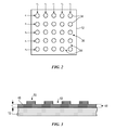
| US20070228589A1 (en) | 2002-11-13 | 2007-10-04 | Molecular Imprints, Inc. | Method for expelling gas positioned between a substrate and a mold |
| US20070228593A1 (en) | 2006-04-03 | 2007-10-04 | Molecular Imprints, Inc. | Residual Layer Thickness Measurement and Correction |
| US20070228610A1 (en) | 2006-04-03 | 2007-10-04 | Molecular Imprints, Inc. | Method of Concurrently Patterning a Substrate Having a Plurality of Fields and a Plurality of Alignment Marks |
| US20070231981A1 (en) | 2006-04-03 | 2007-10-04 | Molecular Imprints, Inc. | Patterning a Plurality of Fields on a Substrate to Compensate for Differing Evaporation Times |
| US20070228608A1 (en) | 2006-04-03 | 2007-10-04 | Molecular Imprints, Inc. | Preserving Filled Features when Vacuum Wiping |
| US7365103B2 (en) | 2002-12-12 | 2008-04-29 | Board Of Regents, The University Of Texas System | Compositions for dark-field polymerization and method of using the same for imprint lithography processes |
| US20080141862A1 (en) | 2003-10-02 | 2008-06-19 | Molecular Imprints, Inc. | Single Phase Fluid Imprint Lithography Method |
| JP4148549B2 (en) | 1997-12-02 | 2008-09-10 | 株式会社大宇エレクトロニクス | Mode signal encoding device |
| US7462028B2 (en) | 2006-04-03 | 2008-12-09 | Molecular Imprints, Inc. | Partial vacuum environment imprinting |
| US20080303187A1 (en) | 2006-12-29 | 2008-12-11 | Molecular Imprints, Inc. | Imprint Fluid Control |
Family Cites Families (119)
| Publication number | Priority date | Publication date | Assignee | Title |
|---|---|---|---|---|
| US3783520A (en) | 1970-09-28 | 1974-01-08 | Bell Telephone Labor Inc | High accuracy alignment procedure utilizing moire patterns |
| FR2325018A1 (en) | 1975-06-23 | 1977-04-15 | Ibm | INTERVAL MEASURING DEVICE FOR DEFINING THE DISTANCE BETWEEN TWO OR MORE FACES |
| GB1578259A (en) | 1977-05-11 | 1980-11-05 | Philips Electronic Associated | Methods of manufacturing solid-state devices apparatus for use therein and devices manufactured thereby |
| US4201800A (en) | 1978-04-28 | 1980-05-06 | International Business Machines Corp. | Hardened photoresist master image mask process |
| EP0091651B1 (en) | 1982-04-12 | 1988-08-03 | Nippon Telegraph And Telephone Corporation | Method for forming micropattern |
| FR2538923A1 (en) | 1982-12-30 | 1984-07-06 | Thomson Csf | METHOD AND DEVICE FOR OPTICALLY ALIGNING PATTERNS IN TWO PLANS RECONCILED IN AN EXPOSURE APPARATUS COMPRISING A DIVERGENT RADIATION SOURCE |
| US4507331A (en) | 1983-12-12 | 1985-03-26 | International Business Machines Corporation | Dry process for forming positive tone micro patterns |
| US4552833A (en) | 1984-05-14 | 1985-11-12 | International Business Machines Corporation | Radiation sensitive and oxygen plasma developable resist |
| US4908298A (en) | 1985-03-19 | 1990-03-13 | International Business Machines Corporation | Method of creating patterned multilayer films for use in production of semiconductor circuits and systems |
| EP0228671A1 (en) | 1985-12-23 | 1987-07-15 | General Electric Company | Method for the production of a coated substrate with controlled surface characteristics |
| US4657845A (en) | 1986-01-14 | 1987-04-14 | International Business Machines Corporation | Positive tone oxygen plasma developable photoresist |
| US4692205A (en) | 1986-01-31 | 1987-09-08 | International Business Machines Corporation | Silicon-containing polyimides as oxygen etch stop and dual dielectric coatings |
| US4737425A (en) | 1986-06-10 | 1988-04-12 | International Business Machines Corporation | Patterned resist and process |
| KR900004269B1 (en) | 1986-06-11 | 1990-06-18 | 가부시기가이샤 도시바 | Method and device for positioing 1st body and 2nd body |
| DE3760773D1 (en) | 1986-07-25 | 1989-11-16 | Oki Electric Ind Co Ltd | Negative resist material, method for its manufacture and method for using it |
| JPS6376330A (en) | 1986-09-18 | 1988-04-06 | Oki Electric Ind Co Ltd | Manufacture of semiconductor device |
| US4707218A (en) | 1986-10-28 | 1987-11-17 | International Business Machines Corporation | Lithographic image size reduction |
| US4931351A (en) | 1987-01-12 | 1990-06-05 | Eastman Kodak Company | Bilayer lithographic process |
| US6391798B1 (en) | 1987-02-27 | 2002-05-21 | Agere Systems Guardian Corp. | Process for planarization a semiconductor substrate |
| US5736424A (en) | 1987-02-27 | 1998-04-07 | Lucent Technologies Inc. | Device fabrication involving planarization |
| US4808511A (en) | 1987-05-19 | 1989-02-28 | International Business Machines Corporation | Vapor phase photoresist silylation process |
| US4936951A (en) | 1987-10-26 | 1990-06-26 | Matsushita Electric Industrial Co., Ltd. | Method of reducing proximity effect in electron beam resists |
| US4891303A (en) | 1988-05-26 | 1990-01-02 | Texas Instruments Incorporated | Trilayer microlithographic process using a silicon-based resist as the middle layer |
| JPH0224848A (en) | 1988-07-14 | 1990-01-26 | Canon Inc | Production of substrate for optical recording medium |
| JPH0269936A (en) | 1988-07-28 | 1990-03-08 | Siemens Ag | Method of making resin structure on semiconductor material |
| US4921778A (en) | 1988-07-29 | 1990-05-01 | Shipley Company Inc. | Photoresist pattern fabrication employing chemically amplified metalized material |
| US5108875A (en) | 1988-07-29 | 1992-04-28 | Shipley Company Inc. | Photoresist pattern fabrication employing chemically amplified metalized material |
| EP0355496A3 (en) | 1988-08-15 | 1990-10-10 | Sumitomo Heavy Industries Co., Ltd. | Position detector employing a sector fresnel zone plate |
| JP2546350B2 (en) | 1988-09-09 | 1996-10-23 | キヤノン株式会社 | Alignment device |
| JPH0292603A (en) | 1988-09-30 | 1990-04-03 | Hoya Corp | Manufacture of data recording board with guide groove |
| US4964945A (en) | 1988-12-09 | 1990-10-23 | Minnesota Mining And Manufacturing Company | Lift off patterning process on a flexible substrate |
| US5439766A (en) | 1988-12-30 | 1995-08-08 | International Business Machines Corporation | Composition for photo imaging |
| CA2010169A1 (en) | 1989-02-21 | 1990-08-21 | Masakazu Uekita | Multi-layer resist |
| US4999280A (en) | 1989-03-17 | 1991-03-12 | International Business Machines Corporation | Spray silylation of photoresist images |
| US5169494A (en) | 1989-03-27 | 1992-12-08 | Matsushita Electric Industrial Co., Ltd. | Fine pattern forming method |
| DE59010728D1 (en) | 1989-04-24 | 1997-07-31 | Siemens Ag | Process for producing etch-resistant structures |
| JP3001607B2 (en) | 1989-04-24 | 2000-01-24 | シーメンス、アクチエンゲゼルシヤフト | Dimensionally stable structure transfer method in two-layer method |
| US5110514A (en) * | 1989-05-01 | 1992-05-05 | Soane Technologies, Inc. | Controlled casting of a shrinkable material |
| US5053318A (en) | 1989-05-18 | 1991-10-01 | Shipley Company Inc. | Plasma processing with metal mask integration |
| CA2011927C (en) | 1989-06-02 | 1996-12-24 | Alan Lee Sidman | Microlithographic method for producing thick, vertically-walled photoresist patterns |
| US4919748A (en) | 1989-06-30 | 1990-04-24 | At&T Bell Laboratories | Method for tapered etching |
| JP2704001B2 (en) | 1989-07-18 | 1998-01-26 | キヤノン株式会社 | Position detection device |
| DE4031637C2 (en) | 1989-10-06 | 1997-04-10 | Toshiba Kawasaki Kk | Arrangement for measuring a displacement between two objects |
| US5362606A (en) | 1989-10-18 | 1994-11-08 | Massachusetts Institute Of Technology | Positive resist pattern formation through focused ion beam exposure and surface barrier silylation |
| US5139925A (en) | 1989-10-18 | 1992-08-18 | Massachusetts Institute Of Technology | Surface barrier silylation of novolak film without photoactive additive patterned with 193 nm excimer laser |
| JP3197010B2 (en) | 1990-03-05 | 2001-08-13 | 株式会社東芝 | Interval setting method and interval setting device |
| US5328810A (en) | 1990-05-07 | 1994-07-12 | Micron Technology, Inc. | Method for reducing, by a factor or 2-N, the minimum masking pitch of a photolithographic process |
| JP2524436B2 (en) | 1990-09-18 | 1996-08-14 | インターナショナル・ビジネス・マシーンズ・コーポレイション | Surface treatment method |
| DE4029912A1 (en) * | 1990-09-21 | 1992-03-26 | Philips Patentverwaltung | METHOD FOR FORMING AT LEAST ONE TRENCH IN A SUBSTRATE LAYER |
| US5314772A (en) | 1990-10-09 | 1994-05-24 | Arizona Board Of Regents | High resolution, multi-layer resist for microlithography and method therefor |
| US5240878A (en) | 1991-04-26 | 1993-08-31 | International Business Machines Corporation | Method for forming patterned films on a substrate |
| US5212147A (en) | 1991-05-15 | 1993-05-18 | Hewlett-Packard Company | Method of forming a patterned in-situ high Tc superconductive film |
| US5421981A (en) | 1991-06-26 | 1995-06-06 | Ppg Industries, Inc. | Electrochemical sensor storage device |
| EP0524759A1 (en) | 1991-07-23 | 1993-01-27 | AT&T Corp. | Device fabrication process |
| US5242711A (en) | 1991-08-16 | 1993-09-07 | Rockwell International Corp. | Nucleation control of diamond films by microlithographic patterning |
| US5263073A (en) | 1991-12-20 | 1993-11-16 | Board Of Supervisors Of Louisiana State University And Agricultural And Mechanical College | Scanning systems for high resolution E-beam and X-ray lithography |
| US5244818A (en) | 1992-04-08 | 1993-09-14 | Georgia Tech Research Corporation | Processes for lift-off of thin film materials and for the fabrication of three dimensional integrated circuits |
| US5376810A (en) | 1992-06-26 | 1994-12-27 | California Institute Of Technology | Growth of delta-doped layers on silicon CCD/S for enhanced ultraviolet response |
| US5431777A (en) | 1992-09-17 | 1995-07-11 | International Business Machines Corporation | Methods and compositions for the selective etching of silicon |
| TW227628B (en) | 1992-12-10 | 1994-08-01 | Samsung Electronics Co Ltd | |
| US5380474A (en) | 1993-05-20 | 1995-01-10 | Sandia Corporation | Methods for patterned deposition on a substrate |
| US5414514A (en) | 1993-06-01 | 1995-05-09 | Massachusetts Institute Of Technology | On-axis interferometric alignment of plates using the spatial phase of interference patterns |
| US5324683A (en) | 1993-06-02 | 1994-06-28 | Motorola, Inc. | Method of forming a semiconductor structure having an air region |
| JP2837063B2 (en) * | 1993-06-04 | 1998-12-14 | シャープ株式会社 | Method of forming resist pattern |
| US5900160A (en) * | 1993-10-04 | 1999-05-04 | President And Fellows Of Harvard College | Methods of etching articles via microcontact printing |
| KR970009858B1 (en) | 1994-01-12 | 1997-06-18 | 엘지반도체 주식회사 | Multi-layer photoresist patterning method |
| US5573877A (en) | 1994-03-15 | 1996-11-12 | Matsushita Electric Industrial Co., Ltd. | Exposure method and exposure apparatus |
| US5417802A (en) | 1994-03-18 | 1995-05-23 | At&T Corp. | Integrated circuit manufacturing |
| US5453157A (en) | 1994-05-16 | 1995-09-26 | Texas Instruments Incorporated | Low temperature anisotropic ashing of resist for semiconductor fabrication |
| US5670415A (en) | 1994-05-24 | 1997-09-23 | Depositech, Inc. | Method and apparatus for vacuum deposition of highly ionized media in an electromagnetic controlled environment |
| US5458520A (en) | 1994-12-13 | 1995-10-17 | International Business Machines Corporation | Method for producing planar field emission structure |
| US5743998A (en) | 1995-04-19 | 1998-04-28 | Park Scientific Instruments | Process for transferring microminiature patterns using spin-on glass resist media |
| US5948570A (en) | 1995-05-26 | 1999-09-07 | Lucent Technologies Inc. | Process for dry lithographic etching |
| US5808742A (en) | 1995-05-31 | 1998-09-15 | Massachusetts Institute Of Technology | Optical alignment apparatus having multiple parallel alignment marks |
| US5654238A (en) | 1995-08-03 | 1997-08-05 | International Business Machines Corporation | Method for etching vertical contact holes without substrate damage caused by directional etching |
| US6518168B1 (en) * | 1995-08-18 | 2003-02-11 | President And Fellows Of Harvard College | Self-assembled monolayer directed patterning of surfaces |
| US5900062A (en) * | 1995-12-28 | 1999-05-04 | Applied Materials, Inc. | Lift pin for dechucking substrates |
| US5802914A (en) | 1996-05-30 | 1998-09-08 | Eastman Kodak Company | Alignment mechanism using flexures |
| US6039897A (en) * | 1996-08-28 | 2000-03-21 | University Of Washington | Multiple patterned structures on a single substrate fabricated by elastomeric micro-molding techniques |
| US6228539B1 (en) * | 1996-09-18 | 2001-05-08 | Numerical Technologies, Inc. | Phase shifting circuit manufacture method and apparatus |
| US5895263A (en) | 1996-12-19 | 1999-04-20 | International Business Machines Corporation | Process for manufacture of integrated circuit device |
| US6049373A (en) | 1997-02-28 | 2000-04-11 | Sumitomo Heavy Industries, Ltd. | Position detection technique applied to proximity exposure |
| JP3296239B2 (en) | 1997-03-27 | 2002-06-24 | ウシオ電機株式会社 | Proximity exposure apparatus with gap setting mechanism |
| US5948219A (en) | 1997-05-07 | 1999-09-07 | Advanced Micro Devices, Inc. | Apparatus for selectively exposing a semiconductor topography to an electric field |
| US5926690A (en) | 1997-05-28 | 1999-07-20 | Advanced Micro Devices, Inc. | Run-to-run control process for controlling critical dimensions |
| US6033977A (en) | 1997-06-30 | 2000-03-07 | Siemens Aktiengesellschaft | Dual damascene structure |
| AU3818997A (en) | 1997-07-25 | 1999-02-16 | Regents Of The University Of Minnesota | Single-electron floating-gate mos memory |
| US6150680A (en) | 1998-03-05 | 2000-11-21 | Welch Allyn, Inc. | Field effect semiconductor device having dipole barrier |
| US6032997A (en) * | 1998-04-16 | 2000-03-07 | Excimer Laser Systems | Vacuum chuck |
| US6150231A (en) | 1998-06-15 | 2000-11-21 | Siemens Aktiengesellschaft | Overlay measurement technique using moire patterns |
| US5907782A (en) | 1998-08-15 | 1999-05-25 | Acer Semiconductor Manufacturing Inc. | Method of forming a multiple fin-pillar capacitor for a high density dram cell |
| US6096655A (en) | 1998-09-02 | 2000-08-01 | International Business Machines, Corporation | Method for forming vias and trenches in an insulation layer for a dual-damascene multilevel interconnection structure |
| AU1444800A (en) | 1998-10-09 | 2000-05-01 | Trustees Of Princeton University, The | Microscale patterning and articles formed thereby |
| JP4846888B2 (en) | 1998-12-01 | 2011-12-28 | キヤノン株式会社 | Alignment method |
| US6388755B1 (en) | 1998-12-03 | 2002-05-14 | Advanced Optical Technologies, Inc. | Wireless position and orientation detecting system |
| US6274294B1 (en) | 1999-02-03 | 2001-08-14 | Electroformed Stents, Inc. | Cylindrical photolithography exposure process and apparatus |
| US6387783B1 (en) | 1999-04-26 | 2002-05-14 | International Business Machines Corporation | Methods of T-gate fabrication using a hybrid resist |
| US6522411B1 (en) | 1999-05-25 | 2003-02-18 | Massachusetts Institute Of Technology | Optical gap measuring apparatus and method having two-dimensional grating mark with chirp in one direction |
| JP2001143982A (en) | 1999-06-29 | 2001-05-25 | Applied Materials Inc | Integrated dimension control for semiconductor device manufacturing |
| US6383928B1 (en) | 1999-09-02 | 2002-05-07 | Texas Instruments Incorporated | Post copper CMP clean |
| US6329256B1 (en) | 1999-09-24 | 2001-12-11 | Advanced Micro Devices, Inc. | Self-aligned damascene gate formation with low gate resistance |
| US6245581B1 (en) | 2000-04-19 | 2001-06-12 | Advanced Micro Devices, Inc. | Method and apparatus for control of critical dimension using feedback etch control |
| US6326627B1 (en) | 2000-08-02 | 2001-12-04 | Archimedes Technology Group, Inc. | Mass filtering sputtered ion source |
| US6451705B1 (en) | 2000-08-31 | 2002-09-17 | Micron Technology, Inc. | Self-aligned PECVD etch mask |
| US6455411B1 (en) | 2000-09-11 | 2002-09-24 | Texas Instruments Incorporated | Defect and etch rate control in trench etch for dual damascene patterning of low-k dielectrics |
| US6489068B1 (en) | 2001-02-21 | 2002-12-03 | Advanced Micro Devices, Inc. | Process for observing overlay errors on lithographic masks |
| US6955767B2 (en) * | 2001-03-22 | 2005-10-18 | Hewlett-Packard Development Company, Lp. | Scanning probe based lithographic alignment |
| US6791669B2 (en) | 2001-04-12 | 2004-09-14 | Nikon Corporation | Positioning device and exposure apparatus including the same |
| US6383888B1 (en) | 2001-04-18 | 2002-05-07 | Advanced Micro Devices, Inc. | Method and apparatus for selecting wafer alignment marks based on film thickness variation |
| US6678038B2 (en) * | 2001-08-03 | 2004-01-13 | Nikon Corporation | Apparatus and methods for detecting tool-induced shift in microlithography apparatus |
| EP1485944B1 (en) | 2002-03-15 | 2012-06-13 | Princeton University | Radiation assisted direct imprint lithography |
| JP4799861B2 (en) | 2002-04-16 | 2011-10-26 | プリンストン ユニバーシティ | Gradient structure for interface between microfluidic and nanofluid, and its manufacturing and use |
| JP2005527974A (en) | 2002-05-24 | 2005-09-15 | ワイ. チョウ,スティーヴン, | Method and apparatus for field induced pressure imprint lithography |
| US7027156B2 (en) | 2002-08-01 | 2006-04-11 | Molecular Imprints, Inc. | Scatterometry alignment for imprint lithography |
| AU2003300865A1 (en) | 2002-12-13 | 2004-07-09 | Molecular Imprints, Inc. | Magnification corrections employing out-of-plane distortions on a substrate |
| US6770852B1 (en) | 2003-02-27 | 2004-08-03 | Lam Research Corporation | Critical dimension variation compensation across a wafer by means of local wafer temperature control |
| WO2004114016A2 (en) | 2003-06-09 | 2004-12-29 | Princeton University Office Of Technology Licensing And Intellectual Property | Imprint lithography with improved monitoring and control and apparatus therefor |
| US7150622B2 (en) | 2003-07-09 | 2006-12-19 | Molecular Imprints, Inc. | Systems for magnification and distortion correction for imprint lithography processes |
| JP4090416B2 (en) * | 2003-09-30 | 2008-05-28 | 日東電工株式会社 | Separation method and separation device for workpiece with adhesive tape |
-
2002
- 2002-11-13 US US10/293,224 patent/US7019819B2/en not_active Expired - Lifetime
-
2003
- 2003-11-12 CN CN200380106274.9A patent/CN1726429B/en not_active Expired - Lifetime
-
2004
- 2004-06-09 US US10/864,591 patent/US6982783B2/en not_active Expired - Lifetime
-
2006
- 2006-03-27 US US11/389,731 patent/US7224443B2/en not_active Expired - Lifetime
- 2006-11-30 US US11/565,393 patent/US7691313B2/en not_active Expired - Lifetime
-
2010
- 2010-02-17 US US12/707,345 patent/US8282383B2/en not_active Expired - Lifetime
Patent Citations (218)
| Publication number | Priority date | Publication date | Assignee | Title |
|---|---|---|---|---|
| US3637381A (en) * | 1966-09-22 | 1972-01-25 | Teeg Research Inc | Radiation-sensitive self-revealing elements and methods of making and utilizing the same |
| US3997447A (en) | 1974-06-07 | 1976-12-14 | Composite Sciences, Inc. | Fluid processing apparatus |
| US4119688A (en) * | 1975-11-03 | 1978-10-10 | International Business Machines Corporation | Electro-lithography method |
| US4312823A (en) * | 1977-03-14 | 1982-01-26 | U.S. Philips Corporation | Method of manufacturing a plastic record carrier having a stratified structure |
| US4223261A (en) | 1978-08-23 | 1980-09-16 | Exxon Research & Engineering Co. | Multi-phase synchronous machine system |
| US4395211A (en) * | 1979-08-10 | 1983-07-26 | U.S. Philips Corporation | Method and device for manufacturing a plastic record carrier |
| US4279628A (en) | 1979-12-31 | 1981-07-21 | Energy Synergistics, Inc. | Apparatus for drying a natural gas stream |
| US4521175A (en) | 1980-03-14 | 1985-06-04 | Multivac Sepp Haggenmuller Kg | Apparatus for producing containers from thermoplastic sheet material |
| US4475223A (en) * | 1981-06-12 | 1984-10-02 | Hitachi, Ltd. | Exposure process and system |
| US4551192A (en) * | 1983-06-30 | 1985-11-05 | International Business Machines Corporation | Electrostatic or vacuum pinchuck formed with microcircuit lithography |
| US4506184A (en) * | 1984-01-10 | 1985-03-19 | Varian Associates, Inc. | Deformable chuck driven by piezoelectric means |
| US4512848A (en) | 1984-02-06 | 1985-04-23 | Exxon Research And Engineering Co. | Procedure for fabrication of microstructures over large areas using physical replication |
| US4559717A (en) | 1984-02-21 | 1985-12-24 | The United States Of America As Represented By The Secretary Of Commerce | Flexure hinge |
| US4767584A (en) | 1985-04-03 | 1988-08-30 | Massachusetts Institute Of Technology | Process of and apparatus for producing design patterns in materials |
| US4689004A (en) | 1985-04-18 | 1987-08-25 | Firma Carl Freudenberg | Apparatus for adhering thermally-softenable plastic particles into a plastic body |
| US4724222A (en) * | 1986-04-28 | 1988-02-09 | American Telephone And Telegraph Company, At&T Bell Laboratories | Wafer chuck comprising a curved reference surface |
| US4887282A (en) * | 1986-11-18 | 1989-12-12 | Siemens Aktiengesellschaft | Method and apparatus for changing the imaging scale in X-ray lithograph |
| US4731155A (en) | 1987-04-15 | 1988-03-15 | General Electric Company | Process for forming a lithographic mask |
| US5427599A (en) * | 1987-06-09 | 1995-06-27 | International Business Machines Corporation | System for stamping an optical storage disk |
| US5213600A (en) * | 1987-06-09 | 1993-05-25 | International Business Machines Corp. | Method of manufacturing an optical storage disk |
| US5132069A (en) | 1987-07-10 | 1992-07-21 | Newton John R | Method of injection molding composite articles |
| US5028361A (en) | 1987-11-09 | 1991-07-02 | Takeo Fujimoto | Method for molding a photosensitive composition |
| US5028366A (en) | 1988-01-12 | 1991-07-02 | Air Products And Chemicals, Inc. | Water based mold release compositions for making molded polyurethane foam |
| US5821175A (en) | 1988-07-08 | 1998-10-13 | Cauldron Limited Partnership | Removal of surface contaminants by irradiation using various methods to achieve desired inert gas flow over treated surface |
| US5527662A (en) * | 1990-05-24 | 1996-06-18 | Matsushita Electric Industrial Co., Ltd. | Process for forming fine pattern |
| US5331371A (en) | 1990-09-26 | 1994-07-19 | Canon Kabushiki Kaisha | Alignment and exposure method |
| US5324012A (en) | 1991-07-16 | 1994-06-28 | Nikon Corporation | Holding apparatus for holding an article such as a semiconductor wafer |
| US5259926A (en) | 1991-09-24 | 1993-11-09 | Hitachi, Ltd. | Method of manufacturing a thin-film pattern on a substrate |
| US5364222A (en) * | 1992-02-05 | 1994-11-15 | Tokyo Electron Limited | Apparatus for processing wafer-shaped substrates |
| US5545367A (en) | 1992-04-15 | 1996-08-13 | Soane Technologies, Inc. | Rapid prototype three dimensional stereolithography |
| US5338177A (en) | 1992-04-22 | 1994-08-16 | Societe Nationale Industrielle Et Aerospatiale | Hot compacting device for the production of parts requiring simultaneous pressure and temperature rises |
| US5601641A (en) | 1992-07-21 | 1997-02-11 | Tse Industries, Inc. | Mold release composition with polybutadiene and method of coating a mold core |
| US5534073A (en) * | 1992-09-07 | 1996-07-09 | Mitsubishi Denki Kabushiki Kaisha | Semiconductor producing apparatus comprising wafer vacuum chucking device |
| US5425848A (en) | 1993-03-16 | 1995-06-20 | U.S. Philips Corporation | Method of providing a patterned relief of cured photoresist on a flat substrate surface and device for carrying out such a method |
| US5550654A (en) * | 1993-07-19 | 1996-08-27 | Lucent Technologies Inc. | Method for forming, in optical media, refractive index perturbations having reduced birefringence |
| US5512131A (en) | 1993-10-04 | 1996-04-30 | President And Fellows Of Harvard College | Formation of microstamped patterns on surfaces and derivative articles |
| US6776094B1 (en) | 1993-10-04 | 2004-08-17 | President & Fellows Of Harvard College | Kit For Microcontact Printing |
| US5776748A (en) | 1993-10-04 | 1998-07-07 | President And Fellows Of Harvard College | Method of formation of microstamped patterns on plates for adhesion of cells and other biological materials, devices and uses therefor |
| US5515167A (en) | 1994-09-13 | 1996-05-07 | Hughes Aircraft Company | Transparent optical chuck incorporating optical monitoring |
| US5804089A (en) * | 1994-10-31 | 1998-09-08 | Matsushita Electric Industrial Co., Ltd. | Plasma processing apparatus and method |
| US5563684A (en) | 1994-11-30 | 1996-10-08 | Sgs-Thomson Microelectronics, Inc. | Adaptive wafer modulator for placing a selected pattern on a semiconductor wafer |
| US5849209A (en) | 1995-03-31 | 1998-12-15 | Johnson & Johnson Vision Products, Inc. | Mold material made with additives |
| US5956216A (en) | 1995-05-24 | 1999-09-21 | Regents Of The University Of Minnesota | Magnetic storage having discrete elements with quantized magnetic moments |
| US5820769A (en) | 1995-05-24 | 1998-10-13 | Regents Of The University Of Minnesota | Method for making magnetic storage having discrete elements with quantized magnetic moments |
| US6159400A (en) | 1995-08-01 | 2000-12-12 | Laquer; Henry Louis | Method for deforming solids in a controlled atmosphere and at adjustable rates, pressures and temperature |
| US5849222A (en) | 1995-09-29 | 1998-12-15 | Johnson & Johnson Vision Products, Inc. | Method for reducing lens hole defects in production of contact lens blanks |
| US6828244B2 (en) | 1995-11-15 | 2004-12-07 | Regents Of The University Of Minnesota | Method and apparatus for high density nanostructures |
| US20040137734A1 (en) | 1995-11-15 | 2004-07-15 | Princeton University | Compositions and processes for nanoimprinting |
| US5772905A (en) | 1995-11-15 | 1998-06-30 | Regents Of The University Of Minnesota | Nanoimprint lithography |
| US6518189B1 (en) | 1995-11-15 | 2003-02-11 | Regents Of The University Of Minnesota | Method and apparatus for high density nanostructures |
| US6809356B2 (en) | 1995-11-15 | 2004-10-26 | Regents Of The University Of Minnesota | Method and apparatus for high density nanostructures |
| US6309580B1 (en) | 1995-11-15 | 2001-10-30 | Regents Of The University Of Minnesota | Release surfaces, particularly for use in nanoimprint lithography |
| US5923408A (en) | 1996-01-31 | 1999-07-13 | Canon Kabushiki Kaisha | Substrate holding system and exposure apparatus using the same |
| US5669303A (en) * | 1996-03-04 | 1997-09-23 | Motorola | Apparatus and method for stamping a surface |
| US20020066978A1 (en) | 1996-03-15 | 2002-06-06 | Enoch Kim | Method of forming articles including waveguides via capillary micromolding and microtransfer molding |
| US6355198B1 (en) | 1996-03-15 | 2002-03-12 | President And Fellows Of Harvard College | Method of forming articles including waveguides via capillary micromolding and microtransfer molding |
| US20030179354A1 (en) | 1996-03-22 | 2003-09-25 | Nikon Corporation | Mask-holding apparatus for a light exposure apparatus and related scanning-exposure method |
| US6032506A (en) * | 1996-05-30 | 2000-03-07 | S.C. Recherche Et Developpement Groupe | Improvment to the blank holder force regulating system in a press |
| US6257866B1 (en) | 1996-06-18 | 2001-07-10 | Hy-Tech Forming Systems, Inc. | Apparatus for accurately forming plastic sheet |
| US6137562A (en) * | 1996-12-05 | 2000-10-24 | Nikon Corporation | Substrate adjuster, substrate holder and substrate holding method |
| US5948470A (en) | 1997-04-28 | 1999-09-07 | Harrison; Christopher | Method of nanoscale patterning and products made thereby |
| US6182510B1 (en) | 1997-04-30 | 2001-02-06 | Sensys Instruments Corporation | Apparatus and method for characterizing semiconductor wafers during processing |
| JP4148549B2 (en) | 1997-12-02 | 2008-09-10 | 株式会社大宇エレクトロニクス | Mode signal encoding device |
| US6383890B2 (en) * | 1997-12-26 | 2002-05-07 | Canon Kabushiki Kaisha | Wafer bonding method, apparatus and vacuum chuck |
| US6019166A (en) | 1997-12-30 | 2000-02-01 | Intel Corporation | Pickup chuck with an integral heatsink |
| US6030275A (en) * | 1998-03-17 | 2000-02-29 | International Business Machines Corporation | Variable control of carrier curvature with direct feedback loop |
| US6416311B1 (en) | 1998-05-04 | 2002-07-09 | Jenoptik Aktiengesellschaft | Device and method for separating a shaped substrate from a stamping tool |
| US5997963A (en) | 1998-05-05 | 1999-12-07 | Ultratech Stepper, Inc. | Microchamber |
| US6646662B1 (en) | 1998-05-26 | 2003-11-11 | Seiko Epson Corporation | Patterning method, patterning apparatus, patterning template, and method for manufacturing the patterning template |
| US20030034329A1 (en) | 1998-06-30 | 2003-02-20 | Chou Stephen Y. | Lithographic method for molding pattern with nanoscale depth |
| US20020167117A1 (en) | 1998-06-30 | 2002-11-14 | Regents Of The University Of Minnesota | Release surfaces, particularly for use in nanoimprint lithography |
| US6099771A (en) | 1998-07-08 | 2000-08-08 | Lear Corporation | Vacuum compression method for forming molded thermoplastic floor mat having a "Class A" finish |
| US5947027A (en) * | 1998-09-08 | 1999-09-07 | Motorola, Inc. | Printing apparatus with inflatable means for advancing a substrate towards the stamping surface |
| US20020042027A1 (en) | 1998-10-09 | 2002-04-11 | Chou Stephen Y. | Microscale patterning and articles formed thereby |
| US6713238B1 (en) | 1998-10-09 | 2004-03-30 | Stephen Y. Chou | Microscale patterning and articles formed thereby |
| US20040118809A1 (en) | 1998-10-09 | 2004-06-24 | Chou Stephen Y. | Microscale patterning and articles formed thereby |
| US6726195B1 (en) | 1998-10-13 | 2004-04-27 | Dek International Gmbh | Method for ensuring planarity when using a flexible, self conforming, workpiece support system |
| US6218316B1 (en) | 1998-10-22 | 2001-04-17 | Micron Technology, Inc. | Planarization of non-planar surfaces in device fabrication |
| US6247579B1 (en) | 1999-01-18 | 2001-06-19 | Tokyo Ohka Kogyo Co., Ltd | Substrate transfer apparatus and method of substrate transfer |
| US6334960B1 (en) | 1999-03-11 | 2002-01-01 | Board Of Regents, The University Of Texas System | Step and flash imprint lithography |
| US20050236739A1 (en) | 1999-03-11 | 2005-10-27 | Board Of Regents, The University Of Texas System | Step and flash imprint lithography |
| US6160430A (en) | 1999-03-22 | 2000-12-12 | Ati International Srl | Powerup sequence artificial voltage supply circuit |
| US6305677B1 (en) | 1999-03-30 | 2001-10-23 | Lam Research Corporation | Perimeter wafer lifting |
| US6461524B1 (en) | 1999-05-27 | 2002-10-08 | Sanyo Electric Co., Ltd. | Method of filtering a fluid |
| US6220561B1 (en) | 1999-06-30 | 2001-04-24 | Sandia Corporation | Compound floating pivot micromechanisms |
| EP1072954A2 (en) | 1999-07-28 | 2001-01-31 | Lucent Technologies Inc. | Lithographic process for device fabrication |
| US6809802B1 (en) * | 1999-08-19 | 2004-10-26 | Canon Kabushiki Kaisha | Substrate attracting and holding system for use in exposure apparatus |
| US20040036850A1 (en) | 1999-08-19 | 2004-02-26 | Canon Kabushiki Kaisha | Substrate attracting and holding system for use in exposure apparatus |
| US6407006B1 (en) | 1999-09-09 | 2002-06-18 | Honeywell International, Inc. | Method for integrated circuit planarization |
| US6512401B2 (en) | 1999-09-10 | 2003-01-28 | Intel Corporation | Output buffer for high and low voltage bus |
| US6517995B1 (en) | 1999-09-14 | 2003-02-11 | Massachusetts Institute Of Technology | Fabrication of finely featured devices by liquid embossing |
| US20040104641A1 (en) * | 1999-10-29 | 2004-06-03 | University Of Texas System | Method of separating a template from a substrate during imprint lithography |
| US6873087B1 (en) | 1999-10-29 | 2005-03-29 | Board Of Regents, The University Of Texas System | High precision orientation alignment and gap control stages for imprint lithography processes |
| WO2001040875A1 (en) | 1999-11-30 | 2001-06-07 | Silicon Valley Group, Inc. | Dual-stage lithography apparatus and method |
| US6391217B2 (en) | 1999-12-23 | 2002-05-21 | University Of Massachusetts | Methods and apparatus for forming submicron patterns on films |
| US6869980B2 (en) | 2000-03-02 | 2005-03-22 | Celanese Ventures Gmbh | Polymer blend membranes for use in fuel cells |
| US6313567B1 (en) | 2000-04-10 | 2001-11-06 | Motorola, Inc. | Lithography chuck having piezoelectric elements, and method |
| US20020018190A1 (en) | 2000-06-15 | 2002-02-14 | Hideki Nogawa | Exposure apparatus and device manufacturing method |
| US20040141163A1 (en) | 2000-07-16 | 2004-07-22 | The University Of Texas System, Board Of Regents, Ut System | Device for holding a template for use in imprint lithography |
| US6916585B2 (en) | 2000-07-16 | 2005-07-12 | Board Of Regents, The University Of Texas Systems | Method of varying template dimensions to achieve alignment during imprint lithography |
| US6842229B2 (en) | 2000-07-16 | 2005-01-11 | Board Of Regents, The University Of Texas System | Imprint lithography template comprising alignment marks |
| US20040163563A1 (en) | 2000-07-16 | 2004-08-26 | The Board Of Regents, The University Of Texas System | Imprint lithography template having a mold to compensate for material changes of an underlying liquid |
| US20080199816A1 (en) | 2000-07-17 | 2008-08-21 | The University Of Texas Board Of Regents | Method of Automatic Fluid Dispensing for Imprint Lithography Processes |
| US20020094496A1 (en) * | 2000-07-17 | 2002-07-18 | Choi Byung J. | Method and system of automatic fluid dispensing for imprint lithography processes |
| US20050037143A1 (en) | 2000-07-18 | 2005-02-17 | Chou Stephen Y. | Imprint lithography with improved monitoring and control and apparatus therefor |
| US20040131718A1 (en) | 2000-07-18 | 2004-07-08 | Princeton University | Lithographic apparatus for fluid pressure imprint lithography |
| US20040036201A1 (en) | 2000-07-18 | 2004-02-26 | Princeton University | Methods and apparatus of field-induced pressure imprint lithography |
| US20020177319A1 (en) | 2000-07-18 | 2002-11-28 | Chou Stephen Y. | Fluid pressure bonding |
| US20040046288A1 (en) | 2000-07-18 | 2004-03-11 | Chou Stephen Y. | Laset assisted direct imprint lithography |
| US6482742B1 (en) | 2000-07-18 | 2002-11-19 | Stephen Y. Chou | Fluid pressure imprint lithography |
| US20020132482A1 (en) | 2000-07-18 | 2002-09-19 | Chou Stephen Y. | Fluid pressure imprint lithography |
| US6954275B2 (en) * | 2000-08-01 | 2005-10-11 | Boards Of Regents, The University Of Texas System | Methods for high-precision gap and orientation sensing between a transparent template and substrate for imprint lithography |
| US20020150398A1 (en) | 2000-08-21 | 2002-10-17 | Choi Byung J. | Flexure based macro motion translation stage |
| US20020069525A1 (en) | 2000-09-18 | 2002-06-13 | Junichi Hada | Apparatus and method for mounting components on substrate |
| US7060324B2 (en) | 2000-10-12 | 2006-06-13 | Board Of Regents, The University Of Texas System | Method of creating a dispersion of a liquid on a substrate |
| US6696220B2 (en) * | 2000-10-12 | 2004-02-24 | Board Of Regents, The University Of Texas System | Template for room temperature, low pressure micro-and nano-imprint lithography |
| US20030092261A1 (en) * | 2000-12-04 | 2003-05-15 | Fumio Kondo | Substrate processing method |
| US6612590B2 (en) | 2001-01-12 | 2003-09-02 | Tokyo Electron Limited | Apparatus and methods for manipulating semiconductor wafers |
| US6580172B2 (en) | 2001-03-02 | 2003-06-17 | Motorola, Inc. | Lithographic template and method of formation and use |
| US7018572B2 (en) * | 2001-06-11 | 2006-03-28 | General Electric Company | Method for producing data storage media |
| US20040197843A1 (en) | 2001-07-25 | 2004-10-07 | Chou Stephen Y. | Nanochannel arrays and their preparation and use for high throughput macromolecular analysis |
| US20030062334A1 (en) | 2001-09-25 | 2003-04-03 | Lee Hong Hie | Method for forming a micro-pattern on a substrate by using capillary force |
| US20040156108A1 (en) | 2001-10-29 | 2004-08-12 | Chou Stephen Y. | Articles comprising nanoscale patterns with reduced edge roughness and methods of making same |
| US20030080471A1 (en) | 2001-10-29 | 2003-05-01 | Chou Stephen Y. | Lithographic method for molding pattern with nanoscale features |
| US20030080472A1 (en) | 2001-10-29 | 2003-05-01 | Chou Stephen Y. | Lithographic method with bonded release layer for molding small patterns |
| US6771372B1 (en) | 2001-11-01 | 2004-08-03 | Therma-Wave, Inc. | Rotational stage with vertical axis adjustment |
| US6764386B2 (en) | 2002-01-11 | 2004-07-20 | Applied Materials, Inc. | Air bearing-sealed micro-processing chamber |
| US6736408B2 (en) | 2002-01-25 | 2004-05-18 | Applied Materials Inc. | Rotary vacuum-chuck with venturi formed at base of rotating shaft |
| US20040029041A1 (en) * | 2002-02-27 | 2004-02-12 | Brewer Science, Inc. | Novel planarization method for multi-layer lithography processing |
| US20030189273A1 (en) | 2002-04-04 | 2003-10-09 | Lennart Olsson | Imprint method and device |
| US7144539B2 (en) * | 2002-04-04 | 2006-12-05 | Obducat Ab | Imprint method and device |
| US6849558B2 (en) | 2002-05-22 | 2005-02-01 | The Board Of Trustees Of The Leland Stanford Junior University | Replication and transfer of microstructures and nanostructures |
| US20030235787A1 (en) | 2002-06-24 | 2003-12-25 | Watts Michael P.C. | Low viscosity high resolution patterning material |
| US6926929B2 (en) | 2002-07-09 | 2005-08-09 | Molecular Imprints, Inc. | System and method for dispensing liquids |
| US7252715B2 (en) | 2002-07-09 | 2007-08-07 | Molecular Imprints, Inc. | System for dispensing liquids |
| US6908861B2 (en) | 2002-07-11 | 2005-06-21 | Molecular Imprints, Inc. | Method for imprint lithography using an electric field |
| US20040009673A1 (en) * | 2002-07-11 | 2004-01-15 | Sreenivasan Sidlgata V. | Method and system for imprint lithography using an electric field |
| US20060077374A1 (en) | 2002-07-11 | 2006-04-13 | Molecular Imprints, Inc. | Step and repeat imprint lithography systems |
| US7338275B2 (en) | 2002-07-11 | 2008-03-04 | Molecular Imprints, Inc. | Formation of discontinuous films during an imprint lithography process |
| US20040124566A1 (en) * | 2002-07-11 | 2004-07-01 | Sreenivasan Sidlgata V. | Step and repeat imprint lithography processes |
| US20060076717A1 (en) | 2002-07-11 | 2006-04-13 | Molecular Imprints, Inc. | Step and repeat imprint lithography processes |
| US6932934B2 (en) | 2002-07-11 | 2005-08-23 | Molecular Imprints, Inc. | Formation of discontinuous films during an imprint lithography process |
| US7077992B2 (en) | 2002-07-11 | 2006-07-18 | Molecular Imprints, Inc. | Step and repeat imprint lithography processes |
| US6900881B2 (en) | 2002-07-11 | 2005-05-31 | Molecular Imprints, Inc. | Step and repeat imprint lithography systems |
| US20060062867A1 (en) | 2002-07-11 | 2006-03-23 | Molecular Imprints, Inc. | Formation of discontinuous films during an imprint lithography process |
| US6916584B2 (en) | 2002-08-01 | 2005-07-12 | Molecular Imprints, Inc. | Alignment methods for imprint lithography |
| US20040022888A1 (en) * | 2002-08-01 | 2004-02-05 | Sreenivasan Sidlgata V. | Alignment systems for imprint lithography |
| US7071088B2 (en) | 2002-08-23 | 2006-07-04 | Molecular Imprints, Inc. | Method for fabricating bulbous-shaped vias |
| US20040132301A1 (en) | 2002-09-12 | 2004-07-08 | Harper Bruce M. | Indirect fluid pressure imprinting |
| US20040065976A1 (en) | 2002-10-04 | 2004-04-08 | Sreenivasan Sidlgata V. | Method and a mold to arrange features on a substrate to replicate features having minimal dimensional variability |
| US6982783B2 (en) | 2002-11-13 | 2006-01-03 | Molecular Imprints, Inc. | Chucking system for modulating shapes of substrates |
| US20070228589A1 (en) | 2002-11-13 | 2007-10-04 | Molecular Imprints, Inc. | Method for expelling gas positioned between a substrate and a mold |
| US6929762B2 (en) | 2002-11-13 | 2005-08-16 | Molecular Imprints, Inc. | Method of reducing pattern distortions during imprint lithography processes |
| US7019819B2 (en) | 2002-11-13 | 2006-03-28 | Molecular Imprints, Inc. | Chucking system for modulating shapes of substrates |
| WO2004044651B1 (en) | 2002-11-13 | 2004-08-05 | Molecular Imprints Inc | A chucking system and method for modulating shapes of substrates |
| US7224443B2 (en) | 2002-11-13 | 2007-05-29 | Molecular Imprints, Inc. | Imprint lithography substrate processing tool for modulating shapes of substrates |
| US20040110856A1 (en) | 2002-12-04 | 2004-06-10 | Young Jung Gun | Polymer solution for nanoimprint lithography to reduce imprint temperature and pressure |
| US6980282B2 (en) | 2002-12-11 | 2005-12-27 | Molecular Imprints, Inc. | Method for modulating shapes of substrates |
| US7036389B2 (en) | 2002-12-12 | 2006-05-02 | Molecular Imprints, Inc. | System for determining characteristics of substrates employing fluid geometries |
| US6871558B2 (en) | 2002-12-12 | 2005-03-29 | Molecular Imprints, Inc. | Method for determining characteristics of substrate employing fluid geometries |
| US6990870B2 (en) | 2002-12-12 | 2006-01-31 | Molecular Imprints, Inc. | System for determining characteristics of substrates employing fluid geometries |
| US7365103B2 (en) | 2002-12-12 | 2008-04-29 | Board Of Regents, The University Of Texas System | Compositions for dark-field polymerization and method of using the same for imprint lithography processes |
| US20040129293A1 (en) | 2003-01-08 | 2004-07-08 | Eichenberger Louis C. | Flow system flush process |
| US20040170770A1 (en) | 2003-02-27 | 2004-09-02 | Molecular Imprints, Inc. | Method to reduce adhesion between a polymerizable layer and a substrate employing a fluorine-containing layer |
| US20040168613A1 (en) | 2003-02-27 | 2004-09-02 | Molecular Imprints, Inc. | Composition and method to form a release layer |
| US20040192041A1 (en) | 2003-03-27 | 2004-09-30 | Jun-Ho Jeong | UV nanoimprint lithography process using elementwise embossed stamp and selectively additive pressurization |
| US20040250945A1 (en) | 2003-06-10 | 2004-12-16 | Industrial Technology Research Institute | Method for and apparatus for bonding patterned imprint to a substrate by adhering means |
| US20050024609A1 (en) | 2003-06-11 | 2005-02-03 | Asml Netherlands B.V. | Lithographic apparatus and device manufacturing method |
| US20050061773A1 (en) | 2003-08-21 | 2005-03-24 | Byung-Jin Choi | Capillary imprinting technique |
| WO2005019934A3 (en) | 2003-08-22 | 2005-06-02 | 3M Innovative Properties Co | Precursor paste and method of producing the same |
| US20050046449A1 (en) | 2003-08-26 | 2005-03-03 | Davis Jeffrey B. | Voltage mismatch tolerant input/output buffer |
| US7090716B2 (en) | 2003-10-02 | 2006-08-15 | Molecular Imprints, Inc. | Single phase fluid imprint lithography method |
| US20050074512A1 (en) | 2003-10-02 | 2005-04-07 | University Of Texas System Board Of Regents | System for creating a turbulent flow of fluid between a mold and a substrate |
| US20050072757A1 (en) | 2003-10-02 | 2005-04-07 | University Of Texas System Board Of Regents | Method of creating a turbulent flow of fluid between a mold and a substrate |
| US20080141862A1 (en) | 2003-10-02 | 2008-06-19 | Molecular Imprints, Inc. | Single Phase Fluid Imprint Lithography Method |
| US7270533B2 (en) | 2003-10-02 | 2007-09-18 | University Of Texas System, Board Of Regents | System for creating a turbulent flow of fluid between a mold and a substrate |
| US7531025B2 (en) | 2003-10-02 | 2009-05-12 | Molecular Imprints, Inc. | Method of creating a turbulent flow of fluid between a mold and a substrate |
| US20050106321A1 (en) | 2003-11-14 | 2005-05-19 | Molecular Imprints, Inc. | Dispense geometery to achieve high-speed filling and throughput |
| US7023238B1 (en) | 2004-01-07 | 2006-04-04 | Altera Corporation | Input buffer with selectable threshold and hysteresis option |
| US20050156353A1 (en) | 2004-01-15 | 2005-07-21 | Watts Michael P. | Method to improve the flow rate of imprinting material |
| US20060125154A1 (en) | 2004-01-15 | 2006-06-15 | Molecular Imprints, Inc. | Method to improve the flow rate of imprinting material employing an absorption layer |
| US20050158419A1 (en) | 2004-01-15 | 2005-07-21 | Watts Michael P. | Thermal processing system for imprint lithography |
| US20050187339A1 (en) | 2004-02-23 | 2005-08-25 | Molecular Imprints, Inc. | Materials for imprint lithography |
| US20050189676A1 (en) | 2004-02-27 | 2005-09-01 | Molecular Imprints, Inc. | Full-wafer or large area imprinting with multiple separated sub-fields for high throughput lithography |
| US20050274693A1 (en) * | 2004-05-07 | 2005-12-15 | Babak Heidari | Device and method for lithography |
| US20050263249A1 (en) | 2004-05-28 | 2005-12-01 | Board Of Regents, The University Of Texas System | Substrate support system |
| US20050264134A1 (en) | 2004-05-28 | 2005-12-01 | Board Of Regents, The University Of Texas System | Adaptive shape substrate support system |
| US7245358B2 (en) | 2004-05-28 | 2007-07-17 | Board Of Regents, The University Of Texas System | Substrate support system |
| US20050276919A1 (en) | 2004-06-01 | 2005-12-15 | Molecular Imprints, Inc. | Method for dispensing a fluid on a substrate |
| US20050270516A1 (en) | 2004-06-03 | 2005-12-08 | Molecular Imprints, Inc. | System for magnification and distortion correction during nano-scale manufacturing |
| US20050270312A1 (en) | 2004-06-03 | 2005-12-08 | Molecular Imprints, Inc. | Fluid dispensing and drop-on-demand dispensing for nano-scale manufacturing |
| US7298456B2 (en) | 2004-06-03 | 2007-11-20 | Molecular Imprints, Inc. | System for varying dimensions of a substrate during nanoscale manufacturing |
| US20060063112A1 (en) | 2004-09-21 | 2006-03-23 | Molecular Imprints, Inc. | Pattern reversal employing thick residual layers |
| US20060062922A1 (en) | 2004-09-23 | 2006-03-23 | Molecular Imprints, Inc. | Polymerization technique to attenuate oxygen inhibition of solidification of liquids and composition therefor |
| US20070141271A1 (en) | 2004-09-23 | 2007-06-21 | Molecular Imprints, Inc. | Method for controlling distribution of fluid components on a body |
| US7244386B2 (en) | 2004-09-27 | 2007-07-17 | Molecular Imprints, Inc. | Method of compensating for a volumetric shrinkage of a material disposed upon a substrate to form a substantially planar structure therefrom |
| US20060115999A1 (en) | 2004-12-01 | 2006-06-01 | Molecular Imprints, Inc. | Methods of exposure for the purpose of thermal management for imprint lithography processes |
| US20060121728A1 (en) | 2004-12-07 | 2006-06-08 | Molecular Imprints, Inc. | Method for fast filling of templates for imprint lithography using on template dispense |
| US7281919B2 (en) | 2004-12-07 | 2007-10-16 | Molecular Imprints, Inc. | System for controlling a volume of material on a mold |
| US7473090B2 (en) | 2005-01-31 | 2009-01-06 | Molecular Imprints, Inc. | Imprint lithography template to facilitate control of liquid movement |
| US20060172031A1 (en) | 2005-01-31 | 2006-08-03 | Molecular Imprints, Inc. | Chucking system for nano-manufacturing |
| US20060177532A1 (en) | 2005-02-04 | 2006-08-10 | Molecular Imprints, Inc. | Imprint lithography method to control extrusion of a liquid from a desired region on a substrate |
| US20060177535A1 (en) | 2005-02-04 | 2006-08-10 | Molecular Imprints, Inc. | Imprint lithography template to facilitate control of liquid movement |
| US20060268256A1 (en) | 2005-05-27 | 2006-11-30 | Asml Netherlands B.V. | Imprint lithography |
| US7316554B2 (en) | 2005-09-21 | 2008-01-08 | Molecular Imprints, Inc. | System to control an atmosphere between a body and a substrate |
| US20070065532A1 (en) | 2005-09-21 | 2007-03-22 | Molecular Imprints, Inc. | System to control an atmosphere between a body and a substrate |
| US20070063384A1 (en) | 2005-09-21 | 2007-03-22 | Molecular Imprints, Inc. | Method to control an atmostphere between a body and a substrate |
| US20070077763A1 (en) | 2005-09-30 | 2007-04-05 | Molecular Imprints, Inc. | Deposition technique to planarize a multi-layer structure |
| US7259102B2 (en) | 2005-09-30 | 2007-08-21 | Molecular Imprints, Inc. | Etching technique to planarize a multi-layer structure |
| US20070126150A1 (en) | 2005-12-01 | 2007-06-07 | Molecular Imprints, Inc. | Bifurcated contact printing technique |
| US20070132152A1 (en) | 2005-12-08 | 2007-06-14 | Molecular Imprints, Inc. | Method and System for Double-Sided Patterning of Substrates |
| US20070170617A1 (en) | 2006-01-20 | 2007-07-26 | Molecular Imprints, Inc. | Patterning Substrates Employing Multiple Chucks |
| US20070228608A1 (en) | 2006-04-03 | 2007-10-04 | Molecular Imprints, Inc. | Preserving Filled Features when Vacuum Wiping |
| US20070231981A1 (en) | 2006-04-03 | 2007-10-04 | Molecular Imprints, Inc. | Patterning a Plurality of Fields on a Substrate to Compensate for Differing Evaporation Times |
| US20070228610A1 (en) | 2006-04-03 | 2007-10-04 | Molecular Imprints, Inc. | Method of Concurrently Patterning a Substrate Having a Plurality of Fields and a Plurality of Alignment Marks |
| US20070228593A1 (en) | 2006-04-03 | 2007-10-04 | Molecular Imprints, Inc. | Residual Layer Thickness Measurement and Correction |
| US7462028B2 (en) | 2006-04-03 | 2008-12-09 | Molecular Imprints, Inc. | Partial vacuum environment imprinting |
| US20080303187A1 (en) | 2006-12-29 | 2008-12-11 | Molecular Imprints, Inc. | Imprint Fluid Control |
Non-Patent Citations (38)
| Title |
|---|
| Abstract of Japanese Patent 02-24848, Jan. 26, 1990. |
| Abstract of Japanese Patent 02-92603, Aug. 12, 2004. |
| Abstract of Japanese Patent 4-148549 (1992). |
| Abstract of Japanese Patent 57-032629 (1982 ). |
| Abstract of Japanese Patent 57-153434 (1982). |
| Abstract of Japanese Patent 60-127935 (1985). |
| Bailey et al., Step and Flash Imprint Lithography: Defect Analysis, Journal of Vacuum Science, B 19(6), pp. 2806-2810 Nov. 1, 2001. |
| Bailey et al., Step and Flash Imprint Lithography: Template Surface Treatment and Defect Analysis, Journal of Vacuum Science, B 18(6), pp. 3572-3577 Nov. 1, 2000. |
| Choi et al., Design of Orientation Stages for Step and Flash Imprint Lithography, Precision Engineering, pp. 192-199 Jan. 1, 2001. |
| Chou et al., Imprint Lithography with 25-Nanometer Resolution, Science vol. 272, pp. 85-87 Apr. 5, 1996. |
| Chou et al., Imprint Lithography with Sub-10 nm Feature Size and High Throughput, Microelectronic Engineering 35, pp. 237-240 Jan. 1, 1997. |
| Chou et al., Imprint of Sub-25 nm Vias and Trenches in Polymers, Appl. Phys. Lett. 67 (21) Nov. 20, 1995. |
| Chou et al., Lithographically Induced Self-assembly of Periodic Polymer Micropillar Arrays, J. Vac. Sci. Technol. B 17 (6), pp. 3197-3202 Nov. 1, 1999. |
| Chou et al., Nanoimprint Lithography, Journal of Vacuum Science Technolgoy B 14(16), pp. 4129-4133 Nov. 1, 1996. |
| Chou et al., Ultrafast and Direct Imprint of Nanostructures in Silicon, Nature, col. 417, (Jun. 2002), pp. 835-837 Jun. 1, 2002. |
| Chou, Nanoimprint Lithography and Lithographically Induced Self-Assembly, MRS Bulletin, pp. 512-517 Jul. 1, 2001. |
| Colburn et al., Characterization and Modeling of Volumetric and Mechanical Properties for Step and Flash Imprint Lithography Photopolymers, Journal of Vacuum Science Technology. vol b. 19(6) Nov. 1, 2001. |
| Colburn et al., Development and Advantages of Step-and-Flash Lithography, Solid State Technology Jul. 1, 2001. |
| Colburn et al., Dissertation for the Degree of Doctor of Philosophy, Step and Flash Imprint Lithography: A Low-Pressure, Room-Temperature Nanoimprint Lithography Aug. 1, 2001. |
| Colburn et al., Step and Flash Imprint Lithography for sub-100 nm Patterning, Proceedings of SPIE vol. 3997, pp. 453-457 Jan. 1, 2000. |
| Colburn et al., Step and Flash Imprint Lithography: A New Approach to High-Resolution Patterning, Proc. Of SPIE, vol. 3676 Mar. 1, 1999. |
| Feldman, Wafer Chuck for Magnification Correction in X-ray Lithography, J. Vac. Sci. Technol. B 16(6), pp. 3476-3479 Nov. 1, 1998. |
| Feynman, There's Plenty of Room at the Bottom, Dec. 1, 1959. |
| Final Office Action in U.S. Appl. No. 12/026,049, filed May 29, 2009. |
| Haisma et al., Mold-assisted Nanolithography: A Process for Reliable Pattern Replication, J. Vac. Sci. Technol. B, pp. 4124-4128 Nov. 1, 1996. |
| Heidari, Nanoimprint Lithography at the 6 in. Wafer Scale, J. Vac. Sci. Technol. B 18(6), pp. 3557-3560 Nov. 1, 2000. |
| Johnson et al., Advances in Step and Flash Imprint Lithography, SPIE Microlithography Conference Feb. 23, 2003. |
| Michel et al., Printing Meets Lithography: Soft Approaches for High-Resolution Patterning, IBM Journal of Research and Development, International Business Machines Corporation, New York, NY, US, vol. 45, No. 5, pp. 697-719 Sep. 1, 2001. |
| Nguyen, Asymmetric Fluid-Structure Dynamics in Nanoscale Imprint Lithography, The University of Texas at Austin, pp. 1-111 Aug. 1, 2001. |
| Non-Final Office Action in U.S. Appl. No. 12/026,049, filed Oct. 8, 2008. |
| PCT/US07/12071 ISR, Jul. 2, 2008. |
| Schneider et al., Stripes of Partially Fluorinated Alkyl Chains: Dipolar Langmuir Monolayers, J. Chem. Phys. vol. 122, Issue 9 Mar. 1, 2005. |
| Translation of Japanese Patent 02-24848, Jan. 26, 1990. |
| Translation of Japanese Patent 02-92603, Apr. 3, 1990. |
| U.S. Appl. No. 11/690,480, naming Inventors Cherala et al., entitled Chucking System Comprising an Array of Fluid Chambers, filed Mar. 23, 2007. |
| U.S. Appl. No. 11/695,263, naming Inventors Cherala et al., entitled Partial Vacuum Environment Imprinting, filed Apr. 2, 2007. |
| U.S. Appl. No. 11/749,909, naming Inventors Choi et al., entitled Method for Expelling Gas Positioned Between a Substrate and a Mold, filed May 17, 2007. |
| Xia et al., Soft Lithography, Angew. Chem. Int. Ed., pp. 550-575 Jan. 1, 1998. |
Cited By (44)
| Publication number | Priority date | Publication date | Assignee | Title |
|---|---|---|---|---|
| US8556616B2 (en) | 2002-07-08 | 2013-10-15 | Molecular Imprints, Inc. | Template having a varying thickness to facilitate expelling a gas positioned between a substrate and the template |
| US20110171340A1 (en) * | 2002-07-08 | 2011-07-14 | Molecular Imprints, Inc. | Template Having a Varying Thickness to Facilitate Expelling a Gas Positioned Between a Substrate and the Template |
| US20050270312A1 (en) * | 2004-06-03 | 2005-12-08 | Molecular Imprints, Inc. | Fluid dispensing and drop-on-demand dispensing for nano-scale manufacturing |
| US20080202365A1 (en) * | 2005-05-03 | 2008-08-28 | Koninklijke Philips Electronics, N.V. | Method and Device For Transferring a Pattern From a Stamp to a Substrate |
| US8166876B2 (en) * | 2005-05-03 | 2012-05-01 | Koninklijke Philips Electronics N.V. | Method and device for transferring a pattern from a stamp to a substrate |
| USRE47483E1 (en) | 2006-05-11 | 2019-07-02 | Molecular Imprints, Inc. | Template having a varying thickness to facilitate expelling a gas positioned between a substrate and the template |
| US9440254B2 (en) * | 2006-12-04 | 2016-09-13 | Koninklijke Philips N.V. | Method and apparatus for applying a sheet to a substrate |
| US20100083855A1 (en) * | 2006-12-04 | 2010-04-08 | Koninklijke Philips Electronics N.V. | Method and apparatus for applying a sheet to a substrate |
| US8033808B2 (en) * | 2007-08-24 | 2011-10-11 | Delta Pt, Llc | Pressure compensating molding system |
| US20090053350A1 (en) * | 2007-08-24 | 2009-02-26 | Delta Pt, Llc | Pressure compensating molding system |
| US20090148619A1 (en) * | 2007-12-05 | 2009-06-11 | Molecular Imprints, Inc. | Controlling Thickness of Residual Layer |
| US9372396B2 (en) | 2008-10-17 | 2016-06-21 | Asml Netherlands B.V. | Imprint lithography method |
| US20100096774A1 (en) * | 2008-10-17 | 2010-04-22 | Asml Netherlands B.V. | Imprint lithography apparatus and method |
| US20100096764A1 (en) * | 2008-10-20 | 2010-04-22 | Molecular Imprints, Inc. | Gas Environment for Imprint Lithography |
| US20100102469A1 (en) * | 2008-10-24 | 2010-04-29 | Molecular Imprints, Inc. | Strain and Kinetics Control During Separation Phase of Imprint Process |
| US8652393B2 (en) | 2008-10-24 | 2014-02-18 | Molecular Imprints, Inc. | Strain and kinetics control during separation phase of imprint process |
| US11161280B2 (en) | 2008-10-24 | 2021-11-02 | Molecular Imprints, Inc. | Strain and kinetics control during separation phase of imprint process |
| US20100112220A1 (en) * | 2008-11-03 | 2010-05-06 | Molecular Imprints, Inc. | Dispense system set-up and characterization |
| US8715515B2 (en) | 2009-03-23 | 2014-05-06 | Intevac, Inc. | Process for optimization of island to trench ratio in patterned media |
| US20100237042A1 (en) * | 2009-03-23 | 2010-09-23 | Intevac, Inc. | Process for optimization of island to trench ratio in patterned media |
| US20110084417A1 (en) * | 2009-10-08 | 2011-04-14 | Molecular Imprints, Inc. | Large area linear array nanoimprinting |
| US20130056905A1 (en) * | 2011-09-07 | 2013-03-07 | Canon Kabushiki Kaisha | Imprint apparatus and article manufacturing method using same |
| US9400426B2 (en) * | 2011-09-07 | 2016-07-26 | Canon Kabushiki Kaisha | Imprint apparatus |
| US20130056904A1 (en) * | 2011-09-07 | 2013-03-07 | Canon Kabushiki Kaisha | Imprint apparatus and article manufacturing method using same |
| US10095117B2 (en) | 2011-09-07 | 2018-10-09 | Canon Kabushiki Kaisha | Imprint apparatus |
| US9285675B2 (en) * | 2011-09-07 | 2016-03-15 | Canon Kabushiki Kaisha | Imprint apparatus |
| US20130181365A1 (en) * | 2012-01-16 | 2013-07-18 | Canon Kabushiki Kaisha | Imprint apparatus and article manufacturing method |
| US9910351B2 (en) | 2012-01-16 | 2018-03-06 | Canon Kabushiki Kaisha | Imprint apparatus and article manufacturing method |
| US9541825B2 (en) * | 2012-01-16 | 2017-01-10 | Canon Kabushiki Kaisha | Imprint apparatus and article manufacturing method |
| US20140367875A1 (en) * | 2012-02-07 | 2014-12-18 | Canon Kabushiki Kaisha | Imprint apparatus and method of manufacturing article |
| US10705422B2 (en) | 2012-02-07 | 2020-07-07 | Canon Kabushiki Kaisha | Imprint method |
| US9798231B2 (en) * | 2012-02-07 | 2017-10-24 | Canon Kabushiki Kaisha | Imprint apparatus and method of manufacturing article |
| US9616614B2 (en) | 2012-02-22 | 2017-04-11 | Canon Nanotechnologies, Inc. | Large area imprint lithography |
| WO2013126750A1 (en) | 2012-02-22 | 2013-08-29 | Molecular Imprints, Inc. | Large area imprint lithography |
| US9321213B2 (en) * | 2012-05-03 | 2016-04-26 | Samsung Electronics Co., Ltd. | Template system and nano-imprint method using the same |
| US20130292865A1 (en) * | 2012-05-03 | 2013-11-07 | Samsung Electronics Co., Ltd. | Template system and nano-imprint method using the same |
| US20150137332A1 (en) * | 2012-11-15 | 2015-05-21 | Industrial Technology Research Institute | Carrier for a semiconductor layer |
| US9397281B2 (en) * | 2012-11-15 | 2016-07-19 | Industrial Technology Research Institute | Carrier for a semiconductor layer |
| US20150190961A1 (en) * | 2014-01-08 | 2015-07-09 | Canon Kabushiki Kaisha | Imprint apparatus, imprint method, and method of manufacturing article |
| US10073339B2 (en) * | 2014-01-08 | 2018-09-11 | Canon Kabushiki Kaisha | Imprint apparatus |
| US20180056577A1 (en) * | 2016-08-25 | 2018-03-01 | National Cheng Kung University | Flexible mold with variable thickness |
| CN113238456A (en) * | 2016-08-25 | 2021-08-10 | 李永春 | Method for imprinting flexible mold core with variable thickness |
| CN113238456B (en) * | 2016-08-25 | 2024-02-20 | 李永春 | Imprinting method adopting flexible mold core with thickness variation |
| US11590687B2 (en) | 2020-06-30 | 2023-02-28 | Canon Kabushiki Kaisha | Systems and methods for reducing pressure while shaping a film |
Also Published As
| Publication number | Publication date |
|---|---|
| US6982783B2 (en) | 2006-01-03 |
| US20100143521A1 (en) | 2010-06-10 |
| CN1726429A (en) | 2006-01-25 |
| US20040090611A1 (en) | 2004-05-13 |
| US7224443B2 (en) | 2007-05-29 |
| US7019819B2 (en) | 2006-03-28 |
| US20040223131A1 (en) | 2004-11-11 |
| US20070114686A1 (en) | 2007-05-24 |
| US8282383B2 (en) | 2012-10-09 |
| US20060176466A1 (en) | 2006-08-10 |
| CN1726429B (en) | 2010-10-13 |
Similar Documents
| Publication | Publication Date | Title |
|---|---|---|
| US7691313B2 (en) | Method for expelling gas positioned between a substrate and a mold | |
| EP1958025B1 (en) | Method for expelling gas positioned between a substrate and a mold | |
| US7641840B2 (en) | Method for expelling gas positioned between a substrate and a mold | |
| USRE47483E1 (en) | Template having a varying thickness to facilitate expelling a gas positioned between a substrate and the template | |
| US7635263B2 (en) | Chucking system comprising an array of fluid chambers | |
| US7462028B2 (en) | Partial vacuum environment imprinting | |
| US7281919B2 (en) | System for controlling a volume of material on a mold | |
| US7179079B2 (en) | Conforming template for patterning liquids disposed on substrates | |
| US7670530B2 (en) | Patterning substrates employing multiple chucks | |
| US8215946B2 (en) | Imprint lithography system and method | |
| US7670529B2 (en) | Method and system for double-sided patterning of substrates | |
| US8142850B2 (en) | Patterning a plurality of fields on a substrate to compensate for differing evaporation times | |
| US8545709B2 (en) | Critical dimension control during template formation | |
| US9164375B2 (en) | Dual zone template chuck | |
| WO2007136832A2 (en) | Method for expelling gas positioned between a substrate and a mold | |
| MX2008007071A (en) | Method for expelling gas positioned between a substrate and a mold |
Legal Events
| Date | Code | Title | Description |
|---|---|---|---|
| AS | Assignment |
Owner name: MOLECULAR IMPRINTS, INC.,TEXAS Free format text: ASSIGNMENT OF ASSIGNORS INTEREST;ASSIGNORS:CHOI, BYUNG-JIN;SREENIVASAN, SIDLGATA V.;MCMACKIN, IAN M.;AND OTHERS;SIGNING DATES FROM 20061118 TO 20061127;REEL/FRAME:018568/0844 Owner name: MOLECULAR IMPRINTS, INC., TEXAS Free format text: ASSIGNMENT OF ASSIGNORS INTEREST;ASSIGNORS:CHOI, BYUNG-JIN;SREENIVASAN, SIDLGATA V.;MCMACKIN, IAN M.;AND OTHERS;REEL/FRAME:018568/0844;SIGNING DATES FROM 20061118 TO 20061127 |
|
| FEPP | Fee payment procedure |
Free format text: PAYOR NUMBER ASSIGNED (ORIGINAL EVENT CODE: ASPN); ENTITY STATUS OF PATENT OWNER: LARGE ENTITY |
|
| STCF | Information on status: patent grant |
Free format text: PATENTED CASE |
|
| AS | Assignment |
Owner name: CANON INC., JAPAN Free format text: ASSIGNMENT OF ASSIGNORS INTEREST;ASSIGNOR:MOLECULAR IMPRINTS, INC.;REEL/FRAME:026842/0929 Effective date: 20110901 |
|
| AS | Assignment |
Owner name: CANON INC., JAPAN Free format text: CORRECTIVE ASSIGNMENT TO CORRECT THE NATURE OF CONVEYANCE FROM AN "ASSIGNMENT" TO "SECURITY AGREEMENT" PREVIOUSLY RECORDED ON REEL 026842 FRAME 0929. ASSIGNOR(S) HEREBY CONFIRMS THE THE ORIGINAL DOCUMENT SUBMITTED WAS A "SECURITY AGREEMENT";ASSIGNOR:MOLECULAR IMPRINTS, INC.;REEL/FRAME:031003/0031 Effective date: 20110901 |
|
| FPAY | Fee payment |
Year of fee payment: 4 |
|
| AS | Assignment |
Owner name: CANON INC., JAPAN Free format text: RELEASE OF SECURITY INTEREST;ASSIGNOR:MOLECULAR IMPRINTS, INC.;REEL/FRAME:033161/0705 Effective date: 20140613 |
|
| AS | Assignment |
Owner name: MOLECULAR IMPRINTS, INC., TEXAS Free format text: CORRECTIVE ASSIGNMENT TO CORRECT THE ASSIGNOR AND ASSIGNEE PREVIOUSLY RECORDED ON REEL 033161 FRAME 0705. ASSIGNOR(S) HEREBY CONFIRMS THE ASSIGNMENT;ASSIGNOR:CANON INC.;REEL/FRAME:033227/0398 Effective date: 20140613 |
|
| AS | Assignment |
Owner name: MII NEWCO, INC., TEXAS Free format text: ASSIGNMENT OF JOINT OWNERSHIP;ASSIGNOR:MOLECULAR IMPRINTS, INC.;REEL/FRAME:033329/0280 Effective date: 20140710 |
|
| AS | Assignment |
Owner name: CANON NANOTECHNOLOGIES, INC., TEXAS Free format text: CHANGE OF NAME;ASSIGNOR:MOLECULAR IMPRINTS, INC.;REEL/FRAME:033400/0184 Effective date: 20140417 |
|
| AS | Assignment |
Owner name: MOLECULAR IMPRINTS, INC., TEXAS Free format text: CHANGE OF NAME;ASSIGNOR:MII NEWCO, INC.;REEL/FRAME:033449/0684 Effective date: 20140423 |
|
| AS | Assignment |
Owner name: MOLECULAR IMPRINTS, INC., TEXAS Free format text: CONFIRMATORY ASSIGNMENT OF JOINT PATENT OWNERSHIP;ASSIGNOR:CANON NANOTECHNOLOGIES, INC.;REEL/FRAME:035507/0559 Effective date: 20150427 |
|
| MAFP | Maintenance fee payment |
Free format text: PAYMENT OF MAINTENANCE FEE, 8TH YEAR, LARGE ENTITY (ORIGINAL EVENT CODE: M1552) Year of fee payment: 8 |
|
| AS | Assignment |
Owner name: JP MORGAN CHASE BANK, N.A., NEW YORK Free format text: PATENT SECURITY AGREEMENT;ASSIGNORS:MAGIC LEAP, INC.;MOLECULAR IMPRINTS, INC.;MENTOR ACQUISITION ONE, LLC;REEL/FRAME:050138/0287 Effective date: 20190820 |
|
| AS | Assignment |
Owner name: CITIBANK, N.A., NEW YORK Free format text: ASSIGNMENT OF SECURITY INTEREST IN PATENTS;ASSIGNOR:JPMORGAN CHASE BANK, N.A.;REEL/FRAME:050967/0138 Effective date: 20191106 |
|
| MAFP | Maintenance fee payment |
Free format text: PAYMENT OF MAINTENANCE FEE, 12TH YEAR, LARGE ENTITY (ORIGINAL EVENT CODE: M1553); ENTITY STATUS OF PATENT OWNER: LARGE ENTITY Year of fee payment: 12 |