US7679176B2 - Semiconductor device and electronic control unit using the same - Google Patents
Semiconductor device and electronic control unit using the same Download PDFInfo
- Publication number
- US7679176B2 US7679176B2 US11/635,561 US63556106A US7679176B2 US 7679176 B2 US7679176 B2 US 7679176B2 US 63556106 A US63556106 A US 63556106A US 7679176 B2 US7679176 B2 US 7679176B2
- Authority
- US
- United States
- Prior art keywords
- metallic core
- semiconductor device
- substrate
- core layer
- principal surface
- Prior art date
- Legal status (The legal status is an assumption and is not a legal conclusion. Google has not performed a legal analysis and makes no representation as to the accuracy of the status listed.)
- Active, expires
Links
Images


Classifications
-
- H—ELECTRICITY
- H01—ELECTRIC ELEMENTS
- H01L—SEMICONDUCTOR DEVICES NOT COVERED BY CLASS H10
- H01L23/00—Details of semiconductor or other solid state devices
- H01L23/48—Arrangements for conducting electric current to or from the solid state body in operation, e.g. leads, terminal arrangements ; Selection of materials therefor
- H01L23/488—Arrangements for conducting electric current to or from the solid state body in operation, e.g. leads, terminal arrangements ; Selection of materials therefor consisting of soldered or bonded constructions
- H01L23/498—Leads, i.e. metallisations or lead-frames on insulating substrates, e.g. chip carriers
- H01L23/49822—Multilayer substrates
-
- H—ELECTRICITY
- H01—ELECTRIC ELEMENTS
- H01L—SEMICONDUCTOR DEVICES NOT COVERED BY CLASS H10
- H01L23/00—Details of semiconductor or other solid state devices
- H01L23/34—Arrangements for cooling, heating, ventilating or temperature compensation ; Temperature sensing arrangements
- H01L23/36—Selection of materials, or shaping, to facilitate cooling or heating, e.g. heatsinks
- H01L23/367—Cooling facilitated by shape of device
- H01L23/3677—Wire-like or pin-like cooling fins or heat sinks
-
- H—ELECTRICITY
- H01—ELECTRIC ELEMENTS
- H01L—SEMICONDUCTOR DEVICES NOT COVERED BY CLASS H10
- H01L25/00—Assemblies consisting of a plurality of individual semiconductor or other solid state devices ; Multistep manufacturing processes thereof
- H01L25/16—Assemblies consisting of a plurality of individual semiconductor or other solid state devices ; Multistep manufacturing processes thereof the devices being of types provided for in two or more different main groups of groups H01L27/00 - H01L33/00, or in a single subclass of H10K, H10N, e.g. forming hybrid circuits
- H01L25/165—Containers
-
- H—ELECTRICITY
- H01—ELECTRIC ELEMENTS
- H01L—SEMICONDUCTOR DEVICES NOT COVERED BY CLASS H10
- H01L2224/00—Indexing scheme for arrangements for connecting or disconnecting semiconductor or solid-state bodies and methods related thereto as covered by H01L24/00
- H01L2224/01—Means for bonding being attached to, or being formed on, the surface to be connected, e.g. chip-to-package, die-attach, "first-level" interconnects; Manufacturing methods related thereto
- H01L2224/42—Wire connectors; Manufacturing methods related thereto
- H01L2224/47—Structure, shape, material or disposition of the wire connectors after the connecting process
- H01L2224/48—Structure, shape, material or disposition of the wire connectors after the connecting process of an individual wire connector
- H01L2224/4805—Shape
- H01L2224/4809—Loop shape
- H01L2224/48091—Arched
-
- H—ELECTRICITY
- H01—ELECTRIC ELEMENTS
- H01L—SEMICONDUCTOR DEVICES NOT COVERED BY CLASS H10
- H01L2224/00—Indexing scheme for arrangements for connecting or disconnecting semiconductor or solid-state bodies and methods related thereto as covered by H01L24/00
- H01L2224/01—Means for bonding being attached to, or being formed on, the surface to be connected, e.g. chip-to-package, die-attach, "first-level" interconnects; Manufacturing methods related thereto
- H01L2224/42—Wire connectors; Manufacturing methods related thereto
- H01L2224/47—Structure, shape, material or disposition of the wire connectors after the connecting process
- H01L2224/48—Structure, shape, material or disposition of the wire connectors after the connecting process of an individual wire connector
- H01L2224/481—Disposition
- H01L2224/48151—Connecting between a semiconductor or solid-state body and an item not being a semiconductor or solid-state body, e.g. chip-to-substrate, chip-to-passive
- H01L2224/48221—Connecting between a semiconductor or solid-state body and an item not being a semiconductor or solid-state body, e.g. chip-to-substrate, chip-to-passive the body and the item being stacked
- H01L2224/48225—Connecting between a semiconductor or solid-state body and an item not being a semiconductor or solid-state body, e.g. chip-to-substrate, chip-to-passive the body and the item being stacked the item being non-metallic, e.g. insulating substrate with or without metallisation
- H01L2224/48227—Connecting between a semiconductor or solid-state body and an item not being a semiconductor or solid-state body, e.g. chip-to-substrate, chip-to-passive the body and the item being stacked the item being non-metallic, e.g. insulating substrate with or without metallisation connecting the wire to a bond pad of the item
-
- H—ELECTRICITY
- H01—ELECTRIC ELEMENTS
- H01L—SEMICONDUCTOR DEVICES NOT COVERED BY CLASS H10
- H01L23/00—Details of semiconductor or other solid state devices
- H01L23/12—Mountings, e.g. non-detachable insulating substrates
- H01L23/14—Mountings, e.g. non-detachable insulating substrates characterised by the material or its electrical properties
- H01L23/142—Metallic substrates having insulating layers
-
- H—ELECTRICITY
- H01—ELECTRIC ELEMENTS
- H01L—SEMICONDUCTOR DEVICES NOT COVERED BY CLASS H10
- H01L23/00—Details of semiconductor or other solid state devices
- H01L23/48—Arrangements for conducting electric current to or from the solid state body in operation, e.g. leads, terminal arrangements ; Selection of materials therefor
- H01L23/488—Arrangements for conducting electric current to or from the solid state body in operation, e.g. leads, terminal arrangements ; Selection of materials therefor consisting of soldered or bonded constructions
- H01L23/498—Leads, i.e. metallisations or lead-frames on insulating substrates, e.g. chip carriers
- H01L23/49811—Additional leads joined to the metallisation on the insulating substrate, e.g. pins, bumps, wires, flat leads
- H01L23/49816—Spherical bumps on the substrate for external connection, e.g. ball grid arrays [BGA]
-
- H—ELECTRICITY
- H01—ELECTRIC ELEMENTS
- H01L—SEMICONDUCTOR DEVICES NOT COVERED BY CLASS H10
- H01L24/00—Arrangements for connecting or disconnecting semiconductor or solid-state bodies; Methods or apparatus related thereto
- H01L24/01—Means for bonding being attached to, or being formed on, the surface to be connected, e.g. chip-to-package, die-attach, "first-level" interconnects; Manufacturing methods related thereto
- H01L24/42—Wire connectors; Manufacturing methods related thereto
- H01L24/47—Structure, shape, material or disposition of the wire connectors after the connecting process
- H01L24/48—Structure, shape, material or disposition of the wire connectors after the connecting process of an individual wire connector
-
- H—ELECTRICITY
- H01—ELECTRIC ELEMENTS
- H01L—SEMICONDUCTOR DEVICES NOT COVERED BY CLASS H10
- H01L2924/00—Indexing scheme for arrangements or methods for connecting or disconnecting semiconductor or solid-state bodies as covered by H01L24/00
- H01L2924/0001—Technical content checked by a classifier
- H01L2924/00014—Technical content checked by a classifier the subject-matter covered by the group, the symbol of which is combined with the symbol of this group, being disclosed without further technical details
-
- H—ELECTRICITY
- H01—ELECTRIC ELEMENTS
- H01L—SEMICONDUCTOR DEVICES NOT COVERED BY CLASS H10
- H01L2924/00—Indexing scheme for arrangements or methods for connecting or disconnecting semiconductor or solid-state bodies as covered by H01L24/00
- H01L2924/01—Chemical elements
- H01L2924/01019—Potassium [K]
-
- H—ELECTRICITY
- H01—ELECTRIC ELEMENTS
- H01L—SEMICONDUCTOR DEVICES NOT COVERED BY CLASS H10
- H01L2924/00—Indexing scheme for arrangements or methods for connecting or disconnecting semiconductor or solid-state bodies as covered by H01L24/00
- H01L2924/01—Chemical elements
- H01L2924/01057—Lanthanum [La]
-
- H—ELECTRICITY
- H01—ELECTRIC ELEMENTS
- H01L—SEMICONDUCTOR DEVICES NOT COVERED BY CLASS H10
- H01L2924/00—Indexing scheme for arrangements or methods for connecting or disconnecting semiconductor or solid-state bodies as covered by H01L24/00
- H01L2924/01—Chemical elements
- H01L2924/01078—Platinum [Pt]
-
- H—ELECTRICITY
- H01—ELECTRIC ELEMENTS
- H01L—SEMICONDUCTOR DEVICES NOT COVERED BY CLASS H10
- H01L2924/00—Indexing scheme for arrangements or methods for connecting or disconnecting semiconductor or solid-state bodies as covered by H01L24/00
- H01L2924/01—Chemical elements
- H01L2924/01079—Gold [Au]
-
- H—ELECTRICITY
- H01—ELECTRIC ELEMENTS
- H01L—SEMICONDUCTOR DEVICES NOT COVERED BY CLASS H10
- H01L2924/00—Indexing scheme for arrangements or methods for connecting or disconnecting semiconductor or solid-state bodies as covered by H01L24/00
- H01L2924/15—Details of package parts other than the semiconductor or other solid state devices to be connected
- H01L2924/151—Die mounting substrate
- H01L2924/1515—Shape
- H01L2924/15153—Shape the die mounting substrate comprising a recess for hosting the device
-
- H—ELECTRICITY
- H01—ELECTRIC ELEMENTS
- H01L—SEMICONDUCTOR DEVICES NOT COVERED BY CLASS H10
- H01L2924/00—Indexing scheme for arrangements or methods for connecting or disconnecting semiconductor or solid-state bodies as covered by H01L24/00
- H01L2924/15—Details of package parts other than the semiconductor or other solid state devices to be connected
- H01L2924/151—Die mounting substrate
- H01L2924/1517—Multilayer substrate
-
- H—ELECTRICITY
- H01—ELECTRIC ELEMENTS
- H01L—SEMICONDUCTOR DEVICES NOT COVERED BY CLASS H10
- H01L2924/00—Indexing scheme for arrangements or methods for connecting or disconnecting semiconductor or solid-state bodies as covered by H01L24/00
- H01L2924/15—Details of package parts other than the semiconductor or other solid state devices to be connected
- H01L2924/151—Die mounting substrate
- H01L2924/153—Connection portion
- H01L2924/1531—Connection portion the connection portion being formed only on the surface of the substrate opposite to the die mounting surface
- H01L2924/15311—Connection portion the connection portion being formed only on the surface of the substrate opposite to the die mounting surface being a ball array, e.g. BGA
-
- H—ELECTRICITY
- H01—ELECTRIC ELEMENTS
- H01L—SEMICONDUCTOR DEVICES NOT COVERED BY CLASS H10
- H01L2924/00—Indexing scheme for arrangements or methods for connecting or disconnecting semiconductor or solid-state bodies as covered by H01L24/00
- H01L2924/15—Details of package parts other than the semiconductor or other solid state devices to be connected
- H01L2924/181—Encapsulation
-
- H—ELECTRICITY
- H01—ELECTRIC ELEMENTS
- H01L—SEMICONDUCTOR DEVICES NOT COVERED BY CLASS H10
- H01L2924/00—Indexing scheme for arrangements or methods for connecting or disconnecting semiconductor or solid-state bodies as covered by H01L24/00
- H01L2924/19—Details of hybrid assemblies other than the semiconductor or other solid state devices to be connected
- H01L2924/191—Disposition
- H01L2924/19101—Disposition of discrete passive components
- H01L2924/19105—Disposition of discrete passive components in a side-by-side arrangement on a common die mounting substrate
Definitions
- the present invention relates to semiconductor devices and electronic control unit using the same. More particularly, this invention relates to a semiconductor device having metallic core layers and an electronic control unit using this device.
- Prior known semiconductor devices include a device which has a wiring lead frame and a semiconductor circuit element as mounted on a die pad while using wire bonding techniques to connect together electrode portions of the semiconductor element and leads of the lead frame.
- JP-A-2003-46022 discloses therein an electronic device having a metal plate.
- a semiconductor device such as a power supply or a driver or else which constitutes control circuitry, is a component that radiates a large amount of heat. In some cases, a plurality of such high heat-release components are needed. Thus, the application of this type of semiconductor device must have a limit.
- solder bumps become smaller in diameter, resulting in the reliability being lowered at connection portions.
- additional design is required such as attachment of a heat sink plate.
- a semiconductor device in accordance with one aspect of this invention is arranged to include a substrate having a circuit as disposed on a first principal surface (semiconductor element mount face 6 a ), a semiconductor element which is provided on the first principal surface of the substrate and which is electrically connected by wire bonding to the circuit for interconnection therebetween, a metallic core layer which is provided within the substrate and is electrically connected to the semiconductor element, a plurality of conductive bumps provided on a second principal surface opposite to the first principal surface of the substrate, a thermally hardenable sealing resin with at least the semiconductor element and the first principal surface side of the substrate being sealed therein, and a metal member (metal plate 8 ) which is provided at the second principal surface and electrically connected to the metallic core layer.
- a substrate having a circuit as disposed on a first principal surface (semiconductor element mount face 6 a ), a semiconductor element which is provided on the first principal surface of the substrate and which is electrically connected by wire bonding to the circuit for interconnection there
- a semiconductor device has a multilayer substrate structured by lamination of a plurality of substrate each having a circuit as disposed thereon, a plurality of metallic core layers provided within the plurality of substrates, a semiconductor element which is provided on a first principal surface (semiconductor element mount face 6 a ) of a substrate residing at a lowermost part of the multilayer substrate and which is electrically connected by wire bonding to the circuit for interconnection therebetween, and a metal member (metal plate 8 ) which is provided at a second principal surface opposite to the first principal surface of the substrate residing at the lowermost part of the multilayer substrate and which is electrically connected to a metallic core layer residing inside of the substrate residing at the lowermost part.
- an electronic control unit includes a metallic casing, a substrate which is disposed in an interior of the metallic casing with a circuit being disposed on the substrate, a semiconductor device disposed on the substrate, and a connector fixed to the metallic casing and having a plurality of pins for connection to the circuit.
- the semiconductor device has a metallic core layer which is provided therein and which is electrically connected to the semiconductor device, and a metal member which is electrically connected to the metallic core layer and which is exposed to outside of the semiconductor device.
- the substrate has a thermal via filled with a conductive member. The metal member of the semiconductor device is electrically connected to the conductive member.
- FIG. 1 is a diagram showing a cross-sectional structure of a semiconductor device in accordance with a first embodiment of this invention.
- FIG. 2 is a side view of the device shown in FIG. 1 .
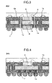
- FIG. 3 is a cross-sectional diagram of a semiconductor device in accordance with a second embodiment of the invention.
- FIG. 4 is a sectional view of semiconductor device in accordance with a third embodiment of the invention.
- FIG. 5 is a sectional view of semiconductor device in accordance with a fourth embodiment.
- FIG. 6 is an overall sectional view of an electronic control unit in accordance with a fifth embodiment.
- FIG. 7 is an enlarged partial sectional view of the apparatus shown in FIG. 6 .
- FIG. 1 a semiconductor device 100 in accordance with one preferred embodiment of the invention is depicted in cross-section. A side view of this device is shown in FIG. 2 .
- a semiconductor circuit element 6 and an electronic component 3 such as a passive element are disposed on a substrate 1 with an electronic circuit arranged thereon. These are fixed to the substrate 1 by use of a conductive adhesive agent 4 .
- the semiconductor element 6 is connected by use of bonding wires 2 to the electronic circuit on the substrate 1 . Note here that although in FIGS. 1-2 only one semiconductor element 6 is provided, two or more semiconductor elements 6 may be mounted. Additionally the substrate 1 as used herein is a printed circuit board or a flexible substrate.
- the illustrative semiconductor device 100 is resin-sealed by a thermally hardenable sealing resin material 5 , such as epoxy resin or equivalents thereof. While the semiconductor element 6 and the electronic component 3 are mounted on the side of a semiconductor element mount face 6 a , the thermal hardenable resin 5 is filled on the substrate 1 , including the semiconductor element 6 and electronic component 3 . It is desirable that the thermal hardenable resin 5 be matched in physical properties with the substrate 1 for reliability improvement purposes. To this end, the physical properties of the thermal hardenable resin 5 after hardening are preferably set so that the linear expansion coefficient falls within a range of from 7 to 25 ppm/° C. and the elasticity ranges from 7 to 30 Gpa with the glass transition temperature ranging from 70 to 200° C.
- conductive bumps 7 are provided on a principal surface of the substrate 1 on the opposite side to the semiconductor element mount face 6 a . These conductive bumps 7 are laid out to enable the semiconductor device 100 to achieve electrical connection between it and an external substrate.
- the conductive bumps 7 used here may preferably be lead-free solder bumps that are high in strength and in melting-point temperature.
- a metallic core layer 1 a is provided inside of the substrate 1 as a core material thereof.
- a counterbore 10 that is, a concave portion in the surface of substrate 1 , is provided at a portion for mounting the semiconductor element 6 , causing the semiconductor element 6 to be connected to the metallic core layer 1 a which is provided as the core material of the substrate 1 by using the conductive adhesive 4 , such as an epoxy-based adhesive agent or equivalents thereto.
- the counterbore 10 for heat radiation is disposed at a central part thereof.
- the counterbore 10 is provided with a thin metal plate 8 , which is connected via a soldering material 9 to the metallic core layer 1 a.
- parts or components corresponding to a plurality of semiconductor devices are mounted together on a single sheet, followed by dicing thereof at the last step to thereby fabricate more than two semiconductor devices 100 .
- the metallic core layer 1 a a one metal plate is disposed on the sheet; thereafter at the last step, dicing is applied thereto, resulting in fabrication of the metallic core layer 1 a . Due to this, part of the metallic core layer 1 a which was cut by dicing is exposed to an outer circumferential face if of the substrate 1 .
- the semiconductor element 6 and the electronic component 3 are connected using the conductive adhesive 4 such as silver paste or the like so that unwanted exfoliation or “peel-off” and interconnect wire disconnection no longer take place even in the case of connection using the lead-free conductive bumps 7 , which are subjected to a reflow process at high temperatures. Thus, no appreciable reliability problems occur.
- the conductive adhesive 4 such as silver paste or the like
- Ni—Au-based plating 1 e is applied to upper part of Cu-based conductors 1 d . Additionally on the metallic core layer 1 a with the semiconductor element 6 mounted thereto is applied Ni—Au plating 1 e.
- the substrate 1 be matched or “harmonized” in physical properties with the thermal hardenable resin 5 .
- the physical properties of the resin material making up the substrate 1 are preferably designed so that the linear expansion coefficient falls within a range of from 20 to 70 ppm/° C. while letting the glass transition temperature stay at 150° C. or more.
- FIG. 3 there is shown a cross-sectional view of a semiconductor device 200 in accordance with a second embodiment of the invention.
- the semiconductor device 200 is structurally different from the semiconductor device 100 of FIGS. 1-2 in that through-going holes 1 p and 1 q are provided in the substrate 1 .
- the semiconductor device 200 is principally the same in other arrangements as the semiconductor device 100 .
- the through-hole 1 q is electrically connected to the metallic core layer 1 a also. This feature is also devoted to improvements in heat releasability.
- FIG. 4 is a cross-sectional view of a semiconductor device 300 in accordance with a third embodiment of the invention.
- the semiconductor device 300 is different from the semiconductor device 100 of FIG. 1 in that some of the conductive bumps 7 are directly connected to the metallic core layer 1 a which underlies the semiconductor element 6 .
- the semiconductor device 300 is fundamentally the same in other arrangements as the semiconductor device 100 .
- the semiconductor device 300 is arranged so that the conductive bumps 7 are directly connected to the metallic core layer 1 a , it is possible to ground wires on or above the substrate 1 by the conductive bumps 7 underlying the metallic core layer 1 a .
- the metallic core layer la As the semiconductor device 300 is arranged so that the conductive bumps 7 are directly connected to the metallic core layer 1 a , it is possible to ground wires on or above the substrate 1 by the conductive bumps 7 underlying the metallic core layer 1 a .
- the metallic core layer la As the semiconductor device 300 is arranged so that the conductive bumps 7 are directly connected to the metallic core layer 1 a , it is possible to ground wires on or above the substrate 1 by the conductive bumps 7 underlying the metallic core layer 1 a .
- the conductive bumps that are provided beneath the metallic core layer 1 a function as the ground, and the metallic core layer 1 a to be connected to these conductive bumps is designed to have a specific area and thickness. This enables the semiconductor device 300 to retain
- Another advantage is that the direct connection between the metallic core layer 1 a that becomes the ground potential and the conductive bumps 7 strengthens the ground potential and thus enables mounting of large-current circuitry and power semiconductor circuit elements.
- the conductive bumps 7 as coupled to the metallic core layer 1 a are capable of offering increased reliability of more than 1,000 cycles of thermal shock tests.
- FIG. 5 is a cross-sectional view of a semiconductor device 400 in accordance with a fourth embodiment.
- the semiconductor device 400 is the one that provides a multilayered substrate structure by repeated lamination of the basic arrangement of the semiconductor device 100 shown in FIG. 1 .
- the metallic core layer 1 a is disposed on a per-substrate basis and is provided in each layer of such multilayer substrate.
- a semiconductor element 6 is electrically connected to a metallic core layer 1 a of the first layer (uppermost layer). It is connected to each metal core layer from the semiconductor element mount face 6 a through inner via holes 1 c , followed by connection to conductive bumps 7 from each metal core layer through inner via holes 1 c.
- respective ones of the metallic core layers 1 a at respective layers are adapted for use as a ground potential layer 1 k , a power supply potential layer 1 m and a power signal potential layer 1 n , thereby to constitute each metallic core layer 1 a as part of circuitry.
- a through-hole 1 b for use as a signal transmission line has a hole as defined therein to thereby ensure that it does not come into contact with the ground potential layer 1 k and/or the power supply potential layer 1 m.
- the substrate 1 has a passive circuit element 24 and an active element 25 as buried or “embedded” therein whereby it is possible to achieve miniaturization and high integration/packaging densities.
- FIGS. 6 and 7 there is shown the structure of an electronic control module 500 using a semiconductor device 18 .
- the electronic controller 500 is adaptable for use as a land vehicle engine controller, for example.
- FIG. 6 is a sectional view of an entirety of the electronic controller 500 in this embodiment, whereas FIG. 7 is an enlarged partial sectional view of main part of it.
- the electronic controller 500 has a metallic casing 11 made of aluminum or other similar suitable metals.
- the metal case 11 contains a board 19 as received therein.
- This board 19 is attached to hump-like portions or “protrusions” 11 a of the metal case 11 and fixed thereto by a silicon-based adhesive 13 .
- the board 19 is also fixed to the metal case 11 by substrate-fastening rivets 15 , thereby ensuring rigid attachment between the board 19 and the metal case 11 .
- the interior of the electronic controller 500 is air-tightly sealed by a cover 14 as attached to the metal case 11 .
- a ball grid array (BGA) 17 and semiconductor device 18 plus electronics components 33 are disposed on the board 19 .
- the electronic components 33 are mounted not only on the semiconductor device 18 -mounting principal surface side of the board 19 but also on the opposite-side principal surface thereof.
- a connector 12 is attached to the metal case 11 .
- the connector 12 has a predefined number of connection pins for electrical connection between the circuitry on the board 19 and an external device or equipment as operatively associated therewith. These pins are fixed to the board 19 .
- the connector 12 are provided at lower surface part of the metal case 11 , this is not to be construed as limiting the invention and may alternatively be arranged so that these are provided at the metal case's upper face part or its side face part.
- the semiconductor device 18 is similar in structure to the semiconductor devices as stated supra in the above-noted embodiments. More specifically, a semiconductor element 6 is mounted above a metallic core layer 1 a , and a metal plate 8 that is disposed to underlie the metallic core layer 1 a is connected to the metal core layer 1 a . Owing to this structural feature, unwanted heat as radiated from the semiconductor element 6 is efficiently released or “escaped” toward the outside from the metal core layer 1 a via the metal plate 8 .
- the BGA 17 and semiconductor device 18 have a plurality of conductive bumps 7 for the external signal input/output use. BGA 17 and semiconductor device 18 are electrically connected to the circuitry on the board 19 through these conductive bumps 7 .
- a thin metal plate 8 that is centrally disposed on the semiconductor device 18 is connected to the board 19 via a soldering material 9 .
- a large number of thermal vias 16 are disposed in the board 19 at part immediately beneath the metal plate 8 of the semiconductor device 18 .
- the thermal vias 16 are internally filled with the solder material 9 along with conductive paste. Upper part of the thermal vias 16 as filled with the solder material 9 and conductive paste is connected to the metal plate 8 of semiconductor device 18 by way of the solder material 9 .
- the protrusions 11 a of the metal case 11 are disposed on one of the both principal surfaces of the board 19 , which is on the opposite side to the principal surface to which the semiconductor device 18 is connected.
- the protrusions 11 a are coupled to the board 19 via the silicon-based adhesive 13 .
- the silicon-based adhesive 13 be designed to have its thermal conductivity of 1W/m.K or greater and a thickness of 5 mm or more.
- a heat-release grease may also be employable.
- the electronic control module of this embodiment it becomes possible to efficiently release the heat radiated from the semiconductor device 18 toward the metal case 11 through the thermal vias 16 as filled with the solder material 9 .
Abstract
Description
Claims (13)
Applications Claiming Priority (2)
| Application Number | Priority Date | Filing Date | Title |
|---|---|---|---|
| JP2005-355531 | 2005-12-09 | ||
| JP2005355531A JP2007158279A (en) | 2005-12-09 | 2005-12-09 | Semiconductor device and electronic controller using the same |
Publications (2)
| Publication Number | Publication Date |
|---|---|
| US20070145473A1 US20070145473A1 (en) | 2007-06-28 |
| US7679176B2 true US7679176B2 (en) | 2010-03-16 |
Family
ID=37772658
Family Applications (1)
| Application Number | Title | Priority Date | Filing Date |
|---|---|---|---|
| US11/635,561 Active 2027-10-23 US7679176B2 (en) | 2005-12-09 | 2006-12-08 | Semiconductor device and electronic control unit using the same |
Country Status (4)
| Country | Link |
|---|---|
| US (1) | US7679176B2 (en) |
| EP (1) | EP1796163B1 (en) |
| JP (1) | JP2007158279A (en) |
| CN (1) | CN1979836A (en) |
Cited By (6)
| Publication number | Priority date | Publication date | Assignee | Title |
|---|---|---|---|---|
| US20090014865A1 (en) * | 2007-07-10 | 2009-01-15 | Phoenix Precision Technology Corporation | Heat-conductive package structure |
| US20090189276A1 (en) * | 2008-01-30 | 2009-07-30 | Hikari Sano | Semiconductor chip and semiconductor device |
| US20100096163A1 (en) * | 2008-10-21 | 2010-04-22 | Shinko Electric Industries Co., Ltd. | Wiring board and method of manufacturing the same |
| US20110100681A1 (en) * | 2008-04-28 | 2011-05-05 | Peter Kimmich | Substrate-mounted circuit module having components in a plurality of contacting planes |
| US20140097533A1 (en) * | 2011-12-21 | 2014-04-10 | Huawei Technologies Co., Ltd. | Pop Package Structure |
| US20150351219A1 (en) * | 2011-04-15 | 2015-12-03 | Samsung Electro-Mechanics Co., Ltd. | Printed circuit board and method of manufacturing the same |
Families Citing this family (11)
| Publication number | Priority date | Publication date | Assignee | Title |
|---|---|---|---|---|
| KR20080076241A (en) * | 2007-02-15 | 2008-08-20 | 삼성전기주식회사 | Printed circuit board having electronic component and method for manufacturing thereof |
| US8410601B2 (en) | 2009-11-15 | 2013-04-02 | Microsemi Corporation | RF package |
| US8034666B2 (en) | 2009-11-15 | 2011-10-11 | Microsemi Corporation | Multi-layer thick-film RF package |
| US8772817B2 (en) | 2010-12-22 | 2014-07-08 | Cree, Inc. | Electronic device submounts including substrates with thermally conductive vias |
| CN103650134B (en) * | 2011-10-20 | 2017-08-25 | 松下电器产业株式会社 | Semiconductor device |
| CN105027278A (en) * | 2013-03-07 | 2015-11-04 | 住友电木株式会社 | Apparatus, composition for adhesive, and adhesive sheet |
| JP6587795B2 (en) * | 2014-10-02 | 2019-10-09 | 太陽誘電株式会社 | Circuit module |
| US9860987B2 (en) * | 2015-02-13 | 2018-01-02 | Deere & Company | Electronic assembly with one or more heat sinks |
| JPWO2018235484A1 (en) * | 2017-06-21 | 2020-04-23 | 住友電気工業株式会社 | Electronic circuit device |
| JP2020161508A (en) * | 2017-06-23 | 2020-10-01 | 株式会社村田製作所 | module |
| JP2020009879A (en) * | 2018-07-06 | 2020-01-16 | 太陽誘電株式会社 | Circuit board and circuit module |
Citations (19)
| Publication number | Priority date | Publication date | Assignee | Title |
|---|---|---|---|---|
| EP0981268A1 (en) | 1998-06-23 | 2000-02-23 | Nitto Denko Corporation | Circuit board with an electronic component mounted thereon and multi-layer board |
| US6097089A (en) | 1998-01-28 | 2000-08-01 | Mitsubishi Gas Chemical Company, Inc. | Semiconductor plastic package, metal plate for said package, and method of producing copper-clad board for said package |
| JP2000315747A (en) | 1999-04-28 | 2000-11-14 | Sumitomo Metal Electronics Devices Inc | Semiconductor package |
| US20010046725A1 (en) * | 1999-09-03 | 2001-11-29 | Thin Film Module, Inc. | High density cavity-up wire bond BGA |
| DE10127268A1 (en) | 2000-10-02 | 2002-04-25 | Siemens Ag | Printed circuit board as a circuit carrier with two metal outer layers and a metal intermediate layer has insulating layers between the outer and intermediate layers with a cooling component on an outer layer linked via a heat path. |
| US20020084524A1 (en) | 2001-01-04 | 2002-07-04 | Samsung Electronics Co., Ltd. | Ball grid array package comprising a heat sink |
| US20030002260A1 (en) * | 2001-05-22 | 2003-01-02 | Takehiko Hasebe | Electronic apparatus |
| JP2003046022A (en) | 2001-05-22 | 2003-02-14 | Hitachi Ltd | Electronic apparatus |
| US20030034566A1 (en) | 2000-02-14 | 2003-02-20 | Jimarez Lisa J. | Reduction of chip carrier flexing during thermal cycling |
| US6528891B2 (en) * | 1998-12-17 | 2003-03-04 | Charles Wen Chyang Lin | Bumpless flip chip assembly with solder via |
| US6528882B2 (en) * | 2000-10-04 | 2003-03-04 | Advanced Semiconductor Engineering, Inc. | Thermal enhanced ball grid array package |
| US20030184969A1 (en) * | 2002-03-28 | 2003-10-02 | Toru Itabashi | Electronic control unit |
| EP1387606A2 (en) | 2002-07-30 | 2004-02-04 | Hitachi, Ltd. | Device for controlling a vehicle |
| US20040021210A1 (en) * | 2002-07-30 | 2004-02-05 | Toshiba America Electronic Components, Inc. | Semiconductor packaging apparatus |
| US20040089943A1 (en) | 2002-11-07 | 2004-05-13 | Masato Kirigaya | Electronic control device and method for manufacturing the same |
| JP2004172425A (en) | 2002-11-21 | 2004-06-17 | Hitachi Ltd | Electronic apparatus |
| US20040125579A1 (en) * | 2002-12-27 | 2004-07-01 | Satoru Konishi | Semiconductor module |
| EP1443561A2 (en) | 2003-01-30 | 2004-08-04 | Endicott Interconnect Technologies, Inc. | Stacked chip electronic package having laminate carrier and method of making same |
| EP1571706A1 (en) | 2002-11-21 | 2005-09-07 | Hitachi, Ltd. | Electronic device |
Family Cites Families (2)
| Publication number | Priority date | Publication date | Assignee | Title |
|---|---|---|---|---|
| JP2000260900A (en) * | 1999-03-04 | 2000-09-22 | Mitsubishi Gas Chem Co Inc | Substrate for semiconductor plastic package |
| JP2005085783A (en) * | 2003-09-04 | 2005-03-31 | Mitsubishi Gas Chem Co Inc | Ball-grid-array plastic semiconductor package |
-
2005
- 2005-12-09 JP JP2005355531A patent/JP2007158279A/en active Pending
-
2006
- 2006-12-05 CN CNA200610164228XA patent/CN1979836A/en active Pending
- 2006-12-08 US US11/635,561 patent/US7679176B2/en active Active
- 2006-12-08 EP EP06025446.3A patent/EP1796163B1/en active Active
Patent Citations (19)
| Publication number | Priority date | Publication date | Assignee | Title |
|---|---|---|---|---|
| US6097089A (en) | 1998-01-28 | 2000-08-01 | Mitsubishi Gas Chemical Company, Inc. | Semiconductor plastic package, metal plate for said package, and method of producing copper-clad board for said package |
| EP0981268A1 (en) | 1998-06-23 | 2000-02-23 | Nitto Denko Corporation | Circuit board with an electronic component mounted thereon and multi-layer board |
| US6528891B2 (en) * | 1998-12-17 | 2003-03-04 | Charles Wen Chyang Lin | Bumpless flip chip assembly with solder via |
| JP2000315747A (en) | 1999-04-28 | 2000-11-14 | Sumitomo Metal Electronics Devices Inc | Semiconductor package |
| US20010046725A1 (en) * | 1999-09-03 | 2001-11-29 | Thin Film Module, Inc. | High density cavity-up wire bond BGA |
| US20030034566A1 (en) | 2000-02-14 | 2003-02-20 | Jimarez Lisa J. | Reduction of chip carrier flexing during thermal cycling |
| DE10127268A1 (en) | 2000-10-02 | 2002-04-25 | Siemens Ag | Printed circuit board as a circuit carrier with two metal outer layers and a metal intermediate layer has insulating layers between the outer and intermediate layers with a cooling component on an outer layer linked via a heat path. |
| US6528882B2 (en) * | 2000-10-04 | 2003-03-04 | Advanced Semiconductor Engineering, Inc. | Thermal enhanced ball grid array package |
| US20020084524A1 (en) | 2001-01-04 | 2002-07-04 | Samsung Electronics Co., Ltd. | Ball grid array package comprising a heat sink |
| JP2003046022A (en) | 2001-05-22 | 2003-02-14 | Hitachi Ltd | Electronic apparatus |
| US20030002260A1 (en) * | 2001-05-22 | 2003-01-02 | Takehiko Hasebe | Electronic apparatus |
| US20030184969A1 (en) * | 2002-03-28 | 2003-10-02 | Toru Itabashi | Electronic control unit |
| EP1387606A2 (en) | 2002-07-30 | 2004-02-04 | Hitachi, Ltd. | Device for controlling a vehicle |
| US20040021210A1 (en) * | 2002-07-30 | 2004-02-05 | Toshiba America Electronic Components, Inc. | Semiconductor packaging apparatus |
| US20040089943A1 (en) | 2002-11-07 | 2004-05-13 | Masato Kirigaya | Electronic control device and method for manufacturing the same |
| JP2004172425A (en) | 2002-11-21 | 2004-06-17 | Hitachi Ltd | Electronic apparatus |
| EP1571706A1 (en) | 2002-11-21 | 2005-09-07 | Hitachi, Ltd. | Electronic device |
| US20040125579A1 (en) * | 2002-12-27 | 2004-07-01 | Satoru Konishi | Semiconductor module |
| EP1443561A2 (en) | 2003-01-30 | 2004-08-04 | Endicott Interconnect Technologies, Inc. | Stacked chip electronic package having laminate carrier and method of making same |
Non-Patent Citations (1)
| Title |
|---|
| European Search Report dated Mar. 13, 2007 (Nine (9) Pages). |
Cited By (10)
| Publication number | Priority date | Publication date | Assignee | Title |
|---|---|---|---|---|
| US20090014865A1 (en) * | 2007-07-10 | 2009-01-15 | Phoenix Precision Technology Corporation | Heat-conductive package structure |
| US7786571B2 (en) * | 2007-07-10 | 2010-08-31 | Unimicron Technology Corporation | Heat-conductive package structure |
| US20090189276A1 (en) * | 2008-01-30 | 2009-07-30 | Hikari Sano | Semiconductor chip and semiconductor device |
| US8134231B2 (en) * | 2008-01-30 | 2012-03-13 | Panasonic Corporation | Semiconductor chip and semiconductor device |
| US20110100681A1 (en) * | 2008-04-28 | 2011-05-05 | Peter Kimmich | Substrate-mounted circuit module having components in a plurality of contacting planes |
| US20100096163A1 (en) * | 2008-10-21 | 2010-04-22 | Shinko Electric Industries Co., Ltd. | Wiring board and method of manufacturing the same |
| US8330050B2 (en) * | 2008-10-21 | 2012-12-11 | Shinko Electric Industries Co., Ltd. | Wiring board having heat intercepting member |
| US20150351219A1 (en) * | 2011-04-15 | 2015-12-03 | Samsung Electro-Mechanics Co., Ltd. | Printed circuit board and method of manufacturing the same |
| US20140097533A1 (en) * | 2011-12-21 | 2014-04-10 | Huawei Technologies Co., Ltd. | Pop Package Structure |
| US9318407B2 (en) * | 2011-12-21 | 2016-04-19 | Huawei Technologies Co., Ltd. | Pop package structure |
Also Published As
| Publication number | Publication date |
|---|---|
| JP2007158279A (en) | 2007-06-21 |
| EP1796163B1 (en) | 2019-07-17 |
| US20070145473A1 (en) | 2007-06-28 |
| CN1979836A (en) | 2007-06-13 |
| EP1796163A1 (en) | 2007-06-13 |
Similar Documents
| Publication | Publication Date | Title |
|---|---|---|
| US7679176B2 (en) | Semiconductor device and electronic control unit using the same | |
| JP3437369B2 (en) | Chip carrier and semiconductor device using the same | |
| US6657311B1 (en) | Heat dissipating flip-chip ball grid array | |
| KR100310398B1 (en) | Pad Array Semiconductor Device with Thermal Conductor and Manufacturing Method Thereof | |
| US5525834A (en) | Integrated circuit package | |
| US6396136B2 (en) | Ball grid package with multiple power/ground planes | |
| EP0772234A2 (en) | Integrated circuit package | |
| US7298043B2 (en) | Semiconductor device | |
| WO1997020347A1 (en) | Semiconductor device, process for producing the same, and packaged substrate | |
| WO1998040915A1 (en) | Electronic component and semiconductor device, method for manufacturing the same, circuit board have the same mounted thereon, and electronic equipment having the circuit board | |
| US20060110927A1 (en) | Package for a semiconductor device | |
| KR20070010915A (en) | Substrate having heat spreading layer and semiconductor package using the same | |
| KR100768998B1 (en) | Chip Assembly Module of Bump Connection Type Using a Multi-layer Printed Circuit Substrate | |
| KR19990023924A (en) | Electronics and Semiconductor Packages | |
| US20060197229A1 (en) | Semiconductor device | |
| EP2058860A2 (en) | Fully testable surface mount die package configured for two-sided cooling | |
| JP5358515B2 (en) | Semiconductor device and electronic control device using the same | |
| US20040262746A1 (en) | High-density chip scale package and method of manufacturing the same | |
| JP4577980B2 (en) | Mounting board | |
| JP2005039241A (en) | Intermediate substrate with semiconductor element, substrate with intermediate substrate, and structure composed of semiconductor element, intermediate substrate, and substrate | |
| JP2891426B2 (en) | Semiconductor device | |
| US20080032454A1 (en) | Thermally Enhanced BGA Package Substrate Structure and Methods | |
| JPH10256428A (en) | Semiconductor package | |
| JP5256128B2 (en) | Electronic circuit enclosure | |
| JP2004072113A (en) | Thermally strengthened integrated circuit package |
Legal Events
| Date | Code | Title | Description |
|---|---|---|---|
| AS | Assignment |
Owner name: HITACHI, LTD.,JAPAN Free format text: ASSIGNMENT OF ASSIGNORS INTEREST;ASSIGNORS:ASANO, MASAHIKO;AKUTSU, YASUO;HARADA, MASAHIDE;AND OTHERS;SIGNING DATES FROM 20061120 TO 20061122;REEL/FRAME:018985/0714 Owner name: HITACHI, LTD., JAPAN Free format text: ASSIGNMENT OF ASSIGNORS INTEREST;ASSIGNORS:ASANO, MASAHIKO;AKUTSU, YASUO;HARADA, MASAHIDE;AND OTHERS;REEL/FRAME:018985/0714;SIGNING DATES FROM 20061120 TO 20061122 |
|
| FEPP | Fee payment procedure |
Free format text: PAYOR NUMBER ASSIGNED (ORIGINAL EVENT CODE: ASPN); ENTITY STATUS OF PATENT OWNER: LARGE ENTITY |
|
| STCF | Information on status: patent grant |
Free format text: PATENTED CASE |
|
| FPAY | Fee payment |
Year of fee payment: 4 |
|
| MAFP | Maintenance fee payment |
Free format text: PAYMENT OF MAINTENANCE FEE, 8TH YEAR, LARGE ENTITY (ORIGINAL EVENT CODE: M1552) Year of fee payment: 8 |
|
| MAFP | Maintenance fee payment |
Free format text: PAYMENT OF MAINTENANCE FEE, 12TH YEAR, LARGE ENTITY (ORIGINAL EVENT CODE: M1553); ENTITY STATUS OF PATENT OWNER: LARGE ENTITY Year of fee payment: 12 |
|
| AS | Assignment |
Owner name: HITACHI AUTOMOTIVE SYSTEMS, LTD., JAPAN Free format text: DEMERGER;ASSIGNOR:HITACHI, LTD.;REEL/FRAME:058960/0001 Effective date: 20090701 |
|
| AS | Assignment |
Owner name: HITACHI ASTEMO, LTD., JAPAN Free format text: CHANGE OF NAME;ASSIGNOR:HITACHI AUTOMOTIVE SYSTEMS, LTD.;REEL/FRAME:058481/0935 Effective date: 20210101 |