US7657185B2 - Electronic interface for long reach optical transceiver - Google Patents
Electronic interface for long reach optical transceiver Download PDFInfo
- Publication number
- US7657185B2 US7657185B2 US10/764,605 US76460504A US7657185B2 US 7657185 B2 US7657185 B2 US 7657185B2 US 76460504 A US76460504 A US 76460504A US 7657185 B2 US7657185 B2 US 7657185B2
- Authority
- US
- United States
- Prior art keywords
- layer
- circuit board
- printed circuit
- receiver
- transmitter
- Prior art date
- Legal status (The legal status is an assumption and is not a legal conclusion. Google has not performed a legal analysis and makes no representation as to the accuracy of the status listed.)
- Active, expires
Links
Images


Classifications
-
- H—ELECTRICITY
- H04—ELECTRIC COMMUNICATION TECHNIQUE
- H04B—TRANSMISSION
- H04B10/00—Transmission systems employing electromagnetic waves other than radio-waves, e.g. infrared, visible or ultraviolet light, or employing corpuscular radiation, e.g. quantum communication
- H04B10/80—Optical aspects relating to the use of optical transmission for specific applications, not provided for in groups H04B10/03 - H04B10/70, e.g. optical power feeding or optical transmission through water
- H04B10/801—Optical aspects relating to the use of optical transmission for specific applications, not provided for in groups H04B10/03 - H04B10/70, e.g. optical power feeding or optical transmission through water using optical interconnects, e.g. light coupled isolators, circuit board interconnections
-
- G—PHYSICS
- G02—OPTICS
- G02B—OPTICAL ELEMENTS, SYSTEMS OR APPARATUS
- G02B6/00—Light guides; Structural details of arrangements comprising light guides and other optical elements, e.g. couplings
- G02B6/24—Coupling light guides
- G02B6/42—Coupling light guides with opto-electronic elements
- G02B6/4201—Packages, e.g. shape, construction, internal or external details
- G02B6/4246—Bidirectionally operating package structures
-
- H—ELECTRICITY
- H05—ELECTRIC TECHNIQUES NOT OTHERWISE PROVIDED FOR
- H05K—PRINTED CIRCUITS; CASINGS OR CONSTRUCTIONAL DETAILS OF ELECTRIC APPARATUS; MANUFACTURE OF ASSEMBLAGES OF ELECTRICAL COMPONENTS
- H05K1/00—Printed circuits
- H05K1/02—Details
- H05K1/0213—Electrical arrangements not otherwise provided for
- H05K1/0254—High voltage adaptations; Electrical insulation details; Overvoltage or electrostatic discharge protection ; Arrangements for regulating voltages or for using plural voltages
-
- H—ELECTRICITY
- H05—ELECTRIC TECHNIQUES NOT OTHERWISE PROVIDED FOR
- H05K—PRINTED CIRCUITS; CASINGS OR CONSTRUCTIONAL DETAILS OF ELECTRIC APPARATUS; MANUFACTURE OF ASSEMBLAGES OF ELECTRICAL COMPONENTS
- H05K1/00—Printed circuits
- H05K1/02—Details
- H05K1/0213—Electrical arrangements not otherwise provided for
- H05K1/0216—Reduction of cross-talk, noise or electromagnetic interference
- H05K1/0218—Reduction of cross-talk, noise or electromagnetic interference by printed shielding conductors, ground planes or power plane
-
- H—ELECTRICITY
- H05—ELECTRIC TECHNIQUES NOT OTHERWISE PROVIDED FOR
- H05K—PRINTED CIRCUITS; CASINGS OR CONSTRUCTIONAL DETAILS OF ELECTRIC APPARATUS; MANUFACTURE OF ASSEMBLAGES OF ELECTRICAL COMPONENTS
- H05K1/00—Printed circuits
- H05K1/02—Details
- H05K1/0296—Conductive pattern lay-out details not covered by sub groups H05K1/02 - H05K1/0295
- H05K1/0298—Multilayer circuits
-
- H—ELECTRICITY
- H05—ELECTRIC TECHNIQUES NOT OTHERWISE PROVIDED FOR
- H05K—PRINTED CIRCUITS; CASINGS OR CONSTRUCTIONAL DETAILS OF ELECTRIC APPARATUS; MANUFACTURE OF ASSEMBLAGES OF ELECTRICAL COMPONENTS
- H05K1/00—Printed circuits
- H05K1/02—Details
- H05K1/11—Printed elements for providing electric connections to or between printed circuits
- H05K1/117—Pads along the edge of rigid circuit boards, e.g. for pluggable connectors
-
- H—ELECTRICITY
- H05—ELECTRIC TECHNIQUES NOT OTHERWISE PROVIDED FOR
- H05K—PRINTED CIRCUITS; CASINGS OR CONSTRUCTIONAL DETAILS OF ELECTRIC APPARATUS; MANUFACTURE OF ASSEMBLAGES OF ELECTRICAL COMPONENTS
- H05K2201/00—Indexing scheme relating to printed circuits covered by H05K1/00
- H05K2201/07—Electric details
- H05K2201/0707—Shielding
- H05K2201/0723—Shielding provided by an inner layer of PCB
-
- H—ELECTRICITY
- H05—ELECTRIC TECHNIQUES NOT OTHERWISE PROVIDED FOR
- H05K—PRINTED CIRCUITS; CASINGS OR CONSTRUCTIONAL DETAILS OF ELECTRIC APPARATUS; MANUFACTURE OF ASSEMBLAGES OF ELECTRICAL COMPONENTS
- H05K2201/00—Indexing scheme relating to printed circuits covered by H05K1/00
- H05K2201/10—Details of components or other objects attached to or integrated in a printed circuit board
- H05K2201/10007—Types of components
- H05K2201/10121—Optical component, e.g. opto-electronic component
-
- H—ELECTRICITY
- H05—ELECTRIC TECHNIQUES NOT OTHERWISE PROVIDED FOR
- H05K—PRINTED CIRCUITS; CASINGS OR CONSTRUCTIONAL DETAILS OF ELECTRIC APPARATUS; MANUFACTURE OF ASSEMBLAGES OF ELECTRICAL COMPONENTS
- H05K2201/00—Indexing scheme relating to printed circuits covered by H05K1/00
- H05K2201/10—Details of components or other objects attached to or integrated in a printed circuit board
- H05K2201/10431—Details of mounted components
- H05K2201/10439—Position of a single component
- H05K2201/10446—Mounted on an edge
Definitions
- the present invention relates to optical communication systems and, particularly to an electronic interface for small form factor high-speed optical transceivers with high sensitivity optical receivers.
- a transceiver typically includes both a transmitter system and a receiver system.
- a fiber optical transceiver therefore, can include a receiver optical sub assembly (ROSA), a transmitter optical sub assembly (TOSA), and an electronic interface connecting the ROSA and TOSA.
- ROSA receiver optical sub assembly
- TOSA transmitter optical sub assembly
- the ROSA may include a PIN photo detector based receiver for detecting light from an optical fiber.
- a PIN photo detector based receiver for detecting light from an optical fiber.
- high sensitivity receivers are required to compensate for the optical signal loss due to long optical fibers.
- an avalanche photodiode can be utilized instead of a PIN photodiode because of its higher sensitivity and lower noise characteristics.
- the TOSA can include a laser diode and optics for coupling optical signals generated by the laser diode into a fiber.
- the electronic interface to the TOSA and ROSA includes drivers for the TOSA, receivers for the ROSA, and power supplies to power the laser diodes and the receiver chips of the ROSA and TOSA.
- the electronic circuitry of the power supplies, the transmission circuitry, and the receiver circuitry are well separated in order to minimize the amount of noise generated on the received signals and on the transmitted signals due to the electronics.
- such an arrangement can require a great deal of space for the transceiver system.
- optical transceiver systems and in particular for long reach optical transceiver systems that have a small form factor and that are arranged to minimize interference and noise on the received signals.
- a transceiver system that has a small form factor.
- a transceiver system according to the present invention includes a receiver optical sub assembly, a transmitter optical sub assembly, and an electronic interface coupled to the receiver optical sub assembly and the transmitter optical sub assembly, wherein the electronic interface utilizes a split ground arrangement in a multi-layer circuit board assembly.
- the result of the split ground, multi-layer circuit board arrangement is that a high-voltage bias supply required for high-speed transceiver functions can be shielded from the transceiver.
- internal conducting layers can operate as shields to further assist in shielding the receiver functions from the high-voltage signal generation.
- FIG. 1 shows a transceiver according to certain embodiments of the present invention.
- FIG. 2 shows a block diagram of an electronic interface according to some embodiments of the present invention.
- FIG. 3 illustrates a multi-layer board according to some embodiments of the present invention.
- FIGS. 4A-4D show a circuit diagram of an embodiment of electronic interface according to some embodiments of the present invention.
- FIGS. 5A and 5B show a first layer of a multi-layer circuit board according to the present invention.
- FIG. 6 shows a second layer of a multi-layer circuit board according to some embodiments of the present invention.
- FIG. 7 shows a third layer of a multi-layer circuit board according to some embodiments of the present invention.
- FIG. 8 shows a fourth layer of a multi-layer circuit board according to some embodiments of the present invention.
- FIG. 9 shows a fifth layer of a multi-layer circuit board according to some embodiments of the present invention.
- FIG. 10 shows a bottom layer of a multi-layer circuit board according to some embodiments of the present invention.
- FIG. 11 shows a cross section of an embodiment of multi-layer circuit board according to some embodiments of the present invention.
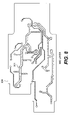
- FIG. 1 illustrates a transceiver 100 according to some embodiments of the present invention.
- transceiver 100 is housed in a metallic case (not shown).
- Transceiver 100 includes a receiver optical sub assembly (ROSA) 110 , a transceiver optical sub assembly (TOSA) 120 , and a multi-layer board 130 .
- ROSA 110 includes optics for receiving optical signals from an optical fiber and focusing the optical signals onto a detector. The detector of ROSA 110 converts the optical signals into electrical signals that are coupled to the electronic interface formed on multi-layer board 130 .
- electrical connections between ROSA 110 and the electronic interface circuit formed on multi-level board 130 include conductors for carrying a high-voltage bias voltage, a power supply voltage, a differential current signal, and a ground.
- the electrical signals and their characteristics depend on the particular optical detector and supporting circuitry housed in ROSA 110 .
- the bias voltage may be about 70 V while the power supply voltage is about 3.3 V.
- the differential voltage i.e., the voltage across the conductors carrying the differential current signal
- TOSA 120 converts electrical signals into optical signals for transmission on an optical fiber.
- TOSA 120 typically includes a laser diode and optics for coupling the light generated by the laser diode into an optical fiber and a photo diode to monitor the average optical power.
- Electrical signals into TOSA 120 can include power and ground for the laser diode as well as electrical signals to be transmitted optically over an optical fiber.
- An electronic interface circuit according to the present invention can be built on multi-level board 130 .
- Multi-level board 130 includes electrical connections to ROSA 110 and to TOSA 120 .
- multi-level board 130 includes an electrical connection 131 for making electrical connections external to transceiver 100 .
- Electrical connection 131 can be any electrical connector, for example a PCB edge finger connector.
- transceiver 100 may include covers 132 and 133 for protecting and shielding the electrical connections between ROSA 110 and the electronic interface on multi-layer board 130 and TOSA 120 and the electronic interface on multi-level board 130 .
- An embodiment of ROSA 110 that can be utilized in transceiver system 100 is disclosed in U.S. application Ser. No. 10/764,979, which is filed concurrently with the present disclosure, and is herein incorporated by reference in its entirety.
- FIG. 2 shows a simplified block diagram of an example of electronic interface 200 that can be formed on multi-layer board 130 .
- Electronic interface 200 includes electrical connection 131 where signals can be coupled to the remainder of electronic interface 200 .
- Electronic interface 200 includes a transmitter portion 240 coupled to board traces 220 .
- Transmitter portion 240 receives signals from connector 131 and provides signals to TOSA 120 through board traces 220 .
- Transmitter portion 240 can include a laser driver to control a laser diode in TOSA 120 .
- Receiver portion 230 receives signals from board traces 210 , which is coupled to ROSA 110 , and provides signals to connector 131 in response to the received signals from connector 210 .
- the signals from ROSA 110 are derived from an optical detector which, in some embodiments, can be an avalanche photodiode.
- the photodetector of ROSA 110 can require application of a large bias voltage.
- An avalanche photodiode for example, can require a bias voltage of about 70V or more. Therefore, electronic interface 200 includes a high-voltage power supply 260 that generates the bias voltage for the photodetector of ROSA 110 .
- high-voltage power supply 260 can be a DC-DC switching voltage supply.
- a low-voltage input signal e.g., a 3.3V power supply input
- a high voltage output signal e.g., about 70V
- a microcontroller system 250 can monitor and control operation of electronic interface 200 .
- Microcontroller system 250 can monitor transmitter 240 , receiver 260 , and high-voltage power supply 260 and provide status signals to connector 131 . Further, microcontroller system 250 may receive signals through connector 131 that relate to control of transmitter 240 , receiver 230 , and high-voltage power supply 260 .
- High-voltage power supply 260 can provide a large source of interference to signals in both transmitter portion 240 and receiver portion 230 . Therefore, in a transceiver system according to some embodiments of the present invention, transmitter portion 240 and receiver portion 230 are shielded from high-voltage power supply 260 .
- FIG. 3 shows an embodiment of multi-level board 130 that illustrates the configuration of electronic interface 200 .
- multi-level board 130 shown in FIG. 3 , six layers of board are formed and coupled together.
- High-voltage power supply 260 is formed on layer 301 , the top layer, of multi-level board 130 .
- Transmitter 230 and receiver 240 are formed on layer 306 , the bottom layer, which is on the opposite side of multi-layer board 130 .
- the ground of receiver 230 and on connector 210 is split from the ground of transmitter 240 in order to help shield receiver 230 from the remainder of electronic interface 200 .
- the grounds of high-voltage power supply 260 and microcomputer system 250 can be the same as the ground of transmitter 240 .
- a transceiver system includes an electronic interface arranged on a multi-level board where high-voltage power supply 260 is electrically shielded from transmitter 240 and receiver 230 .
- layer 301 will include metallic traces for the circuitry of high-voltage power supply 260 .
- Layer 301 may also include metallic traces for portions of connector 131 and connectors 220 and 210 .
- Layer 302 includes metallic vias to provide electrical connection from underlying boards to portions of connector 131 and connectors 220 and 210 (not shown).
- Layer 303 includes vias for electrical connections between boards and a copper shielding plane 307 , which may occupy some or all of layer 303 .
- Layer 304 includes metallic traces to provide interconnects between circuit elements. Electrical connections can be made through vias in other board layers.
- Layer 305 provides electrical vias between layer 304 and layer 306 .
- Layer 306 provides metallic traces for the circuitry of, for example, receiver 230 and transmitter 240 .
- Board layers 301 , 302 , 303 , 304 , 305 , and 306 are positioned in contact with one another and connections between boards can be made in well-know ways, for example by pressure, adhesives, and heating the assembly, to form multi-level board 130 .
- the components of electrical interface 260 can then be positioned on layers 301 and 306 and electrically coupled to multi-level board 130 .
- copper shielding plane 307 is a ground plane that may be floating with respect to the split-ground of electrical interface 200 .
- Copper shielding plane 307 is positioned between high-voltage power supply 260 and the circuitry of transmitter 230 and 240 in order to provide electrical shielding. Electromagnetic signals emanating from high-voltage power supply 260 , then, are blocked by shielding ground plane 307 before interfering with the signals of receiver 230 and transmitter 240 .
- Each ground, the split grounds of electronic interface 200 and copper shielding plane 307 are coupled to ground external to multi-layer board 130 .
- high-voltage power supply 260 and high-speed receiver 230 and transmitter 240 are assembled on multi-layer board 130 and the internal construction of multi-layer board 130 provides shielding to shield high-voltage power supply 260 from high-speed receiver 230 and transmitter 240 .
- Multi-layer board 130 also utilizes “blind vias” for interconnects between layers.
- FIG. 4 shows an embodiment of electrical interface 200 that can be implemented on multi-level board 130 .
- Electrical interface 200 includes a receiver portion 230 and a transmitter portion 240 .
- Receiver portion 230 includes connector 210 and amplifier 212 .
- amplifier 212 can be a MC2048C-06-T amplifier available from Mindsped, Inc.
- board trace 210 can provide connections for a bias voltage, power, ground, and a differential signal output.
- the bias voltage can be large, e.g. about 70 V.
- Power can be supplied through connector 131 and can be, for example, about 3.3 V.
- the differential signal can be filtered in an integrating filter 214 before being input to amplifier 212 .
- the output signals from amplifier 212 can be coupled to connector 131 .
- Transmitter portion 240 includes board traces 220 and laser driver 222 .
- Laser driver 222 can be, for example, a MAX3735 driver available from Maxim, Inc.
- Board traces 220 are capable of providing signal, power, and ground to TOSA 120 .
- Electronic interface 200 can be controlled by a microcontroller system 250 .
- Microcontroller system 250 can include a microcontroller 254 that can be coupled to a memory 252 where data and program instructions can be stored.
- Microcontroller 254 can be an MC3000 microcontroller available from Micrel, Inc.
- Memory 252 can, for example, be a DS18455B-50 memory chip available from Maxim, Inc.
- Microcontroller system 250 can receive signals from amplifier 212 of receiver portion 230 and from laser driver 222 of transmitter portion 240 in order to control and monitor aspects of electronic interface 200 .
- Microcontroller system 250 can also be coupled with connector 131 so that data can be communicated out of electronic interface 200 .
- Switching power supply 260 includes switch 262 , transformer 264 , and rectifier circuit 266 .
- Switching circuit 262 may, for example, be a MAX1605 switching circuit available from Maxim, Inc.
- Switching circuit 262 provides a low voltage, for example 3.3V, signal to transformer 264 .
- the low voltage signal can be a square wave signal or sine signal with frequency of about 240 kHz.
- Transformer 264 steps up the voltage to the desired high-voltage level, for example about 70V.
- Rectifier circuit 266 rectifies the signal from transformer 264 and provides a DC voltage for use, for example, in ROSA 110 as a bias voltage.
- electronic interface 200 may include further filtering and other signal shaping circuits.
- the voltage from rectifier 266 may be utilized in sampler 268 to provide a monitor signal to microprocessor 250 .
- Sampler 268 for example, can be a 1N168 chip, which can be obtained from BurrBrown, Inc.
- Switching power supply 260 in addition to providing higher DC voltages for aspects of transceiver 100 , also is a large source of noise and interference for signals received at board traces 210 and, to a lesser extent, provide noise for transmission of signals through board traces 220 . Therefore, receiver portion 230 needs to be shielded from switching power supply 260 .
- high-voltage power supply 260 can simply be separated by a large enough distance from the remainder of electronic interface 200 that the interference is minimized. This solution, however, provides for a very large form factor for transceiver system 100 .
- a split ground plane in multi-layer board 130 can be utilized to shield receiver 230 and transmitter 240 from high-voltage power supply 260 .
- the ground signals utilized in transmitter portion 240 and in high-voltage power supply 260 are split from the ground utilized in receiver portion 230 . As shown in FIG. 4 , the two grounds are indicated by the separate ground symbols ( ⁇ and ). Further, to provide further shielding, receiver portion 230 and transmitter portion 240 is primarily formed on the bottom layer of multi-layer board 130 while switching power supply 260 are primarily formed on the top layer of multi-layer board 130 .
- FIG. 5A illustrates the metal traces for layer 301 ( FIG. 3 ) of multi-layered board 130 where electronic interface 200 as illustrated in FIG. 4 is implemented. Further, the metal traces of board traces 131 , 220 and 210 are shown. Additionally, interconnections and vias are shown.
- FIG. 5B illustrates the component lay-out on layer 301 according to some embodiments of the present invention.
- transformer 264 is prominently placed on board 301 .
- switching circuit 262 is placed proximate to transformer 264 .
- Rectifier 266 which in the embodiment of electronic interface 200 shown in FIG. 4 includes diode D 1 and capacitor C 12 , is proximately arranged about transformer 264 .
- sampling circuit 268 is positioned on layer 301 . Because the signals for microcontroller 250 are of slower speed and are relatively unaffected by interference from high-voltage power supply 260 , part of microcontroller 250 can also be positioned on layer 301 . In the embodiment shown in FIG. 5B , therefore, memory 252 is positioned on layer 301 .
- FIG. 6 illustrates the arrangement of vias 600 on layer 302 of multi-layer board 130 .
- Vias 600 provide interboard interconnects in order to affect the electronic circuitry of electronic interface 200 .
- Vias 600 are “blind vias” in that, when multi-layer board 130 is assembled, electrical connections are made when the board is aligned, without specific alignment of the vias themselves.
- FIG. 7 illustrates the arrangement of vias 700 on layer 303 . Additionally, layer 303 can provide a copper plane 701 to provide electrical shielding under high-voltage power supply 260 .
- FIG. 8 illustrates electrical interconnects 801 on layer 304 .
- Interconnects 801 can provide electrical connections between vias on layer 303 and layer 305 .
- FIG. 9 illustrates vias 900 on layer 305 .
- layer 305 can also include further copper plane shielding 902 for further shielding of receiver 230 and transmitter 240 .
- FIG. 10 illustrates the arrangement of components on layer 306 .
- laser driver 222 of transmitter 240 and amplifier 212 of receiver 230 are arranged on layer 306 .
- microcontroller 250 is also mounted on layer 306 . Electrical connections between microcontroller 250 and memory 252 , which is mounted on layer 301 , are made through multi-layer board 130 .
- FIG. 11 illustrates a cross section of multi-layer board 130 .
- Layers 301 , 302 , 303 , 304 , 305 , and 306 are stacked and interconnects are made through vias 1101 in and metallic traces in multi-layer board 130 .
Abstract
Description
Claims (13)
Priority Applications (2)
| Application Number | Priority Date | Filing Date | Title |
|---|---|---|---|
| US10/764,605 US7657185B2 (en) | 2004-01-26 | 2004-01-26 | Electronic interface for long reach optical transceiver |
| PCT/US2005/002204 WO2005074172A1 (en) | 2004-01-26 | 2005-01-25 | Electronic interface for long reach optical transceiver |
Applications Claiming Priority (1)
| Application Number | Priority Date | Filing Date | Title |
|---|---|---|---|
| US10/764,605 US7657185B2 (en) | 2004-01-26 | 2004-01-26 | Electronic interface for long reach optical transceiver |
Related Child Applications (1)
| Application Number | Title | Priority Date | Filing Date |
|---|---|---|---|
| US10/617,928 Division US7074278B2 (en) | 2001-01-17 | 2003-07-10 | Removable lid and floating pivot |
Publications (2)
| Publication Number | Publication Date |
|---|---|
| US20050175350A1 US20050175350A1 (en) | 2005-08-11 |
| US7657185B2 true US7657185B2 (en) | 2010-02-02 |
Family
ID=34826488
Family Applications (1)
| Application Number | Title | Priority Date | Filing Date |
|---|---|---|---|
| US10/764,605 Active 2027-06-03 US7657185B2 (en) | 2004-01-26 | 2004-01-26 | Electronic interface for long reach optical transceiver |
Country Status (2)
| Country | Link |
|---|---|
| US (1) | US7657185B2 (en) |
| WO (1) | WO2005074172A1 (en) |
Cited By (1)
| Publication number | Priority date | Publication date | Assignee | Title |
|---|---|---|---|---|
| US20150102802A1 (en) * | 2013-10-16 | 2015-04-16 | Electronics And Telecommunications Research Institute | Optical fiber current sensor |
Families Citing this family (22)
| Publication number | Priority date | Publication date | Assignee | Title |
|---|---|---|---|---|
| US8208814B2 (en) * | 2007-04-25 | 2012-06-26 | IPhotonixs, LLC | Optical transceiver calibration system and method |
| JP2009182251A (en) * | 2008-01-31 | 2009-08-13 | Fujitsu Ltd | Optical reception sub assembly and optical reception module |
| WO2010143175A1 (en) * | 2009-06-12 | 2010-12-16 | Firecomms Limited | An optical device module and production method |
| JP2014519796A (en) | 2011-04-28 | 2014-08-14 | ゾール サーキュレイション インコーポレイテッド | Distributed distribution of battery management parameters |
| US9825475B2 (en) | 2011-04-28 | 2017-11-21 | Zoll Circulation, Inc. | System and method for automated detection of battery insert |
| EP3561995A1 (en) | 2011-04-28 | 2019-10-30 | ZOLL Circulation, Inc. | System and method for tracking and archiving battery performance data |
| US10862323B2 (en) | 2011-04-28 | 2020-12-08 | Zoll Circulation, Inc. | Battery management system for control of lithium power cells |
| CN108649655B (en) | 2011-04-28 | 2022-06-24 | 佐尔循环公司 | System for supplying power to equipment and intelligent battery pack system |
| US9437848B2 (en) | 2011-04-28 | 2016-09-06 | Zoll Circulation, Inc. | Latch mechanism for battery retention |
| US8729957B2 (en) | 2011-04-28 | 2014-05-20 | Zoll Circulation, Inc. | Battery management system with MOSFET boost system |
| US20130109331A1 (en) * | 2011-10-28 | 2013-05-02 | Broadcom Corporation | Transmit/receive switch with esd protection and methods for use therewith |
| US20130230272A1 (en) * | 2012-03-01 | 2013-09-05 | Oracle International Corporation | Chip assembly configuration with densely packed optical interconnects |
| WO2014083558A1 (en) * | 2012-11-30 | 2014-06-05 | Planxwell Ltd. | A monolithic optical receiver and a method for manufacturing same |
| US9991878B2 (en) * | 2014-08-01 | 2018-06-05 | Texas Instruments Incorporated | Cross-point shifting techniques |
| US10185103B2 (en) | 2016-03-04 | 2019-01-22 | Hisense Broadband Multimedia Technologies Co., Ltd. | Optical module |
| CN107153236B (en) * | 2016-03-04 | 2019-06-14 | 青岛海信宽带多媒体技术有限公司 | Optical module |
| US10575382B2 (en) * | 2017-04-06 | 2020-02-25 | Hisense Broadband Multimedia Technologies Co., Ltd. | Optical module |
| CN107896418B (en) * | 2017-10-10 | 2020-11-06 | 青岛海信宽带多媒体技术有限公司 | Optical module |
| TW201906312A (en) * | 2017-06-20 | 2019-02-01 | 美商蝴蝶網路公司 | Multi-stage transimpedance amplifier for ultrasonic devices |
| WO2018236779A1 (en) | 2017-06-20 | 2018-12-27 | Butterfly Network, Inc. | Amplifier with built in time gain compensation for ultrasound applications |
| US10313024B1 (en) * | 2018-04-26 | 2019-06-04 | Applied Optoelectronics, Inc. | Transmitter optical subassembly with trace routing to provide electrical isolation between power and RF traces |
| US10989870B2 (en) | 2018-08-29 | 2021-04-27 | Applied Optoelectronics, Inc. | Transmitter optical subassembly with hermetically-sealed light engine and external arrayed waveguide grating |
Citations (19)
| Publication number | Priority date | Publication date | Assignee | Title |
|---|---|---|---|---|
| US4766471A (en) | 1986-01-23 | 1988-08-23 | Energy Conversion Devices, Inc. | Thin film electro-optical devices |
| US5005939A (en) * | 1990-03-26 | 1991-04-09 | International Business Machines Corporation | Optoelectronic assembly |
| US5039194A (en) * | 1990-01-09 | 1991-08-13 | International Business Machines Corporation | Optical fiber link card |
| US5097393A (en) | 1989-05-15 | 1992-03-17 | Rogers Corporation | Multilayer interconnect device and method of manufacture thereof |
| US5202943A (en) * | 1991-10-04 | 1993-04-13 | International Business Machines Corporation | Optoelectronic assembly with alignment member |
| US5323520A (en) | 1993-04-29 | 1994-06-28 | Fujitsu Limited | Process for fabricating a substrate with thin film capacitor |
| US5479288A (en) * | 1992-05-27 | 1995-12-26 | Hitachi, Ltd. | Light transmission module |
| US5565675A (en) * | 1995-04-17 | 1996-10-15 | Hughes Electronics | Mechanically mounted optical receiver assembly |
| US5696657A (en) * | 1995-06-02 | 1997-12-09 | Hughes Electronics | Temperature compensated APD detector bias and transimpedance amplifier circuitry for laser range finders |
| US5742480A (en) * | 1994-11-02 | 1998-04-21 | Sumitomo Electric Industries, Ltd. | Optical module circuit board having flexible structure |
| US5777383A (en) * | 1996-05-09 | 1998-07-07 | Lsi Logic Corporation | Semiconductor chip package with interconnect layers and routing and testing methods |
| US6150193A (en) * | 1996-10-31 | 2000-11-21 | Amkor Technology, Inc. | RF shielded device |
| US20020140081A1 (en) * | 2000-12-07 | 2002-10-03 | Young-Huang Chou | Highly integrated multi-layer circuit module having ceramic substrates with embedded passive devices |
| US20030127704A1 (en) * | 2001-12-14 | 2003-07-10 | Kazuhiko Kobayashi | Electronic device |
| US20030142929A1 (en) | 2002-01-22 | 2003-07-31 | Meir Bartur | Flex board interface to an optical module |
| US6617518B2 (en) * | 2001-11-02 | 2003-09-09 | Jds Uniphase Corporaton | Enhanced flex cable |
| US7049676B2 (en) * | 2003-01-08 | 2006-05-23 | Oki Electric Industry Co., Ltd. | Semiconductor device having a shielding layer |
| US7136594B2 (en) * | 2001-03-06 | 2006-11-14 | Sumitomo Electric Industries, Ltd. | Optical communication device |
| US20080007930A1 (en) * | 2006-07-06 | 2008-01-10 | Fujitsu Component Limited | Photoelectric conversion module, assembling method thereof, high-speed transmission connector, and mounting system |
-
2004
- 2004-01-26 US US10/764,605 patent/US7657185B2/en active Active
-
2005
- 2005-01-25 WO PCT/US2005/002204 patent/WO2005074172A1/en active Application Filing
Patent Citations (19)
| Publication number | Priority date | Publication date | Assignee | Title |
|---|---|---|---|---|
| US4766471A (en) | 1986-01-23 | 1988-08-23 | Energy Conversion Devices, Inc. | Thin film electro-optical devices |
| US5097393A (en) | 1989-05-15 | 1992-03-17 | Rogers Corporation | Multilayer interconnect device and method of manufacture thereof |
| US5039194A (en) * | 1990-01-09 | 1991-08-13 | International Business Machines Corporation | Optical fiber link card |
| US5005939A (en) * | 1990-03-26 | 1991-04-09 | International Business Machines Corporation | Optoelectronic assembly |
| US5202943A (en) * | 1991-10-04 | 1993-04-13 | International Business Machines Corporation | Optoelectronic assembly with alignment member |
| US5479288A (en) * | 1992-05-27 | 1995-12-26 | Hitachi, Ltd. | Light transmission module |
| US5323520A (en) | 1993-04-29 | 1994-06-28 | Fujitsu Limited | Process for fabricating a substrate with thin film capacitor |
| US5742480A (en) * | 1994-11-02 | 1998-04-21 | Sumitomo Electric Industries, Ltd. | Optical module circuit board having flexible structure |
| US5565675A (en) * | 1995-04-17 | 1996-10-15 | Hughes Electronics | Mechanically mounted optical receiver assembly |
| US5696657A (en) * | 1995-06-02 | 1997-12-09 | Hughes Electronics | Temperature compensated APD detector bias and transimpedance amplifier circuitry for laser range finders |
| US5777383A (en) * | 1996-05-09 | 1998-07-07 | Lsi Logic Corporation | Semiconductor chip package with interconnect layers and routing and testing methods |
| US6150193A (en) * | 1996-10-31 | 2000-11-21 | Amkor Technology, Inc. | RF shielded device |
| US20020140081A1 (en) * | 2000-12-07 | 2002-10-03 | Young-Huang Chou | Highly integrated multi-layer circuit module having ceramic substrates with embedded passive devices |
| US7136594B2 (en) * | 2001-03-06 | 2006-11-14 | Sumitomo Electric Industries, Ltd. | Optical communication device |
| US6617518B2 (en) * | 2001-11-02 | 2003-09-09 | Jds Uniphase Corporaton | Enhanced flex cable |
| US20030127704A1 (en) * | 2001-12-14 | 2003-07-10 | Kazuhiko Kobayashi | Electronic device |
| US20030142929A1 (en) | 2002-01-22 | 2003-07-31 | Meir Bartur | Flex board interface to an optical module |
| US7049676B2 (en) * | 2003-01-08 | 2006-05-23 | Oki Electric Industry Co., Ltd. | Semiconductor device having a shielding layer |
| US20080007930A1 (en) * | 2006-07-06 | 2008-01-10 | Fujitsu Component Limited | Photoelectric conversion module, assembling method thereof, high-speed transmission connector, and mounting system |
Non-Patent Citations (1)
| Title |
|---|
| Ramaswami, R. and K.N. Sivarajan. Optical Networks: A Practical Perspective. 2nd ed. San Francisco: Morgan Kaufmann Publishers, 2002. * |
Cited By (1)
| Publication number | Priority date | Publication date | Assignee | Title |
|---|---|---|---|---|
| US20150102802A1 (en) * | 2013-10-16 | 2015-04-16 | Electronics And Telecommunications Research Institute | Optical fiber current sensor |
Also Published As
| Publication number | Publication date |
|---|---|
| US20050175350A1 (en) | 2005-08-11 |
| WO2005074172A1 (en) | 2005-08-11 |
Similar Documents
| Publication | Publication Date | Title |
|---|---|---|
| US7657185B2 (en) | Electronic interface for long reach optical transceiver | |
| US8678674B2 (en) | Optical transceiver and production method thereof | |
| US20070058980A1 (en) | Optical transceiver suppressing radiation noise form transmitter to receiver | |
| US6461058B1 (en) | Optoelectronic component | |
| US8186892B2 (en) | Optoelectronic subassembly with integral thermoelectric cooler driver | |
| US7978974B2 (en) | Insertable EMI shield clip for use in optical transceiver modules | |
| US7484967B2 (en) | Optical module with a flexible printed circuit board to be electrically connected with a host board | |
| US9348102B2 (en) | Pin cadence for high-speed connectors | |
| US9768872B2 (en) | Optical transceiver outputting wavelength multiplexed signal and receiving another wavelength multiplexed signal | |
| CN102116914B (en) | Miniaturized double-path optical module | |
| US20100098427A1 (en) | Emi shroud for a plastic receive optical subassembly | |
| US20120301154A1 (en) | Semiconductor-based optical transceiver | |
| US7338216B2 (en) | Transmitter subassembly ground return path | |
| JP2006229067A (en) | Optical transceiver module | |
| US20210103109A1 (en) | Opto-electronic assembly | |
| US9891396B2 (en) | Optical module | |
| US6407932B1 (en) | Electromagnetic interference shield and ground cage | |
| CN105122686A (en) | Receiver optical assemblies (ROAS) having photo-detector remotely located from transimpedance amplifier, and related components, and methods | |
| US20070297809A1 (en) | Optical Transmission/Reception Equipment And Optical Transmission/Reception Module | |
| JPH09171127A (en) | Optical communication module | |
| US10433447B2 (en) | Interconnect structure for coupling an electronic unit and an optical unit, and optoelectronic module | |
| US20160178862A1 (en) | Photoelectric conversion module and active fiber-optic cable | |
| CN108574018B (en) | Optical receiving module and optical module | |
| US20080170379A1 (en) | Optical Receiver Having Improved Shielding | |
| JP2007078844A (en) | Optical transmission and reception device |
Legal Events
| Date | Code | Title | Description |
|---|---|---|---|
| AS | Assignment |
Owner name: OPNEXT, INC., CALIFORNIA Free format text: ASSIGNMENT OF ASSIGNORS INTEREST;ASSIGNORS:HARTZELL, ROBERT P.;ZHANG, QINGMIN;REEL/FRAME:015591/0591 Effective date: 20040630 Owner name: OPNEXT, INC.,CALIFORNIA Free format text: ASSIGNMENT OF ASSIGNORS INTEREST;ASSIGNORS:HARTZELL, ROBERT P.;ZHANG, QINGMIN;REEL/FRAME:015591/0591 Effective date: 20040630 |
|
| STCF | Information on status: patent grant |
Free format text: PATENTED CASE |
|
| CC | Certificate of correction | ||
| FPAY | Fee payment |
Year of fee payment: 4 |
|
| FPAY | Fee payment |
Year of fee payment: 8 |
|
| AS | Assignment |
Owner name: OCLARO FIBER OPTICS, INC., CALIFORNIA Free format text: CHANGE OF NAME;ASSIGNOR:OPNEXT, INC.;REEL/FRAME:046416/0022 Effective date: 20151216 |
|
| AS | Assignment |
Owner name: DEUTSCHE BANK AG NEW YORK BRANCH, AS COLLATERAL AGENT, NEW YORK Free format text: PATENT SECURITY AGREEMENT;ASSIGNORS:LUMENTUM OPERATIONS LLC;OCLARO FIBER OPTICS, INC.;OCLARO, INC.;REEL/FRAME:047788/0511 Effective date: 20181210 Owner name: DEUTSCHE BANK AG NEW YORK BRANCH, AS COLLATERAL AG Free format text: PATENT SECURITY AGREEMENT;ASSIGNORS:LUMENTUM OPERATIONS LLC;OCLARO FIBER OPTICS, INC.;OCLARO, INC.;REEL/FRAME:047788/0511 Effective date: 20181210 |
|
| AS | Assignment |
Owner name: LUMENTUM FIBER OPTICS INC., CALIFORNIA Free format text: CHANGE OF NAME;ASSIGNOR:OCLARO FIBER OPTICS, INC.;REEL/FRAME:049843/0453 Effective date: 20190603 |
|
| AS | Assignment |
Owner name: OCLARO, INC., CALIFORNIA Free format text: RELEASE BY SECURED PARTY;ASSIGNOR:DEUTSCHE AG NEW YORK BRANCH;REEL/FRAME:051287/0556 Effective date: 20191212 Owner name: OCLARO FIBER OPTICS, INC., CALIFORNIA Free format text: RELEASE BY SECURED PARTY;ASSIGNOR:DEUTSCHE AG NEW YORK BRANCH;REEL/FRAME:051287/0556 Effective date: 20191212 Owner name: LUMENTUM OPERATIONS LLC, CALIFORNIA Free format text: RELEASE BY SECURED PARTY;ASSIGNOR:DEUTSCHE AG NEW YORK BRANCH;REEL/FRAME:051287/0556 Effective date: 20191212 |
|
| MAFP | Maintenance fee payment |
Free format text: PAYMENT OF MAINTENANCE FEE, 12TH YEAR, LARGE ENTITY (ORIGINAL EVENT CODE: M1553); ENTITY STATUS OF PATENT OWNER: LARGE ENTITY Year of fee payment: 12 |