US7655092B2 - Tandem process chamber - Google Patents
Tandem process chamber Download PDFInfo
- Publication number
- US7655092B2 US7655092B2 US10/680,656 US68065603A US7655092B2 US 7655092 B2 US7655092 B2 US 7655092B2 US 68065603 A US68065603 A US 68065603A US 7655092 B2 US7655092 B2 US 7655092B2
- Authority
- US
- United States
- Prior art keywords
- chamber
- processing
- gas
- gas distribution
- annular
- Prior art date
- Legal status (The legal status is an assumption and is not a legal conclusion. Google has not performed a legal analysis and makes no representation as to the accuracy of the status listed.)
- Expired - Fee Related, expires
Links
Images


Classifications
-
- H—ELECTRICITY
- H01—ELECTRIC ELEMENTS
- H01L—SEMICONDUCTOR DEVICES NOT COVERED BY CLASS H10
- H01L21/00—Processes or apparatus adapted for the manufacture or treatment of semiconductor or solid state devices or of parts thereof
- H01L21/67—Apparatus specially adapted for handling semiconductor or electric solid state devices during manufacture or treatment thereof; Apparatus specially adapted for handling wafers during manufacture or treatment of semiconductor or electric solid state devices or components ; Apparatus not specifically provided for elsewhere
- H01L21/67005—Apparatus not specifically provided for elsewhere
- H01L21/67011—Apparatus for manufacture or treatment
- H01L21/67155—Apparatus for manufacturing or treating in a plurality of work-stations
- H01L21/67161—Apparatus for manufacturing or treating in a plurality of work-stations characterized by the layout of the process chambers
- H01L21/67167—Apparatus for manufacturing or treating in a plurality of work-stations characterized by the layout of the process chambers surrounding a central transfer chamber
-
- H—ELECTRICITY
- H01—ELECTRIC ELEMENTS
- H01L—SEMICONDUCTOR DEVICES NOT COVERED BY CLASS H10
- H01L21/00—Processes or apparatus adapted for the manufacture or treatment of semiconductor or solid state devices or of parts thereof
- H01L21/02—Manufacture or treatment of semiconductor devices or of parts thereof
- H01L21/04—Manufacture or treatment of semiconductor devices or of parts thereof the devices having at least one potential-jump barrier or surface barrier, e.g. PN junction, depletion layer or carrier concentration layer
- H01L21/18—Manufacture or treatment of semiconductor devices or of parts thereof the devices having at least one potential-jump barrier or surface barrier, e.g. PN junction, depletion layer or carrier concentration layer the devices having semiconductor bodies comprising elements of Group IV of the Periodic System or AIIIBV compounds with or without impurities, e.g. doping materials
- H01L21/20—Deposition of semiconductor materials on a substrate, e.g. epitaxial growth solid phase epitaxy
-
- C—CHEMISTRY; METALLURGY
- C23—COATING METALLIC MATERIAL; COATING MATERIAL WITH METALLIC MATERIAL; CHEMICAL SURFACE TREATMENT; DIFFUSION TREATMENT OF METALLIC MATERIAL; COATING BY VACUUM EVAPORATION, BY SPUTTERING, BY ION IMPLANTATION OR BY CHEMICAL VAPOUR DEPOSITION, IN GENERAL; INHIBITING CORROSION OF METALLIC MATERIAL OR INCRUSTATION IN GENERAL
- C23C—COATING METALLIC MATERIAL; COATING MATERIAL WITH METALLIC MATERIAL; SURFACE TREATMENT OF METALLIC MATERIAL BY DIFFUSION INTO THE SURFACE, BY CHEMICAL CONVERSION OR SUBSTITUTION; COATING BY VACUUM EVAPORATION, BY SPUTTERING, BY ION IMPLANTATION OR BY CHEMICAL VAPOUR DEPOSITION, IN GENERAL
- C23C16/00—Chemical coating by decomposition of gaseous compounds, without leaving reaction products of surface material in the coating, i.e. chemical vapour deposition [CVD] processes
- C23C16/44—Chemical coating by decomposition of gaseous compounds, without leaving reaction products of surface material in the coating, i.e. chemical vapour deposition [CVD] processes characterised by the method of coating
- C23C16/4412—Details relating to the exhausts, e.g. pumps, filters, scrubbers, particle traps
-
- C—CHEMISTRY; METALLURGY
- C23—COATING METALLIC MATERIAL; COATING MATERIAL WITH METALLIC MATERIAL; CHEMICAL SURFACE TREATMENT; DIFFUSION TREATMENT OF METALLIC MATERIAL; COATING BY VACUUM EVAPORATION, BY SPUTTERING, BY ION IMPLANTATION OR BY CHEMICAL VAPOUR DEPOSITION, IN GENERAL; INHIBITING CORROSION OF METALLIC MATERIAL OR INCRUSTATION IN GENERAL
- C23C—COATING METALLIC MATERIAL; COATING MATERIAL WITH METALLIC MATERIAL; SURFACE TREATMENT OF METALLIC MATERIAL BY DIFFUSION INTO THE SURFACE, BY CHEMICAL CONVERSION OR SUBSTITUTION; COATING BY VACUUM EVAPORATION, BY SPUTTERING, BY ION IMPLANTATION OR BY CHEMICAL VAPOUR DEPOSITION, IN GENERAL
- C23C16/00—Chemical coating by decomposition of gaseous compounds, without leaving reaction products of surface material in the coating, i.e. chemical vapour deposition [CVD] processes
- C23C16/44—Chemical coating by decomposition of gaseous compounds, without leaving reaction products of surface material in the coating, i.e. chemical vapour deposition [CVD] processes characterised by the method of coating
- C23C16/54—Apparatus specially adapted for continuous coating
-
- H—ELECTRICITY
- H01—ELECTRIC ELEMENTS
- H01L—SEMICONDUCTOR DEVICES NOT COVERED BY CLASS H10
- H01L21/00—Processes or apparatus adapted for the manufacture or treatment of semiconductor or solid state devices or of parts thereof
- H01L21/67—Apparatus specially adapted for handling semiconductor or electric solid state devices during manufacture or treatment thereof; Apparatus specially adapted for handling wafers during manufacture or treatment of semiconductor or electric solid state devices or components ; Apparatus not specifically provided for elsewhere
- H01L21/67005—Apparatus not specifically provided for elsewhere
- H01L21/67011—Apparatus for manufacture or treatment
- H01L21/67017—Apparatus for fluid treatment
-
- H—ELECTRICITY
- H01—ELECTRIC ELEMENTS
- H01L—SEMICONDUCTOR DEVICES NOT COVERED BY CLASS H10
- H01L21/00—Processes or apparatus adapted for the manufacture or treatment of semiconductor or solid state devices or of parts thereof
- H01L21/67—Apparatus specially adapted for handling semiconductor or electric solid state devices during manufacture or treatment thereof; Apparatus specially adapted for handling wafers during manufacture or treatment of semiconductor or electric solid state devices or components ; Apparatus not specifically provided for elsewhere
- H01L21/67005—Apparatus not specifically provided for elsewhere
- H01L21/67011—Apparatus for manufacture or treatment
- H01L21/67155—Apparatus for manufacturing or treating in a plurality of work-stations
- H01L21/67161—Apparatus for manufacturing or treating in a plurality of work-stations characterized by the layout of the process chambers
- H01L21/67173—Apparatus for manufacturing or treating in a plurality of work-stations characterized by the layout of the process chambers in-line arrangement
-
- H—ELECTRICITY
- H01—ELECTRIC ELEMENTS
- H01L—SEMICONDUCTOR DEVICES NOT COVERED BY CLASS H10
- H01L21/00—Processes or apparatus adapted for the manufacture or treatment of semiconductor or solid state devices or of parts thereof
- H01L21/67—Apparatus specially adapted for handling semiconductor or electric solid state devices during manufacture or treatment thereof; Apparatus specially adapted for handling wafers during manufacture or treatment of semiconductor or electric solid state devices or components ; Apparatus not specifically provided for elsewhere
- H01L21/67005—Apparatus not specifically provided for elsewhere
- H01L21/67011—Apparatus for manufacture or treatment
- H01L21/67155—Apparatus for manufacturing or treating in a plurality of work-stations
- H01L21/6719—Apparatus for manufacturing or treating in a plurality of work-stations characterized by the construction of the processing chambers, e.g. modular processing chambers
-
- H—ELECTRICITY
- H01—ELECTRIC ELEMENTS
- H01L—SEMICONDUCTOR DEVICES NOT COVERED BY CLASS H10
- H01L21/00—Processes or apparatus adapted for the manufacture or treatment of semiconductor or solid state devices or of parts thereof
- H01L21/67—Apparatus specially adapted for handling semiconductor or electric solid state devices during manufacture or treatment thereof; Apparatus specially adapted for handling wafers during manufacture or treatment of semiconductor or electric solid state devices or components ; Apparatus not specifically provided for elsewhere
- H01L21/67005—Apparatus not specifically provided for elsewhere
- H01L21/67011—Apparatus for manufacture or treatment
- H01L21/67155—Apparatus for manufacturing or treating in a plurality of work-stations
- H01L21/67196—Apparatus for manufacturing or treating in a plurality of work-stations characterized by the construction of the transfer chamber
-
- H—ELECTRICITY
- H01—ELECTRIC ELEMENTS
- H01L—SEMICONDUCTOR DEVICES NOT COVERED BY CLASS H10
- H01L21/00—Processes or apparatus adapted for the manufacture or treatment of semiconductor or solid state devices or of parts thereof
- H01L21/67—Apparatus specially adapted for handling semiconductor or electric solid state devices during manufacture or treatment thereof; Apparatus specially adapted for handling wafers during manufacture or treatment of semiconductor or electric solid state devices or components ; Apparatus not specifically provided for elsewhere
- H01L21/67005—Apparatus not specifically provided for elsewhere
- H01L21/67011—Apparatus for manufacture or treatment
- H01L21/67155—Apparatus for manufacturing or treating in a plurality of work-stations
- H01L21/67201—Apparatus for manufacturing or treating in a plurality of work-stations characterized by the construction of the load-lock chamber
Definitions
- the present invention relates to a method and apparatus, including a system and individual system components, for concurrent processing of multiple wafers in the fabrication of integrated circuits. More particularly, the present invention provides a staged vacuum system having one or more process chambers which share one or more utilities, one or more loadlock chambers and a transfer chamber connected to both the loadlock chambers and the process chambers.
- cluster tool generally refers to a modular, multichamber, integrated processing system having a central wafer handling module and a number of peripheral process chambers.
- Cluster tools have become generally accepted as effective and efficient equipment for manufacturing advanced microelectronic devices. Wafers are introduced into a cluster tool where they undergo a series of process steps sequentially in various process chambers to form integrated circuits. The transfer of the wafers between the process chambers is typically managed by a wafer handling module located in a central transfer region.
- cluster tools are of two different types: single wafer processing or batch wafer processing.
- Single wafer processing generally refers to a chamber configuration in which a single wafer is located for processing.
- Batch wafer processing generally refers to a chamber configuration in which multiple wafers are positioned on a turntable and are processed at various positions within the chamber as the turntable rotates through 360°.
- a cluster tool configured for batch processing allows multiple wafers, typically from four (4) to seven (7) wafers, to be simultaneously processed in a single chamber.
- FIGS. 1 and 2 show examples of commercially available batch processing systems 10 .
- FIG. 1 is a top schematic view of a radial cluster tool for batch processing that is available from Novellus Corporation.
- This cluster tool includes two batch processing chambers 12 , 13 that each holds six wafers 14 for processing.
- a single wafer handling robot 16 located in a transfer chamber 18 is used to transfer wafers from a loadlock chamber 20 to a first batch processing chamber 12 one by one, where the wafers are sequentially received on a turntable 22 before receiving the same processing steps.
- the wafers may then be transferred, one by one, to a second batch processing chamber 13 , where the wafers undergo additional processing steps.
- wafers are loaded into the system one at a time and moved into a chamber where they receive partial processing at various positions as the wafers are rotated 360° on the turntable.
- FIGS. 2A and 2B are top and side schematic views of a cluster tool 10 for batch processing that is available from Mattson Technology.
- the loadlock chamber 20 and transfer chamber 18 have a common wafer elevator 19 that allow the wafers to be staged within the transfer chamber.
- a transfer robot 16 transports wafers to the processing chamber, such as a chemical vapor deposition (CVD) chamber, which holds up to four wafers. The wafers are then returned to the wafer elevator and eventually withdrawn from the tool.
- CVD chemical vapor deposition
- batch processing including the processing performed in the cluster tools described above, is that batch processing frequently provides poor deposition uniformity from the center of the wafer to the edge of the wafer. Process uniformity is important in order to obtain uniformity of deposition on the wafer.
- the poor uniformity of batch processing systems is a direct result of having multiple wafers being partially processed at multiple stations within a single chamber.
- Single wafer processing is generally considered to provide a higher degree of control over process uniformity, because a single wafer is positioned in a process chamber where it undergoes a complete process step, such as a deposition step or an etch step, without having to be moved to a different position.
- the components of a single wafer processing chamber can be positioned concentrically or otherwise relative to the single wafer.
- FIG. 3 shows a top schematic view of a cluster tool 10 having multiple single wafer processing chambers 12 mounted thereon.
- a cluster tool similar to that shown in FIG. 3 is available from Applied Materials, Inc. of Santa Clara, Calif.
- the tool includes a loadlock chamber 20 and a transfer chamber 18 having a wafer handling module 16 for moving the wafers from location to location within the system, in particular, between the multiple single wafer processing chambers 12 .
- This particular tool is shown to accommodate up to four (4) single wafer processing chambers 12 positioned radially about the transfer chamber.
- the present invention provides an apparatus for vacuum processing generally comprising an enclosure having a plurality of isolated chambers formed therein, a gas distribution assembly disposed in each processing chamber, a gas source connected to the isolated chambers, and a power supply connected to each gas distribution assembly.
- the chambers also preferably include a remote plasma system for generation of excited cleaning gases and delivery of these gases into the chamber.
- the chambers within an enclosure preferably share process gases and an exhaust system, but includes separate power sources connected to each gas distribution system.
- the chambers are configured to provide concurrent processing of multiple wafers having shared gas supplies and a shared exhaust system.
- a remote plasma system is disposed adjacent to the chambers to deliver reactive cleaning gases into the chambers.
- the chambers provide independent temperature and power control to facilitate plasma process control within each chamber.
- Each gas distribution assembly preferably includes its own power supply and related power control.
- Each pedestal also preferably including a temperature controlled member and a temperature control.
- FIG. 1 is a top schematic view of a radial cluster tool for batch processing that is available from Novellus Corporation;
- FIGS. 2A and 2B are top and side schematic views of a linear cluster tool for batch processing that is available from Mattson Technology;
- FIG. 3 is a top schematic view of a cluster tool having a plurality of single wafer processing chambers
- FIG. 4 is a perspective view of one embodiment of the vacuum processing system of the present invention.
- FIG. 5 is a top schematic view of one embodiment of the vacuum processing system of the present invention.
- FIG. 6 is a front end view of one embodiment of the vacuum processing system of the present invention.
- FIG. 7 is a back end view of one embodiment of the vacuum processing system of the present invention.
- FIG. 8 is a perspective view of the front end loading system of the present invention.
- FIG. 9 is a substantially front perspective view of the inside of a loadlock chamber of the present invention.
- FIG. 10 is a cross sectional view of a loadlock chamber of the present invention.
- FIG. 11 is a perspective view of a loadlock chamber showing a gate valve and actuating assembly mounted on the front of the loadlock chamber;
- FIG. 12 is a perspective view of another embodiment of a loadlock chamber of the present invention.
- FIG. 13 is a top view of the present invention showing a transfer chamber having a transfer wafer handling member located therein and a front end platform having two wafer cassettes and a front end wafer handling member mounted thereon for wafer mapping and centering;
- FIG. 14 is a cross sectional side view of a transfer chamber of the present invention.
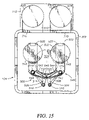
- FIG. 15 is a top view of a transfer chamber and a processing chamber showing a wafer handling member of the present invention mounted in the transfer chamber and in a retracted position ready for rotation within the transfer chamber or extension into another chamber;
- FIG. 16 is a top view of a transfer chamber and a processing chamber showing a wafer handling member of the present invention mounted in the transfer chamber and in an extended position wherein the blades are positioned in the processing chamber;
- FIG. 17 is a cross sectional view of a magnetically coupled actuating assembly of a wafer handling system of the present invention.
- FIG. 18 is a perspective view of one embodiment of a processing chamber of the present invention.
- FIG. 19 is a cross sectional view of one embodiment of a processing chamber of the present invention.
- FIG. 20 is an exploded-view of the gas distribution assembly
- FIG. 21 is a top view of a processing chamber of the present invention with the lid removed;
- FIG. 22 a is a schematic diagram of a vacuum system of the present invention.
- FIG. 22 b is a schematic diagram of another vacuum system of the present invention.
- FIG. 23 is a perspective view of a remote plasma chamber mounted on a processing chamber
- FIG. 24 is a cross sectional view of a remote plasma chamber mounted on a processing chamber.
- FIG. 25 is an illustrative block diagram of the hierarchical control structure of a computer program for process control
- FIG. 26 is a top view of a transfer chamber showing a time optimal path for a robot of the present invention.
- FIG. 27 is a graph showing the optimal velocity profile for the path shown in FIG. 26 ;
- FIG. 28 is a top view of a transfer chamber showing a time optimal path for a robot of the present invention.
- FIG. 29 is a graph showing the optimal velocity profile for the path shown in FIG. 28 .
- the present invention generally provides a cassette-to-cassette vacuum processing system which concurrently processes multiple wafers and combines the advantages of single wafer process chambers and multiple wafer handling for high quality wafer processing, high wafer throughput and reduced system footprint.
- the system is preferably a staged vacuum system which generally includes a loadlock chamber for introducing wafers into the system and which also provides wafer cooling following processing, a transfer chamber for housing a wafer handler, and one or more processing chambers each having two or more processing regions which are isolatable from each other and preferably share a common gas supply and a common exhaust pump.
- Isolatable means that the processing regions have a confined plasma zone separate from the adjacent region which is selectively communicable with the adjacent region via an exhaust system.
- the processing regions within each chamber also preferably include separate gas distribution assemblies and RF power sources to provide a uniform plasma density over a wafer surface in each processing region.
- the processing chambers are configured to allow multiple, isolated processes to be performed concurrently in at least two regions so that at least two wafers can be processed simultaneously in separate processing regions with a high degree of process control provided by shared gas sources, shared exhaust systems, separate gas distribution assemblies, separate RF power sources, and separate temperature control systems.
- the terms processing regions a chamber may be used to designate the zone in which plasma processing is carried out.
- FIGS. 4-7 illustrate the processing system 100 of the present invention schematically.
- the system 100 is a self-contained system having the necessary processing utilities supported on a main frame structure 101 which can be easily installed and which provides a quick start up for operation.
- the system 100 generally includes four different regions, namely, a front end staging area 102 where wafer cassettes 109 (shown in FIG. 8 ) are supported and wafers are loaded into and unloaded from a loadlock chamber 112 , a transfer chamber 104 housing a wafer handler, a series of tandem process chambers 106 mounted on the transfer chamber 104 and a back end 108 which houses the support utilities needed for operation of the system 100 , such as a gas panel 103 , power distribution panel 105 and power generators 107 .
- the system can be adapted to accommodate various processes and supporting chamber hardware such as CVD, PVD and etch.
- the embodiment described below will be directed to a system employing a DCVD process, such as a silane process, to deposit silicon oxide.
- a DCVD process such as a silane process
- FIG. 8 shows the front end staging area 102 of the system 100 which includes a staging platform 110 having one or more wafer cassette turntables 111 rotationally mounted through the platform 110 to support one, or more wafer cassettes 109 for processing. Wafers housed in the wafer cassettes 109 are loaded into the system 100 through one or more doors 137 disposed through a front cover 139 (both shown in FIG. 6 ).
- a front end wafer handler 113 such as a robot, is mounted on the staging platform 110 adjacent to the wafer cassette turntables 111 and the loadlock chamber door 209 (shown in FIG. 11 ).
- the front end wafer handler 113 includes a wafer mapping system to index the wafers in each wafer cassette 109 in preparation for loading the wafers into a loadlock cassette disposed in the loadlock chamber 112 .
- a wafer mapping system to index the wafers in each wafer cassette 109 in preparation for loading the wafers into a loadlock cassette disposed in the loadlock chamber 112 .
- One wafer handler used to advantage in the present system which includes a wafer mapping system is available from Equippe Technologies, Sunnyvale, Calif., as model nos. ATM 107 or 105 .
- the wafer mapping sensor verifies the number of wafers and orientation of the wafers in the cassette 109 before positioning the wafers in the loadlock chamber 112 for processing.
- An exhaust system such as ULPA filter, available from Enviroco Corporation located in Alburquerque, N.
- Mex.; Flanders located in San Rafael, Calif., or Filtra located in Santa Ana, Calif. is mounted to the, bottom of a, support shelf 115 above the platform 110 to provide particle control on the front end of the system.
- a computer monitor 117 is supported on a monitor shelf 119 above the support shelf 115 to provide touch control to an operator.
- FIG. 9 shows a substantially side perspective view of one embodiment of a loadlock chamber 112 of the present invention.
- the loadlock chamber 112 includes a sidewall 202 , a bottom 204 and a lid 206 .
- the sidewall 202 defines a loadlock loading port 208 for loading wafers into and unloading wafers out of the vacuum system 100 .
- Passages 210 and 212 are disposed in the sidewall 202 opposite the loading port 208 to allow wafers to be moved from the loadlock chamber 112 into the transfer chamber 104 (not shown).
- Slit valves and slit valve actuators are used to seal the passages 210 and 212 when isolation or staged vacuum is desired.
- a service port 214 and service door or window 216 are disposed on one end of the loadlock chamber 112 to provide service and visual access to the loadlock chamber 112 .
- a loadlock cassette 218 is disposed within the loadlock chamber 112 to support the wafers in a spaced relationship in the loadlock chamber 112 so that a wafer handler can pass between the wafers to place and remove wafers from the loadlock cassette 218 .
- the loadlock cassette 218 preferably supports two or more wafers in a side-by-side arrangement on wafer seats 220 .
- the wafer seats 220 are formed on cassette plates 222 which are supported in spaced relation on a movable shaft 224 .
- the plates 222 are made of anodized aluminum and can handle up to about 14 wafers spaced vertically apart by about 0.6 inch. In the embodiment shown in FIG. 9 , six rows of wafer seats 220 are provided to support a total of twelve (12) wafers.
- Each wafer seat 220 defines at least two grooves 226 in which a support rail 228 is disposed to support a wafer above the wafer seat 220 to provide a cooling gas passage below the wafer.
- a support rail 228 is disposed to support a wafer above the wafer seat 220 to provide a cooling gas passage below the wafer.
- at least two rails 228 made of a ceramic are provided to support the wafer, but more rails may be used. Wafers are supported about 1 to about 15 mils above the wafer seats 220 on the ceramic rails 228 to provide uniform cooling of the wafers.
- the shaft 224 is disposed through the bottom 204 of the loadlock chamber 112 and supports the cassette plates 222 within the loadlock chamber 112 .
- a motor such as a stepper motor or other elevator system, is disposed below the bottom 204 of the loadlock chamber 112 and moves the shaft 224 upwardly and downwardly within the loadlock chamber 112 to locate a pair of wafers in alignment with a wafer handler for loading or unloading wafers from the loadlock chamber 112 .
- FIG. 10 shows a side view of the loadlock chamber 112 with the front removed.
- the cassette plates 222 include a central portion 230 through which the shaft 224 extends to support the plates 222 .
- the outer edges of the cassette plates 222 are supported in a spaced relationship by spacers 232 which are secured thereto with pins 234 .
- Each plate 222 defines a central channel 236 formed into each plate to form a slot for the robot blade to pass under the wafer when, the wafer is supported on the seat 220 .
- FIG. 11 shows a front perspective view of the loadlock chamber 112 .
- Loading door 209 and door actuator 238 are shown in a closed and sealed position.
- the loading door 209 is connected to the actuator 238 on movable shafts 240 .
- the actuator 238 tilts away from the side wall 202 to unseal the door 209 and then the shafts 240 are lowered to provide clearance of the door 209 and access to the port 208 (shown in FIG. 9 ).
- One door actuator used to advantage with the present invention is available from VAT, located in Switzerland.
- An on-board vacuum pump 121 is mounted on the frame 101 adjacent the loadlock chamber 112 and the transfer chamber 104 to pump down the loadlock chamber and the transfer chamber.
- An exhaust port 280 is disposed through the bottom of the loadlock chamber 112 and is connected to the pump 121 via exhaust line 704 .
- the pump is preferably a high vacuum turbo pump capable of providing milliTorr pressures with very low vibration.
- One vacuum used to advantage is available from Edward High Vacuum.
- the transfer chamber 104 is preferably pumped down through the loadlock chamber 112 by opening a pair of slit valves sealing passages 210 , 212 and pumping gases out through the exhaust port 280 located in the loadlock chamber 112 . Gas-bound particles are kept from being swept into the transfer chamber 104 by continually exhausting gases out of the system through the loadlock chamber 112 .
- a gas diffuser 231 is disposed in the loadlock chamber to facilitate venting up to atmosphere.
- the gas diffuser 231 is a preferably a conduit disposed in the loadlock chamber and connected to a gas purge line such as an N 2 purge gas line.
- the gas diffuser 231 distributes the purge gas along a larger surface area through a plurality of ports 233 disposed along the length of the diffuser, thereby decreasing the time needed to vent the chamber up to atmosphere.
- the vacuum system of the present invention will be described in more detail below.
- FIG. 12 shows a cut-away perspective view of another embodiment of a loadlock chamber 112 of the present invention.
- the loadlock chamber 112 includes chamber walls 202 , a bottom 204 , and a lid 206 .
- the chamber 112 includes two separate environments or compartments 242 , 244 and a transfer region 246 .
- Compartments 242 , 244 include a wafer cassette in each compartment 242 , 244 to support the wafers therein.
- Each compartment 242 , 244 includes a support platform 248 and a top platform 250 to define the bottom and top of the compartments 242 , 244 .
- a support wall 252 may be disposed vertically within the compartments 242 , 244 to support platforms 248 , 250 in a spaced relationship.
- Transfer region 246 includes one or more passages 192 for providing access from the loadlock chamber 112 into the transfer chamber 104 (not shown). Passages 192 are preferably opened and closed using slit valves and slit valve
- Compartments 242 , 244 are each connected to an elevator shaft 224 , each of which is connected to a motor, such as a stepper motor or the like, to move the compartments upwardly or downwardly within the loadlock chamber 112 .
- a sealing flange 256 is disposed peripherally within the loadlock chamber 112 to provide a sealing surface for support platform 248 of compartment 242 .
- Sealing flange 258 is similarly disposed to provide a sealing surface for support platform 250 of compartment 244 .
- the compartments 242 , 244 are isolated from one another by sealing flanges 256 , 258 to provide independent staged vacuum of the compartments 242 , 244 within the loadlock chamber 112 .
- a back side pressure is maintained in spaces 260 , 262 through a vacuum port disposed therein.
- a vacuum pump is connected to the spaces 260 , 262 via exhaust lines 264 so that a high vacuum can be provided in the spaces 260 , 262 to assist in sealing the platforms 248 , 250 against the sealing flanges 256 , 258 .
- compartments 242 , 244 can be loaded or unloaded in the position shown in FIG. 12 .
- Loading doors 209 and actuators 238 are provided through the front wall (not shown) at the upper and lower limits of the loadlock chamber 112 corresponding with compartments 242 , 244 .
- the pressure in a selected compartment is pumped down after wafers have been, loaded into the compartment via exhaust lines 287 , 289 and the selected compartment is moved into the transfer region 246 .
- Compartments 242 , 244 move independently into the transfer region 246 by the stepper motor.
- the advantage of having upper and lower compartments 242 , 244 is that processing of one set of wafers can occur while a second set of wafers is loaded into the other compartment and that compartment is pumped down to the appropriate pressure so that the compartment can be moved into the transfer region 246 and in communication with the transfer chamber 104 .
- FIG. 8 shows the wafer handling robot 113 on the front end 102 of the system 100 which includes a wafer transfer blade for transferring wafers from the wafer cassettes 109 into and out of the loadlock chamber 112 .
- the wafers do not always lie in precisely the same position within each wafer cassette 109 and, therefore, are not positioned identically on the blade when they are transferred into the loadlock cassette 218 .
- the precise location of the wafer on the robot blade must be determined and provided to a controlling computer.
- Knowing the exact center of the wafers allows the computer to adjust for the variable position of each wafer on the blade and deposit the wafer precisely in the desired position in a loadlock cassette 218 so that, ultimately, the wafer handler in the transfer chamber can precisely position the wafers in the process chambers 106 .
- An optical sensing system 170 which provides wafer position data (preferably the center coordinate of the wafer) to enable the robot to precisely position the wafers in, the loadlock cassette 218 is provided adjacent to each cassette turntable 111 on the front end 102 .
- Each system comprises three optical sensors 172 mounted on the lower support 173 of a C clamp 174 adjacent the cassette turntable 111 along a line perpendicular to the path of the robot blade and three optical emitters 176 positioned on the upper support 177 of the C clamp 174 aligned with the associated sensors so that the sensors intercept the light beams from the associated emitters.
- each pair comprises a conventional infrared emitter and sensor.
- the output of the sensors is converted by associated analog to, digital converters into digital signals which are applied as input to the system computer for use in computing the center coordinate of the wafers as they enter the loadlock chamber 112 , and controlling the operation of the robot drive motors as required to enable precise positioning of each wafer in the loadlock cassette 218 by the robot 113 .
- the sensing and motor control circuitry are described in more detail in U.S. Pat. No. 4,819,167, by Cheng et al., which is incorporated herein by reference.
- FIG. 13 shows a top view of the processing system 100 of the present invention.
- the transfer chamber body includes sidewalls 302 and bottom 304 and is preferably machined or otherwise fabricated from one piece of material, such as aluminum.
- a lid (not shown) is supported on the sidewalls 302 during operation to form a vacuum enclosure.
- the sidewall 302 of transfer chamber 104 supports processing chambers 106 and loadlock chamber 112 .
- the sidewall 302 defines at least two passages 310 on each side through which access to the other chambers on the system is provided.
- Each of the processing chambers 106 and loadlock chamber 112 include one or more slit valve openings and slit valves which enable communication between the processing chambers, the loadlock chamber and the transfer chamber while also providing vacuum isolation of the environments within each of these chambers to enable a staged vacuum within the system.
- the bottom 304 of the transfer chamber 104 defines, a central passage 306 in which a wafer handler 500 , such as a robot assembly, extends and is mounted to the bottom of the transfer chamber.
- the bottom 304 defines a plurality of passages 308 through which one or more slit valve actuators extend and are sealably mounted.
- a gas purge port 309 is disposed through the bottom 304 of the transfer chamber 104 to provide a purge gas during pump down.
- FIG. 14 shows the transfer chamber 104 in partial cross-section.
- the passages 310 disposed through the sidewalls 302 can be opened and closed using two individual slit valves or a tandem slit valve assembly.
- the passages 310 mate with the wafer passages 610 in process regions 618 , 620 (shown in FIG. 15 ) to allow entry of wafers 502 into the processing regions 618 , 620 in chambers 106 for positioning on the wafer heater pedestal 628 .
- FIG. 15 shows a top schematic view of a magnetically coupled robot 500 of the present invention in a retracted position for rotating freely within the transfer chamber 104 .
- a robot having dual wafer handling blades 520 , 522 is located within the transfer chamber 104 to transfer the wafers 502 from one chamber to another.
- a “very high productivity” (VHP) type robot which can be modified and used to advantage in the present invention is the subject of U.S. Pat. No. 5,469,035 issued on Nov. 21, 1995, entitled “Two-axis Magnetically Coupled Robot”, and is incorporated herein by reference.
- the magnetically coupled robot 500 comprises a frog-leg type assembly connected between two vacuum side hubs (also referred to as magnetic clamps) and dual wafer blades 520 , 522 to provide both radial and rotational movement of the robot blades within a fixed plane. Radial and rotational movements can be coordinated or combined in order to pickup, transfer and deliver two wafers from one location within the system 100 to another, such as from one processing chamber 106 to another chamber.
- the robot includes a first strut 504 rigidly attached to a first magnet clamp 524 at point 525 and a second strut 506 rigidly attached to a second magnet clamp 526 (disposed concentrically below the first magnet clamp 524 ) at point 527 (See also FIG. 17 ).
- a third strut 508 is attached by a pivot 510 to strut 504 and by a pivot 512 to the wafer blade assembly 540 .
- a fourth strut 514 is attached by a pivot 516 to strut 506 and by a pivot 518 to the wafer blade assembly 540 .
- struts 504 , 508 , 506 , 514 and pivots 510 , 512 , 516 , 518 form a “frog leg” type connection between the wafer blade assembly 540 and the magnet clamps 524 , 526 .
- robot 500 When magnet clamps 524 , 526 rotate in the same direction with the same angular velocity, then robot 500 also rotates about axis A in this same direction with the same velocity. When magnet clamps 524 , 526 rotate in opposite directions with the same absolute angular velocity, then there is no rotation of assembly 500 , but instead, there is linear radial movement of wafer blade assembly 540 to a position illustrated in FIG. 16 .
- Two wafers 502 are shown loaded on the wafer blade assembly 540 to illustrate that the individual wafer blades 520 , 522 can be extended through individual wafer passages 310 in sidewall 302 of the transfer chamber 104 to transfer the wafers 502 into or out of the processing regions 618 , 620 of the chambers 106 .
- the magnetically coupled robot 500 is controlled by the relative rotational motion of the magnet clamps 524 , 526 corresponding to the relative speed of two motors.
- a first operational mode is provided in which both motors cause the magnet clamps 524 , 526 to rotate in the same direction at the same speed.
- the robot will merely rotate about a central axis A, typically from a position suitable for wafer exchange with one pair of processing regions 618 , 620 to a position suitable for wafer exchange with another pair of processing regions. Furthermore, as the fully retracted robot is rotated about the central axis A, the outermost radial points 548 along the edge of the wafer define a minimum circular region 550 required to rotate the robot.
- the magnetically coupled robot also provides a second mode in which both motors cause the magnet clamps 524 , 526 to rotate in opposite directions at the same speed.
- This second mode is used to extend the wafer blades 520 , 522 of the wafer blade assembly 640 through the passages 310 and into the processing regions 618 , 620 or, conversely, to withdraw the blades therefrom.
- Other combinations of motor rotation can be used to provide simultaneous extension or retraction of the wafer blade assembly 540 as the robot 500 is being rotated about axis A.
- an interlocking mechanism is used between the pivots or cams 512 , 518 to assure an equal and opposite angular, rotation of each pivot.
- the interlocking mechanism may take on many designs, including intermeshed gears or straps pulled around the pivots in a figure-8 pattern or the equivalent.
- One preferred interlocking mechanism is a pair of metal straps 542 , and 544 that are coupled to and extend between the pivots. 512 , 518 of the wafer blade assembly 540 .
- the straps 542 , 544 cooperate to form a figure-8 around the pivots 512 , 518 .
- the straps 542 , 544 be individually adjustable and positioned one above the other.
- a first end of the first strap 542 may pass around the back side of pivot 512 and be fixedly coupled thereto, while a second end passes around the front side of pivot 518 and is adjustably coupled, thereto.
- a first end of the second strap 544 may pass around the back side of pivot 518 and be fixedly coupled thereto, while a second end passes around the front side of pivot 512 and is adjustably coupled thereto.
- the adjustable couplings between the straps and the front sides of the pivots 512 , 518 are preferably provided with a spring that pulls a precise tension on the strap. Once the tension is established, the end of the strap is firmly held in position with a screw or other fastener.
- the straps are also shown passing around a rod 546 at the base of the U-shaped dual blade.
- FIG. 16 shows the robot arms and blade assembly of FIG. 15 in an extended position. This extension is accomplished by the simultaneous and equal rotation of magnet clamp 526 in a clock-wise direction and magnet clamp 524 in a counter-clockwise rotation.
- the individual blades 520 , 522 of the wafer blade assembly 540 are sufficiently long to extend through the passages 310 and center the wafers 502 over the pedestals 628 (See FIG. 19 ). Once the wafers 502 have been lifted from the blades by a pair of lift pin assemblies, then the blades are retracted and the passages 310 are closed by a slit valve and actuator as described above.
- FIG. 17 shows a cross sectional view of a robot drive system mounted to the central opening 306 in the bottom 304 of the transfer chamber 104 .
- the magnetic coupling assembly is configured to rotate magnetic retaining rings 524 , 526 about the central axis A, thereby providing a drive mechanism to actuate the wafer blade assembly 540 within the system, both rotationally and linearly. Additionally, the magnetic coupling assembly provides rotational movement of the magnetic retaining rings 524 , 526 with minimal contacting moving parts within the transfer chamber 104 to minimize particle generation.
- the robot features are provided by fixing first and second stepper or servo motors in a housing located above or below the transfer chamber 104 , preferably below, and coupling the output of the motors to magnetic ring assemblies located inwardly of and adjacent to a thin wall 560 .
- the thin wall 560 is connected to the upper or lower wall 304 of the transfer chamber 104 at a sealed connection to seal the interior of the transfer chamber from the environment outside of the chamber.
- Magnetic retaining rings 524 , 526 are located on the vacuum side of transfer chamber 104 , adjacent to and surrounding the thin wall 560 .
- a first motor output 562 drives a first shaft 572 and intermeshed gears 580 to provide rotation to the first magnetic ring assembly 582 that is magnetically coupled to the first magnetic retaining ring 524 .
- a second motor output 564 drives a second shaft 586 and intermeshed gears 590 to provides rotation to the second magnetic ring assembly 592 . (a concentric cylindrical member disposed about assembly 582 ) that is magnetically coupled to a second magnetic retaining ring 526 .
- Rotation of each motor provides rotational outputs 562 , 564 that rotate the magnet ring assemblies 582 , 592 which magnetically couple the rotary output through the thin wall 560 to magnetic retaining rings 524 , 526 , thereby rotating the struts 504 , 506 , respectively, and imparting rotational and translational motion to the wafer blade assembly 540 .
- each magnet ring assembly 582 , 592 and magnetic retaining ring 524 , 526 preferably include an equal plurality of magnets paired with one another through wall 560 .
- the magnets may be positioned with their poles aligned vertically, with pole pieces extending therefrom and toward the adjacent magnet to which it is coupled. The magnets which are coupled are flipped, magnetically, so that north pole to south pole coupling occurs at each pair of pole pieces located on either side of the thin walled section. While magnetic coupling is preferred, direct coupling of the motors to the retaining rings may also be employed.
- the movement of the robot 500 while transferring wafers is primarily constrained by reliance on friction between the wafer and the dual wafer blades 520 , 522 for gripping the wafers. Both linear and rotational movement of each wafer blade 520 , 522 must be controlled to avoid misalignment of the wafers. Movement of the robot is preferably optimized to provide a minimum wafer transfer time to improve productivity while avoiding wafer misalignment.
- a mathematical solution to optimization of robot movement typically involves the solution of multiple algebraic equations and non-linear differential equations or non-linear matrix differential equations, and is preferably assisted by a computer.
- persons skilled in the optimization methods can often identify the more optimum path without resolving the matrices or the equations.
- FIGS. 26-29 show the optimal paths 1500 , 1502 , 1504 for moving wafers between chambers positioned 180° apart on the processing platform and
- FIG. 27 shows the optimal velocity profile for a path 1500 halfway between paths 1502 , 1504 taken by wafers on the dual wafer blades 520 , 522 .
- FIG. 28 shows the optimal paths 1510 , 1512 , 1514 for moving wafers between chambers positioned 90° apart on the processing platform and
- FIG. 29 shows the optimal velocity profile for a path 1510 halfway between paths 1512 , 1514 taken by wafers on the dual wafer blades 520 , 522 .
- FIGS. 27 and 29 also show the maximum velocities which can be attained by the robot 500 along the paths 1500 , 1510 when wafers are not positioned on the dual wafer blades 520 , 522 .
- the robot 500 is preferably controlled so that the dual wafer blades 520 , 522 follow the optimal paths using the optimal velocity profiles shown in FIGS. 26-29 when moving wafers through the transfer chamber 104 .
- FIG. 18 shows a perspective view of one embodiment of a tandem processing chamber 106 of the present invention.
- Chamber body 602 is mounted or otherwise connected to the transfer chamber 104 and includes two processing regions in which individual wafers are concurrently processed.
- the chamber body 602 supports a lid 604 which is hindgedly attached to the chamber body 602 and includes one or more gas distribution systems 608 disposed therethrough for delivering reactant and cleaning gases into multiple processing regions.
- FIG. 19 shows a schematic cross-sectional view of the chamber 106 defining two processing regions 618 , 620 .
- Chamber body 602 includes sidewall 612 , interior wall 614 and bottom wall 616 which define the two processing regions 618 , 620 .
- the bottom wall 616 in each processing region 618 , 620 defines at least two passages 622 , 624 through which a stem 626 of a pedestal heater 628 and a rod 630 of a wafer lift pin assembly are disposed, respectively.
- a pedestal lift assembly and the wafer lift will be described in detail below.
- the sidewall 612 and the interior wall 614 define two cylindrical annular processing regions 618 , 620 .
- a circumferential pumping channel 625 is formed in the chamber walls defining the cylindrical processing regions. 618 , 620 for exhausting gases from the processing regions 618 , 620 and controlling the pressure within each region 618 , 620 .
- a chamber liner or insert 627 preferably made of ceramic or the like, is disposed in each processing region 618 , 620 to define the lateral boundary of each processing region and to protect the chamber walls 612 , 614 from the corrosive processing environment and to maintain an electrically isolated plasma environment between the electrodes.
- the liner 627 is supported in the chamber on a ledge 629 formed in the walls 612 , 614 of each processing region 618 , 620 .
- the liner includes a plurality of exhaust ports 631 , or circumferential slots, disposed therethrough and in communication with the pumping channel 625 formed in the chamber walls.
- the height of the ports relative to the face plate of the gas distribution system is controlled to provide an optimal gas flow pattern over the wafer during processing.
- FIG. 21 shows a cross sectional view of the chamber illustrating the exhaust system of the present invention.
- the pumping channels 625 of each processing region 618 , 620 are preferably connected to a common exhaust pump via a common exhaust channel 619 .
- the exhaust channel 619 is connected to the pumping channel 625 of each region 618 , 620 by exhaust conduits 621 .
- the exhaust channel 619 is connected to an exhaust pump via an exhaust line (not shown).
- Each region is preferably pumped down to a selected pressure by the pump and the connected exhaust system allows equalization of the pressure within each region.
- each of the processing regions 618 , 620 also preferably include a gas distribution assembly 608 disposed through the chamber lid 604 to deliver gases into the processing regions 618 , 620 , preferably from the same gas source.
- the gas distribution system 608 of each, processing region includes a gas inlet passage 640 which delivers gas into a shower head assembly 642 .
- the shower head assembly 642 is comprised of an annular base plate 648 having a blocker plate 644 disposed intermediate a face plate 646 .
- An RF feedthrough provides a bias potential to the showerhead assembly to facilitate generation of a plasma between the face plate 646 of the showerhead assembly and the heater pedestal 628 .
- a cooling channel 652 is formed in a base plate 648 of each gas distribution system.
- An inlet 655 delivers a coolant fluid, such as water or the like, into the channels 652 which are connected to each other by coolant line 657 .
- the cooling fluid exits the channel through a coolant outlet 659 .
- the cooling fluid is circulated through the manifold.
- the chamber body 602 defines a plurality of vertical gas passages for each reactant gas and cleaning gas suitable for the selected process to be delivered in the chamber through the gas distribution system.
- Gas inlet connections 641 are disposed at the bottom of the chamber 106 to connect the gas passages formed in the chamber wall to the gas inlet lines 639 .
- An O-ring is provided around each gas passage formed through the chamber wall on the upper surface of the chamber wall to provide sealing connection with the lid as shown in FIG. 21 .
- the lid includes matching passages to deliver the gas from the lower portion of the chamber wall into a gas inlet manifold 670 positioned on top of the chamber lid as shown in FIG. 20 .
- the reactant gases are delivered through a voltage gradient feed-through 672 and into a gas outlet manifold 674 which is connected to a gas distribution assembly.
- the gas input manifold 670 channels process gases from the chamber gas feedthroughs into the constant voltage gradient gas feedthroughs, which are grounded.
- Gas feed tubes (not shown) deliver or route the process gases through the voltage gradient gas feedthroughs 672 and into the outlet manifold 674 .
- Resistive sleeves surround the gas feed tubes to cause a linear voltage drop across the feedthrough preventing a plasma in the chamber from moving up the gas feed tubes.
- the gas feed tubes are preferably made of quartz and the sleeves are preferably made of a composite ceramic.
- the gas feed tubes are disposed within an isolating block which contains coolant channels to control temperature and prevent heat radiation and also to prevent liquefaction of process gases.
- the insulating block is made of Delrin.
- the quartz feed tubes deliver gas into a gas output manifold 674 which channels the process gases to the blocker plate 644 and into the gas distribution plate 646 .
- the gas input manifold 670 (see FIG. 20 ) also defines a passage which delivers cleaning gases from a chamber gas feedthrough into the remote plasma source. These gases bypass the voltage gradient feedthroughs and are fed into a remote plasma source where the gases are activated into various excited species. The excited species are then delivered to the gas distribution plate at a point just below the blocker plate through a conduit disposed in gas inlet passage 640 .
- the remote plasma source and delivery of reactant cleaning gases will be described in detail below.
- the gas lines 639 which provide gas into the gas distribution systems of each processing region are preferably connected to a single gas source line and are therefore shared or commonly controlled for delivery of gas to each processing region 618 , 620 .
- the gas line(s) feeding the process gases to the multi-zone chamber are split to feed the multiple process regions by a t-type coupling.
- a filter such as a sintered nickel filter available from PALL or Millipore, is disposed in the gas line upstream from the splitter. The filter enhances the even distribution and flow of gases into the separate gas feed lines.
- the gas distribution system comprises a base plate having a blocker plate disposed adjacent to its lower surface.
- a face plate is disposed below the blocker plate to deliver the gases into the processing regions.
- the base plate defines a gas passage therethrough to deliver process gases to a region just above the blocker plate.
- the blocker plate disperses the process gases over its upper surface and delivers the gases above the face plate.
- the holes in the blocker plate can be sized and positioned to enhance mixing of the process gases and distribution over the face plate.
- the gases delivered to the face plate are then delivered into the processing regions in a uniform manner over a wafer positioned for processing.
- a gas feed tube is positioned in the gas passage and is connected at one end to an output line from a remote plasma source.
- One end of the gas feed tube extends through the gas outlet manifold to deliver gases from the remote plasma source.
- the other end of the gas feed tube is disposed through the blocker plate to deliver gases beyond the blocker plate to the region just above the face plate. The face plate disperses the gases delivered through the gas feed tube and then delivers the gases into the processing regions.
- the gases from the remote plasma source can be introduced into the processing regions through a port provided through the chamber wall.
- process gases could be delivered through any gas distribution system which is presently available, such as the gas distribution system available from Applied Materials, Inc. of Santa Clara, Calif.
- FIG. 19 shows a heater pedestal 628 which is movably disposed in each processing region 618 , 620 by a stem 626 which is connected to the underside of a support plate and extends through the bottom of the chamber body 602 where it is connected to a drive system 603 .
- the stem 626 is preferably a circular, tubular, aluminum member, having an upper end disposed in supporting contact with the underside of the heater pedestal 628 and a lower end closed off with a cover plate. The lower end of the stem is received in a cup shaped sleeve, which forms the connection of the stem to the drive system.
- the stem 626 mechanically positions the heater pedestal 628 within the processing region and also forms an ambient passageway through which a plurality of heater plate connections can extend.
- Each heater pedestal 628 may include heating elements to heat a wafer positioned thereon to a desired process temperature.
- the heating elements may include for example a resistive heating element.
- the heater pedestal may be heated by an outside heating element such as a lamp.
- a pedestal used to advantage in the present invention is available from Applied Materials, Inc., of Santa Clara, Calif.
- the pedestal may also support an electrostatic chuck, a vacuum chuck or other chucking device to secure a wafer thereon during processing.
- the drive system includes linear electric actuators made by Industrial Device Corporation located in Novabo, Calif.
- the heater assembly is raised and lowered by moving the transfer housing up or down to a process, clean, lift and release position.
- the transfer housing is connected to the actuator on one side and a linear slide on the other through a carriage plate.
- the connection between the actuator and the carriage is made via a flexible (ball and socket) joint to allow for any misalignment.
- the linear slide and carriage plate are biased against one another to prevent rotation and bending thereof.
- a bellows surrounds the stem of the heater and connects to the chamber bottom on one end and to the transfer housing on the other end.
- a seal ring is provided in a groove in the stem to seal the outer surface of the lower end of the stem in the sleeve. Leveling of the heater with respect to the faceplate is achieved with the use of three screws.
- the drive system 603 includes a motor and reduction gearing assembly suspended below the chamber 106 and connected to a drive belt to a conformable coupling and lead screw assembly.
- a transfer housing is received on the lead screw assembly, which is guided up and down and held against rotation by a linear slide.
- the heater lift mechanism is held against the chamber with the drive collar.
- the heater assembly is raised and lowered by a lead screw which is driven by a stepper motor.
- the stepper motor is mounted to the heater lift assembly by a motor bracket.
- the stepper motor drives the lead screw in a bellows.
- the bellows turn the lead screw to raise or lower the heater assembly to the process, lift and release positions.
- a seal ring is provided in a groove in the stem to seal the outer surface of the lower end of the stem in the sleeve.
- a wafer positioning assembly includes a plurality of support pins 651 which move vertically with respect to the heater pedestal 628 and are received in bores 653 disposed vertically through the pedestal.
- Each pin 651 includes a cylindrical shaft 659 terminating in a lower spherical portion 661 and an upper truncated conical head 663 formed as an outward extension of the shaft.
- the bores 653 in the heater pedestal 628 include an upper, countersunk portion sized to receive the conical head 663 therein such that when the pin 651 is fully received into the heater pedestal 628 , the head does not extend above the surface of the heater pedestal.
- the lift pins 651 move partially in conjunction with, and partially independent of, the heater pedestal 628 as the pedestal moves within the processing region.
- the lift pins can extend above the pedestal 628 to allow the robot blade to remove the wafer from the processing region, but must also sink into the pedestal to locate the wafer on the upper surface of the pedestal for processing.
- the wafer positioning assembly includes an annular pin support 655 which is configured to engage lower spherical portions 661 of the lift pins 651 and a drive member which positions the pin support 655 to selectively engage the lift pins 651 depending on the position of the heater pedestal 628 within the processing region.
- the pin support 655 preferably made from ceramic, extends around the stem 626 below the heater pedestal 628 to selectively engage the lower spherical portions of the support pins.
- a drive assembly lifts and lowers the shaft 630 and connected pin support 655 to move the pins 651 upwardly and downwardly in each processing region 618 , 620 .
- the pin drive member is preferably located on the bottom of the chamber 106 to control the movement of the pin support platform 655 with respect to the pedestal heater 628 .
- the vacuum control system for the processing system 100 of the present invention may include a plurality of vacuum pumps in communication with various regions of the system, with each region having its own setpoint pressure.
- each region having its own setpoint pressure.
- the transfer of wafers from one chamber or region to another chamber or region requires the opening of slit valves which allow the environments of the communicating regions to mix somewhat and the pressures to equilibrate.
- FIG. 22 a shows a schematic diagram of the vacuum system 700 of the present invention.
- the loadlock chamber 112 and the transfer chamber 104 preferably share a vacuum pump 121 mounted on the main frame 101 of the system adjacent the loadlock chamber and the transfer-chamber.
- the loadlock chamber 112 is pumped down from atmosphere by pump 121 through exhaust port 280 disposed through the body of the loadlock chamber.
- the vacuum pressure in the transfer chamber 104 is provided by communication with the loadlock chamber 112 so that the pressure in the transfer chamber is always equal to or greater than the pressure in the loadlock chamber and any particles present in the loadlock chamber will not be drawn into the transfer chamber 104 .
- Exhaust port 280 in loadlock chamber 112 is connected to pump 121 via exhaust line 704 .
- a pressure gauge 706 is positioned along exhaust line 704 upstream from an isolation valve 708 to monitor the pressure in the loadlock chamber at any given time.
- Isolation valve 708 is located in exhaust line 704 between the pressure gauge 706 and the pump 121 to regulate the pressure in the loadlock chamber.
- a vacuum switch 710 is also provided in communication with the exhaust line between the isolation valve 708 and the pump 121 .
- the pump 121 is preferably a roughing pump, but depending on the application may be any type of pump such as a turbomolecular pump, a cryogenic pump or the like.
- Gas vent lines 712 , 714 are connected to the loadlock chamber 112 and the transfer chamber 104 , respectively, to provide a vent gas, such as nitrogen, into these chambers.
- Process chambers 106 are connected to a pump 720 , such as a roughing pump, cryogenic pump or turbomolecular pump, via exhaust port 619 and exhaust line 722 .
- a throttle valve 724 is located in the exhaust line to regulate the pressure in the processing regions 618 , 620 of chambers 106 during operation.
- a valve controller 726 preferably a part of the system controller, provides a control signal to the throttle valve 724 based upon the pressure indicated by the vacuum gauge 728 .
- an exhaust port. 619 is in communication with each processing region (shown in FIG. 21 ) and an exhaust line from each processing region tees into a single exhaust line 722 which is connected to the pump 720 .
- the slit valves in communication with the transfer chamber 104 and the vacuum controllers of each chamber 106 and the loadlock chamber 112 are operated in a manner that reduces the amount of contaminants entering the transfer chamber from either the loadlock chamber or any of the chambers 106 .
- the invention requires the pressure in the loadlock chamber to be greater than or equal to, preferably greater than, the pressure in an adjacent chamber or region prior to opening the slit valve that will provide communication therebetween.
- the loadlock pressure should only be greater than atmospheric when open to the front end.
- the pressure should be lower than the transfer chamber pressure when opening to transfer in vacuum. It is particularly important that the transfer chamber 104 be at a high relative pressure when placed in communication with a process chamber, because the contaminant levels can be particularly great.
- the pressure in the transfer chamber should be greater than or equal to 10 ⁇ 3 torr, most preferably greater than about 10 ⁇ 2 torr, before opening the slit valves to transfer wafers into or out of the chamber 106 .
- the pressure in the transfer chamber is controlled in two ways. First, the vacuum in the transfer chamber is established by opening the slit valve(s) between the loadlock chamber 112 and the transfer chamber 104 and then pulling a vacuum in the loadlock chamber 112 . In this manner, the pressure in the transfer chamber should never be lower than the pressure in the loadlock chamber and the only gas flow therebetween should be from the transfer chamber to the loadlock chamber 112 . It is anticipated that so long as the transfer chamber is not in communication with any processing chambers, the slit valves between the transfer chamber and the loadlock chamber may remain open. Second, the transfer chamber is provided with a purge gas inlet, such as from an argon or nitrogen source. The purge gas may be delivered to the transfer chamber, continuously or only as needed to provide a sufficient high pressure to cause a positive gas flow out of the transfer chamber.
- a purge gas inlet such as from an argon or nitrogen source. The purge gas may be delivered to the transfer chamber, continuously or only as needed to provide a sufficient high pressure to cause
- the slit valves to the loadlock chamber 112 should always be closed during wafer transfer between the transfer chamber 104 and a processing chamber 106 , in order to avoid the possibility of drawing the pressure in the transfer chamber down below the pressure in the processing chamber. This condition could result in a multitude of contaminants from the processing chamber entering the transfer chamber and even the loadlock, thereby exposing an entire cassette of wafers.
- FIG. 22 b shows a schematic diagram of two pumping systems used to advantage with the dual chamber loadlock described above. As can be seen from the figure, the two compartments can be pumped down together or selectively pumped down to a desired vacuum.
- gas supply panel containing the gases that are to be used during deposition and cleaning.
- gases that are to be used during deposition and cleaning.
- the particular gases that are used depend upon the materials to be deposited onto the wafer or removed from the chamber.
- the process gases flow through an inlet port into the gas manifold and then into the chamber through a shower head type gas distribution assembly.
- An electronically operated valve and flow control mechanism control the flow of gases from the gas supply into the chamber.
- the precursor gases are delivered from the gas box to the chamber where the gas line tees into two separate gas lines which feed gases through the chamber body as described above.
- any number of gases can be delivered in this manner and can be mixed either before they are delivered to the bottom of the chamber or once they have entered the gas distribution plate.
- An advanced compact RF (“CRF”) power delivery system is used for each processing region 618 , 620 with one system connected to each gas distribution system.
- a 13.56 MHz RF generator, Genisis Series, manufactured by ENI, is mounted on the back end of the system for each chamber.
- This high frequency generator is designed for use with a fixed match and regulates the power delivered to the load, eliminating the concern about forward and reflected power. Up to 1250 watts may be supplied into load impedances with a VSWR of less than or equal to 1:5.
- a low pass filter is designed into the fixed match enclosure.
- a 350 kHz RF generator manufactured by ENI is located in an RF generator rack on the back end of the system and linked to the fixed RF match by coaxial cable.
- the low frequency RF generator provides both low frequency generation and fixed match elements in one compact enclosure.
- the low frequency RF generator regulates the power delivered to the load reducing the concern about forward and reflected power.
- FIGS. 23 and 24 show a perspective and cross sectional view of a remote clean module 800 of the present invention.
- the remote clean module 800 is connected to the processing regions 618 , 620 of chamber 106 through the inlet port 820 .
- the remote clean module 800 supplies gas that is used to remove deposited material from the interior surfaces of the chamber after a sequence of process runs.
- the remote clean module 800 includes a source of a precursor gas 804 , a remote activation chamber 806 which is located outside of the processing chamber 106 , a power source 808 for activating the precursor gas within the remote activation chamber, an electronically operated valve and flow control mechanism 810 , and a conduit or pipe 812 connecting the remote chamber to the processing chamber via a conduit 811 .
- the valve and flow control mechanism 810 delivers gas from the source of precursor gas 804 into the remote activation chamber 806 at a user-selected flow rate.
- the activation chamber 806 includes an aluminum enclosure 803 having a gas feed tube 813 disposed therethrough.
- the power source 808 generates microwaves which are guided by a wave guide 805 into the enclosure 803 .
- the tube 813 is transparent to microwaves so that the microwaves penetrate the tube and activate the precursor gas to form a reactive species which is then flowed through the conduit 812 into the gas distribution assembly and then into a processing chamber.
- the upper electrode or shower head 608 is used to deliver the reactive gas into the processing regions of the chamber.
- the remote-chamber is a ceramic tube and the power source is a 2.54 GHz microwave generator with its output aimed at the ceramic tube.
- a source of a minor carrier gas 814 that is connected to the remote activation chamber through another valve and flow control mechanism 816 .
- the minor carrier gas aids in the transport of the activated species to the deposition chamber.
- the gas can be any appropriate nonreactive gas that is compatible with the particular cleaning process with which it is being used.
- the minor carrier gas may be argon, nitrogen, helium, hydrogen, or oxygen, etc.
- the carrier gas may also assist in the cleaning process or help initiate and/or stabilize the plasma in the deposition chamber.
- the filter 818 there is a filter 818 in the conduit or pipe through which the activated species passes before entering the deposition chamber.
- the filter removes particulate matter that might have been formed during the activation of the reactive species.
- the filter is made of ceramic material having a pore, size of about 0.01 to about 0.03 microns. Of course, other materials can also be used, for example, Teflon.
- the filter can also be used to remove unwanted materials that might have been produced as by products of the reaction within the remote chamber.
- the reactive gas is CF 4 or SF 6 , or some other halogen compound containing either carbon or sulfur
- an activated carbon or sulfur species will be present as a byproduct of the activation process. It is generally desired, however, that carbon and sulfur not be present in the deposition chamber. This is why these compounds are generally not used in conventional dry cleaning processes where the activation occurs entirely within the deposition chamber.
- these materials can be easily removed by using an appropriate filter material.
- Such filter materials are readily available in the commercial market and are well-known to persons of ordinary skill in the art.
- the precursor is NF 3 .
- the flow rate of activated species is about 0.5 liters to about 2 liters per minute and the chamber pressure is about 0.5 to about 2.5 Torr.
- the microwave source delivers about 500 to about 1500 Watts to the activation chamber.
- the RF sources supply about 100 to about 200 Watts to the plasma.
- the precise voltage and current are pressure dependent, i.e., the current is proportional to the pressure given a fixed voltage. In any event, it is only necessary to induce a gentle plasma within the chamber, which only need be strong enough to sustain the activated species that has been flown into the chamber from the remote source.
- NF 3 silicon
- Si silicon
- doped silicon silicon nitride
- silicon oxide SiO 2
- the cleaning rate for deposited film is about 2 microns/minute for silicon nitride and about 1 micron/minute for silicon, doped silicon, and silicon oxide.
- any power source that is capable of activating the precursor gas can be used.
- both the remote and local plasmas can employ DC, radio frequency (RF), and microwave (MW) based discharge techniques.
- RF radio frequency
- MW microwave
- an RF power source it can be either capacitively or inductively coupled to the inside of the chamber.
- the activation can also be performed by a thermally based, gas break-down technique, a high intensity light source, or an x-ray source, to name just a few.
- the reactive gases may be selected from a wide range of options, including the commonly used halogens and halogen compounds.
- the reactive gas may be chlorine, fluorine or compounds thereof, e.g. NF 3 , CF 4 , SF 6 , C 2 F 6 , CCl 4 , C 2 Cl 6 .
- the particular gas that is used depends on the deposited material which is being removed. For example, in a tungsten deposition system, a fluorine compound gas is typically used to etch and/or remove the deposited tungsten.
- the remote activation chamber can be placed farther away from the chamber. Thus, only tubing is needed to connect the two remote sources to the local source.
- Some quenching of the activated species i.e., deactivation of the activated species
- the local source compensates for any such quenching that may occur.
- some long lived activated species e.g. F*
- F* long lived activated species
- the reactive gas that flows into the deposition chamber will contain primarily the long lived radicals that have survived the transfer.
- NF 3 is the reactive gas
- two radicals are produced in the remote activation chamber, namely, N* and F*.
- the nitrogen radical is short lived and the fluorine radical is long lived.
- the nitrogen radical will typically not survive a long transfer from the remote chamber to the deposition chamber, whereas a large percentage of the fluorine radicals will survive. This is a form of natural filtering that occurs in the system that may be very desirable.
- nitrogen radicals for example, it is sometimes preferable that they not be present in the deposition chamber because their presence may result in the formation of N x H y F z compounds, which can harm the pump.
- the activation is performed in the deposition chamber, however, as in the case of conventional cleaning techniques, there is no easy way to eliminate the nitrogen radicals that are produced.
- chamber pressure can be selected to lie anywhere within a fairly broad range of values without significantly affecting performance.
- the preferred pressure range is from about 0.1 to about 2 Torr, although pressures outside of that range can also be used.
- the frequencies that were chosen for the described embodiment were merely illustrative and the frequencies that may be used in the invention are not restricted to those used in the described embodiment.
- any of a wide range of frequencies e.g., 400 KHz to 13.56 MHz
- frequencies may also be used in the invention.
- the system controller operates under the control of a computer program stored on the hard disk drive of a computer.
- the computer program dictates the process sequencing and, timing, mixture of gases, chamber pressures, RF power levels, susceptor positioning, slit valve opening and closing, wafer heating and other parameters of a particular process.
- the interface between a user and the system controller is preferably via a CRT monitor and lightpen which is depicted in FIG. 8 .
- a CRT monitor and lightpen which is depicted in FIG. 8 .
- two monitors are used, one monitor mounted in the clean room wall for the operators and the other monitor behind the wall for the service technicians. Both monitors simultaneously display the same information but only one lightpen is enabled.
- the lightpen detects light emitted by the CRT display with a light sensor in the tip of the pen.
- the operator touches a designated area of the display screen and pushes the button on the pen.
- the display screen generally confirms communication between the lightpen and the touched area by changing its appearance, i.e. highlight or color, or displaying a new menu or screen.
- a variety of processes can be implemented using a computer program product that runs on, for example, the system controller.
- the computer program code can be written in any conventional computer readable programming language such as for example 68000 assembly language, C, C++, or Pascal. Suitable program code is entered into a single file, or multiple files, using a conventional text editor, and stored or embodied in a computer usable medium, such as a memory system of the computer. If the entered code text is in a high level language, the code is compiled, and the resultant compiler code is then linked with an object code of precompiled library routines. To execute the linked compiled object code, the system user invokes the object code, causing the computer system to load the code in memory, from which the CPU reads and executes the code to perform the tasks identified in the program.
- FIG. 25 shows an illustrative block diagram of a preferred hierarchical control structure of the computer program 1410 .
- a user enters a process set number and process chamber number into a process selector subroutine 1420 in response to menus or screens displayed on the CRT monitor by using the lightpen interface.
- the process sets provide predetermined sets of process parameters necessary to carry out specified processes, and are identified by predefined set numbers.
- the process selector subroutine 1420 identifies (i) the desired process chamber, and (ii) the desired set of process parameters needed to operate the process chamber for performing the desired process.
- the process parameters for performing a specific process relate to process conditions such as, for example, process gas composition and flow rates, temperature, pressure, plasma conditions such as RF bias power levels and magnetic field power levels, cooling gas pressure, and chamber wall temperature and are provided to the user in the form of a recipe.
- process conditions such as, for example, process gas composition and flow rates, temperature, pressure, plasma conditions such as RF bias power levels and magnetic field power levels, cooling gas pressure, and chamber wall temperature and are provided to the user in the form of a recipe.
- the parameters specified by the recipe are entered in any conventional manner, but most preferably by utilizing the lightpen/CRT monitor interface.
- Electronic signals provided by various instruments and devices for monitoring the process are provided to the computer through the analog input and digital input boards of the system controller. Any conventional method of monitoring the process chambers can be used, such as polling. Furthermore, electronic signals for operating various process controllers or devices are output through the analog output and digital output boards of the system controller. The quantity, type and installation of these monitoring and controlling devices may vary from one system to the next according to the particular end use of the system and the degree of process control desired. The specification or selection of particular devices, such as the optimal type of thermocouple for a particular application, is known by persons with skill in the art.
- a process sequencer subroutine 1430 comprises program code for accepting the identified process chamber number and set of process parameters from the process selector subroutine 1420 , and for controlling operation of the various process chambers. Multiple users can enter process set numbers and process chamber numbers, or a user can enter multiple process chamber numbers, so the sequencer subroutine 1430 operates to schedule the selected processes in the desired sequence.
- the process sequencer subroutine 1430 includes program code to perform the steps of (i) monitoring the operation of the process chambers to determine if the chambers are being used, (ii) determining what processes are being carried out in the chambers being used, and (iii) executing the, desired process based on availability of a process chamber and type of process to be carried out.
- sequencer subroutine 1430 can be designed to take into consideration the present condition of the process chamber being used in comparison with the desired process conditions for a selected process, or the “age” of each particular user entered request, or any other relevant factor a system programmer desires to include for determining the scheduling priorities.
- the sequencer subroutine 1430 determines which process chamber and process set combination is going to be executed next, the sequencer subroutine 1430 causes execution of the process set by passing the particular process set parameters to a chamber manager subroutine 1440 a - c which controls multiple processing tasks in a process chamber 106 according to the process set determined by the sequencer subroutine 1430 .
- the chamber manager subroutine 1440 a comprises program code for controlling sputtering and CVD process operations in the process chamber 106 .
- the chamber manager subroutine 1440 also controls execution of various chamber component subroutines which control operation of the chamber component necessary to carry out the selected process set.
- chamber component subroutines are wafer positioning subroutine 1450 , process gas control subroutine 1460 , pressure control subroutine 1470 , heater control subroutine 1480 , and plasma control subroutine 1490 .
- the chamber manager subroutine 1440 a selectively schedules or calls the process component subroutines in accordance with the particular process set being executed.
- the chamber manager subroutine 1440 a schedules the process component subroutines similarly to how the sequencer subroutine 1430 schedules which process chamber 106 and process set is to be executed next.
- the chamber manager subroutine 1440 a includes steps of monitoring the various chamber components, determining which components need to be operated based on the process parameters for the process set to be executed, and causing execution of a chamber component subroutine responsive to the monitoring and determining steps.
- the wafer positioning subroutine 1450 comprises program code for controlling chamber components that are used to load the wafer onto the pedestal 628 , and optionally to lift the wafer to a desired height in the chamber 106 to control the spacing between the wafer and the showerhead 642 .
- the pedestal 628 is lowered and the lift pin assembly is raised to receive the wafer and, thereafter, the pedestal 628 is raised to the desired height in the chamber, for example to maintain the wafer at a first distance or spacing from the gas distribution manifold during the CVD process.
- the wafer positioning subroutine 1450 controls movement of the lift assembly and pedestal 628 in response to process set parameters related to the support height that are transferred from the chamber manager subroutine 1440 a.
- the process gas control subroutine 1460 has program code for controlling process gas composition and flow rates.
- the process gas control subroutine 1460 controls the open/close position of the safety shut-off valves, and also ramps up/down the mass flow controllers to obtain a desired gas flow rate.
- the process gas control subroutine 1460 is invoked by the chamber manager subroutine 1440 a , as are all chamber components subroutines, and receives from the chamber manager subroutine process parameters related to the desired gas flow rate.
- the process gas control subroutine 1460 operates by opening a single control valve between the gas source and the chamber 106 gas supply lines, and repeatedly (i) measuring the mass flow rate, (ii) comparing the actual flow rate to the desired flow rate received from the chamber manager subroutine 1440 a , and (iii) adjusting the flow rate of the main gas supply line as necessary. Furthermore, the process gas control subroutine 1460 includes steps for monitoring the gas flow rate for an unsafe rate, and activating a safety shut-off valve when an unsafe condition is detected.
- an inert gas such as argon is provided into the chamber 106 to stabilize the pressure in the chamber before reactive process gases are introduced into the chamber.
- the process gas control subroutine 1460 is programmed to include steps for flowing the inert gas into the chamber 106 for an amount of time necessary to stabilize the pressure in the chamber, and then the steps described above would be carried out.
- a process gas is to be vaporized from a liquid precursor, for example tetraethylorthosilane (TEOS)
- TEOS tetraethylorthosilane
- the process control subroutine 1460 would be written to include steps for bubbling a delivery gas such as helium through the liquid precursor in a bubbler assembly.
- the process gas control subroutine 1460 regulates the flow of the delivery gas, the pressure in the bubbler, and the bubbler temperature in order to obtain the desired process gas flow rates.
- the desired process gas flow rates are transferred to the process gas control subroutine 1460 as process parameters.
- the process gas control subroutine 1460 includes steps for obtaining the necessary delivery gas flow rate, bubbler pressure, and bubbler temperature for the desired process gas flow rate by accessing a stored data table containing the necessary values for a given process gas flow rate. Once the necessary values are obtained, the delivery gas flow rate, bubbler pressure and bubbler temperature are monitored, compared to the necessary values and adjusted accordingly.
- the pressure control subroutine 1470 comprises program code for controlling the pressure in the chamber 106 by regulating the size of the opening of the throttle valve in the exhaust system of the chamber.
- the size of the opening of the throttle valve is varied to control the chamber pressure at a desired level in relation to the total process gas flow, the gas-containing volume of the process chamber, and the pumping set point pressure for the exhaust system.
- the desired set point pressure level is received as a parameter from the chamber manager subroutine 1440 a .
- the pressure control subroutine 1470 operates to measure the pressure in the chamber 106 using one or more conventional pressure manometers connected to the chamber, compare the measured value(s) to the set point pressure, obtain PID (proportional, integral, and differential) control parameters from a stored pressure table corresponding to the set point pressure, and adjust the throttle valve according to the PID values obtained from the pressure table.
- the pressure control subroutine 1470 can be written to open or close the throttle valve to a particular opening size to regulate the chamber 106 to the desired pressure.
- the heater control subroutine 1480 comprises program code for controlling the temperature of the lamp or heater module that is used to heat the wafer 502 .
- the heater control subroutine 1480 is also invoked by the chamber manager subroutine 1440 a and receives a desired, or set point, temperature parameter.
- the heater control subroutine 1480 determines the temperature by measuring voltage output of a thermocouple located in a pedestal 628 , compares the measured temperature to the set point temperature, and increases or decreases current applied to the heater to obtain the set point temperature.
- the temperature is obtained from the measured voltage by looking up the corresponding temperature in a stored conversion table, or by calculating the temperature using a fourth order polynominal.
- the heater control subroutine 1480 When radiant, lamps are used to heat the pedestal 628 , the heater control subroutine 1480 gradually controls a ramp up/down of current applied to the lamp. The gradual ramp up/down increases the life and reliability of the lamp. Additionally, a built-in-fail-safe mode can be included to detect process safety compliance, and can shut down operation of the lamp or heater module if the process chamber 106 is not properly set up.
- the plasma control subroutine 1490 comprises program code for setting the RF bias voltage power level applied to the process electrodes in the chamber 106 , and optionally, to set the level of the magnetic field generated in the chamber. Similar to the previously described chamber component subroutines, the plasma control subroutine 1490 is invoked by the chamber manager subroutine 1440 a.
- the system of the present invention also includes the use of high density (HDP) CVD and PVD chambers as well as etch chambers.
- the system of the present invention can be adapted to include tandem HDP CVD chambers for plasma processing.
- the gas distribution/lid assembly could be replaced with a dielectric dome having an inductive coil disposed about the dome and an RF power supply connected to the coil to enable inductive coupling of a high density plasma within the chamber.
- tandem PVD chambers could be configured with a target assembly disposed thereon for a deposition material source. DC power supplies could be connected the target assemblies to provide sputtering power thereto.
Abstract
Description
Claims (18)
Priority Applications (1)
| Application Number | Priority Date | Filing Date | Title |
|---|---|---|---|
| US10/680,656 US7655092B2 (en) | 1996-11-18 | 2003-10-06 | Tandem process chamber |
Applications Claiming Priority (3)
| Application Number | Priority Date | Filing Date | Title |
|---|---|---|---|
| US08/751,524 US6152070A (en) | 1996-11-18 | 1996-11-18 | Tandem process chamber |
| US09/575,025 US6635115B1 (en) | 1996-11-18 | 2000-05-19 | Tandem process chamber |
| US10/680,656 US7655092B2 (en) | 1996-11-18 | 2003-10-06 | Tandem process chamber |
Related Parent Applications (1)
| Application Number | Title | Priority Date | Filing Date |
|---|---|---|---|
| US09/575,025 Continuation US6635115B1 (en) | 1996-11-18 | 2000-05-19 | Tandem process chamber |
Publications (3)
| Publication Number | Publication Date |
|---|---|
| US20040069225A1 US20040069225A1 (en) | 2004-04-15 |
| US20080105202A9 US20080105202A9 (en) | 2008-05-08 |
| US7655092B2 true US7655092B2 (en) | 2010-02-02 |
Family
ID=25022385
Family Applications (3)
| Application Number | Title | Priority Date | Filing Date |
|---|---|---|---|
| US08/751,524 Expired - Lifetime US6152070A (en) | 1996-11-18 | 1996-11-18 | Tandem process chamber |
| US09/575,025 Expired - Lifetime US6635115B1 (en) | 1996-11-18 | 2000-05-19 | Tandem process chamber |
| US10/680,656 Expired - Fee Related US7655092B2 (en) | 1996-11-18 | 2003-10-06 | Tandem process chamber |
Family Applications Before (2)
| Application Number | Title | Priority Date | Filing Date |
|---|---|---|---|
| US08/751,524 Expired - Lifetime US6152070A (en) | 1996-11-18 | 1996-11-18 | Tandem process chamber |
| US09/575,025 Expired - Lifetime US6635115B1 (en) | 1996-11-18 | 2000-05-19 | Tandem process chamber |
Country Status (6)
| Country | Link |
|---|---|
| US (3) | US6152070A (en) |
| EP (1) | EP0843339B1 (en) |
| JP (1) | JP4555406B2 (en) |
| KR (1) | KR19980042483A (en) |
| DE (1) | DE69718990T2 (en) |
| TW (1) | TW365018B (en) |
Cited By (14)
| Publication number | Priority date | Publication date | Assignee | Title |
|---|---|---|---|---|
| US20070089852A1 (en) * | 2000-08-11 | 2007-04-26 | Canon Anelva Corporation | Heating and cooling apparatus, and vacuum processing apparatus equipped with this apparatus |
| US20100055347A1 (en) * | 2008-08-29 | 2010-03-04 | Tokyo Electron Limited | Activated gas injector, film deposition apparatus, and film deposition method |
| US20110031214A1 (en) * | 2009-08-06 | 2011-02-10 | Jisoo Kim | Vacuum processing chambers incorporating a moveable flow equalizer |
| US20110100489A1 (en) * | 2009-11-04 | 2011-05-05 | Tokyo Electron Limited | Substrate process apparatus, substrate process method, and computer readable storage medium |
| US20110126985A1 (en) * | 2009-12-02 | 2011-06-02 | Tokyo Electron Limited | Substrate processing apparatus |
| US20110143551A1 (en) * | 2008-04-28 | 2011-06-16 | Christophe Borean | Device and process for chemical vapor phase treatment |
| US20110139074A1 (en) * | 2009-12-10 | 2011-06-16 | Tokyo Electron Limited | Film deposition apparatus |
| US20110214611A1 (en) * | 2008-11-14 | 2011-09-08 | Tokyo Electron Limited | Film deposition apparatus |
| US20110300788A1 (en) * | 2010-06-03 | 2011-12-08 | Panduit Corp. | Vertical Exhaust Duct |
| US9099398B2 (en) | 2011-05-31 | 2015-08-04 | Lam Research Corporation | Gas distribution showerhead for inductively coupled plasma etch reactor |
| US10086511B2 (en) | 2003-11-10 | 2018-10-02 | Brooks Automation, Inc. | Semiconductor manufacturing systems |
| US10366865B2 (en) | 2011-05-31 | 2019-07-30 | Lam Research Corporation | Gas distribution system for ceramic showerhead of plasma etch reactor |
| US10381200B2 (en) | 2017-03-08 | 2019-08-13 | Applied Materials, Inc. | Plasma chamber with tandem processing regions |
| US10770272B2 (en) | 2016-04-11 | 2020-09-08 | Applied Materials, Inc. | Plasma-enhanced anneal chamber for wafer outgassing |
Families Citing this family (518)
| Publication number | Priority date | Publication date | Assignee | Title |
|---|---|---|---|---|
| JP2644912B2 (en) * | 1990-08-29 | 1997-08-25 | 株式会社日立製作所 | Vacuum processing apparatus and operating method thereof |
| US6152070A (en) | 1996-11-18 | 2000-11-28 | Applied Materials, Inc. | Tandem process chamber |
| KR19980064441A (en) * | 1996-12-20 | 1998-10-07 | 윌리엄비.켐플러 | Selective bonding of conductive material to semiconductor device surface |
| US6139678A (en) * | 1997-11-20 | 2000-10-31 | Trusi Technologies, Llc | Plasma processing methods and apparatus |
| JP2002504744A (en) * | 1997-11-28 | 2002-02-12 | マットソン テクノロジイ インコーポレイテッド | System and method for handling non-workpieces subjected to vacuum processing with low contamination and high throughput |
| JP2000030894A (en) * | 1998-07-07 | 2000-01-28 | Kokusai Electric Co Ltd | Plasma processing method and device |
| US6678572B1 (en) * | 1998-12-31 | 2004-01-13 | Asml Holdings, N.V. | Recipe cascading in a wafer processing system |
| US6558509B2 (en) * | 1999-11-30 | 2003-05-06 | Applied Materials, Inc. | Dual wafer load lock |
| US6949143B1 (en) * | 1999-12-15 | 2005-09-27 | Applied Materials, Inc. | Dual substrate loadlock process equipment |
| KR20010087598A (en) * | 2000-03-08 | 2001-09-21 | 황 철 주 | HDP-CVD Apparatus and gap filling method using the same |
| EP1297397A2 (en) | 2000-06-14 | 2003-04-02 | Applied Materials, Inc. | Methods and apparatus for maintaining a pressure within an environmentally controlled chamber |
| CA2359597C (en) * | 2001-10-23 | 2003-10-21 | Roland Kenny | Beverage can holder |
| US20030141820A1 (en) * | 2002-01-30 | 2003-07-31 | Applied Materials, Inc. | Method and apparatus for substrate processing |
| AU2003214376A1 (en) * | 2002-03-01 | 2003-09-16 | Trikon Technologies Limited | Pedestal for mounting semiconductor fabrication equipments |
| US6962644B2 (en) * | 2002-03-18 | 2005-11-08 | Applied Materials, Inc. | Tandem etch chamber plasma processing system |
| US20030230385A1 (en) * | 2002-06-13 | 2003-12-18 | Applied Materials, Inc. | Electro-magnetic configuration for uniformity enhancement in a dual chamber plasma processing system |
| US7311797B2 (en) * | 2002-06-27 | 2007-12-25 | Lam Research Corporation | Productivity enhancing thermal sprayed yttria-containing coating for plasma reactor |
| US20040050326A1 (en) * | 2002-09-12 | 2004-03-18 | Thilderkvist Karin Anna Lena | Apparatus and method for automatically controlling gas flow in a substrate processing system |
| FR2847912B1 (en) * | 2002-11-28 | 2005-02-18 | Sidel Sa | METHOD AND DEVICE FOR PLASMA MICROWAVE DEPOSITION A COATING ON A SIDE OF A CONTAINER IN THERMOPLASTIC MATERIAL |
| US20040118519A1 (en) * | 2002-12-20 | 2004-06-24 | Applied Materials, Inc. | Blocker plate bypass design to improve clean rate at the edge of the chamber |
| ES2303915T3 (en) * | 2003-01-02 | 2008-09-01 | Loma Linda University Medical Center | MANAGEMENT OF THE CONFIGURATION AND RECOVERY SYSTEM FOR A PROTONIC RAY THERAPEUTIC SYSTEM. |
| KR100490049B1 (en) * | 2003-04-14 | 2005-05-17 | 삼성전자주식회사 | Chemical vapor deposition apparatus having a single body type diffuser frame |
| US6830624B2 (en) | 2003-05-02 | 2004-12-14 | Applied Materials, Inc. | Blocker plate by-pass for remote plasma clean |
| JP2005039015A (en) * | 2003-07-18 | 2005-02-10 | Hitachi High-Technologies Corp | Method and apparatus for plasma processing |
| US8460945B2 (en) * | 2003-09-30 | 2013-06-11 | Tokyo Electron Limited | Method for monitoring status of system components |
| US8313277B2 (en) | 2003-11-10 | 2012-11-20 | Brooks Automation, Inc. | Semiconductor manufacturing process modules |
| US8696298B2 (en) * | 2003-11-10 | 2014-04-15 | Brooks Automation, Inc. | Semiconductor manufacturing process modules |
| US20070269297A1 (en) | 2003-11-10 | 2007-11-22 | Meulen Peter V D | Semiconductor wafer handling and transport |
| JP2005150124A (en) * | 2003-11-11 | 2005-06-09 | Matsushita Electric Ind Co Ltd | Semiconductor manufacturing device |
| TWI274978B (en) * | 2004-02-25 | 2007-03-01 | Advanced Display Proc Eng Co | Apparatus for manufacturing flat-panel display |
| US7780793B2 (en) * | 2004-02-26 | 2010-08-24 | Applied Materials, Inc. | Passivation layer formation by plasma clean process to reduce native oxide growth |
| US20050230350A1 (en) | 2004-02-26 | 2005-10-20 | Applied Materials, Inc. | In-situ dry clean chamber for front end of line fabrication |
| US20060051966A1 (en) * | 2004-02-26 | 2006-03-09 | Applied Materials, Inc. | In-situ chamber clean process to remove by-product deposits from chemical vapor etch chamber |
| US7572337B2 (en) * | 2004-05-26 | 2009-08-11 | Applied Materials, Inc. | Blocker plate bypass to distribute gases in a chemical vapor deposition system |
| US7622005B2 (en) * | 2004-05-26 | 2009-11-24 | Applied Materials, Inc. | Uniformity control for low flow process and chamber to chamber matching |
| JP5011631B2 (en) * | 2004-06-01 | 2012-08-29 | 富士ゼロックス株式会社 | Semiconductor manufacturing apparatus and semiconductor manufacturing system |
| US7422653B2 (en) * | 2004-07-13 | 2008-09-09 | Applied Materials, Inc. | Single-sided inflatable vertical slit valve |
| JP4570659B2 (en) * | 2004-08-04 | 2010-10-27 | インダストリー−ユニヴァーシティ コオペレーション ファウンデーション ハニャン ユニヴァーシティ | Remote plasma atomic layer deposition apparatus and method using DC bias |
| US20060137609A1 (en) * | 2004-09-13 | 2006-06-29 | Puchacz Jerzy P | Multi-single wafer processing apparatus |
| KR100743840B1 (en) * | 2004-11-03 | 2007-07-30 | 주식회사 뉴파워 프라즈마 | Plasma reaction chamber with a built-in magnetic core |
| US20060130971A1 (en) * | 2004-12-21 | 2006-06-22 | Applied Materials, Inc. | Apparatus for generating plasma by RF power |
| DE102005001651A1 (en) * | 2005-01-10 | 2006-07-20 | Infineon Technologies Ag | Etching system, especially plasma-etching system, has process chamber which on internal wall side is lined with at least one annular chamber component of ceramic material |
| KR20080033406A (en) * | 2005-07-29 | 2008-04-16 | 에비자 테크놀로지, 인크. | Deposition apparatus for semiconductor processing |
| CN100358098C (en) * | 2005-08-05 | 2007-12-26 | 中微半导体设备(上海)有限公司 | Semiconductor arts piece processing device |
| US20070187386A1 (en) * | 2006-02-10 | 2007-08-16 | Poongsan Microtec Corporation | Methods and apparatuses for high pressure gas annealing |
| US20070240631A1 (en) * | 2006-04-14 | 2007-10-18 | Applied Materials, Inc. | Epitaxial growth of compound nitride semiconductor structures |
| US7828504B2 (en) * | 2006-05-12 | 2010-11-09 | Axcellis Technologies, Inc. | Combination load lock for handling workpieces |
| US7695232B2 (en) * | 2006-06-15 | 2010-04-13 | Applied Materials, Inc. | Multi-level load lock chamber, transfer chamber, and robot suitable for interfacing with same |
| KR100790789B1 (en) | 2006-07-03 | 2008-01-02 | 코닉시스템 주식회사 | Semiconductor manufacturing apparatus |
| WO2008011579A2 (en) * | 2006-07-21 | 2008-01-24 | Aixtron, Inc. | Small volume symmetric flow single wafer ald apparatus |
| US8419341B2 (en) | 2006-09-19 | 2013-04-16 | Brooks Automation, Inc. | Linear vacuum robot with Z motion and articulated arm |
| US9524896B2 (en) | 2006-09-19 | 2016-12-20 | Brooks Automation Inc. | Apparatus and methods for transporting and processing substrates |
| US20080219811A1 (en) * | 2007-03-05 | 2008-09-11 | Van Der Meulen Peter | Semiconductor manufacturing process modules |
| KR100841741B1 (en) * | 2007-04-04 | 2008-06-27 | 주식회사 싸이맥스 | Vacuum treating apparatus |
| US8034410B2 (en) | 2007-07-17 | 2011-10-11 | Asm International N.V. | Protective inserts to line holes in parts for semiconductor process equipment |
| KR101046520B1 (en) * | 2007-09-07 | 2011-07-04 | 어플라이드 머티어리얼스, 인코포레이티드 | Source gas flow path control in pecvd system to control a by-product film deposition on inside chamber |
| WO2009036215A2 (en) * | 2007-09-14 | 2009-03-19 | Qualcomm Mems Technologies, Inc. | Etching processes used in mems production |
| US7807222B2 (en) * | 2007-09-17 | 2010-10-05 | Asm International N.V. | Semiconductor processing parts having apertures with deposited coatings and methods for forming the same |
| US20090095221A1 (en) * | 2007-10-16 | 2009-04-16 | Alexander Tam | Multi-gas concentric injection showerhead |
| WO2009073865A1 (en) | 2007-12-06 | 2009-06-11 | Intevac, Inc. | System and method for dual-sided sputter etch of substrates |
| US7996174B2 (en) | 2007-12-18 | 2011-08-09 | Teradyne, Inc. | Disk drive testing |
| US8549912B2 (en) | 2007-12-18 | 2013-10-08 | Teradyne, Inc. | Disk drive transport, clamping and testing |
| US20090206056A1 (en) * | 2008-02-14 | 2009-08-20 | Songlin Xu | Method and Apparatus for Plasma Process Performance Matching in Multiple Wafer Chambers |
| US20090262455A1 (en) | 2008-04-17 | 2009-10-22 | Teradyne, Inc. | Temperature Control Within Disk Drive Testing Systems |
| US7945424B2 (en) | 2008-04-17 | 2011-05-17 | Teradyne, Inc. | Disk drive emulator and method of use thereof |
| US8238099B2 (en) | 2008-04-17 | 2012-08-07 | Teradyne, Inc. | Enclosed operating area for disk drive testing systems |
| US8095234B2 (en) | 2008-04-17 | 2012-01-10 | Teradyne, Inc. | Transferring disk drives within disk drive testing systems |
| US8160739B2 (en) | 2008-04-17 | 2012-04-17 | Teradyne, Inc. | Transferring storage devices within storage device testing systems |
| US7848106B2 (en) | 2008-04-17 | 2010-12-07 | Teradyne, Inc. | Temperature control within disk drive testing systems |
| US8041449B2 (en) | 2008-04-17 | 2011-10-18 | Teradyne, Inc. | Bulk feeding disk drives to disk drive testing systems |
| US8305751B2 (en) | 2008-04-17 | 2012-11-06 | Teradyne, Inc. | Vibration isolation within disk drive testing systems |
| US8102173B2 (en) | 2008-04-17 | 2012-01-24 | Teradyne, Inc. | Thermal control system for test slot of test rack for disk drive testing system with thermoelectric device and a cooling conduit |
| US8117480B2 (en) | 2008-04-17 | 2012-02-14 | Teradyne, Inc. | Dependent temperature control within disk drive testing systems |
| MY149779A (en) | 2008-06-03 | 2013-10-14 | Teradyne Inc | Processing storage devices |
| US20100012036A1 (en) * | 2008-07-11 | 2010-01-21 | Hugo Silva | Isolation for multi-single-wafer processing apparatus |
| JP5431901B2 (en) * | 2008-12-26 | 2014-03-05 | キヤノンアネルバ株式会社 | Inline vacuum processing apparatus, control method for inline vacuum processing apparatus, and method for manufacturing information recording medium |
| KR101718540B1 (en) * | 2009-02-27 | 2017-03-21 | 인테벡, 인코포레이티드 | Apparatus and methods for transporting and processing substrates |
| US9394608B2 (en) | 2009-04-06 | 2016-07-19 | Asm America, Inc. | Semiconductor processing reactor and components thereof |
| US8610977B2 (en) * | 2009-04-21 | 2013-12-17 | Hewlett-Packard Development Company, L.P. | Color target authenticated using grayscale information |
| US8687356B2 (en) | 2010-02-02 | 2014-04-01 | Teradyne, Inc. | Storage device testing system cooling |
| US7995349B2 (en) | 2009-07-15 | 2011-08-09 | Teradyne, Inc. | Storage device temperature sensing |
| US8116079B2 (en) | 2009-07-15 | 2012-02-14 | Teradyne, Inc. | Storage device testing system cooling |
| US7920380B2 (en) | 2009-07-15 | 2011-04-05 | Teradyne, Inc. | Test slot cooling system for a storage device testing system |
| US8547123B2 (en) | 2009-07-15 | 2013-10-01 | Teradyne, Inc. | Storage device testing system with a conductive heating assembly |
| US8628239B2 (en) | 2009-07-15 | 2014-01-14 | Teradyne, Inc. | Storage device temperature sensing |
| US8466699B2 (en) | 2009-07-15 | 2013-06-18 | Teradyne, Inc. | Heating storage devices in a testing system |
| US8802201B2 (en) | 2009-08-14 | 2014-08-12 | Asm America, Inc. | Systems and methods for thin-film deposition of metal oxides using excited nitrogen-oxygen species |
| US9324576B2 (en) | 2010-05-27 | 2016-04-26 | Applied Materials, Inc. | Selective etch for silicon films |
| US9779780B2 (en) | 2010-06-17 | 2017-10-03 | Teradyne, Inc. | Damping vibrations within storage device testing systems |
| US8687349B2 (en) | 2010-07-21 | 2014-04-01 | Teradyne, Inc. | Bulk transfer of storage devices using manual loading |
| US9001456B2 (en) | 2010-08-31 | 2015-04-07 | Teradyne, Inc. | Engaging test slots |
| US10283321B2 (en) | 2011-01-18 | 2019-05-07 | Applied Materials, Inc. | Semiconductor processing system and methods using capacitively coupled plasma |
| US8771539B2 (en) | 2011-02-22 | 2014-07-08 | Applied Materials, Inc. | Remotely-excited fluorine and water vapor etch |
| US9064815B2 (en) | 2011-03-14 | 2015-06-23 | Applied Materials, Inc. | Methods for etch of metal and metal-oxide films |
| US8999856B2 (en) | 2011-03-14 | 2015-04-07 | Applied Materials, Inc. | Methods for etch of sin films |
| WO2012138866A1 (en) | 2011-04-08 | 2012-10-11 | Applied Materials, Inc. | Apparatus and method for uv treatment, chemical treatment, and deposition |
| US9512520B2 (en) * | 2011-04-25 | 2016-12-06 | Applied Materials, Inc. | Semiconductor substrate processing system |
| US20130023129A1 (en) | 2011-07-20 | 2013-01-24 | Asm America, Inc. | Pressure transmitter for a semiconductor processing environment |
| US8771536B2 (en) | 2011-08-01 | 2014-07-08 | Applied Materials, Inc. | Dry-etch for silicon-and-carbon-containing films |
| US8679982B2 (en) | 2011-08-26 | 2014-03-25 | Applied Materials, Inc. | Selective suppression of dry-etch rate of materials containing both silicon and oxygen |
| US8679983B2 (en) | 2011-09-01 | 2014-03-25 | Applied Materials, Inc. | Selective suppression of dry-etch rate of materials containing both silicon and nitrogen |
| US8927390B2 (en) | 2011-09-26 | 2015-01-06 | Applied Materials, Inc. | Intrench profile |
| US8808563B2 (en) | 2011-10-07 | 2014-08-19 | Applied Materials, Inc. | Selective etch of silicon by way of metastable hydrogen termination |
| US9017481B1 (en) | 2011-10-28 | 2015-04-28 | Asm America, Inc. | Process feed management for semiconductor substrate processing |
| WO2013070436A1 (en) | 2011-11-08 | 2013-05-16 | Applied Materials, Inc. | Methods of reducing substrate dislocation during gapfill processing |
| US9490120B2 (en) | 2011-11-18 | 2016-11-08 | First Solar, Inc. | Vapor transport deposition method and system for material co-deposition |
| US10002747B2 (en) | 2012-03-27 | 2018-06-19 | Lam Research Corporation | Methods and apparatus for supplying process gas in a plasma processing system |
| US9490152B2 (en) * | 2012-05-29 | 2016-11-08 | Taiwan Semiconductor Manufacturing Company, Ltd. | Asymmetrical chamber configuration |
| US9267739B2 (en) | 2012-07-18 | 2016-02-23 | Applied Materials, Inc. | Pedestal with multi-zone temperature control and multiple purge capabilities |
| US9373517B2 (en) | 2012-08-02 | 2016-06-21 | Applied Materials, Inc. | Semiconductor processing with DC assisted RF power for improved control |
| US9034770B2 (en) | 2012-09-17 | 2015-05-19 | Applied Materials, Inc. | Differential silicon oxide etch |
| US9023734B2 (en) | 2012-09-18 | 2015-05-05 | Applied Materials, Inc. | Radical-component oxide etch |
| US9390937B2 (en) | 2012-09-20 | 2016-07-12 | Applied Materials, Inc. | Silicon-carbon-nitride selective etch |
| US9132436B2 (en) | 2012-09-21 | 2015-09-15 | Applied Materials, Inc. | Chemical control features in wafer process equipment |
| US10714315B2 (en) | 2012-10-12 | 2020-07-14 | Asm Ip Holdings B.V. | Semiconductor reaction chamber showerhead |
| US8765574B2 (en) | 2012-11-09 | 2014-07-01 | Applied Materials, Inc. | Dry etch process |
| US8969212B2 (en) | 2012-11-20 | 2015-03-03 | Applied Materials, Inc. | Dry-etch selectivity |
| US8980763B2 (en) | 2012-11-30 | 2015-03-17 | Applied Materials, Inc. | Dry-etch for selective tungsten removal |
| US9064816B2 (en) | 2012-11-30 | 2015-06-23 | Applied Materials, Inc. | Dry-etch for selective oxidation removal |
| US9111877B2 (en) | 2012-12-18 | 2015-08-18 | Applied Materials, Inc. | Non-local plasma oxide etch |
| US8921234B2 (en) | 2012-12-21 | 2014-12-30 | Applied Materials, Inc. | Selective titanium nitride etching |
| US20160376700A1 (en) | 2013-02-01 | 2016-12-29 | Asm Ip Holding B.V. | System for treatment of deposition reactor |
| US10256079B2 (en) | 2013-02-08 | 2019-04-09 | Applied Materials, Inc. | Semiconductor processing systems having multiple plasma configurations |
| US9362130B2 (en) | 2013-03-01 | 2016-06-07 | Applied Materials, Inc. | Enhanced etching processes using remote plasma sources |
| US9040422B2 (en) | 2013-03-05 | 2015-05-26 | Applied Materials, Inc. | Selective titanium nitride removal |
| US8801952B1 (en) | 2013-03-07 | 2014-08-12 | Applied Materials, Inc. | Conformal oxide dry etch |
| US10170282B2 (en) | 2013-03-08 | 2019-01-01 | Applied Materials, Inc. | Insulated semiconductor faceplate designs |
| US20140271097A1 (en) | 2013-03-15 | 2014-09-18 | Applied Materials, Inc. | Processing systems and methods for halide scavenging |
| US9459312B2 (en) | 2013-04-10 | 2016-10-04 | Teradyne, Inc. | Electronic assembly test system |
| US8895449B1 (en) | 2013-05-16 | 2014-11-25 | Applied Materials, Inc. | Delicate dry clean |
| US9114438B2 (en) | 2013-05-21 | 2015-08-25 | Applied Materials, Inc. | Copper residue chamber clean |
| US9493879B2 (en) | 2013-07-12 | 2016-11-15 | Applied Materials, Inc. | Selective sputtering for pattern transfer |
| US9773648B2 (en) | 2013-08-30 | 2017-09-26 | Applied Materials, Inc. | Dual discharge modes operation for remote plasma |
| US8956980B1 (en) | 2013-09-16 | 2015-02-17 | Applied Materials, Inc. | Selective etch of silicon nitride |
| US8951429B1 (en) | 2013-10-29 | 2015-02-10 | Applied Materials, Inc. | Tungsten oxide processing |
| US9236265B2 (en) | 2013-11-04 | 2016-01-12 | Applied Materials, Inc. | Silicon germanium processing |
| US9576809B2 (en) | 2013-11-04 | 2017-02-21 | Applied Materials, Inc. | Etch suppression with germanium |
| US9694436B2 (en) * | 2013-11-04 | 2017-07-04 | Veeco Precision Surface Processing Llc | System and method for flux coat, reflow and clean |
| US9520303B2 (en) | 2013-11-12 | 2016-12-13 | Applied Materials, Inc. | Aluminum selective etch |
| US9245762B2 (en) | 2013-12-02 | 2016-01-26 | Applied Materials, Inc. | Procedure for etch rate consistency |
| US9117855B2 (en) | 2013-12-04 | 2015-08-25 | Applied Materials, Inc. | Polarity control for remote plasma |
| US9287095B2 (en) | 2013-12-17 | 2016-03-15 | Applied Materials, Inc. | Semiconductor system assemblies and methods of operation |
| US9263278B2 (en) | 2013-12-17 | 2016-02-16 | Applied Materials, Inc. | Dopant etch selectivity control |
| US9190293B2 (en) | 2013-12-18 | 2015-11-17 | Applied Materials, Inc. | Even tungsten etch for high aspect ratio trenches |
| US9287134B2 (en) | 2014-01-17 | 2016-03-15 | Applied Materials, Inc. | Titanium oxide etch |
| US9293568B2 (en) | 2014-01-27 | 2016-03-22 | Applied Materials, Inc. | Method of fin patterning |
| US9396989B2 (en) | 2014-01-27 | 2016-07-19 | Applied Materials, Inc. | Air gaps between copper lines |
| US9385028B2 (en) | 2014-02-03 | 2016-07-05 | Applied Materials, Inc. | Air gap process |
| US9499898B2 (en) | 2014-03-03 | 2016-11-22 | Applied Materials, Inc. | Layered thin film heater and method of fabrication |
| US9299575B2 (en) | 2014-03-17 | 2016-03-29 | Applied Materials, Inc. | Gas-phase tungsten etch |
| US11015245B2 (en) | 2014-03-19 | 2021-05-25 | Asm Ip Holding B.V. | Gas-phase reactor and system having exhaust plenum and components thereof |
| US9299537B2 (en) | 2014-03-20 | 2016-03-29 | Applied Materials, Inc. | Radial waveguide systems and methods for post-match control of microwaves |
| US9299538B2 (en) | 2014-03-20 | 2016-03-29 | Applied Materials, Inc. | Radial waveguide systems and methods for post-match control of microwaves |
| US9136273B1 (en) | 2014-03-21 | 2015-09-15 | Applied Materials, Inc. | Flash gate air gap |
| US9903020B2 (en) | 2014-03-31 | 2018-02-27 | Applied Materials, Inc. | Generation of compact alumina passivation layers on aluminum plasma equipment components |
| US9269590B2 (en) | 2014-04-07 | 2016-02-23 | Applied Materials, Inc. | Spacer formation |
| US9309598B2 (en) | 2014-05-28 | 2016-04-12 | Applied Materials, Inc. | Oxide and metal removal |
| US9847289B2 (en) | 2014-05-30 | 2017-12-19 | Applied Materials, Inc. | Protective via cap for improved interconnect performance |
| US9378969B2 (en) | 2014-06-19 | 2016-06-28 | Applied Materials, Inc. | Low temperature gas-phase carbon removal |
| US9406523B2 (en) | 2014-06-19 | 2016-08-02 | Applied Materials, Inc. | Highly selective doped oxide removal method |
| US9425058B2 (en) | 2014-07-24 | 2016-08-23 | Applied Materials, Inc. | Simplified litho-etch-litho-etch process |
| US10858737B2 (en) | 2014-07-28 | 2020-12-08 | Asm Ip Holding B.V. | Showerhead assembly and components thereof |
| US9378978B2 (en) | 2014-07-31 | 2016-06-28 | Applied Materials, Inc. | Integrated oxide recess and floating gate fin trimming |
| US9159606B1 (en) | 2014-07-31 | 2015-10-13 | Applied Materials, Inc. | Metal air gap |
| US9496167B2 (en) | 2014-07-31 | 2016-11-15 | Applied Materials, Inc. | Integrated bit-line airgap formation and gate stack post clean |
| US9165786B1 (en) | 2014-08-05 | 2015-10-20 | Applied Materials, Inc. | Integrated oxide and nitride recess for better channel contact in 3D architectures |
| US9659753B2 (en) | 2014-08-07 | 2017-05-23 | Applied Materials, Inc. | Grooved insulator to reduce leakage current |
| US9553102B2 (en) | 2014-08-19 | 2017-01-24 | Applied Materials, Inc. | Tungsten separation |
| US9890456B2 (en) | 2014-08-21 | 2018-02-13 | Asm Ip Holding B.V. | Method and system for in situ formation of gas-phase compounds |
| US9355856B2 (en) | 2014-09-12 | 2016-05-31 | Applied Materials, Inc. | V trench dry etch |
| US9368364B2 (en) | 2014-09-24 | 2016-06-14 | Applied Materials, Inc. | Silicon etch process with tunable selectivity to SiO2 and other materials |
| US9478434B2 (en) | 2014-09-24 | 2016-10-25 | Applied Materials, Inc. | Chlorine-based hardmask removal |
| US9613822B2 (en) | 2014-09-25 | 2017-04-04 | Applied Materials, Inc. | Oxide etch selectivity enhancement |
| US10941490B2 (en) | 2014-10-07 | 2021-03-09 | Asm Ip Holding B.V. | Multiple temperature range susceptor, assembly, reactor and system including the susceptor, and methods of using the same |
| US9966240B2 (en) | 2014-10-14 | 2018-05-08 | Applied Materials, Inc. | Systems and methods for internal surface conditioning assessment in plasma processing equipment |
| US9355922B2 (en) | 2014-10-14 | 2016-05-31 | Applied Materials, Inc. | Systems and methods for internal surface conditioning in plasma processing equipment |
| US11637002B2 (en) | 2014-11-26 | 2023-04-25 | Applied Materials, Inc. | Methods and systems to enhance process uniformity |
| US9299583B1 (en) | 2014-12-05 | 2016-03-29 | Applied Materials, Inc. | Aluminum oxide selective etch |
| US10224210B2 (en) | 2014-12-09 | 2019-03-05 | Applied Materials, Inc. | Plasma processing system with direct outlet toroidal plasma source |
| US10573496B2 (en) | 2014-12-09 | 2020-02-25 | Applied Materials, Inc. | Direct outlet toroidal plasma source |
| US9502258B2 (en) | 2014-12-23 | 2016-11-22 | Applied Materials, Inc. | Anisotropic gap etch |
| US9343272B1 (en) | 2015-01-08 | 2016-05-17 | Applied Materials, Inc. | Self-aligned process |
| US11257693B2 (en) | 2015-01-09 | 2022-02-22 | Applied Materials, Inc. | Methods and systems to improve pedestal temperature control |
| US9373522B1 (en) | 2015-01-22 | 2016-06-21 | Applied Mateials, Inc. | Titanium nitride removal |
| US9449846B2 (en) | 2015-01-28 | 2016-09-20 | Applied Materials, Inc. | Vertical gate separation |
| US20160225652A1 (en) | 2015-02-03 | 2016-08-04 | Applied Materials, Inc. | Low temperature chuck for plasma processing systems |
| US9728437B2 (en) | 2015-02-03 | 2017-08-08 | Applied Materials, Inc. | High temperature chuck for plasma processing systems |
| US9881805B2 (en) | 2015-03-02 | 2018-01-30 | Applied Materials, Inc. | Silicon selective removal |
| US10276355B2 (en) | 2015-03-12 | 2019-04-30 | Asm Ip Holding B.V. | Multi-zone reactor, system including the reactor, and method of using the same |
| US10458018B2 (en) | 2015-06-26 | 2019-10-29 | Asm Ip Holding B.V. | Structures including metal carbide material, devices including the structures, and methods of forming same |
| US10204790B2 (en) | 2015-07-28 | 2019-02-12 | Asm Ip Holding B.V. | Methods for thin film deposition |
| US11421321B2 (en) | 2015-07-28 | 2022-08-23 | Asm Ip Holding B.V. | Apparatuses for thin film deposition |
| US9741593B2 (en) | 2015-08-06 | 2017-08-22 | Applied Materials, Inc. | Thermal management systems and methods for wafer processing systems |
| US9691645B2 (en) | 2015-08-06 | 2017-06-27 | Applied Materials, Inc. | Bolted wafer chuck thermal management systems and methods for wafer processing systems |
| US9349605B1 (en) | 2015-08-07 | 2016-05-24 | Applied Materials, Inc. | Oxide etch selectivity systems and methods |
| KR101999838B1 (en) * | 2015-08-11 | 2019-07-15 | 삼성디스플레이 주식회사 | Substrate processing system |
| KR102309790B1 (en) * | 2015-08-11 | 2021-10-12 | 삼성디스플레이 주식회사 | Substrate processing system |
| US10504700B2 (en) | 2015-08-27 | 2019-12-10 | Applied Materials, Inc. | Plasma etching systems and methods with secondary plasma injection |
| JP5947435B1 (en) | 2015-08-27 | 2016-07-06 | 株式会社日立国際電気 | Substrate processing apparatus, semiconductor device manufacturing method, program, and recording medium |
| US10001772B2 (en) * | 2015-09-20 | 2018-06-19 | Macau University Of Science And Technology | Optimally scheduling of close-down process for single-arm cluster tools with wafer residency time constraints |
| US9960072B2 (en) * | 2015-09-29 | 2018-05-01 | Asm Ip Holding B.V. | Variable adjustment for precise matching of multiple chamber cavity housings |
| USD810705S1 (en) * | 2016-04-01 | 2018-02-20 | Veeco Instruments Inc. | Self-centering wafer carrier for chemical vapor deposition |
| USD819580S1 (en) * | 2016-04-01 | 2018-06-05 | Veeco Instruments, Inc. | Self-centering wafer carrier for chemical vapor deposition |
| US10211308B2 (en) | 2015-10-21 | 2019-02-19 | Asm Ip Holding B.V. | NbMC layers |
| US11139308B2 (en) | 2015-12-29 | 2021-10-05 | Asm Ip Holding B.V. | Atomic layer deposition of III-V compounds to form V-NAND devices |
| JP6294365B2 (en) * | 2016-01-29 | 2018-03-14 | 株式会社日立国際電気 | Substrate processing apparatus, semiconductor device manufacturing method, program, and recording medium |
| US10529554B2 (en) | 2016-02-19 | 2020-01-07 | Asm Ip Holding B.V. | Method for forming silicon nitride film selectively on sidewalls or flat surfaces of trenches |
| US10865475B2 (en) | 2016-04-21 | 2020-12-15 | Asm Ip Holding B.V. | Deposition of metal borides and silicides |
| US10190213B2 (en) | 2016-04-21 | 2019-01-29 | Asm Ip Holding B.V. | Deposition of metal borides |
| US10367080B2 (en) | 2016-05-02 | 2019-07-30 | Asm Ip Holding B.V. | Method of forming a germanium oxynitride film |
| US10522371B2 (en) | 2016-05-19 | 2019-12-31 | Applied Materials, Inc. | Systems and methods for improved semiconductor etching and component protection |
| US10504754B2 (en) | 2016-05-19 | 2019-12-10 | Applied Materials, Inc. | Systems and methods for improved semiconductor etching and component protection |
| US11453943B2 (en) | 2016-05-25 | 2022-09-27 | Asm Ip Holding B.V. | Method for forming carbon-containing silicon/metal oxide or nitride film by ALD using silicon precursor and hydrocarbon precursor |
| CN109478494B (en) | 2016-06-03 | 2023-07-18 | 应用材料公司 | Design of gas flow inside diffusion chamber |
| US9865484B1 (en) | 2016-06-29 | 2018-01-09 | Applied Materials, Inc. | Selective etch using material modification and RF pulsing |
| US10612137B2 (en) | 2016-07-08 | 2020-04-07 | Asm Ip Holdings B.V. | Organic reactants for atomic layer deposition |
| US9859151B1 (en) | 2016-07-08 | 2018-01-02 | Asm Ip Holding B.V. | Selective film deposition method to form air gaps |
| US9887082B1 (en) | 2016-07-28 | 2018-02-06 | Asm Ip Holding B.V. | Method and apparatus for filling a gap |
| KR102532607B1 (en) | 2016-07-28 | 2023-05-15 | 에이에스엠 아이피 홀딩 비.브이. | Substrate processing apparatus and method of operating the same |
| US9812320B1 (en) | 2016-07-28 | 2017-11-07 | Asm Ip Holding B.V. | Method and apparatus for filling a gap |
| US10559483B2 (en) * | 2016-08-10 | 2020-02-11 | Lam Research Corporation | Platform architecture to improve system productivity |
| US10629473B2 (en) | 2016-09-09 | 2020-04-21 | Applied Materials, Inc. | Footing removal for nitride spacer |
| US10062575B2 (en) | 2016-09-09 | 2018-08-28 | Applied Materials, Inc. | Poly directional etch by oxidation |
| US9721789B1 (en) | 2016-10-04 | 2017-08-01 | Applied Materials, Inc. | Saving ion-damaged spacers |
| US10546729B2 (en) | 2016-10-04 | 2020-01-28 | Applied Materials, Inc. | Dual-channel showerhead with improved profile |
| US10062585B2 (en) | 2016-10-04 | 2018-08-28 | Applied Materials, Inc. | Oxygen compatible plasma source |
| US9934942B1 (en) | 2016-10-04 | 2018-04-03 | Applied Materials, Inc. | Chamber with flow-through source |
| US10062579B2 (en) | 2016-10-07 | 2018-08-28 | Applied Materials, Inc. | Selective SiN lateral recess |
| US9947549B1 (en) | 2016-10-10 | 2018-04-17 | Applied Materials, Inc. | Cobalt-containing material removal |
| US10643826B2 (en) | 2016-10-26 | 2020-05-05 | Asm Ip Holdings B.V. | Methods for thermally calibrating reaction chambers |
| US11532757B2 (en) | 2016-10-27 | 2022-12-20 | Asm Ip Holding B.V. | Deposition of charge trapping layers |
| US10714350B2 (en) | 2016-11-01 | 2020-07-14 | ASM IP Holdings, B.V. | Methods for forming a transition metal niobium nitride film on a substrate by atomic layer deposition and related semiconductor device structures |
| US10229833B2 (en) | 2016-11-01 | 2019-03-12 | Asm Ip Holding B.V. | Methods for forming a transition metal nitride film on a substrate by atomic layer deposition and related semiconductor device structures |
| US10163696B2 (en) | 2016-11-11 | 2018-12-25 | Applied Materials, Inc. | Selective cobalt removal for bottom up gapfill |
| US9768034B1 (en) | 2016-11-11 | 2017-09-19 | Applied Materials, Inc. | Removal methods for high aspect ratio structures |
| US10026621B2 (en) | 2016-11-14 | 2018-07-17 | Applied Materials, Inc. | SiN spacer profile patterning |
| US10242908B2 (en) | 2016-11-14 | 2019-03-26 | Applied Materials, Inc. | Airgap formation with damage-free copper |
| KR102546317B1 (en) | 2016-11-15 | 2023-06-21 | 에이에스엠 아이피 홀딩 비.브이. | Gas supply unit and substrate processing apparatus including the same |
| US11802340B2 (en) * | 2016-12-12 | 2023-10-31 | Applied Materials, Inc. | UHV in-situ cryo-cool chamber |
| KR20180068582A (en) | 2016-12-14 | 2018-06-22 | 에이에스엠 아이피 홀딩 비.브이. | Substrate processing apparatus |
| US11581186B2 (en) | 2016-12-15 | 2023-02-14 | Asm Ip Holding B.V. | Sequential infiltration synthesis apparatus |
| US11447861B2 (en) | 2016-12-15 | 2022-09-20 | Asm Ip Holding B.V. | Sequential infiltration synthesis apparatus and a method of forming a patterned structure |
| KR20180070971A (en) * | 2016-12-19 | 2018-06-27 | 에이에스엠 아이피 홀딩 비.브이. | Substrate processing apparatus |
| US10269558B2 (en) | 2016-12-22 | 2019-04-23 | Asm Ip Holding B.V. | Method of forming a structure on a substrate |
| US10566206B2 (en) | 2016-12-27 | 2020-02-18 | Applied Materials, Inc. | Systems and methods for anisotropic material breakthrough |
| US10867788B2 (en) | 2016-12-28 | 2020-12-15 | Asm Ip Holding B.V. | Method of forming a structure on a substrate |
| US11390950B2 (en) | 2017-01-10 | 2022-07-19 | Asm Ip Holding B.V. | Reactor system and method to reduce residue buildup during a film deposition process |
| US10431429B2 (en) | 2017-02-03 | 2019-10-01 | Applied Materials, Inc. | Systems and methods for radial and azimuthal control of plasma uniformity |
| US10403507B2 (en) | 2017-02-03 | 2019-09-03 | Applied Materials, Inc. | Shaped etch profile with oxidation |
| US10043684B1 (en) | 2017-02-06 | 2018-08-07 | Applied Materials, Inc. | Self-limiting atomic thermal etching systems and methods |
| US10319739B2 (en) | 2017-02-08 | 2019-06-11 | Applied Materials, Inc. | Accommodating imperfectly aligned memory holes |
| US10468261B2 (en) | 2017-02-15 | 2019-11-05 | Asm Ip Holding B.V. | Methods for forming a metallic film on a substrate by cyclical deposition and related semiconductor device structures |
| US10943834B2 (en) | 2017-03-13 | 2021-03-09 | Applied Materials, Inc. | Replacement contact process |
| US10290523B2 (en) * | 2017-03-17 | 2019-05-14 | Asm Ip Holding B.V. | Wafer processing apparatus, recording medium and wafer conveying method |
| US20180272390A1 (en) * | 2017-03-24 | 2018-09-27 | Applied Materials, Inc. | Batch processing load lock chamber |
| US10529563B2 (en) | 2017-03-29 | 2020-01-07 | Asm Ip Holdings B.V. | Method for forming doped metal oxide films on a substrate by cyclical deposition and related semiconductor device structures |
| US10319649B2 (en) | 2017-04-11 | 2019-06-11 | Applied Materials, Inc. | Optical emission spectroscopy (OES) for remote plasma monitoring |
| KR102457289B1 (en) | 2017-04-25 | 2022-10-21 | 에이에스엠 아이피 홀딩 비.브이. | Method for depositing a thin film and manufacturing a semiconductor device |
| US10892156B2 (en) | 2017-05-08 | 2021-01-12 | Asm Ip Holding B.V. | Methods for forming a silicon nitride film on a substrate and related semiconductor device structures |
| US10770286B2 (en) | 2017-05-08 | 2020-09-08 | Asm Ip Holdings B.V. | Methods for selectively forming a silicon nitride film on a substrate and related semiconductor device structures |
| US11276590B2 (en) | 2017-05-17 | 2022-03-15 | Applied Materials, Inc. | Multi-zone semiconductor substrate supports |
| US11276559B2 (en) | 2017-05-17 | 2022-03-15 | Applied Materials, Inc. | Semiconductor processing chamber for multiple precursor flow |
| US10049891B1 (en) | 2017-05-31 | 2018-08-14 | Applied Materials, Inc. | Selective in situ cobalt residue removal |
| US10497579B2 (en) | 2017-05-31 | 2019-12-03 | Applied Materials, Inc. | Water-free etching methods |
| US10886123B2 (en) | 2017-06-02 | 2021-01-05 | Asm Ip Holding B.V. | Methods for forming low temperature semiconductor layers and related semiconductor device structures |
| US10920320B2 (en) | 2017-06-16 | 2021-02-16 | Applied Materials, Inc. | Plasma health determination in semiconductor substrate processing reactors |
| US10541246B2 (en) | 2017-06-26 | 2020-01-21 | Applied Materials, Inc. | 3D flash memory cells which discourage cross-cell electrical tunneling |
| US11306395B2 (en) | 2017-06-28 | 2022-04-19 | Asm Ip Holding B.V. | Methods for depositing a transition metal nitride film on a substrate by atomic layer deposition and related deposition apparatus |
| US10727080B2 (en) | 2017-07-07 | 2020-07-28 | Applied Materials, Inc. | Tantalum-containing material removal |
| US10541184B2 (en) | 2017-07-11 | 2020-01-21 | Applied Materials, Inc. | Optical emission spectroscopic techniques for monitoring etching |
| US10354889B2 (en) | 2017-07-17 | 2019-07-16 | Applied Materials, Inc. | Non-halogen etching of silicon-containing materials |
| KR20190009245A (en) | 2017-07-18 | 2019-01-28 | 에이에스엠 아이피 홀딩 비.브이. | Methods for forming a semiconductor device structure and related semiconductor device structures |
| US10541333B2 (en) | 2017-07-19 | 2020-01-21 | Asm Ip Holding B.V. | Method for depositing a group IV semiconductor and related semiconductor device structures |
| US11018002B2 (en) | 2017-07-19 | 2021-05-25 | Asm Ip Holding B.V. | Method for selectively depositing a Group IV semiconductor and related semiconductor device structures |
| US11374112B2 (en) | 2017-07-19 | 2022-06-28 | Asm Ip Holding B.V. | Method for depositing a group IV semiconductor and related semiconductor device structures |
| US10590535B2 (en) | 2017-07-26 | 2020-03-17 | Asm Ip Holdings B.V. | Chemical treatment, deposition and/or infiltration apparatus and method for using the same |
| US10043674B1 (en) | 2017-08-04 | 2018-08-07 | Applied Materials, Inc. | Germanium etching systems and methods |
| US10170336B1 (en) | 2017-08-04 | 2019-01-01 | Applied Materials, Inc. | Methods for anisotropic control of selective silicon removal |
| US10297458B2 (en) | 2017-08-07 | 2019-05-21 | Applied Materials, Inc. | Process window widening using coated parts in plasma etch processes |
| US10692741B2 (en) | 2017-08-08 | 2020-06-23 | Asm Ip Holdings B.V. | Radiation shield |
| US10770336B2 (en) | 2017-08-08 | 2020-09-08 | Asm Ip Holding B.V. | Substrate lift mechanism and reactor including same |
| US11769682B2 (en) | 2017-08-09 | 2023-09-26 | Asm Ip Holding B.V. | Storage apparatus for storing cassettes for substrates and processing apparatus equipped therewith |
| US11139191B2 (en) | 2017-08-09 | 2021-10-05 | Asm Ip Holding B.V. | Storage apparatus for storing cassettes for substrates and processing apparatus equipped therewith |
| US11226390B2 (en) | 2017-08-28 | 2022-01-18 | Teradyne, Inc. | Calibration process for an automated test system |
| US10725091B2 (en) | 2017-08-28 | 2020-07-28 | Teradyne, Inc. | Automated test system having multiple stages |
| US10948534B2 (en) | 2017-08-28 | 2021-03-16 | Teradyne, Inc. | Automated test system employing robotics |
| US10845410B2 (en) | 2017-08-28 | 2020-11-24 | Teradyne, Inc. | Automated test system having orthogonal robots |
| US11830730B2 (en) | 2017-08-29 | 2023-11-28 | Asm Ip Holding B.V. | Layer forming method and apparatus |
| US11295980B2 (en) | 2017-08-30 | 2022-04-05 | Asm Ip Holding B.V. | Methods for depositing a molybdenum metal film over a dielectric surface of a substrate by a cyclical deposition process and related semiconductor device structures |
| KR102491945B1 (en) | 2017-08-30 | 2023-01-26 | 에이에스엠 아이피 홀딩 비.브이. | Substrate processing apparatus |
| US11056344B2 (en) | 2017-08-30 | 2021-07-06 | Asm Ip Holding B.V. | Layer forming method |
| KR102630301B1 (en) | 2017-09-21 | 2024-01-29 | 에이에스엠 아이피 홀딩 비.브이. | Method of sequential infiltration synthesis treatment of infiltrateable material and structures and devices formed using same |
| US10844484B2 (en) | 2017-09-22 | 2020-11-24 | Asm Ip Holding B.V. | Apparatus for dispensing a vapor phase reactant to a reaction chamber and related methods |
| US10658205B2 (en) | 2017-09-28 | 2020-05-19 | Asm Ip Holdings B.V. | Chemical dispensing apparatus and methods for dispensing a chemical to a reaction chamber |
| US10403504B2 (en) | 2017-10-05 | 2019-09-03 | Asm Ip Holding B.V. | Method for selectively depositing a metallic film on a substrate |
| US10283324B1 (en) | 2017-10-24 | 2019-05-07 | Applied Materials, Inc. | Oxygen treatment for nitride etching |
| US10128086B1 (en) | 2017-10-24 | 2018-11-13 | Applied Materials, Inc. | Silicon pretreatment for nitride removal |
| US10923344B2 (en) | 2017-10-30 | 2021-02-16 | Asm Ip Holding B.V. | Methods for forming a semiconductor structure and related semiconductor structures |
| US10910262B2 (en) | 2017-11-16 | 2021-02-02 | Asm Ip Holding B.V. | Method of selectively depositing a capping layer structure on a semiconductor device structure |
| US11022879B2 (en) | 2017-11-24 | 2021-06-01 | Asm Ip Holding B.V. | Method of forming an enhanced unexposed photoresist layer |
| JP7214724B2 (en) | 2017-11-27 | 2023-01-30 | エーエスエム アイピー ホールディング ビー.ブイ. | Storage device for storing wafer cassettes used in batch furnaces |
| US11639811B2 (en) | 2017-11-27 | 2023-05-02 | Asm Ip Holding B.V. | Apparatus including a clean mini environment |
| US10256112B1 (en) | 2017-12-08 | 2019-04-09 | Applied Materials, Inc. | Selective tungsten removal |
| US10903054B2 (en) | 2017-12-19 | 2021-01-26 | Applied Materials, Inc. | Multi-zone gas distribution systems and methods |
| US11328909B2 (en) | 2017-12-22 | 2022-05-10 | Applied Materials, Inc. | Chamber conditioning and removal processes |
| US10854426B2 (en) | 2018-01-08 | 2020-12-01 | Applied Materials, Inc. | Metal recess for semiconductor structures |
| US10872771B2 (en) | 2018-01-16 | 2020-12-22 | Asm Ip Holding B. V. | Method for depositing a material film on a substrate within a reaction chamber by a cyclical deposition process and related device structures |
| TW202325889A (en) | 2018-01-19 | 2023-07-01 | 荷蘭商Asm 智慧財產控股公司 | Deposition method |
| US11482412B2 (en) | 2018-01-19 | 2022-10-25 | Asm Ip Holding B.V. | Method for depositing a gap-fill layer by plasma-assisted deposition |
| US11018047B2 (en) | 2018-01-25 | 2021-05-25 | Asm Ip Holding B.V. | Hybrid lift pin |
| USD880437S1 (en) | 2018-02-01 | 2020-04-07 | Asm Ip Holding B.V. | Gas supply plate for semiconductor manufacturing apparatus |
| US11081345B2 (en) | 2018-02-06 | 2021-08-03 | Asm Ip Holding B.V. | Method of post-deposition treatment for silicon oxide film |
| CN111699278B (en) | 2018-02-14 | 2023-05-16 | Asm Ip私人控股有限公司 | Method for depositing ruthenium-containing films on substrates by cyclical deposition processes |
| US10896820B2 (en) | 2018-02-14 | 2021-01-19 | Asm Ip Holding B.V. | Method for depositing a ruthenium-containing film on a substrate by a cyclical deposition process |
| US10964512B2 (en) | 2018-02-15 | 2021-03-30 | Applied Materials, Inc. | Semiconductor processing chamber multistage mixing apparatus and methods |
| US10679870B2 (en) | 2018-02-15 | 2020-06-09 | Applied Materials, Inc. | Semiconductor processing chamber multistage mixing apparatus |
| KR102636427B1 (en) | 2018-02-20 | 2024-02-13 | 에이에스엠 아이피 홀딩 비.브이. | Substrate processing method and apparatus |
| US10975470B2 (en) | 2018-02-23 | 2021-04-13 | Asm Ip Holding B.V. | Apparatus for detecting or monitoring for a chemical precursor in a high temperature environment |
| TWI766433B (en) | 2018-02-28 | 2022-06-01 | 美商應用材料股份有限公司 | Systems and methods to form airgaps |
| US11473195B2 (en) | 2018-03-01 | 2022-10-18 | Asm Ip Holding B.V. | Semiconductor processing apparatus and a method for processing a substrate |
| US10593560B2 (en) | 2018-03-01 | 2020-03-17 | Applied Materials, Inc. | Magnetic induction plasma source for semiconductor processes and equipment |
| US11629406B2 (en) | 2018-03-09 | 2023-04-18 | Asm Ip Holding B.V. | Semiconductor processing apparatus comprising one or more pyrometers for measuring a temperature of a substrate during transfer of the substrate |
| US10319600B1 (en) | 2018-03-12 | 2019-06-11 | Applied Materials, Inc. | Thermal silicon etch |
| US10497573B2 (en) | 2018-03-13 | 2019-12-03 | Applied Materials, Inc. | Selective atomic layer etching of semiconductor materials |
| US11114283B2 (en) | 2018-03-16 | 2021-09-07 | Asm Ip Holding B.V. | Reactor, system including the reactor, and methods of manufacturing and using same |
| KR102646467B1 (en) | 2018-03-27 | 2024-03-11 | 에이에스엠 아이피 홀딩 비.브이. | Method of forming an electrode on a substrate and a semiconductor device structure including an electrode |
| US11230766B2 (en) | 2018-03-29 | 2022-01-25 | Asm Ip Holding B.V. | Substrate processing apparatus and method |
| US11088002B2 (en) | 2018-03-29 | 2021-08-10 | Asm Ip Holding B.V. | Substrate rack and a substrate processing system and method |
| KR102501472B1 (en) | 2018-03-30 | 2023-02-20 | 에이에스엠 아이피 홀딩 비.브이. | Substrate processing method |
| US10573527B2 (en) | 2018-04-06 | 2020-02-25 | Applied Materials, Inc. | Gas-phase selective etching systems and methods |
| US10490406B2 (en) | 2018-04-10 | 2019-11-26 | Appled Materials, Inc. | Systems and methods for material breakthrough |
| US10699879B2 (en) | 2018-04-17 | 2020-06-30 | Applied Materials, Inc. | Two piece electrode assembly with gap for plasma control |
| US10983145B2 (en) | 2018-04-24 | 2021-04-20 | Teradyne, Inc. | System for testing devices inside of carriers |
| US10886137B2 (en) | 2018-04-30 | 2021-01-05 | Applied Materials, Inc. | Selective nitride removal |
| TW202344708A (en) | 2018-05-08 | 2023-11-16 | 荷蘭商Asm Ip私人控股有限公司 | Methods for depositing an oxide film on a substrate by a cyclical deposition process and related device structures |
| TW202349473A (en) | 2018-05-11 | 2023-12-16 | 荷蘭商Asm Ip私人控股有限公司 | Methods for forming a doped metal carbide film on a substrate and related semiconductor device structures |
| KR102596988B1 (en) | 2018-05-28 | 2023-10-31 | 에이에스엠 아이피 홀딩 비.브이. | Method of processing a substrate and a device manufactured by the same |
| US11718913B2 (en) | 2018-06-04 | 2023-08-08 | Asm Ip Holding B.V. | Gas distribution system and reactor system including same |
| US11270899B2 (en) | 2018-06-04 | 2022-03-08 | Asm Ip Holding B.V. | Wafer handling chamber with moisture reduction |
| US11286562B2 (en) | 2018-06-08 | 2022-03-29 | Asm Ip Holding B.V. | Gas-phase chemical reactor and method of using same |
| US10797133B2 (en) | 2018-06-21 | 2020-10-06 | Asm Ip Holding B.V. | Method for depositing a phosphorus doped silicon arsenide film and related semiconductor device structures |
| KR102568797B1 (en) | 2018-06-21 | 2023-08-21 | 에이에스엠 아이피 홀딩 비.브이. | Substrate processing system |
| CN112292478A (en) | 2018-06-27 | 2021-01-29 | Asm Ip私人控股有限公司 | Cyclic deposition methods for forming metal-containing materials and films and structures containing metal-containing materials |
| KR20210027265A (en) | 2018-06-27 | 2021-03-10 | 에이에스엠 아이피 홀딩 비.브이. | Periodic deposition method for forming metal-containing material and film and structure comprising metal-containing material |
| KR20200002519A (en) | 2018-06-29 | 2020-01-08 | 에이에스엠 아이피 홀딩 비.브이. | Method for depositing a thin film and manufacturing a semiconductor device |
| US10612136B2 (en) | 2018-06-29 | 2020-04-07 | ASM IP Holding, B.V. | Temperature-controlled flange and reactor system including same |
| US10755922B2 (en) | 2018-07-03 | 2020-08-25 | Asm Ip Holding B.V. | Method for depositing silicon-free carbon-containing film as gap-fill layer by pulse plasma-assisted deposition |
| US10388513B1 (en) | 2018-07-03 | 2019-08-20 | Asm Ip Holding B.V. | Method for depositing silicon-free carbon-containing film as gap-fill layer by pulse plasma-assisted deposition |
| US10872778B2 (en) | 2018-07-06 | 2020-12-22 | Applied Materials, Inc. | Systems and methods utilizing solid-phase etchants |
| US10755941B2 (en) | 2018-07-06 | 2020-08-25 | Applied Materials, Inc. | Self-limiting selective etching systems and methods |
| US10767789B2 (en) | 2018-07-16 | 2020-09-08 | Asm Ip Holding B.V. | Diaphragm valves, valve components, and methods for forming valve components |
| US10672642B2 (en) | 2018-07-24 | 2020-06-02 | Applied Materials, Inc. | Systems and methods for pedestal configuration |
| US11053591B2 (en) | 2018-08-06 | 2021-07-06 | Asm Ip Holding B.V. | Multi-port gas injection system and reactor system including same |
| US10883175B2 (en) | 2018-08-09 | 2021-01-05 | Asm Ip Holding B.V. | Vertical furnace for processing substrates and a liner for use therein |
| US10829852B2 (en) | 2018-08-16 | 2020-11-10 | Asm Ip Holding B.V. | Gas distribution device for a wafer processing apparatus |
| US10775408B2 (en) | 2018-08-20 | 2020-09-15 | Teradyne, Inc. | System for testing devices inside of carriers |
| US11430674B2 (en) | 2018-08-22 | 2022-08-30 | Asm Ip Holding B.V. | Sensor array, apparatus for dispensing a vapor phase reactant to a reaction chamber and related methods |
| KR20200030162A (en) | 2018-09-11 | 2020-03-20 | 에이에스엠 아이피 홀딩 비.브이. | Method for deposition of a thin film |
| US11024523B2 (en) | 2018-09-11 | 2021-06-01 | Asm Ip Holding B.V. | Substrate processing apparatus and method |
| US11049755B2 (en) | 2018-09-14 | 2021-06-29 | Applied Materials, Inc. | Semiconductor substrate supports with embedded RF shield |
| US11049751B2 (en) | 2018-09-14 | 2021-06-29 | Asm Ip Holding B.V. | Cassette supply system to store and handle cassettes and processing apparatus equipped therewith |
| US10892198B2 (en) | 2018-09-14 | 2021-01-12 | Applied Materials, Inc. | Systems and methods for improved performance in semiconductor processing |
| US11062887B2 (en) | 2018-09-17 | 2021-07-13 | Applied Materials, Inc. | High temperature RF heater pedestals |
| US11417534B2 (en) | 2018-09-21 | 2022-08-16 | Applied Materials, Inc. | Selective material removal |
| CN110970344A (en) | 2018-10-01 | 2020-04-07 | Asm Ip控股有限公司 | Substrate holding apparatus, system including the same, and method of using the same |
| US11232963B2 (en) | 2018-10-03 | 2022-01-25 | Asm Ip Holding B.V. | Substrate processing apparatus and method |
| KR102592699B1 (en) | 2018-10-08 | 2023-10-23 | 에이에스엠 아이피 홀딩 비.브이. | Substrate support unit and apparatuses for depositing thin film and processing the substrate including the same |
| US11682560B2 (en) | 2018-10-11 | 2023-06-20 | Applied Materials, Inc. | Systems and methods for hafnium-containing film removal |
| KR102605121B1 (en) | 2018-10-19 | 2023-11-23 | 에이에스엠 아이피 홀딩 비.브이. | Substrate processing apparatus and substrate processing method |
| KR102546322B1 (en) | 2018-10-19 | 2023-06-21 | 에이에스엠 아이피 홀딩 비.브이. | Substrate processing apparatus and substrate processing method |
| US11121002B2 (en) | 2018-10-24 | 2021-09-14 | Applied Materials, Inc. | Systems and methods for etching metals and metal derivatives |
| USD948463S1 (en) | 2018-10-24 | 2022-04-12 | Asm Ip Holding B.V. | Susceptor for semiconductor substrate supporting apparatus |
| US11087997B2 (en) | 2018-10-31 | 2021-08-10 | Asm Ip Holding B.V. | Substrate processing apparatus for processing substrates |
| KR20200051105A (en) | 2018-11-02 | 2020-05-13 | 에이에스엠 아이피 홀딩 비.브이. | Substrate support unit and substrate processing apparatus including the same |
| US11572620B2 (en) | 2018-11-06 | 2023-02-07 | Asm Ip Holding B.V. | Methods for selectively depositing an amorphous silicon film on a substrate |
| US11031242B2 (en) | 2018-11-07 | 2021-06-08 | Asm Ip Holding B.V. | Methods for depositing a boron doped silicon germanium film |
| US10818758B2 (en) | 2018-11-16 | 2020-10-27 | Asm Ip Holding B.V. | Methods for forming a metal silicate film on a substrate in a reaction chamber and related semiconductor device structures |
| US10847366B2 (en) | 2018-11-16 | 2020-11-24 | Asm Ip Holding B.V. | Methods for depositing a transition metal chalcogenide film on a substrate by a cyclical deposition process |
| US11437242B2 (en) | 2018-11-27 | 2022-09-06 | Applied Materials, Inc. | Selective removal of silicon-containing materials |
| US11217444B2 (en) | 2018-11-30 | 2022-01-04 | Asm Ip Holding B.V. | Method for forming an ultraviolet radiation responsive metal oxide-containing film |
| KR102636428B1 (en) | 2018-12-04 | 2024-02-13 | 에이에스엠 아이피 홀딩 비.브이. | A method for cleaning a substrate processing apparatus |
| US10916452B2 (en) * | 2018-12-04 | 2021-02-09 | Nanya Technology Corporation | Wafer drying equipment and method thereof |
| US11158513B2 (en) | 2018-12-13 | 2021-10-26 | Asm Ip Holding B.V. | Methods for forming a rhenium-containing film on a substrate by a cyclical deposition process and related semiconductor device structures |
| TW202037745A (en) | 2018-12-14 | 2020-10-16 | 荷蘭商Asm Ip私人控股有限公司 | Method of forming device structure, structure formed by the method and system for performing the method |
| US11721527B2 (en) | 2019-01-07 | 2023-08-08 | Applied Materials, Inc. | Processing chamber mixing systems |
| US10920319B2 (en) | 2019-01-11 | 2021-02-16 | Applied Materials, Inc. | Ceramic showerheads with conductive electrodes |
| TWI819180B (en) | 2019-01-17 | 2023-10-21 | 荷蘭商Asm 智慧財產控股公司 | Methods of forming a transition metal containing film on a substrate by a cyclical deposition process |
| KR20200091543A (en) | 2019-01-22 | 2020-07-31 | 에이에스엠 아이피 홀딩 비.브이. | Semiconductor processing device |
| CN111524788B (en) | 2019-02-01 | 2023-11-24 | Asm Ip私人控股有限公司 | Method for topologically selective film formation of silicon oxide |
| KR102638425B1 (en) | 2019-02-20 | 2024-02-21 | 에이에스엠 아이피 홀딩 비.브이. | Method and apparatus for filling a recess formed within a substrate surface |
| TW202104632A (en) | 2019-02-20 | 2021-02-01 | 荷蘭商Asm Ip私人控股有限公司 | Cyclical deposition method and apparatus for filling a recess formed within a substrate surface |
| US11482533B2 (en) | 2019-02-20 | 2022-10-25 | Asm Ip Holding B.V. | Apparatus and methods for plug fill deposition in 3-D NAND applications |
| KR102626263B1 (en) | 2019-02-20 | 2024-01-16 | 에이에스엠 아이피 홀딩 비.브이. | Cyclical deposition method including treatment step and apparatus for same |
| TW202100794A (en) | 2019-02-22 | 2021-01-01 | 荷蘭商Asm Ip私人控股有限公司 | Substrate processing apparatus and method for processing substrate |
| KR20200108242A (en) | 2019-03-08 | 2020-09-17 | 에이에스엠 아이피 홀딩 비.브이. | Method for Selective Deposition of Silicon Nitride Layer and Structure Including Selectively-Deposited Silicon Nitride Layer |
| KR20200108243A (en) | 2019-03-08 | 2020-09-17 | 에이에스엠 아이피 홀딩 비.브이. | Structure Including SiOC Layer and Method of Forming Same |
| KR20200108248A (en) | 2019-03-08 | 2020-09-17 | 에이에스엠 아이피 홀딩 비.브이. | STRUCTURE INCLUDING SiOCN LAYER AND METHOD OF FORMING SAME |
| JP2020167398A (en) | 2019-03-28 | 2020-10-08 | エーエスエム・アイピー・ホールディング・ベー・フェー | Door opener and substrate processing apparatus provided therewith |
| KR20200116855A (en) | 2019-04-01 | 2020-10-13 | 에이에스엠 아이피 홀딩 비.브이. | Method of manufacturing semiconductor device |
| KR20200123380A (en) | 2019-04-19 | 2020-10-29 | 에이에스엠 아이피 홀딩 비.브이. | Layer forming method and apparatus |
| KR20200125453A (en) | 2019-04-24 | 2020-11-04 | 에이에스엠 아이피 홀딩 비.브이. | Gas-phase reactor system and method of using same |
| KR20200130118A (en) | 2019-05-07 | 2020-11-18 | 에이에스엠 아이피 홀딩 비.브이. | Method for Reforming Amorphous Carbon Polymer Film |
| KR20200130121A (en) | 2019-05-07 | 2020-11-18 | 에이에스엠 아이피 홀딩 비.브이. | Chemical source vessel with dip tube |
| KR20200130652A (en) | 2019-05-10 | 2020-11-19 | 에이에스엠 아이피 홀딩 비.브이. | Method of depositing material onto a surface and structure formed according to the method |
| JP2020188255A (en) | 2019-05-16 | 2020-11-19 | エーエスエム アイピー ホールディング ビー.ブイ. | Wafer boat handling device, vertical batch furnace, and method |
| USD975665S1 (en) | 2019-05-17 | 2023-01-17 | Asm Ip Holding B.V. | Susceptor shaft |
| USD947913S1 (en) | 2019-05-17 | 2022-04-05 | Asm Ip Holding B.V. | Susceptor shaft |
| USD935572S1 (en) | 2019-05-24 | 2021-11-09 | Asm Ip Holding B.V. | Gas channel plate |
| US10998209B2 (en) | 2019-05-31 | 2021-05-04 | Applied Materials, Inc. | Substrate processing platforms including multiple processing chambers |
| USD922229S1 (en) | 2019-06-05 | 2021-06-15 | Asm Ip Holding B.V. | Device for controlling a temperature of a gas supply unit |
| KR20200141002A (en) | 2019-06-06 | 2020-12-17 | 에이에스엠 아이피 홀딩 비.브이. | Method of using a gas-phase reactor system including analyzing exhausted gas |
| KR20200143254A (en) | 2019-06-11 | 2020-12-23 | 에이에스엠 아이피 홀딩 비.브이. | Method of forming an electronic structure using an reforming gas, system for performing the method, and structure formed using the method |
| USD944946S1 (en) | 2019-06-14 | 2022-03-01 | Asm Ip Holding B.V. | Shower plate |
| USD931978S1 (en) | 2019-06-27 | 2021-09-28 | Asm Ip Holding B.V. | Showerhead vacuum transport |
| KR20210005515A (en) | 2019-07-03 | 2021-01-14 | 에이에스엠 아이피 홀딩 비.브이. | Temperature control assembly for substrate processing apparatus and method of using same |
| JP2021015791A (en) | 2019-07-09 | 2021-02-12 | エーエスエム アイピー ホールディング ビー.ブイ. | Plasma device and substrate processing method using coaxial waveguide |
| CN112216646A (en) | 2019-07-10 | 2021-01-12 | Asm Ip私人控股有限公司 | Substrate supporting assembly and substrate processing device comprising same |
| US20210013069A1 (en) * | 2019-07-12 | 2021-01-14 | Applied Materials, Inc. | Multi-lid structure for semiconductor processing system |
| JP2022540607A (en) | 2019-07-12 | 2022-09-16 | アプライド マテリアルズ インコーポレイテッド | Simultaneous substrate transfer robot |
| KR20210010307A (en) | 2019-07-16 | 2021-01-27 | 에이에스엠 아이피 홀딩 비.브이. | Substrate processing apparatus |
| KR20210010820A (en) | 2019-07-17 | 2021-01-28 | 에이에스엠 아이피 홀딩 비.브이. | Methods of forming silicon germanium structures |
| KR20210010816A (en) | 2019-07-17 | 2021-01-28 | 에이에스엠 아이피 홀딩 비.브이. | Radical assist ignition plasma system and method |
| US11643724B2 (en) | 2019-07-18 | 2023-05-09 | Asm Ip Holding B.V. | Method of forming structures using a neutral beam |
| CN112242296A (en) | 2019-07-19 | 2021-01-19 | Asm Ip私人控股有限公司 | Method of forming topologically controlled amorphous carbon polymer films |
| TW202113936A (en) | 2019-07-29 | 2021-04-01 | 荷蘭商Asm Ip私人控股有限公司 | Methods for selective deposition utilizing n-type dopants and/or alternative dopants to achieve high dopant incorporation |
| CN112309899A (en) | 2019-07-30 | 2021-02-02 | Asm Ip私人控股有限公司 | Substrate processing apparatus |
| CN112309900A (en) | 2019-07-30 | 2021-02-02 | Asm Ip私人控股有限公司 | Substrate processing apparatus |
| US11587814B2 (en) | 2019-07-31 | 2023-02-21 | Asm Ip Holding B.V. | Vertical batch furnace assembly |
| US11587815B2 (en) | 2019-07-31 | 2023-02-21 | Asm Ip Holding B.V. | Vertical batch furnace assembly |
| US11227782B2 (en) | 2019-07-31 | 2022-01-18 | Asm Ip Holding B.V. | Vertical batch furnace assembly |
| KR20210018759A (en) | 2019-08-05 | 2021-02-18 | 에이에스엠 아이피 홀딩 비.브이. | Liquid level sensor for a chemical source vessel |
| USD965524S1 (en) | 2019-08-19 | 2022-10-04 | Asm Ip Holding B.V. | Susceptor support |
| USD965044S1 (en) | 2019-08-19 | 2022-09-27 | Asm Ip Holding B.V. | Susceptor shaft |
| JP2021031769A (en) | 2019-08-21 | 2021-03-01 | エーエスエム アイピー ホールディング ビー.ブイ. | Production apparatus of mixed gas of film deposition raw material and film deposition apparatus |
| USD979506S1 (en) | 2019-08-22 | 2023-02-28 | Asm Ip Holding B.V. | Insulator |
| USD930782S1 (en) | 2019-08-22 | 2021-09-14 | Asm Ip Holding B.V. | Gas distributor |
| USD940837S1 (en) | 2019-08-22 | 2022-01-11 | Asm Ip Holding B.V. | Electrode |
| USD949319S1 (en) | 2019-08-22 | 2022-04-19 | Asm Ip Holding B.V. | Exhaust duct |
| KR20210024423A (en) | 2019-08-22 | 2021-03-05 | 에이에스엠 아이피 홀딩 비.브이. | Method for forming a structure with a hole |
| KR20210024420A (en) | 2019-08-23 | 2021-03-05 | 에이에스엠 아이피 홀딩 비.브이. | Method for depositing silicon oxide film having improved quality by peald using bis(diethylamino)silane |
| US11286558B2 (en) | 2019-08-23 | 2022-03-29 | Asm Ip Holding B.V. | Methods for depositing a molybdenum nitride film on a surface of a substrate by a cyclical deposition process and related semiconductor device structures including a molybdenum nitride film |
| DE102019123556A1 (en) * | 2019-09-03 | 2021-03-04 | Aixtron Se | Loading module for a CVD reactor system |
| KR20210029090A (en) | 2019-09-04 | 2021-03-15 | 에이에스엠 아이피 홀딩 비.브이. | Methods for selective deposition using a sacrificial capping layer |
| KR20210029663A (en) | 2019-09-05 | 2021-03-16 | 에이에스엠 아이피 홀딩 비.브이. | Substrate processing apparatus |
| KR102108263B1 (en) * | 2019-09-20 | 2020-05-11 | 삼성디스플레이 주식회사 | Substrate processing system |
| US11562901B2 (en) | 2019-09-25 | 2023-01-24 | Asm Ip Holding B.V. | Substrate processing method |
| CN112593212B (en) | 2019-10-02 | 2023-12-22 | Asm Ip私人控股有限公司 | Method for forming topologically selective silicon oxide film by cyclic plasma enhanced deposition process |
| TW202129060A (en) | 2019-10-08 | 2021-08-01 | 荷蘭商Asm Ip控股公司 | Substrate processing device, and substrate processing method |
| TW202115273A (en) | 2019-10-10 | 2021-04-16 | 荷蘭商Asm Ip私人控股有限公司 | Method of forming a photoresist underlayer and structure including same |
| KR20210045930A (en) | 2019-10-16 | 2021-04-27 | 에이에스엠 아이피 홀딩 비.브이. | Method of Topology-Selective Film Formation of Silicon Oxide |
| US11637014B2 (en) | 2019-10-17 | 2023-04-25 | Asm Ip Holding B.V. | Methods for selective deposition of doped semiconductor material |
| KR20210047808A (en) | 2019-10-21 | 2021-04-30 | 에이에스엠 아이피 홀딩 비.브이. | Apparatus and methods for selectively etching films |
| US11646205B2 (en) | 2019-10-29 | 2023-05-09 | Asm Ip Holding B.V. | Methods of selectively forming n-type doped material on a surface, systems for selectively forming n-type doped material, and structures formed using same |
| US11236424B2 (en) * | 2019-11-01 | 2022-02-01 | Applied Materials, Inc. | Process kit for improving edge film thickness uniformity on a substrate |
| KR20210054983A (en) | 2019-11-05 | 2021-05-14 | 에이에스엠 아이피 홀딩 비.브이. | Structures with doped semiconductor layers and methods and systems for forming same |
| US11501968B2 (en) | 2019-11-15 | 2022-11-15 | Asm Ip Holding B.V. | Method for providing a semiconductor device with silicon filled gaps |
| KR20210062561A (en) | 2019-11-20 | 2021-05-31 | 에이에스엠 아이피 홀딩 비.브이. | Method of depositing carbon-containing material on a surface of a substrate, structure formed using the method, and system for forming the structure |
| CN112951697A (en) | 2019-11-26 | 2021-06-11 | Asm Ip私人控股有限公司 | Substrate processing apparatus |
| US11450529B2 (en) | 2019-11-26 | 2022-09-20 | Asm Ip Holding B.V. | Methods for selectively forming a target film on a substrate comprising a first dielectric surface and a second metallic surface |
| CN112885692A (en) | 2019-11-29 | 2021-06-01 | Asm Ip私人控股有限公司 | Substrate processing apparatus |
| CN112885693A (en) | 2019-11-29 | 2021-06-01 | Asm Ip私人控股有限公司 | Substrate processing apparatus |
| JP2021090042A (en) | 2019-12-02 | 2021-06-10 | エーエスエム アイピー ホールディング ビー.ブイ. | Substrate processing apparatus and substrate processing method |
| KR20210070898A (en) | 2019-12-04 | 2021-06-15 | 에이에스엠 아이피 홀딩 비.브이. | Substrate processing apparatus |
| CN112992667A (en) | 2019-12-17 | 2021-06-18 | Asm Ip私人控股有限公司 | Method of forming vanadium nitride layer and structure including vanadium nitride layer |
| US11527403B2 (en) | 2019-12-19 | 2022-12-13 | Asm Ip Holding B.V. | Methods for filling a gap feature on a substrate surface and related semiconductor structures |
| CN113035681B (en) * | 2019-12-24 | 2023-12-15 | 中微半导体设备(上海)股份有限公司 | Wafer airlock device |
| KR20210095050A (en) | 2020-01-20 | 2021-07-30 | 에이에스엠 아이피 홀딩 비.브이. | Method of forming thin film and method of modifying surface of thin film |
| TW202130846A (en) | 2020-02-03 | 2021-08-16 | 荷蘭商Asm Ip私人控股有限公司 | Method of forming structures including a vanadium or indium layer |
| KR20210100010A (en) | 2020-02-04 | 2021-08-13 | 에이에스엠 아이피 홀딩 비.브이. | Method and apparatus for transmittance measurements of large articles |
| US11776846B2 (en) | 2020-02-07 | 2023-10-03 | Asm Ip Holding B.V. | Methods for depositing gap filling fluids and related systems and devices |
| TW202146715A (en) | 2020-02-17 | 2021-12-16 | 荷蘭商Asm Ip私人控股有限公司 | Method for growing phosphorous-doped silicon layer and system of the same |
| KR20210116249A (en) | 2020-03-11 | 2021-09-27 | 에이에스엠 아이피 홀딩 비.브이. | lockout tagout assembly and system and method of using same |
| KR20210116240A (en) | 2020-03-11 | 2021-09-27 | 에이에스엠 아이피 홀딩 비.브이. | Substrate handling device with adjustable joints |
| CN113394086A (en) | 2020-03-12 | 2021-09-14 | Asm Ip私人控股有限公司 | Method for producing a layer structure having a target topological profile |
| KR20210124042A (en) | 2020-04-02 | 2021-10-14 | 에이에스엠 아이피 홀딩 비.브이. | Thin film forming method |
| TW202146689A (en) | 2020-04-03 | 2021-12-16 | 荷蘭商Asm Ip控股公司 | Method for forming barrier layer and method for manufacturing semiconductor device |
| TW202145344A (en) | 2020-04-08 | 2021-12-01 | 荷蘭商Asm Ip私人控股有限公司 | Apparatus and methods for selectively etching silcon oxide films |
| US20210320017A1 (en) * | 2020-04-09 | 2021-10-14 | Applied Materials, Inc. | Bottom purge for semiconductor processing system |
| US11821078B2 (en) | 2020-04-15 | 2023-11-21 | Asm Ip Holding B.V. | Method for forming precoat film and method for forming silicon-containing film |
| KR20210132600A (en) | 2020-04-24 | 2021-11-04 | 에이에스엠 아이피 홀딩 비.브이. | Methods and systems for depositing a layer comprising vanadium, nitrogen, and a further element |
| TW202146831A (en) | 2020-04-24 | 2021-12-16 | 荷蘭商Asm Ip私人控股有限公司 | Vertical batch furnace assembly, and method for cooling vertical batch furnace |
| KR20210132576A (en) | 2020-04-24 | 2021-11-04 | 에이에스엠 아이피 홀딩 비.브이. | Method of forming vanadium nitride-containing layer and structure comprising the same |
| KR20210134226A (en) | 2020-04-29 | 2021-11-09 | 에이에스엠 아이피 홀딩 비.브이. | Solid source precursor vessel |
| KR20210134869A (en) | 2020-05-01 | 2021-11-11 | 에이에스엠 아이피 홀딩 비.브이. | Fast FOUP swapping with a FOUP handler |
| KR20210141379A (en) | 2020-05-13 | 2021-11-23 | 에이에스엠 아이피 홀딩 비.브이. | Laser alignment fixture for a reactor system |
| KR20210143653A (en) | 2020-05-19 | 2021-11-29 | 에이에스엠 아이피 홀딩 비.브이. | Substrate processing apparatus |
| KR20210145078A (en) | 2020-05-21 | 2021-12-01 | 에이에스엠 아이피 홀딩 비.브이. | Structures including multiple carbon layers and methods of forming and using same |
| TW202201602A (en) | 2020-05-29 | 2022-01-01 | 荷蘭商Asm Ip私人控股有限公司 | Substrate processing device |
| TW202218133A (en) | 2020-06-24 | 2022-05-01 | 荷蘭商Asm Ip私人控股有限公司 | Method for forming a layer provided with silicon |
| TW202217953A (en) | 2020-06-30 | 2022-05-01 | 荷蘭商Asm Ip私人控股有限公司 | Substrate processing method |
| KR20220010438A (en) | 2020-07-17 | 2022-01-25 | 에이에스엠 아이피 홀딩 비.브이. | Structures and methods for use in photolithography |
| TW202204662A (en) | 2020-07-20 | 2022-02-01 | 荷蘭商Asm Ip私人控股有限公司 | Method and system for depositing molybdenum layers |
| US11817331B2 (en) | 2020-07-27 | 2023-11-14 | Applied Materials, Inc. | Substrate holder replacement with protective disk during pasting process |
| US11749542B2 (en) | 2020-07-27 | 2023-09-05 | Applied Materials, Inc. | Apparatus, system, and method for non-contact temperature monitoring of substrate supports |
| US11725280B2 (en) | 2020-08-26 | 2023-08-15 | Asm Ip Holding B.V. | Method for forming metal silicon oxide and metal silicon oxynitride layers |
| US11600507B2 (en) | 2020-09-09 | 2023-03-07 | Applied Materials, Inc. | Pedestal assembly for a substrate processing chamber |
| USD990534S1 (en) | 2020-09-11 | 2023-06-27 | Asm Ip Holding B.V. | Weighted lift pin |
| US11610799B2 (en) | 2020-09-18 | 2023-03-21 | Applied Materials, Inc. | Electrostatic chuck having a heating and chucking capabilities |
| USD1012873S1 (en) | 2020-09-24 | 2024-01-30 | Asm Ip Holding B.V. | Electrode for semiconductor processing apparatus |
| TW202229613A (en) | 2020-10-14 | 2022-08-01 | 荷蘭商Asm Ip私人控股有限公司 | Method of depositing material on stepped structure |
| US11754596B2 (en) | 2020-10-22 | 2023-09-12 | Teradyne, Inc. | Test site configuration in an automated test system |
| US11754622B2 (en) | 2020-10-22 | 2023-09-12 | Teradyne, Inc. | Thermal control system for an automated test system |
| US11953519B2 (en) | 2020-10-22 | 2024-04-09 | Teradyne, Inc. | Modular automated test system |
| US11899042B2 (en) | 2020-10-22 | 2024-02-13 | Teradyne, Inc. | Automated test system |
| TW202217037A (en) | 2020-10-22 | 2022-05-01 | 荷蘭商Asm Ip私人控股有限公司 | Method of depositing vanadium metal, structure, device and a deposition assembly |
| US11867749B2 (en) | 2020-10-22 | 2024-01-09 | Teradyne, Inc. | Vision system for an automated test system |
| TW202223136A (en) | 2020-10-28 | 2022-06-16 | 荷蘭商Asm Ip私人控股有限公司 | Method for forming layer on substrate, and semiconductor processing system |
| USD973116S1 (en) | 2020-11-17 | 2022-12-20 | Applied Materials, Inc. | Mainframe of substrate processing system |
| USD973737S1 (en) | 2020-11-17 | 2022-12-27 | Applied Materials, Inc. | Mainframe of substrate processing system |
| TW202235675A (en) | 2020-11-30 | 2022-09-16 | 荷蘭商Asm Ip私人控股有限公司 | Injector, and substrate processing apparatus |
| US11946137B2 (en) | 2020-12-16 | 2024-04-02 | Asm Ip Holding B.V. | Runout and wobble measurement fixtures |
| TW202231903A (en) | 2020-12-22 | 2022-08-16 | 荷蘭商Asm Ip私人控股有限公司 | Transition metal deposition method, transition metal layer, and deposition assembly for depositing transition metal on substrate |
| US11674227B2 (en) | 2021-02-03 | 2023-06-13 | Applied Materials, Inc. | Symmetric pump down mini-volume with laminar flow cavity gas injection for high and low pressure |
| USD980814S1 (en) | 2021-05-11 | 2023-03-14 | Asm Ip Holding B.V. | Gas distributor for substrate processing apparatus |
| USD1023959S1 (en) | 2021-05-11 | 2024-04-23 | Asm Ip Holding B.V. | Electrode for substrate processing apparatus |
| USD980813S1 (en) | 2021-05-11 | 2023-03-14 | Asm Ip Holding B.V. | Gas flow control plate for substrate processing apparatus |
| USD981973S1 (en) | 2021-05-11 | 2023-03-28 | Asm Ip Holding B.V. | Reactor wall for substrate processing apparatus |
| USD990441S1 (en) | 2021-09-07 | 2023-06-27 | Asm Ip Holding B.V. | Gas flow control plate |
Citations (113)
| Publication number | Priority date | Publication date | Assignee | Title |
|---|---|---|---|---|
| US4065369A (en) | 1975-07-18 | 1977-12-27 | Tokyo Shibaura Electric Co., Ltd. | Activated gas reaction apparatus & method |
| JPS55343A (en) | 1977-11-05 | 1980-01-05 | Archifar Lab Chim Farm | Manufacture of 33amino derivative of rifamycin s |
| US4423303A (en) | 1980-05-06 | 1983-12-27 | Tokyo Shibaura Denki Kabushiki Kaisha | Apparatus for treating powdery materials utilizing microwave plasma |
| JPS6098628A (en) | 1983-11-02 | 1985-06-01 | Matsushita Electric Ind Co Ltd | Conveyor in vacuum |
| US4553069A (en) | 1984-01-05 | 1985-11-12 | General Ionex Corporation | Wafer holding apparatus for ion implantation |
| FR2589839A1 (en) | 1985-11-12 | 1987-05-15 | Guilbaud Jean Pierre | Device for transferring an object to a processing station under a controlled atmosphere |
| EP0246453A2 (en) | 1986-04-18 | 1987-11-25 | General Signal Corporation | Novel multiple-processing and contamination-free plasma etching system |
| US4756815A (en) | 1979-12-21 | 1988-07-12 | Varian Associates, Inc. | Wafer coating system |
| US4770590A (en) | 1986-05-16 | 1988-09-13 | Silicon Valley Group, Inc. | Method and apparatus for transferring wafers between cassettes and a boat |
| JPS63230880A (en) | 1987-03-20 | 1988-09-27 | Canon Inc | Device for forming functional deposited film by microwave plasma cvd method |
| US4775281A (en) | 1986-12-02 | 1988-10-04 | Teradyne, Inc. | Apparatus and method for loading and unloading wafers |
| US4785962A (en) | 1987-04-20 | 1988-11-22 | Applied Materials, Inc. | Vacuum chamber slit valve |
| US4804431A (en) | 1987-11-03 | 1989-02-14 | Aaron Ribner | Microwave plasma etching machine and method of etching |
| US4819167A (en) | 1987-04-20 | 1989-04-04 | Applied Materials, Inc. | System and method for detecting the center of an integrated circuit wafer |
| US4836733A (en) | 1986-04-28 | 1989-06-06 | Varian Associates, Inc. | Wafer transfer system |
| EP0342279A1 (en) | 1987-03-30 | 1989-11-23 | Sumitomo Metal Industries, Ltd. | Plasma apparatus |
| US4886570A (en) | 1987-07-16 | 1989-12-12 | Texas Instruments Incorporated | Processing apparatus and method |
| US4902099A (en) | 1987-12-18 | 1990-02-20 | Hitachi, Ltd. | Trace element spectrometry with plasma source |
| JPH0252128A (en) | 1987-10-31 | 1990-02-21 | Ishikawajima Harima Heavy Ind Co Ltd | Method and apparatus for feeding transfer press and feed drive |
| US4908095A (en) | 1988-05-02 | 1990-03-13 | Tokyo Electron Limited | Etching device, and etching method |
| US4917556A (en) | 1986-04-28 | 1990-04-17 | Varian Associates, Inc. | Modular wafer transport and processing system |
| US4923584A (en) | 1988-10-31 | 1990-05-08 | Eaton Corporation | Sealing apparatus for a vacuum processing system |
| US4962726A (en) * | 1987-11-10 | 1990-10-16 | Matsushita Electric Industrial Co., Ltd. | Chemical vapor deposition reaction apparatus having isolated reaction and buffer chambers |
| US4966519A (en) | 1985-10-24 | 1990-10-30 | Texas Instruments Incorporated | Integrated circuit processing system |
| JPH02265827A (en) | 1989-03-20 | 1990-10-30 | Tel Sagami Ltd | Transfer device |
| EP0398365A2 (en) | 1989-05-19 | 1990-11-22 | Applied Materials, Inc. | Multiple chamber staged-vacuum semiconductor wafer processing system |
| US4986715A (en) | 1988-07-13 | 1991-01-22 | Tokyo Electron Limited | Stock unit for storing carriers |
| JPH03136779A (en) | 1989-10-20 | 1991-06-11 | Applied Materials Inc | Magnetically connected two-shaft type robot |
| US5044752A (en) | 1989-06-30 | 1991-09-03 | General Signal Corporation | Apparatus and process for positioning wafers in receiving devices |
| JPH03232981A (en) | 1990-02-09 | 1991-10-16 | Mitsubishi Electric Corp | Treating device and treatment of substrate |
| US5120019A (en) | 1989-08-03 | 1992-06-09 | Brooks Automation, Inc. | Valve |
| US5133284A (en) | 1990-07-16 | 1992-07-28 | National Semiconductor Corp. | Gas-based backside protection during substrate processing |
| US5147724A (en) | 1988-11-30 | 1992-09-15 | Mg Industries | Method for producing smooth surfaces on plastics |
| US5147175A (en) | 1991-01-10 | 1992-09-15 | Sony Corporation | Wafer transfer device for a semiconductor device fabricating system |
| US5162047A (en) | 1989-08-28 | 1992-11-10 | Tokyo Electron Sagami Limited | Vertical heat treatment apparatus having wafer transfer mechanism and method for transferring wafers |
| US5180276A (en) | 1991-04-18 | 1993-01-19 | Brooks Automation, Inc. | Articulated arm transfer device |
| US5226632A (en) | 1990-04-20 | 1993-07-13 | Applied Materials, Inc. | Slit valve apparatus and method |
| US5239182A (en) | 1991-04-19 | 1993-08-24 | Tokyo Electron Saga Kabushiki Kaisha | Wafer conveyor apparatus and method for detecting inclination of wafer inside cassette |
| EP0556865A1 (en) | 1986-04-28 | 1993-08-25 | Varian Associates, Inc. | Wafer transfer system |
| US5261935A (en) | 1990-09-26 | 1993-11-16 | Tokyo Electron Sagami Limited | Clean air apparatus |
| US5275303A (en) | 1992-02-03 | 1994-01-04 | Applied Materials, Inc. | Valve closure mechanism for semiconductor deposition apparatus |
| US5281274A (en) * | 1990-06-22 | 1994-01-25 | The United States Of America As Represented By The Secretary Of The Navy | Atomic layer epitaxy (ALE) apparatus for growing thin films of elemental semiconductors |
| US5288379A (en) | 1991-12-04 | 1994-02-22 | Anelva Corporation | Multi-chamber integrated process system |
| US5292393A (en) | 1986-12-19 | 1994-03-08 | Applied Materials, Inc. | Multichamber integrated process system |
| US5297910A (en) | 1991-02-15 | 1994-03-29 | Tokyo Electron Limited | Transportation-transfer device for an object of treatment |
| US5302209A (en) | 1991-02-15 | 1994-04-12 | Semiconductor Process Laboratory Co., Ltd. | Apparatus for manufacturing semiconductor device |
| US5330301A (en) | 1990-03-22 | 1994-07-19 | Surface Technology Systems Limited | Loading mechanisms |
| US5349154A (en) | 1991-10-16 | 1994-09-20 | Rockwell International Corporation | Diamond growth by microwave generated plasma flame |
| US5355066A (en) | 1989-10-20 | 1994-10-11 | Applied Materials, Inc. | Two-axis magnetically coupled robot |
| US5359177A (en) | 1990-11-14 | 1994-10-25 | Mitsubishi Denki Kabushiki Kaisha | Microwave plasma apparatus for generating a uniform plasma |
| DE4412915A1 (en) | 1993-05-03 | 1994-11-10 | Balzers Hochvakuum | Plasma treatment plant and method of its operation |
| US5363872A (en) | 1993-03-16 | 1994-11-15 | Applied Materials, Inc. | Low particulate slit valve system and method for controlling same |
| US5372471A (en) | 1991-12-13 | 1994-12-13 | United Microelectronics Corporation | Single semiconductor wafer transfer method and manufacturing system |
| US5379984A (en) | 1994-01-11 | 1995-01-10 | Intevac, Inc. | Gate valve for vacuum processing system |
| US5388944A (en) | 1992-02-07 | 1995-02-14 | Tokyo Electron Tohoku Kabushiki Kaisha | Vertical heat-treating apparatus and heat-treating process by using the vertical heat-treating apparatus |
| US5391035A (en) | 1992-11-06 | 1995-02-21 | Applied Materials, Inc. | Micro-enviroment load lock |
| US5405230A (en) | 1991-03-26 | 1995-04-11 | Tokyo Electron Limited | Load-lock unit and wafer transfer system |
| US5415729A (en) * | 1992-02-12 | 1995-05-16 | Balzers Aktiengesellschaft | Vacuum treatment apparatus |
| US5452521A (en) | 1994-03-09 | 1995-09-26 | Niewmierzycki; Leszek | Workpiece alignment structure and method |
| US5494494A (en) | 1992-06-24 | 1996-02-27 | Anelva Corporation | Integrated module multi-chamber CVD processing system and its method for processing substrates |
| US5501739A (en) * | 1992-11-27 | 1996-03-26 | Matsushita Electric Industrial Co., Ltd. | Apparatus and method for forming thin film |
| US5505799A (en) | 1993-09-19 | 1996-04-09 | Regents Of The University Of California | Nanoengineered explosives |
| US5513946A (en) | 1991-08-27 | 1996-05-07 | Canon Kabushiki Kaisha | Clean robot |
| US5525160A (en) | 1993-05-10 | 1996-06-11 | Tokyo Electron Kabushiki Kaisha | Film deposition processing device having transparent support and transfer pins |
| US5551982A (en) | 1994-03-31 | 1996-09-03 | Applied Materials, Inc. | Semiconductor wafer process chamber with susceptor back coating |
| US5558751A (en) * | 1994-04-20 | 1996-09-24 | Leybold Aktiengesellschaft | Dual cathode sputter coating apparatus |
| US5558717A (en) | 1994-11-30 | 1996-09-24 | Applied Materials | CVD Processing chamber |
| US5562383A (en) | 1993-04-13 | 1996-10-08 | Tokyo Electron Kabushiki Kaisha | Treatment apparatus |
| US5562387A (en) | 1993-10-04 | 1996-10-08 | Tokyo Electron Limited | Device for transferring plate-like objects |
| US5565034A (en) | 1993-10-29 | 1996-10-15 | Tokyo Electron Limited | Apparatus for processing substrates having a film formed on a surface of the substrate |
| JPH09163A (en) | 1995-05-08 | 1997-01-07 | Campina Melkunie Bv | Thermal stability underwater oil type emulsion stabilized byhydrolysate |
| US5604443A (en) | 1994-05-23 | 1997-02-18 | Tokyo Electron Limited | Probe test apparatus |
| US5611655A (en) | 1993-04-23 | 1997-03-18 | Tokyo Electron Limited | Vacuum process apparatus and vacuum processing method |
| US5611861A (en) | 1995-05-31 | 1997-03-18 | Nec Corporation | Rotary type apparatus for processing semiconductor wafers and method of processing semiconductor wafers |
| US5616208A (en) | 1993-09-17 | 1997-04-01 | Tokyo Electron Limited | Vacuum processing apparatus, vacuum processing method, and method for cleaning the vacuum processing apparatus |
| US5624536A (en) | 1994-06-08 | 1997-04-29 | Tel Varian Limited | Processing apparatus with collimator exchange device |
| US5642978A (en) | 1993-03-29 | 1997-07-01 | Jenoptik Gmbh | Device for handling disk-shaped objects in a handling plane of a local clean room |
| US5645391A (en) | 1992-06-05 | 1997-07-08 | Tokyo Electron Limited | Substrate transfer apparatus, and method of transferring substrates |
| US5647724A (en) | 1995-10-27 | 1997-07-15 | Brooks Automation Inc. | Substrate transport apparatus with dual substrate holders |
| US5655060A (en) | 1995-03-31 | 1997-08-05 | Brooks Automation | Time optimal trajectory for cluster tool robots |
| US5658114A (en) * | 1994-05-05 | 1997-08-19 | Leybold Aktiengesellschaft | Modular vacuum system for the treatment of disk-shaped workpieces |
| US5664926A (en) | 1995-07-11 | 1997-09-09 | Progressive System Technologies, Inc. | Stage assembly for a substrate processing system |
| US5674039A (en) | 1996-07-12 | 1997-10-07 | Fusion Systems Corporation | System for transferring articles between controlled environments |
| US5708755A (en) | 1990-01-19 | 1998-01-13 | Applied Materials, Inc. | Rapid thermal heating apparatus and method |
| US5709519A (en) | 1992-01-22 | 1998-01-20 | Tokyo Ohka Kogyo Co., Ltd. | Plasma processing apparatus |
| US5725352A (en) | 1993-11-22 | 1998-03-10 | Sony Corporation | Multi-articulate arm type transport device |
| US5755888A (en) * | 1994-09-01 | 1998-05-26 | Matsushita Electric Industrial Co., Ltd. | Method and apparatus of forming thin films |
| US5798016A (en) | 1994-03-08 | 1998-08-25 | International Business Machines Corporation | Apparatus for hot wall reactive ion etching using a dielectric or metallic liner with temperature control to achieve process stability |
| US5801945A (en) | 1996-06-28 | 1998-09-01 | Lam Research Corporation | Scheduling method for robotic manufacturing processes |
| US5838121A (en) * | 1996-11-18 | 1998-11-17 | Applied Materials, Inc. | Dual blade robot |
| US5844195A (en) | 1996-11-18 | 1998-12-01 | Applied Materials, Inc. | Remote plasma source |
| US5855681A (en) * | 1996-11-18 | 1999-01-05 | Applied Materials, Inc. | Ultra high throughput wafer vacuum processing system |
| US5862823A (en) | 1995-10-13 | 1999-01-26 | Tokyo Electron Limited | Substrate cleaning method and a substrate cleaning apparatus |
| US5885356A (en) | 1994-11-30 | 1999-03-23 | Applied Materials, Inc. | Method of reducing residue accumulation in CVD chamber using ceramic lining |
| US5902088A (en) | 1996-11-18 | 1999-05-11 | Applied Materials, Inc. | Single loadlock chamber with wafer cooling function |
| US5905302A (en) | 1996-11-18 | 1999-05-18 | Applied Materials, Inc. | Loadlock cassette with wafer support rails |
| US5909994A (en) | 1996-11-18 | 1999-06-08 | Applied Materials, Inc. | Vertical dual loadlock chamber |
| US5911834A (en) | 1996-11-18 | 1999-06-15 | Applied Materials, Inc. | Gas delivery system |
| US5961269A (en) | 1996-11-18 | 1999-10-05 | Applied Materials, Inc. | Three chamber load lock apparatus |
| US5976259A (en) * | 1985-02-14 | 1999-11-02 | Semiconductor Energy Laboratory Co., Ltd. | Semiconductor device, manufacturing method, and system |
| US6017396A (en) * | 1995-08-04 | 2000-01-25 | Sharp Kabushiki Kaisha | Plasma film forming apparatus that prevents substantial irradiation damage to the substrate |
| JP3019252B2 (en) | 1997-04-21 | 2000-03-13 | 昭和機器工業株式会社 | Leak detection device for gas station underground tanks |
| US6077157A (en) * | 1996-11-18 | 2000-06-20 | Applied Materials, Inc. | Process chamber exhaust system |
| US6082950A (en) | 1996-11-18 | 2000-07-04 | Applied Materials, Inc. | Front end wafer staging with wafer cassette turntables and on-the-fly wafer center finding |
| US6152070A (en) | 1996-11-18 | 2000-11-28 | Applied Materials, Inc. | Tandem process chamber |
| US6214120B1 (en) * | 1999-08-27 | 2001-04-10 | Innovac Corporation | High throughput multi-vacuum chamber system for processing wafers and method of processing wafers using the same |
| US6224312B1 (en) | 1996-11-18 | 2001-05-01 | Applied Materials, Inc. | Optimal trajectory robot motion |
| US6228439B1 (en) * | 1998-02-16 | 2001-05-08 | Anelva Corporation | Thin film deposition apparatus |
| US6246923B1 (en) | 1996-03-18 | 2001-06-12 | Komatsu Ltd. | Control device for a work carrying system |
| US6368051B2 (en) * | 1998-07-10 | 2002-04-09 | Asm America, Inc. | Multi-position load lock chamber |
| US20020195056A1 (en) * | 2000-05-12 | 2002-12-26 | Gurtej Sandhu | Versatile atomic layer deposition apparatus |
| US6858085B1 (en) * | 2002-08-06 | 2005-02-22 | Tegal Corporation | Two-compartment chamber for sequential processing |
| JP4186861B2 (en) | 2004-04-06 | 2008-11-26 | ブラザー工業株式会社 | Inkjet drive circuit and inkjet printer |
Family Cites Families (10)
| Publication number | Priority date | Publication date | Assignee | Title |
|---|---|---|---|---|
| GB8332394D0 (en) * | 1983-12-05 | 1984-01-11 | Pilkington Brothers Plc | Coating apparatus |
| JPS63252439A (en) * | 1986-12-19 | 1988-10-19 | アプライド マテリアルズインコーポレーテッド | Integrated processing system of multichamber |
| US5000113A (en) * | 1986-12-19 | 1991-03-19 | Applied Materials, Inc. | Thermal CVD/PECVD reactor and use for thermal chemical vapor deposition of silicon dioxide and in-situ multi-step planarized process |
| US5138973A (en) * | 1987-07-16 | 1992-08-18 | Texas Instruments Incorporated | Wafer processing apparatus having independently controllable energy sources |
| JPH05306466A (en) * | 1992-04-30 | 1993-11-19 | Matsushita Electric Ind Co Ltd | Plasma cvd apparatus |
| DE4230956A1 (en) * | 1992-09-16 | 1994-03-17 | Witco Gmbh | Use of thiadiazoles as biocides for the protection of materials |
| US5697748A (en) * | 1993-07-15 | 1997-12-16 | Applied Materials, Inc. | Wafer tray and ceramic blade for semiconductor processing apparatus |
| JPH07321178A (en) | 1994-05-24 | 1995-12-08 | Hitachi Ltd | Carrier device and multichamber device with the carrier device |
| US5665640A (en) * | 1994-06-03 | 1997-09-09 | Sony Corporation | Method for producing titanium-containing thin films by low temperature plasma-enhanced chemical vapor deposition using a rotating susceptor reactor |
| JPH08111381A (en) * | 1994-10-06 | 1996-04-30 | Sony Corp | Semiconductor processing device |
-
1996
- 1996-11-18 US US08/751,524 patent/US6152070A/en not_active Expired - Lifetime
-
1997
- 1997-10-23 DE DE69718990T patent/DE69718990T2/en not_active Expired - Lifetime
- 1997-10-23 EP EP97118440A patent/EP0843339B1/en not_active Expired - Lifetime
- 1997-11-17 KR KR1019970060325A patent/KR19980042483A/en active Search and Examination
- 1997-11-18 JP JP31714997A patent/JP4555406B2/en not_active Expired - Lifetime
- 1997-12-22 TW TW086119537A patent/TW365018B/en not_active IP Right Cessation
-
2000
- 2000-05-19 US US09/575,025 patent/US6635115B1/en not_active Expired - Lifetime
-
2003
- 2003-10-06 US US10/680,656 patent/US7655092B2/en not_active Expired - Fee Related
Patent Citations (120)
| Publication number | Priority date | Publication date | Assignee | Title |
|---|---|---|---|---|
| US4065369A (en) | 1975-07-18 | 1977-12-27 | Tokyo Shibaura Electric Co., Ltd. | Activated gas reaction apparatus & method |
| JPS55343A (en) | 1977-11-05 | 1980-01-05 | Archifar Lab Chim Farm | Manufacture of 33amino derivative of rifamycin s |
| US4756815A (en) | 1979-12-21 | 1988-07-12 | Varian Associates, Inc. | Wafer coating system |
| US4423303A (en) | 1980-05-06 | 1983-12-27 | Tokyo Shibaura Denki Kabushiki Kaisha | Apparatus for treating powdery materials utilizing microwave plasma |
| JPS6098628A (en) | 1983-11-02 | 1985-06-01 | Matsushita Electric Ind Co Ltd | Conveyor in vacuum |
| US4553069A (en) | 1984-01-05 | 1985-11-12 | General Ionex Corporation | Wafer holding apparatus for ion implantation |
| US5976259A (en) * | 1985-02-14 | 1999-11-02 | Semiconductor Energy Laboratory Co., Ltd. | Semiconductor device, manufacturing method, and system |
| US4966519A (en) | 1985-10-24 | 1990-10-30 | Texas Instruments Incorporated | Integrated circuit processing system |
| FR2589839A1 (en) | 1985-11-12 | 1987-05-15 | Guilbaud Jean Pierre | Device for transferring an object to a processing station under a controlled atmosphere |
| EP0246453A2 (en) | 1986-04-18 | 1987-11-25 | General Signal Corporation | Novel multiple-processing and contamination-free plasma etching system |
| US5344542A (en) | 1986-04-18 | 1994-09-06 | General Signal Corporation | Multiple-processing and contamination-free plasma etching system |
| US4917556A (en) | 1986-04-28 | 1990-04-17 | Varian Associates, Inc. | Modular wafer transport and processing system |
| EP0556865A1 (en) | 1986-04-28 | 1993-08-25 | Varian Associates, Inc. | Wafer transfer system |
| US4836733A (en) | 1986-04-28 | 1989-06-06 | Varian Associates, Inc. | Wafer transfer system |
| US4770590A (en) | 1986-05-16 | 1988-09-13 | Silicon Valley Group, Inc. | Method and apparatus for transferring wafers between cassettes and a boat |
| US4775281A (en) | 1986-12-02 | 1988-10-04 | Teradyne, Inc. | Apparatus and method for loading and unloading wafers |
| US5292393A (en) | 1986-12-19 | 1994-03-08 | Applied Materials, Inc. | Multichamber integrated process system |
| JPS63230880A (en) | 1987-03-20 | 1988-09-27 | Canon Inc | Device for forming functional deposited film by microwave plasma cvd method |
| EP0342279A1 (en) | 1987-03-30 | 1989-11-23 | Sumitomo Metal Industries, Ltd. | Plasma apparatus |
| US4819167A (en) | 1987-04-20 | 1989-04-04 | Applied Materials, Inc. | System and method for detecting the center of an integrated circuit wafer |
| US4785962A (en) | 1987-04-20 | 1988-11-22 | Applied Materials, Inc. | Vacuum chamber slit valve |
| US4886570A (en) | 1987-07-16 | 1989-12-12 | Texas Instruments Incorporated | Processing apparatus and method |
| JPH0252128A (en) | 1987-10-31 | 1990-02-21 | Ishikawajima Harima Heavy Ind Co Ltd | Method and apparatus for feeding transfer press and feed drive |
| US4804431A (en) | 1987-11-03 | 1989-02-14 | Aaron Ribner | Microwave plasma etching machine and method of etching |
| US4962726A (en) * | 1987-11-10 | 1990-10-16 | Matsushita Electric Industrial Co., Ltd. | Chemical vapor deposition reaction apparatus having isolated reaction and buffer chambers |
| US4902099A (en) | 1987-12-18 | 1990-02-20 | Hitachi, Ltd. | Trace element spectrometry with plasma source |
| US4908095A (en) | 1988-05-02 | 1990-03-13 | Tokyo Electron Limited | Etching device, and etching method |
| US4986715A (en) | 1988-07-13 | 1991-01-22 | Tokyo Electron Limited | Stock unit for storing carriers |
| US4923584A (en) | 1988-10-31 | 1990-05-08 | Eaton Corporation | Sealing apparatus for a vacuum processing system |
| US5147724A (en) | 1988-11-30 | 1992-09-15 | Mg Industries | Method for producing smooth surfaces on plastics |
| JPH02265827A (en) | 1989-03-20 | 1990-10-30 | Tel Sagami Ltd | Transfer device |
| EP0398365A2 (en) | 1989-05-19 | 1990-11-22 | Applied Materials, Inc. | Multiple chamber staged-vacuum semiconductor wafer processing system |
| JPH0319252A (en) | 1989-05-19 | 1991-01-28 | Applied Materials Inc | Multistage vacuum separation type treater, multistage vacuum type semiconductor-wafer treater and device and method of transferring workpiece |
| US5044752A (en) | 1989-06-30 | 1991-09-03 | General Signal Corporation | Apparatus and process for positioning wafers in receiving devices |
| US5120019A (en) | 1989-08-03 | 1992-06-09 | Brooks Automation, Inc. | Valve |
| US5162047A (en) | 1989-08-28 | 1992-11-10 | Tokyo Electron Sagami Limited | Vertical heat treatment apparatus having wafer transfer mechanism and method for transferring wafers |
| US5355066A (en) | 1989-10-20 | 1994-10-11 | Applied Materials, Inc. | Two-axis magnetically coupled robot |
| JPH03136779A (en) | 1989-10-20 | 1991-06-11 | Applied Materials Inc | Magnetically connected two-shaft type robot |
| US5469035A (en) | 1989-10-20 | 1995-11-21 | Applied Materials, Inc. | Two-axis magnetically coupled robot |
| US5708755A (en) | 1990-01-19 | 1998-01-13 | Applied Materials, Inc. | Rapid thermal heating apparatus and method |
| JPH03232981A (en) | 1990-02-09 | 1991-10-16 | Mitsubishi Electric Corp | Treating device and treatment of substrate |
| US5330301A (en) | 1990-03-22 | 1994-07-19 | Surface Technology Systems Limited | Loading mechanisms |
| US5226632A (en) | 1990-04-20 | 1993-07-13 | Applied Materials, Inc. | Slit valve apparatus and method |
| US5281274A (en) * | 1990-06-22 | 1994-01-25 | The United States Of America As Represented By The Secretary Of The Navy | Atomic layer epitaxy (ALE) apparatus for growing thin films of elemental semiconductors |
| US5133284A (en) | 1990-07-16 | 1992-07-28 | National Semiconductor Corp. | Gas-based backside protection during substrate processing |
| US5261935A (en) | 1990-09-26 | 1993-11-16 | Tokyo Electron Sagami Limited | Clean air apparatus |
| US5359177A (en) | 1990-11-14 | 1994-10-25 | Mitsubishi Denki Kabushiki Kaisha | Microwave plasma apparatus for generating a uniform plasma |
| US5147175A (en) | 1991-01-10 | 1992-09-15 | Sony Corporation | Wafer transfer device for a semiconductor device fabricating system |
| US5302209A (en) | 1991-02-15 | 1994-04-12 | Semiconductor Process Laboratory Co., Ltd. | Apparatus for manufacturing semiconductor device |
| US5297910A (en) | 1991-02-15 | 1994-03-29 | Tokyo Electron Limited | Transportation-transfer device for an object of treatment |
| US5405230A (en) | 1991-03-26 | 1995-04-11 | Tokyo Electron Limited | Load-lock unit and wafer transfer system |
| US5180276A (en) | 1991-04-18 | 1993-01-19 | Brooks Automation, Inc. | Articulated arm transfer device |
| US5239182A (en) | 1991-04-19 | 1993-08-24 | Tokyo Electron Saga Kabushiki Kaisha | Wafer conveyor apparatus and method for detecting inclination of wafer inside cassette |
| US5513946A (en) | 1991-08-27 | 1996-05-07 | Canon Kabushiki Kaisha | Clean robot |
| US5349154A (en) | 1991-10-16 | 1994-09-20 | Rockwell International Corporation | Diamond growth by microwave generated plasma flame |
| US5288379A (en) | 1991-12-04 | 1994-02-22 | Anelva Corporation | Multi-chamber integrated process system |
| US5372471A (en) | 1991-12-13 | 1994-12-13 | United Microelectronics Corporation | Single semiconductor wafer transfer method and manufacturing system |
| US5709519A (en) | 1992-01-22 | 1998-01-20 | Tokyo Ohka Kogyo Co., Ltd. | Plasma processing apparatus |
| US5275303A (en) | 1992-02-03 | 1994-01-04 | Applied Materials, Inc. | Valve closure mechanism for semiconductor deposition apparatus |
| US5388944A (en) | 1992-02-07 | 1995-02-14 | Tokyo Electron Tohoku Kabushiki Kaisha | Vertical heat-treating apparatus and heat-treating process by using the vertical heat-treating apparatus |
| US5415729A (en) * | 1992-02-12 | 1995-05-16 | Balzers Aktiengesellschaft | Vacuum treatment apparatus |
| US5645391A (en) | 1992-06-05 | 1997-07-08 | Tokyo Electron Limited | Substrate transfer apparatus, and method of transferring substrates |
| US5494494A (en) | 1992-06-24 | 1996-02-27 | Anelva Corporation | Integrated module multi-chamber CVD processing system and its method for processing substrates |
| US5505779A (en) | 1992-06-24 | 1996-04-09 | Anelva Corporation | Integrated module multi-chamber CVD processing system and its method for processing substrates |
| US5391035A (en) | 1992-11-06 | 1995-02-21 | Applied Materials, Inc. | Micro-enviroment load lock |
| US5501739A (en) * | 1992-11-27 | 1996-03-26 | Matsushita Electric Industrial Co., Ltd. | Apparatus and method for forming thin film |
| US5363872A (en) | 1993-03-16 | 1994-11-15 | Applied Materials, Inc. | Low particulate slit valve system and method for controlling same |
| US5642978A (en) | 1993-03-29 | 1997-07-01 | Jenoptik Gmbh | Device for handling disk-shaped objects in a handling plane of a local clean room |
| US5562383A (en) | 1993-04-13 | 1996-10-08 | Tokyo Electron Kabushiki Kaisha | Treatment apparatus |
| US5611655A (en) | 1993-04-23 | 1997-03-18 | Tokyo Electron Limited | Vacuum process apparatus and vacuum processing method |
| DE4412915A1 (en) | 1993-05-03 | 1994-11-10 | Balzers Hochvakuum | Plasma treatment plant and method of its operation |
| US5515986A (en) | 1993-05-03 | 1996-05-14 | Balzers Aktiengesellschaft | Plasma treatment apparatus and method for operating same |
| US5525160A (en) | 1993-05-10 | 1996-06-11 | Tokyo Electron Kabushiki Kaisha | Film deposition processing device having transparent support and transfer pins |
| US5616208A (en) | 1993-09-17 | 1997-04-01 | Tokyo Electron Limited | Vacuum processing apparatus, vacuum processing method, and method for cleaning the vacuum processing apparatus |
| US5505799A (en) | 1993-09-19 | 1996-04-09 | Regents Of The University Of California | Nanoengineered explosives |
| US5562387A (en) | 1993-10-04 | 1996-10-08 | Tokyo Electron Limited | Device for transferring plate-like objects |
| US5565034A (en) | 1993-10-29 | 1996-10-15 | Tokyo Electron Limited | Apparatus for processing substrates having a film formed on a surface of the substrate |
| US5725352A (en) | 1993-11-22 | 1998-03-10 | Sony Corporation | Multi-articulate arm type transport device |
| US5379984A (en) | 1994-01-11 | 1995-01-10 | Intevac, Inc. | Gate valve for vacuum processing system |
| US5798016A (en) | 1994-03-08 | 1998-08-25 | International Business Machines Corporation | Apparatus for hot wall reactive ion etching using a dielectric or metallic liner with temperature control to achieve process stability |
| US5452521A (en) | 1994-03-09 | 1995-09-26 | Niewmierzycki; Leszek | Workpiece alignment structure and method |
| US5551982A (en) | 1994-03-31 | 1996-09-03 | Applied Materials, Inc. | Semiconductor wafer process chamber with susceptor back coating |
| US5558751A (en) * | 1994-04-20 | 1996-09-24 | Leybold Aktiengesellschaft | Dual cathode sputter coating apparatus |
| US5658114A (en) * | 1994-05-05 | 1997-08-19 | Leybold Aktiengesellschaft | Modular vacuum system for the treatment of disk-shaped workpieces |
| US5604443A (en) | 1994-05-23 | 1997-02-18 | Tokyo Electron Limited | Probe test apparatus |
| US5624536A (en) | 1994-06-08 | 1997-04-29 | Tel Varian Limited | Processing apparatus with collimator exchange device |
| US5755888A (en) * | 1994-09-01 | 1998-05-26 | Matsushita Electric Industrial Co., Ltd. | Method and apparatus of forming thin films |
| US5558717A (en) | 1994-11-30 | 1996-09-24 | Applied Materials | CVD Processing chamber |
| US5885356A (en) | 1994-11-30 | 1999-03-23 | Applied Materials, Inc. | Method of reducing residue accumulation in CVD chamber using ceramic lining |
| US6002971A (en) | 1995-03-31 | 1999-12-14 | Brooks Automation, Inc. | Time optimal trajectory for cluster tool robots |
| US5655060A (en) | 1995-03-31 | 1997-08-05 | Brooks Automation | Time optimal trajectory for cluster tool robots |
| JPH09163A (en) | 1995-05-08 | 1997-01-07 | Campina Melkunie Bv | Thermal stability underwater oil type emulsion stabilized byhydrolysate |
| US5611861A (en) | 1995-05-31 | 1997-03-18 | Nec Corporation | Rotary type apparatus for processing semiconductor wafers and method of processing semiconductor wafers |
| US5664926A (en) | 1995-07-11 | 1997-09-09 | Progressive System Technologies, Inc. | Stage assembly for a substrate processing system |
| US6017396A (en) * | 1995-08-04 | 2000-01-25 | Sharp Kabushiki Kaisha | Plasma film forming apparatus that prevents substantial irradiation damage to the substrate |
| US5862823A (en) | 1995-10-13 | 1999-01-26 | Tokyo Electron Limited | Substrate cleaning method and a substrate cleaning apparatus |
| US5647724A (en) | 1995-10-27 | 1997-07-15 | Brooks Automation Inc. | Substrate transport apparatus with dual substrate holders |
| US6246923B1 (en) | 1996-03-18 | 2001-06-12 | Komatsu Ltd. | Control device for a work carrying system |
| US5801945A (en) | 1996-06-28 | 1998-09-01 | Lam Research Corporation | Scheduling method for robotic manufacturing processes |
| US5674039A (en) | 1996-07-12 | 1997-10-07 | Fusion Systems Corporation | System for transferring articles between controlled environments |
| US5909994A (en) | 1996-11-18 | 1999-06-08 | Applied Materials, Inc. | Vertical dual loadlock chamber |
| US6082950A (en) | 1996-11-18 | 2000-07-04 | Applied Materials, Inc. | Front end wafer staging with wafer cassette turntables and on-the-fly wafer center finding |
| US5911834A (en) | 1996-11-18 | 1999-06-15 | Applied Materials, Inc. | Gas delivery system |
| US5961269A (en) | 1996-11-18 | 1999-10-05 | Applied Materials, Inc. | Three chamber load lock apparatus |
| US5902088A (en) | 1996-11-18 | 1999-05-11 | Applied Materials, Inc. | Single loadlock chamber with wafer cooling function |
| US5855681A (en) * | 1996-11-18 | 1999-01-05 | Applied Materials, Inc. | Ultra high throughput wafer vacuum processing system |
| US5844195A (en) | 1996-11-18 | 1998-12-01 | Applied Materials, Inc. | Remote plasma source |
| US6635115B1 (en) * | 1996-11-18 | 2003-10-21 | Applied Materials Inc. | Tandem process chamber |
| US6077157A (en) * | 1996-11-18 | 2000-06-20 | Applied Materials, Inc. | Process chamber exhaust system |
| US5905302A (en) | 1996-11-18 | 1999-05-18 | Applied Materials, Inc. | Loadlock cassette with wafer support rails |
| US6152070A (en) | 1996-11-18 | 2000-11-28 | Applied Materials, Inc. | Tandem process chamber |
| US5838121A (en) * | 1996-11-18 | 1998-11-17 | Applied Materials, Inc. | Dual blade robot |
| US6224312B1 (en) | 1996-11-18 | 2001-05-01 | Applied Materials, Inc. | Optimal trajectory robot motion |
| JP3019252B2 (en) | 1997-04-21 | 2000-03-13 | 昭和機器工業株式会社 | Leak detection device for gas station underground tanks |
| US6228439B1 (en) * | 1998-02-16 | 2001-05-08 | Anelva Corporation | Thin film deposition apparatus |
| US6368051B2 (en) * | 1998-07-10 | 2002-04-09 | Asm America, Inc. | Multi-position load lock chamber |
| US6214120B1 (en) * | 1999-08-27 | 2001-04-10 | Innovac Corporation | High throughput multi-vacuum chamber system for processing wafers and method of processing wafers using the same |
| US20020195056A1 (en) * | 2000-05-12 | 2002-12-26 | Gurtej Sandhu | Versatile atomic layer deposition apparatus |
| US6858085B1 (en) * | 2002-08-06 | 2005-02-22 | Tegal Corporation | Two-compartment chamber for sequential processing |
| JP4186861B2 (en) | 2004-04-06 | 2008-11-26 | ブラザー工業株式会社 | Inkjet drive circuit and inkjet printer |
Non-Patent Citations (18)
| Title |
|---|
| EP Search Report for Application No. EP 97 11 8440 dated Jan. 5, 1999. |
| Japanese Office Action dated Jan. 8, 2008 for Patent Application No. PH09-315474. |
| Korean Intellectual Property Office, Notice to File a Response, dated Dec. 9, 2004 (English translation). |
| Korean Intellectual Property Office, Notice to File a Response, dated Feb. 2, 2005, Application No. 10-1997-0060326. |
| Korean Intellectual Property Office, Notice to File a Response, dated Feb. 3, 2005, Application No. 10-1997-0060327. |
| Korean Intellectual Property Office, Notice to File A Response, dated Jan. 29, 2005, Application No. 10-1997-0060325. |
| Mattson Technology Brochure, 22 pages. |
| Novellus Brochure, Novellus Offerings, Solutions, 12 pages. |
| Office Action dated Aug. 14, 2007 of the counterpart foreign application No. PH09-313886 from Japanese Foreign Patent Office, (Reference No. P97AM.115). |
| Office Action dated Jun. 26, 2007 of the counterpart foreign application (Reference No. P97AM-115) from Japanese Foreign Patent Office. |
| Office Action for Japanese Patent Application No. PH09-313899 dated Oct. 2, 2007. |
| Office Action for Japanese Patent Application No. PH09-315458 dated Aug. 8, 2007. |
| Roget's II, The New Thesaurus, Houghton Mifflin Co., 1988, pp. 564, 712 and 883. |
| Second Notice to File a Response dated Jul. 11, 2005 for Korean Patent Application No. 1997-60325. |
| Shiller, Z., et al., "Computation of Path Constrained Time Optimal Motions with Dynamic Singularities", Transactions of the ASME, Journal of Dynamic Systems, Measurement, and Control, Mar. 1992, vol. 114, pp. 34-40. |
| Shiller, Z., et al., "Robot Path Planning with Obstacles, Actuator, Gripper, and Payload Constraints", The International Journal of Robotics Research, vol. 8, No. 6, Dec. 1989, pp. 3-18. |
| Slotine, J., et al., "Improving the Efficiency of Time-Optimal Path-Flowing Algorithms", IEEE Transactions on Robotics and Automation, vol. 5, No. 1, Feb. 1989, pp. 118-124. |
| Webster's Third New International Dictionary, Unabridged, Meriam Webster, 1993, pp. 1199 and 1647. |
Cited By (25)
| Publication number | Priority date | Publication date | Assignee | Title |
|---|---|---|---|---|
| US20070089852A1 (en) * | 2000-08-11 | 2007-04-26 | Canon Anelva Corporation | Heating and cooling apparatus, and vacuum processing apparatus equipped with this apparatus |
| US7886808B2 (en) * | 2000-08-11 | 2011-02-15 | Canon Anelva Corporation | Heating and cooling apparatus, and vacuum processing apparatus equipped with this apparatus |
| US10086511B2 (en) | 2003-11-10 | 2018-10-02 | Brooks Automation, Inc. | Semiconductor manufacturing systems |
| US20110143551A1 (en) * | 2008-04-28 | 2011-06-16 | Christophe Borean | Device and process for chemical vapor phase treatment |
| US8967081B2 (en) * | 2008-04-28 | 2015-03-03 | Altatech Semiconductor | Device and process for chemical vapor phase treatment |
| US20100055347A1 (en) * | 2008-08-29 | 2010-03-04 | Tokyo Electron Limited | Activated gas injector, film deposition apparatus, and film deposition method |
| US9053909B2 (en) * | 2008-08-29 | 2015-06-09 | Tokyo Electron Limited | Activated gas injector, film deposition apparatus, and film deposition method |
| US20110214611A1 (en) * | 2008-11-14 | 2011-09-08 | Tokyo Electron Limited | Film deposition apparatus |
| US8951347B2 (en) * | 2008-11-14 | 2015-02-10 | Tokyo Electron Limited | Film deposition apparatus |
| US20110031214A1 (en) * | 2009-08-06 | 2011-02-10 | Jisoo Kim | Vacuum processing chambers incorporating a moveable flow equalizer |
| US8617347B2 (en) * | 2009-08-06 | 2013-12-31 | Applied Materials, Inc. | Vacuum processing chambers incorporating a moveable flow equalizer |
| US8746170B2 (en) * | 2009-11-04 | 2014-06-10 | Tokyo Electron Limited | Substrate process apparatus, substrate process method, and computer readable storage medium |
| US20110100489A1 (en) * | 2009-11-04 | 2011-05-05 | Tokyo Electron Limited | Substrate process apparatus, substrate process method, and computer readable storage medium |
| US8845857B2 (en) * | 2009-12-02 | 2014-09-30 | Tokyo Electron Limited | Substrate processing apparatus |
| US20110126985A1 (en) * | 2009-12-02 | 2011-06-02 | Tokyo Electron Limited | Substrate processing apparatus |
| US8721790B2 (en) * | 2009-12-10 | 2014-05-13 | Tokyo Electron Limited | Film deposition apparatus |
| US20110139074A1 (en) * | 2009-12-10 | 2011-06-16 | Tokyo Electron Limited | Film deposition apparatus |
| US20110300788A1 (en) * | 2010-06-03 | 2011-12-08 | Panduit Corp. | Vertical Exhaust Duct |
| US9934979B2 (en) | 2011-05-31 | 2018-04-03 | Lam Research Corporation | Gas distribution showerhead for inductively coupled plasma etch reactor |
| US9099398B2 (en) | 2011-05-31 | 2015-08-04 | Lam Research Corporation | Gas distribution showerhead for inductively coupled plasma etch reactor |
| US10366865B2 (en) | 2011-05-31 | 2019-07-30 | Lam Research Corporation | Gas distribution system for ceramic showerhead of plasma etch reactor |
| US10770272B2 (en) | 2016-04-11 | 2020-09-08 | Applied Materials, Inc. | Plasma-enhanced anneal chamber for wafer outgassing |
| US11348769B2 (en) | 2016-04-11 | 2022-05-31 | Applied Materials, Inc. | Plasma-enhanced anneal chamber for wafer outgassing |
| US10381200B2 (en) | 2017-03-08 | 2019-08-13 | Applied Materials, Inc. | Plasma chamber with tandem processing regions |
| US10847351B2 (en) | 2017-03-08 | 2020-11-24 | Applied Materials, Inc. | Plasma chamber with tandem processing regions |
Also Published As
| Publication number | Publication date |
|---|---|
| JPH10154705A (en) | 1998-06-09 |
| KR19980042483A (en) | 1998-08-17 |
| DE69718990T2 (en) | 2003-12-04 |
| EP0843339A2 (en) | 1998-05-20 |
| EP0843339A3 (en) | 1999-02-17 |
| DE69718990D1 (en) | 2003-03-20 |
| EP0843339B1 (en) | 2003-02-12 |
| JP4555406B2 (en) | 2010-09-29 |
| US6635115B1 (en) | 2003-10-21 |
| US6152070A (en) | 2000-11-28 |
| TW365018B (en) | 1999-07-21 |
| US20080105202A9 (en) | 2008-05-08 |
| US20040069225A1 (en) | 2004-04-15 |
Similar Documents
| Publication | Publication Date | Title |
|---|---|---|
| US7655092B2 (en) | Tandem process chamber | |
| US5838121A (en) | Dual blade robot | |
| US6224312B1 (en) | Optimal trajectory robot motion | |
| US5909994A (en) | Vertical dual loadlock chamber | |
| US5911834A (en) | Gas delivery system | |
| US5844195A (en) | Remote plasma source | |
| US5902088A (en) | Single loadlock chamber with wafer cooling function | |
| US6082950A (en) | Front end wafer staging with wafer cassette turntables and on-the-fly wafer center finding | |
| US5855681A (en) | Ultra high throughput wafer vacuum processing system | |
| US6077157A (en) | Process chamber exhaust system | |
| US5905302A (en) | Loadlock cassette with wafer support rails | |
| US6913652B2 (en) | Gas flow division in a wafer processing system having multiple chambers | |
| US20040020601A1 (en) | Process and an integrated tool for low k dielectric deposition including a pecvd capping module | |
| US20030213560A1 (en) | Tandem wafer processing system and process | |
| US20080202892A1 (en) | Stacked process chambers for substrate vacuum processing tool | |
| US20080202419A1 (en) | Gas manifold directly attached to substrate processing chamber | |
| US20080206021A1 (en) | Stacked process chambers for magnetic media processing tool | |
| WO2023018596A1 (en) | Process module chamber providing symmetric rf return path | |
| US20080202417A1 (en) | Self-contained process modules for vacuum processing tool |
Legal Events
| Date | Code | Title | Description |
|---|---|---|---|
| AS | Assignment |
Owner name: APPLIED MATERIALS, INC., CALIFORNIA Free format text: ASSIGNMENT OF ASSIGNORS INTEREST;ASSIGNORS:FAIRBAIRN, KEVIN P.;BARZILAI, JESSICA E.;PONNEKANTI, HARI K.;AND OTHERS;REEL/FRAME:014597/0208 Effective date: 19961115 Owner name: APPLIED MATERIALS, INC.,CALIFORNIA Free format text: ASSIGNMENT OF ASSIGNORS INTEREST;ASSIGNORS:FAIRBAIRN, KEVIN P.;BARZILAI, JESSICA E.;PONNEKANTI, HARI K.;AND OTHERS;REEL/FRAME:014597/0208 Effective date: 19961115 |
|
| CC | Certificate of correction | ||
| CC | Certificate of correction | ||
| FPAY | Fee payment |
Year of fee payment: 4 |
|
| FEPP | Fee payment procedure |
Free format text: MAINTENANCE FEE REMINDER MAILED (ORIGINAL EVENT CODE: REM.) |
|
| LAPS | Lapse for failure to pay maintenance fees |
Free format text: PATENT EXPIRED FOR FAILURE TO PAY MAINTENANCE FEES (ORIGINAL EVENT CODE: EXP.) |
|
| STCH | Information on status: patent discontinuation |
Free format text: PATENT EXPIRED DUE TO NONPAYMENT OF MAINTENANCE FEES UNDER 37 CFR 1.362 |
|
| FP | Expired due to failure to pay maintenance fee |
Effective date: 20180202 |