BACKGROUND OF THE INVENTION
1. Field of the Invention
Embodiments of the present invention relate to amplifier circuits. More specifically, the present invention relates to offset cancellation in amplifiers used in semiconductor imaging devices.
2. Description of Related Art
Many systems include imaging devices to sense and capture optical images that can be electronically converted to a digital representation of the image. Image sensors include an array of photo-sensitive devices such as photodiodes or photo-transistors fabricated on, for example, a complementary metal oxide semiconductor (CMOS) device. Each photo-sensitive device is sensitive to light in such a way that it can create an electrical charge that is proportional to the intensity of light striking the photo-sensitive device. The overall image captured by an image sensor includes many pixels arranged in an array such that each pixel detects the light intensity at the location of that pixel. A single pixel may include a single photo-sensitive device configured for detecting a broad frequency range, which may be used for gray scale images. In addition, a pixel may be defined as a single photo-sensitive device configured for detecting a specific color (i.e., frequency). Finally, a pixel may be defined as a group of photo-sensitive devices arranged near each other wherein different devices within the group are configured for detecting different colors. Thus, a full color image may be detected with the proper combination of color sensing pixels.
In a conventional CMOS imager, each pixel cell in an array of pixels operates to convert light intensity to electrical charge, accumulate the electrical charge in proportion to the light intensity, and transfer the accumulated charge to an amplifier. In many CMOS imagers, a pixel may be reset to a specific reference voltage level prior to, or after, acquiring the image. This reference level may be used to compare a voltage level read from the pixel after exposure to light relative to the reference voltage level. With this configuration, a differential amplifier, or comparator, may be used to determine the difference between the exposed voltage level of a pixel and the reference voltage level of the pixel.
However, amplifiers used to amplify this difference generally include an offset voltage due to imbalances of the transistors, resistors, and other internal elements of the amplifier. This offset is difficult to predict and may change over process, temperature, and voltage variations. Furthermore, the offset may be amplified along with the intended signal, creating an even larger and unknown amount of offset on the amplified output signal.
Consequently, circuits and methods have been proposed for canceling this offset voltage so that the amplified output signal includes only amplification of the input signal and not the offset voltage. However, in image sensors, a single amplifier may be used for a large number of pixel columns to amplify the value from each pixel column in sequence. This large array of pixel columns may impose a large load on the input terminals of an amplifier. This large load may cause difficulties in using conventional offset cancellation techniques.
Therefore, there is a need for devices and methods for amplifier offset cancellation that can operate effectively with potentially large loads on the input signals, which may be attributable to an array of pixel columns coupled in parallel.
BRIEF DESCRIPTION OF THE DRAWINGS
In the drawings, which illustrate embodiments for carrying out the invention:
FIG. 1 is a circuit diagram of a conventional offset cancellation circuit for a differential amplifier;
FIG. 2 is a simplified block diagram of a CMOS image sensor in accordance with a representative embodiment of the invention;
FIG. 3 is a circuit diagram of a pixel column amplifier in accordance with a representative embodiment of the invention;
FIG. 4 illustrates a representative timing diagram that may be used in practicing the representative embodiment of FIG. 3;
FIG. 5 is a partial circuit diagram of the pixel column amplifier of FIG. 3, illustrating circuitry pertinent to a pixel reset phase;
FIG. 6 is a partial circuit diagram of the pixel column amplifier of FIG. 3, illustrating circuitry pertinent to a pixel sensing phase;
FIG. 7 is a partial circuit diagram of the pixel column amplifier of FIG. 3, illustrating circuitry pertinent to a gain phase of the amplifier; and
FIG. 8 is an imaging system diagram including an image sensor containing a pixel column amplifier according to the present invention.
DETAILED DESCRIPTION OF THE INVENTION
Embodiments of the present invention comprise methods, devices, and systems configured for offset cancellation in an amplifier that may be exposed to large loads on the inputs due to, for example, an array of pixel columns coupled in parallel.
A representative embodiment of the present invention includes a method of sensing pixel columns. The method includes amplifying a first amplifier input to a first output and a second amplifier input to a second output. During another time period the method includes canceling an amplifier offset by selectively coupling the first output to the first amplifier input and selectively coupling the second output to the second amplifier input. During at least a portion of the time when the canceling occurs, the method includes selectively buffering the first amplifier input to a first pixel signal. During a different portion of the time when the canceling occurs, the method includes selectively buffering the second amplifier input to a second pixel signal. Finally, during at least another portion of the time when the amplifying occurs, the method includes selectively coupling the first pixel signal to the first amplifier input and the second pixel signal to the second amplifier input.
Another representative embodiment of a method of sensing pixel columns includes, generating amplified outputs from amplifier inputs during a gain phase. During a first canceling phase, the method includes canceling an amplifier offset and buffering a first amplifier input of the amplifier inputs to a first pixel signal. During a second canceling phase, the method includes canceling the amplifier offset and buffering a second amplifier input of the amplifier inputs to a second pixel signal. Finally, the method includes coupling the first pixel signal to the first amplifier input and the second pixel signal to the second amplifier input during the gain phase.
Another representative embodiment of the present invention comprises a pixel column sensor including a first pixel signal, a second pixel signal, an offset canceling amplifier, a buffer element, a buffer selector, and a sense selector. The offset canceling amplifier has a first amplifier input, a second amplifier input, a first output, and a second output and is configured for canceling an amplifier offset by coupling the first output to the first amplifier input and coupling the second output to the second amplifier input when a amplifier reset signal is asserted and amplifying the first amplifier input and the second amplifier input when a gain select signal is asserted. The buffer selector is configured for selectively coupling the first amplifier input to a buffer input of the buffer element and selectively coupling a buffer output of the buffer element to the first pixel signal when a pixel-reset select signal is asserted. The buffer selector is also configured for selectively coupling the second amplifier input to the buffer input and selectively coupling the buffer output to the second pixel signal when a pixel-sense select signal is asserted. Finally, the sense selector is configured for selectively coupling the first pixel signal to the first amplifier input and the second pixel signal to the second amplifier input when the gain select signal is asserted. This embodiment of the pixel column sensor may be used in a semiconductor imager including a sensor array comprising a plurality of pixels arranged in a plurality of rows and a plurality of columns, a row decoder operably coupled to the sensor array and configured for selecting each row of the plurality of rows, and a column decoder including the pixel column sensor and operably coupled to the sensor array and configured for receiving in parallel, at least one signal from each pixel of a selected row. This embodiment of the semiconductor imager may be used in an imaging system wherein the semiconductor imager is coupled to a processor.
Yet another representative embodiment, in accordance with the present invention, comprises a pixel column sensor comprising a first pixel signal, a second pixel signal, and a differential amplifier having a first amplifier input, a second amplifier input, a first output, and a second output. A first feedback circuit operably couples the first output and the first amplifier input and a second feedback circuit operably couples the second output and the second amplifier input. Each of the first and second feedback circuits includes a reset path configured to couple a feedback circuit input to a feedback circuit output and a gain path configured to couple at least one feedback capacitor between the feedback circuit input and the feedback circuit output. The pixel column sensor also includes a buffer element including a buffer input and a buffer output. A set of buffer switches selectively couples the buffer element between the amplifier inputs and the pixel signals. A first buffer switch selectively couples the first amplifier input to the buffer input, a second buffer switch selectively couples the second amplifier input to the buffer input, a third buffer switch selectively couples the buffer output to the first pixel signal, and a fourth buffer switch selectively couples the buffer output to the second pixel signal. Finally, a sense selector is configured for selectively coupling the first pixel signal to the first amplifier input and the second pixel signal to the second amplifier input. This embodiment of the pixel column sensor may be used in a semiconductor imager including a sensor array comprising a plurality of pixels arranged in a plurality of rows and a plurality of columns, a row decoder operably coupled to the sensor array and configured for selecting each row of the plurality of rows, and a column decoder including the pixel column sensor and operably coupled to the sensor array and configured for receiving in parallel, at least one signal from each pixel of a selected row. This embodiment of the semiconductor imager may be used in an imaging system wherein the semiconductor imager is coupled to a processor.
The following provides a more detailed description of the present invention and various representative embodiments thereof. In this description, circuits and functions may be shown in block diagram form in order not to obscure the present invention in unnecessary detail. Conversely, specific circuit implementations shown and described are exemplary only and should not be construed as the only way to implement the present invention unless specified otherwise herein. Additionally, block definitions and partitioning of logic between various blocks is exemplary of a specific implementation. It will be readily apparent to one of ordinary skill in the art that the present invention may be practiced by numerous other partitioning solutions. For the most part, details concerning timing considerations and the like have been omitted where such details are not necessary to obtain a complete understanding of the present invention and are within the abilities of persons of ordinary skill in the relevant art.
In this description, some drawings may illustrate signals as a single signal for clarity of presentation and description. It will be understood by a person of ordinary skill in the art that the signal may represent a bus of signals, wherein the bus may have a variety of bit widths and the present invention may be implemented on any number of data signals including a single data signal. Furthermore, the terms “assert” and “negate” are respectively used when referring to the rendering of a signal, status bit, or similar apparatus into its logically true or logically false state. If the logically true state is a logic level one, the logically false state will be a logic level zero. Conversely, if the logically true state is a logic level zero, the logically false state will be a logic level one.
First, FIG. 1 illustrates a circuit diagram of a conventional offset cancellation circuit for a differential amplifier 10. Feed back switches (S1 and S2) and feedback capacitors (CF1 and CF2) are coupled in series between the amplifier outputs and the amplifier inputs. Similarly, reset switches (S7 and S8) are coupled between the amplifier outputs and the amplifier inputs. Reset switches (S9 and S10) selectively couple one side of the feedback capacitors (CF1 and CF2) to ground. Sampling capacitors (CIN1 and CIN2) also are coupled to the amplifier inputs. On the other side of the sampling capacitors (CIN1 and CIN2), reset switches (S3 and S4) are coupled between the sampling capacitors (CIN1 and CIN2) and ground, or another suitable reference signal. Input switches (S5 and S6) couple input signals (12 and 14), to sampling capacitors CIN1 and CIN2, respectively.
In operation, during an offset cancellation phase, reset switches (S3, S4, and S7-S10) are closed, input switches S5 and S6 are open, and feed back switches (S1 and S2) are open. This places one side of the sampling capacitors CIN1 and CIN2 at ground and the other side of sampling capacitors CIN1 and CIN2 at the potential of the differential amplifier 10 inputs. In addition, with reset switches (S7-S10) closed the feedback capacitors (CF1 and CF2) are precharged to the offset voltage from the differential amplifier 10, which is represented as the difference in voltage between the two input terminals of the differential amplifier 10. During a gain phase, reset switches (S3, S4, and S7-S10) are open, input switches S5 and S6 are closed, and feedback switches S1 and S2 are closed. As a result, the precharged voltages on feedback capacitors CF1 and CF2 are subtracted from the output offset during the gain phase.
In conventional image sensor implementations, many sampling capacitors (CIN1 and CIN2) may be connected in parallel. As a result, it may be difficult, or impractical for the differential amplifier 10 to drive the large capacitive load during the offset cancellation phase. In these implementations, a separate reference voltage driver (not shown) may be used to provide a clamp voltage capable of driving the large capacitive load. However, in these implementation the clamp voltage is not related to the offset voltage of the amplifier so there is no way to cancel the offset voltage.
The present invention, in a number of representative embodiments described herein, may be used in a number of applications including CMOS image sensors and may be configured to drive large loads onto signal sampling lines and still provide for overall offset cancellation to remove any amplifier offset prior to amplification so that the offset is not amplified.
FIG. 2 is a simplified block diagram of a semiconductor imager 40 in accordance with a representative embodiment of the invention. The imager includes a sensor array 50, a row decoder 60, a column decoder 80, and a controller 70. The sensor array 50 (which may also be referred to as an array of pixels) includes photo-sensitive devices such as photodiodes or photo-transistors fabricated on, for example, a complementary metal oxide semiconductor (CMOS) device. Each photo-sensitive device is sensitive to light in such a way that it can create an electrical charge that is proportional to the intensity of light striking the photo-sensitive device. The overall image captured by a sensor array 50 includes many pixels arranged in an array such that each pixel detects the light intensity at the location of that pixel.
As stated earlier, a single pixel may include a single photo-sensitive device configured for detecting a broad frequency range, which may be used for gray scale images. In addition, a pixel may be defined as a single photo-sensitive device configured for detecting a specific color (i.e., frequency). Finally, a pixel may be a group of photo-sensitive devices arranged near each other wherein different devices within the group are configured for detecting different colors. Thus, a full color image may be detected with an appropriate combination of color sensing pixels. The term pixel as used herein may refer to a single photo-sensitive device for detecting a broad range of frequencies, a single photo-sensitive device for detecting a narrow frequency band, or a combination of photo-sensitive devices configured to capture a color image at the location of the pixel. The pixels of the sensor array 50 are arranged in individually addressable rows and columns such that the row decoder 60 can address each row of the sensor array 50 and the column decoder 80 can address each column of the sensor array 50. While not illustrated with connections, it will be understood by those of ordinary skill in the art that the controller 70 may control functions of many or all of the other blocks within the image sensor. For example, the controller 70 may control the exposure of the sensor array 50 (i.e., capturing an image) and the sequencing of the row decoder 60 and column decoder 80 to read out the analog values at each pixel location within the sensor array 50.
While not limited to a certain sequence, generally, the row decoder 60 selects a specific row and the column decoder 80 then receives every pixel in the selected row in parallel. The column decoder 80 can then sequence through each pixel within the selected row to determine the charge on each pixel.
As the pixels are each individually addressed, the resulting analog signal from each pixel may be sequentially directed from the column decoder 80 to an analog to digital converter 90. The analog to digital converter 90 converts the analog signal for each pixel to a digital signal representing the intensity of light at that pixel.
The digital signal for each pixel may be directed through a pixel processor 92. The pixel processor 92 may perform a number of functions on the pixel being processed. By way of example, and not limitation, if a pixel is identified as including an anomaly or defect, the value for the pixel may be replaced with a new value. For example, the value may be replaced by the value of a neighboring pixel or an average value from a number of neighboring pixels. In addition, other signal processing functions, such as, for example, filtering and compression may be performed by the pixel processor 92.
After processing, the current pixel may be transferred to an input/output (I/O) port for transmission out of the semiconductor imager 40. The I/O port 94 may include storage to save up values from a number of pixels such that pixel values may be transferred out of the semiconductor imager 40 in a parallel or serial fashion.
FIG. 3 is a circuit diagram of a pixel column amplifier 100, which is included within the column decoder 80, in accordance with a representative embodiment of the invention. Each pixel column couples to a pixel sensor (120-1, 120-2, 120-n). A column input 105, coupled to each pixel within the specific column feeds the pixel sensor 120. Generally, a pixel provides at least two signals to the pixel sensor 120. A reset signal includes a charge in the pixel corresponding to a reset state of the pixel and a sense signal corresponding to a charge in a pixel after exposure to an image. In FIG. 3, these signals are multiplexed onto the single column input 105. However, while not shown, the present invention includes embodiments wherein the reset signal and sense signal may be separate physical signals to the pixel sensor 120 as will be apparent from the following description.
Each pixel sensor 120 includes reset switch SR1 (which may also be referred to as a first pixel switch) and a sense switch SS2 (may also be referred to as a second pixel switch). The reset switch SR1 is used for selectively coupling the reset signal onto a reset capacitor C3 (which may also be referred to as a first storage element) and the sense switch SS2 is used for selectively coupling the sense signal onto a sense capacitor C4 (may also be referred to as a second storage element). A crowbar switch SCB1 is coupled between the reset capacitor C3 and the sense capacitor C4 on the pixel column side of the pixel sensor 120. On the other side of the storage elements (i.e., the bus side), a first column switch SC1 selectively couples the reset capacitor C3 onto a first pixel signal 161 and a second column switch SC2 selectively couples the sense capacitor C4 onto a second pixel signal 162. The first column switch SC1 and second column switch SC2 may be referred to collectively as a column selector.
An offset canceling amplifier 110 is also part of the pixel column amplifier 100. The offset canceling amplifier 110 includes a differential amplifier 115 with a first amplifier input 151, a second amplifier input 152, a first output 191, and a second output 192. A first feedback circuit couples the first output 191 back to the first amplifier input 151 and a second feedback circuit couples the second output 192 back to the second amplifier input 152.
Each feedback circuit is similar and includes a first amplifier reset switch (SRS1 and SRS2) and a second amplifier reset switch (SRS3 and SRS4), a feedback capacitor (C1 and C2), and a feedback switch (SF1 and SF2).
The pixel column amplifier 100 also includes a buffer element 130 and a buffer selector 140. The buffer element 130 provides the current required to drive the large load that may be present on the first pixel signal 161 and the second pixel signal 162 during various phases of operation as is explained more fully below. As illustrated in FIG. 3, the buffer element may be configured as an opamp in a unity-gain configuration with the output coupled to an inverting input and the non-inverting input of the opamp acting as the input of the buffer element.
The buffer selector 140 includes a first buffer switch SR3 for selectively coupling the first amplifier input 151 to the buffer input and a second buffer switch SS4 for selectively coupling the second amplifier input 152 to the buffer input. Similarly, the buffer output is selectively coupled to the first pixel signal 161 by a third buffer switch SR5 and selectively coupled to the second pixel signal 162 by a fourth buffer switch SS6.
Finally, the pixel column amplifier 100 includes a first input switch SG1 for selectively coupling the first pixel signal 161 to the first amplifier input 151 and a second input switch SG2 for selectively coupling the second pixel signal 162 to the second amplifier input 152. The first input switch SG1 and second input switch SG2 may be referred to collectively as a sense selector 150.
The various switches are controlled by different signals that become active at different times during the column sensing process. These signals are: an amplifier reset signal Rst1, a gain select signal G1, a pixel-reset select signal R1, a pixel-sense select signal S1, a crowbar select signal CB1, and a column select signal Col1. Note that there is actually a separate column select signal (Col1, Col2, and Coln) for each column within the pixel array.
Operation of the pixel column amplifier 100 will be discussed with reference to FIGS. 3-7. FIG. 4 illustrates a representative timing diagram that may be used in practicing the representative embodiment of FIG. 3. FIG. 5 is a partial circuit diagram of the pixel column amplifier 100 of FIG. 3, illustrating circuitry pertinent to a reset phase 210. FIG. 6 is a partial circuit diagram of the pixel column amplifier 100 of FIG. 3, illustrating circuitry pertinent to a sensing phase. Finally, FIG. 7 is a partial circuit diagram of the pixel column amplifier 100 of FIG. 3, illustrating circuitry pertinent to a gain phase 230.
At this point, it should be noted that the pixel-sense select signal S1 includes an additional pixel-sense select signal S1′ for controlling switches to the buffer element 130. Similarly, the pixel-reset select signal R1 includes an additional pixel-reset select signal R1′ for controlling switches to the buffer element 130. While not necessary, these additional select signals (S1′ and R1′) may be useful to ensure that the voltage related to the offset cancellation is stable at the input capacitors C3 and C4 during the reset phase and the sense phase. This can be seen from the timing diagram of FIG. 4, wherein the additional select signals (S1′ and R1′) follow the same patterns as their counterpart signals (S1 and R1, respectively), but transition before and after their counterpart signals (S1 and R1). Generally, when describing the sequence of events, the discussions herein do not differentiate between the additional select signals (S1′ and R1′) and their counterpart signals (S1 and R1).
With reference to FIGS. 3 and 4, the pixel column amplifier 100 may operate according to the sequence illustrated by the timing diagram of FIG. 4. At timing point 210, the amplifier reset signal Rst1, the column select signals (Col1, Col2, Coln), and the pixel-reset select signal R1 are active, while all the other switch control signals (S1, G1, and CB1) are inactive. This phase, which may be referred to as the reset phase 210 or a first canceling phase, is used for sampling the reset state of the pixels in the currently selected row and performing offset cancellation of the differential amplifier 115.
FIG. 5 is a partial circuit diagram of the pixel column amplifier 100 of FIG. 3, illustrating circuitry pertinent to the pixel reset phase 210. In FIG. 5, the closed switches are shown as a connection and the open switches are shown as an open circuit. Consequently, it is easy to see the offset canceling function on the amplifier wherein the amplifier outputs are fed back to the amplifier inputs 151 and 152 and one side of the feedback capacitors C1 and C2 is coupled to ground. This configuration leaves the amplifier offset as a difference in voltage between the first amplifier input 151 and the second amplifier input 152. In addition, the first amplifier input 151 is coupled to the input of the buffer element 130 and the output of the buffer element 130 is coupled to the first pixel signal 161. Furthermore, the column input 105 is coupled to a pixel terminal on one side of the reset capacitor C3 and the first pixel signal 161 is coupled to a bus terminal on the other side of the reset capacitor C3. From this diagram, it is easy to see that the reset capacitors C3 from each column are coupled in parallel, which represents a relatively large load that may not be able to be driven adequately by the differential amplifier 115. However, the buffer element 130 can present the same voltage level as is present on the amplifier input plus its offset and adequately drive the large load. At the end of the reset phase 210, the reset capacitor C3 holds a voltage approximately equal to the pixel reset voltage on the column input 105 minus the offset cancellation voltage on the first amplifier input 151 and minus the offset of the buffer element 130. (i.e., Vr=Vpixel_reset−Vampoffset1−Vbufferoffset).
With reference to FIGS. 3 and 4, at timing point 220, the amplifier reset signal Rst1, the column select signal (Col1, Col2, Coln), and the sense select signal S1 are active, while all the other switch control signals (R1, G1, and CB1) are inactive. This phase, which may be referred to as the sense phase 220 or a second canceling phase, is used for sampling the sense state (i.e., the state of the pixel after exposure to an image) of the pixels in the currently selected row and performing offset cancellation of the differential amplifier 115.
FIG. 6 is a partial circuit diagram of the pixel column amplifier 100 of FIG. 3, illustrating circuitry pertinent to the pixel sense phase 220. In FIG. 6, the closed switches are shown as a connection and the open switches are shown as an open circuit. Consequently, it is easy to see the offset canceling function on the amplifier wherein the amplifier outputs are fed back to the amplifier inputs 151 and 152 and one side of the feedback capacitors C1 and C2 is coupled to ground. This leaves the amplifier offset as a difference in voltage between the first amplifier input 151 and the second amplifier input 152. In addition, the second amplifier input 152 is coupled to the input of the buffer element 130 and the output of the buffer element 130 is coupled to the second pixel signal 162. Furthermore, the column input 105 is coupled to a pixel terminal on one side of the sense capacitor C4 and the second pixel signal 162 is coupled to a bus terminal on the other side of the sense capacitor C4. From this diagram, it is easy to see that the sense capacitors C4 from each column are coupled in parallel, which represents a relatively large load that may not be able to be driven adequately by the differential amplifier 115. However, the buffer element 130 can present the same voltage level as is present on the amplifier input plus its offset and adequately drive the large load. At the end of the sense phase 220, the sense capacitor C4 holds a voltage approximately equal to the pixel sense voltage on the column input 105 minus the offset cancellation voltage on the second amplifier input 152 and minus the offset of the buffer element 130. (i.e., Vs=Vpixel_sense−Vampoffset2−Vbufferoffset).
With reference to FIGS. 3 and 4, at timing point 230, the column select signal Col1 is active, column select signals (Col2, Coln) are inactive, the gain select signal G1 is active, the crowbar select signal CB1 is active, while all the other switch control signals (R1, S1, and Rst1) are inactive. This phase, which may be referred to as the gain phase 230, is used for amplifying the difference between the voltage on the column input 105 during the sense state and the reset state, while removing the differential amplifier offset and the buffer element offset.
FIG. 7 is a partial circuit diagram of the pixel column amplifier 100 of FIG. 3, illustrating circuitry pertinent to the gain phase 230 for the first column. In FIG. 7, the closed switches are shown as a connection and the open switches are shown as an open circuit. Consequently, the input capacitors C3 and C4 are coupled in series and coupled to the amplifier inputs 151 and 152. In addition, the buffer element 130 is isolated from the rest of the circuit. Finally, the feedback capacitors C1 and C2 are coupled between the amplifier outputs and the amplifier inputs 151 and 152 such that the gain is defined as the ratio of the feedback capacitors C1 and C2 relative to the input capacitors C3 and C4. Of course, a wide variety of ratios (including a unity gain) may be selected within the scope of the invention, depending on circuit characteristics and the amplification desired.
With the configuration shown in FIG. 7 during the gain phase 230, the voltage that will be amplified is the difference between the reset voltage Vr and the sense voltage Vs. It should be noted that the buffer element 130 is not free from offset. However, the buffer element's offset is added equally to both input capacitors C3 and C4 during the pixel reset and pixel sense phases, respectively. Consequently, the amplified signal represents only the difference in voltage sensed on the column input 105 during the sense phase 220 relative to the voltage sensed on the column input 105 during the reset phase 210. In other words, the offset from the differential amplifier 150 and the offset from the buffer element 130 have been effectively canceled and only the desired signals are amplified.
With reference to the timing diagram of FIG. 4, the timing points illustrated by lines 240 and 250 are the gain phases 230 for the second column and the nth column. In other words, after the sense phase 220 and reset phase 210, each pixel sensor 120 holds the proper state for the pixel in that column and the currently selected row. Thus, the process can sequentially step through a gain phase 230 for each column to determine and amplify the signal difference between the sense phase 220 and the reset phase 210.
It will be readily apparent to those of ordinary skill in the art that the switches described herein may be formed in a number of ways on a semiconductor device. By way of example, and not limitation, the switches may be formed as NMOS pass gates, PMOS pass gates, or CMOS pass gates.
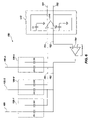
FIG. 8 illustrates an imaging system 300 including an semiconductor imager 40 containing a pixel column amplifier (not shown) according to the present invention. The imaging system 300 includes a processor 330 for receiving and modifying digital representations of images from the semiconductor imager 40. The imaging system 300 may also include an optical receiver 310 for channeling, focusing, or modifying incident energy 320, being visible light in one case, to present an optical image to the image sensor. For example, the optical receiver 310 may include a lens 315 for focusing the incident energy 320 onto the semiconductor imager 40.
The imaging system 300 may include a communication interface 360 for transmitting and receiving data. Finally, the imaging system 300 may include memory (340 and 350) in the form of local storage 340 and removable storage 350, such as, for example, Flash memory, magnetic recording media and optical recording media.
Without being limiting, such an imaging system 300 may include a computer system, camera system, scanner, machine vision, videophone, surveillance system, auto focus system, image stabilization system, and data compression system.
Although this invention has been described with reference to particular embodiments, the invention is not limited to these described embodiments. Rather, the invention is limited only by the appended claims, which include within their scope all equivalent devices or methods that operate according to the principles of the invention as described.