US7623235B2 - Curved grating spectrometer with very high wavelength resolution - Google Patents

Curved grating spectrometer with very high wavelength resolution Download PDF

Info

Publication number
US7623235B2
US7623235B2 US11/872,455 US87245507A US7623235B2 US 7623235 B2 US7623235 B2 US 7623235B2 US 87245507 A US87245507 A US 87245507A US 7623235 B2 US7623235 B2 US 7623235B2
Authority
US
United States
Prior art keywords
slit
grooves
grating
demultiplexer
wavelength
Prior art date
Legal status (The legal status is an assumption and is not a legal conclusion. Google has not performed a legal analysis and makes no representation as to the accuracy of the status listed.)
Expired - Lifetime, expires
Application number
US11/872,455
Other versions
US20080285919A1 (en
Inventor
Seng-Tiong Ho
Seongsik Chang
Yingyan Huang
Current Assignee (The listed assignees may be inaccurate. Google has not performed a legal analysis and makes no representation or warranty as to the accuracy of the list.)
Individual
Original Assignee
Individual
Priority date (The priority date is an assumption and is not a legal conclusion. Google has not performed a legal analysis and makes no representation as to the accuracy of the date listed.)
Filing date
Publication date
Priority claimed from US10/708,730 external-priority patent/US7283233B1/en
Application filed by Individual filed Critical Individual
Priority to US11/872,455 priority Critical patent/US7623235B2/en
Assigned to HO, SENG-TIONG reassignment HO, SENG-TIONG ASSIGNMENT OF ASSIGNORS INTEREST (SEE DOCUMENT FOR DETAILS). Assignors: HUANG, YINGYAN, CHANG, SEONGSIK
Publication of US20080285919A1 publication Critical patent/US20080285919A1/en
Priority to US12/623,750 priority patent/US8462338B1/en
Application granted granted Critical
Publication of US7623235B2 publication Critical patent/US7623235B2/en
Priority to US13/911,847 priority patent/US8854620B2/en
Priority to US14/482,615 priority patent/US9612155B2/en
Adjusted expiration legal-status Critical
Expired - Lifetime legal-status Critical Current

Links

Images

Classifications

    • GPHYSICS
    • G01MEASURING; TESTING
    • G01JMEASUREMENT OF INTENSITY, VELOCITY, SPECTRAL CONTENT, POLARISATION, PHASE OR PULSE CHARACTERISTICS OF INFRARED, VISIBLE OR ULTRAVIOLET LIGHT; COLORIMETRY; RADIATION PYROMETRY
    • G01J3/00Spectrometry; Spectrophotometry; Monochromators; Measuring colours
    • G01J3/12Generating the spectrum; Monochromators
    • G01J3/18Generating the spectrum; Monochromators using diffraction elements, e.g. grating
    • G01J3/20Rowland circle spectrometers
    • GPHYSICS
    • G01MEASURING; TESTING
    • G01JMEASUREMENT OF INTENSITY, VELOCITY, SPECTRAL CONTENT, POLARISATION, PHASE OR PULSE CHARACTERISTICS OF INFRARED, VISIBLE OR ULTRAVIOLET LIGHT; COLORIMETRY; RADIATION PYROMETRY
    • G01J3/00Spectrometry; Spectrophotometry; Monochromators; Measuring colours
    • G01J3/12Generating the spectrum; Monochromators
    • G01J3/18Generating the spectrum; Monochromators using diffraction elements, e.g. grating
    • G01J3/22Littrow mirror spectrometers

Definitions

  • the present invention relates to semiconductor photonic and opto-electronic devices.
  • the present invention relates to an integrated optical wavelength multiplexers and demultiplexers and method of making the same.
  • Optical gratings are well known in the art and are used to disperse optical spectra spatially. Such gratings are commonly used in optical spectrometers to analyze the spectra composition of an optical beam. There is always a trade off between the length of an optical spectrometer and its resolution. Thus, if a higher wavelength resolution is required, the length required is also longer.
  • RS the relative resolution vs size
  • RS basically measures the compactness of a spectrometer for a given resolution power. The smaller the RS value, the more compact is the spectrometer. Only a few conventional spectrometers have RS factor less than about 10. This is primarily because of the various limitations in the current art (as will be described below).
  • FIG. 1A The schematics of such a grating spectrometer is shown in FIG. 1A , illustrating an optical beam 1 entering an entrance slit 2 with slit size w 1 .
  • the beam after slit 2 , undergoes wave diffraction towards a curved grating 3 , which diffracts the beam spatially in a direction that is dependent on the optical wavelength of the beam.
  • the curvature of the grating helps to refocus the diffracted beam to an exit slit 4 with slit size w 2 .
  • Light through slit 4 is then detected by a photo detector 5 .
  • the commonly used design for the curved grating 3 is the Rowland design.
  • the grating has a circularly curved shape of radius R 6 and the slits SL 1 and SL 2 lie in a circle of radius R/2 7 as shown in FIG. 1A .
  • the grating is ruled using a diamond tip with constant horizontal displacement d, which ruled the curved surface with constant Chord lines C 1 , C 2 , C 3 and so forth, as shown in FIG. 1B .
  • the segment lengths, S 1 , S 2 , S 3 and so forth, along the curved surface are not a constant and vary along the curved surface.
  • ⁇ div 2 ⁇ /d (in Radian).
  • L the distance between the grating center and entrance slit 1 , which is also approximately the distance between the grating center and the exit slit 4 .
  • the resolution of the spectrometer increases with decreasing slit size w 2 .
  • the imaging through the curved grating requires w 1 and w 2 to be about equal.
  • a smaller slit size w 1 and w 2 to be about equal.
  • a smaller slit size w 1 leads to a larger diffraction angle ⁇ div .
  • FIG. 1C illustrating the ray tracing for the typical Rolwand-Echelle design at 4, 8, and 16 DEG diffraction.
  • the ray tracing will allow us to see potential focusing distortion or aberration at the exit slit.
  • a curved-grating spectrometer is well specified by geometric configurations of its components as shown in FIG. 2 .
  • the location of the entrance slit this is usually given by an ⁇ 1 with respect to the normal of the grating center and the distance S 1 from the grating center.
  • the center of the grating refers to the part of the grating hit by the center, i.e. high intensity point, of the entrance beam.
  • and d ⁇ 1
  • a circle can be defined by these three points X 0 , X 1 , and X 2 and its radius is referred to as the radius is referred to as the radius of curvature at the grating center.
  • the location of the exit slit i.e. the location of the detector; this is specified by an angle ⁇ 2 with respect to the normal of the grating center and the distance S 2 from the grating center.
  • the initial groove spacing d is usually chosen to satisfy the diffraction grating formula for a given entrance slit and detector location.
  • the locus of all the groove X ( ⁇ N) , . . . , X ( ⁇ 1) , X 0 , X 1 , . . . , X N form a curved shape, which can lie in a circle or in any other curvilinear line. Curved shape of the grating acts as an imaging element of the spectrometer.
  • each groove centered at X i is not critical to the resolution power of the grating and hence is not necessary to be a part of the main specification.
  • the groove shape is related to the diffraction efficiency.
  • it is typically made a planar surface for each groove, oriented in such a way that it acts like a tiny mirror reflecting the input ray towards the angle ⁇ 2 , a process typically referred to as blazing to angle ⁇ 2 (for a given wavelength ⁇ ).
  • a section of each groove which reflects light is physically a two-dimensional surface of a particular shape, not a one-dimensional curve.
  • the geometric shape of a groove is usually referred to as a curve of a particular shape. This is because there is no variation in the grating shape in the direction perpendicular to the plane where grating lies.
  • spectrometers within a planar waveguide are strictly two-dimensional in their nature and the shape of grating or grooves will be referred with a curve, not with surface.
  • the entrance slit is located on a circle of R/2, where R is the radius of curvature at the grating center.
  • This circle of radius R/2 is called as Rowland circle and it is tangent to the grating center.
  • the detector is also located on the same Rowland circle as the entrance slit.
  • All other grooves specified by its position vector X 1 's, are located on the same circle of radius R defined by the initial three groove positions X, X, and X ⁇ 1 .
  • X 1 's are also equally spaced along a chord that is parallel to the tangent of the grating center. In other words, the projection of the displacement vector X 1 ⁇ X i ⁇ 1 on this chord always has the same length.
  • the Rowland circle where the entrance slit and the detector are located, has the radius of 50 ⁇ m.
  • the entrance slit is located at ( ⁇ 50, 50). It is well-known that grating is more efficient if the propagation direction of the diffracted light from the grating is parallel and opposite to the propagation direction of the input beam. Such a scheme is known as Littrow configuration and is widely used for a high-efficiency spectrometer. A Littrow configuration in the Rowland design will be equivalent to having the angle of detector being almost equal to the angle of the entrance slit, i.e., ⁇ 1 ⁇ 2 . In order to have Littrow configuration, the groove spacing d at the grating center has to be properly chosen so that it satisfies grating formula Eq. 1.
  • the detector location can be fine tuned by changing the initial groove spacing d. Lower the groove spacing d, larger the detector angle ⁇ 2 .
  • Achieving a smaller RS factor is important for combining or integrating high-resolution grating spectrometers with various photonic devices (such as lasers, modulators, or detectors in a compact module or silica/silicon/semiconductor wafer).
  • WDM wave-length-division-multiplexed
  • the costs of these integrated WDM devices are typically proportional to their sizes.
  • the wavelength dispersion elements such as the grating spectrometer or other form of wavelength filters, are typically about 100 times larger in size than any other photonic devices in the module or wafer. In order to reduce their costs substantially, it is desirable to reduce the size of these wavelength dispersion elements to as small a size as possible.
  • grating based spectrometers that have an RS factor of less than 10. It is also desirable to reduce the size, and hence the cost, of integrated WDM devices that are used in DWDM networks.
  • the present invention discloses such a device and a method for making the same.
  • a compact curved grating and associated compact curved grating spectrometer or wavelength Mux/deMux with integration possibility includes an entrance slit, a detector and a curved grating and the compact curved grating wavelength Mux/deMux with integration possibility includes at least an input slit or waveguide and at least an output slit or waveguide for propagating through at least an input light beam and at least an output light beam, respectively.
  • the locations of the entrance slit and the detector or the input slit (or waveguide) and the output slit (or waveguide) can be adjusted to control the performance of the spectrometer or wavelength Mux/deMux.
  • the distance between the grooves of the gratings depend on the location of the entrance slit or the input slit (or waveguide), the detector or the output slit (or waveguide), the center of the operation wavelength, the diffraction order and the refractive index of the medium.
  • FIG. 1A and FIG. 1B show different views of a curved grating having the Rowland design
  • FIG. 1C shows ray-tracing for a Rowland grating design indicating focusing distortion or aberration at the exit slit for the cases where the input divergence angles are 4 DEG (left), 8 DEG (middle), and 16 DEG (right);
  • FIG. 2 shows the general specification of a curved-grating spectrometer;
  • FIG. 3 illustrates the Rowland configuration specification for a Rowland curved grating;
  • FIG. 4 shows a specific case of Rowland design curved grating
  • FIG. 5A describes the Comparison of angular resolution for Rowland gratin (left) with input divergence angle 16DEG and the HR-CCG design with large-angle aberration correction at input divergence angle 50DEG (right);
  • FIG. 5B describes High Resolution Compact Curved Gratin specifications in accordance with a preferred embodiment of the present invention
  • FIG. 6 illustrates an example of High Resolution Compact Curved Grating with constant angle
  • FIG. 7 shows a High Resolution Compact Curved Grating with Constant Arc, the detector and the entrance slit being present on a tangent circle, in accordance with an embodiment of the present invention
  • FIGS. 8A and 8B show a comparison between the Rowland design and the High Resolution Compact Curved Grating with constant groove (arc) length in accordance with the present invention.
  • FIG. 9 illustrates a block diagram of a wavelength demultiplexor and a wavelength multiplexor.
  • FIG. 10 illustrates a curved grating spectrometer configured as a wavelength multiplexor.
  • FIG. 11 illustrates a curved grating spectrometer configured as a wavelength multiplexor.
  • FIG. 12 illustrates a curved grating spectrometer configured as a wavelength multiplexor/demultiplexor.
  • FIG. 13 illustrates a wavelength spectrometer configured as a multiplexor/demultiplexor with waveguides.
  • FIG. 14 illustrates a high resolution compact curved grating.
  • the present invention discloses a system comprising a compact curved grating (CCG), it associated compact curved grating spectrometer (CCGS) or wavelength Mux/deMux (WMDM) module and a method for making the same.
  • the system is capable of achieving very small (resolution vs. size) RS factor.
  • CCGS or WMDM module include an isolated optical spectrometer or wavelength Mux/deMux using discrete optical components such as slits, grating, spectrometer or wavelength Mux/deMux casing, detector, detector array, and motor drive. More generally, the CCGS or WMDM module could also be used as a wavelength dispersion element in a photonic integrated circuit.
  • the photonic integrated circuit can be based on either of glass (silica) waveguide, semiconductor waveguide (including but not limited to, polymer waveguide, or any other type of optical waveguiding devices.
  • Semiconductor waveguides include silicon or compound semiconductor waveguides such as III-V (GaAs, InP etc).
  • the wavelength dispersion element based on the CCGS or WMDM module in the photonic integrated circuit can be integrated with optical detector, laser, amplifier, modulator, splitter, multimode interference devices, other wavelength filters, array-waveguide-based devices, and other photonic devices, materials, or components to achieve a multi-component photonic integrated circuit with useful functionalities.
  • the CCG explained below is a High Resolution Compact Curved Grating (HR-CCG) that tries to alleviate the disadvantages associated with prior art mentioned earlier, by providing a high resolution in a small (compact) module.
  • HR-CCG High Resolution Compact Curved Grating
  • a wavelength demultiplexer (wavelength deMux) 100 is a device in which multiple wavelengths in a beam of light 112 are separated into several different beams of light 114 .
  • a wavelength multiplexer (wavelength Mux) 110 is a device in which multiple wavelengths in several beams of light 114 are combined to a single beam of light 112 .
  • a curved grating spectrometer functions as a wavelength deMux 100 if it has an input slit 116 at the input beam 112 location so that the multiple wavelengths in the input beam will be diffracted to several output points 114 and several output slits 118 are placed at the locations of the spectrometer detectors mentioned above at these output points to form several output beams each with a different wavelength.
  • the output slits 118 replace the detectors so that no detectors will be used.
  • a curved grating spectrometer functions as a wavelength Mux 110 if it has multiple input slits 116 , each slit placed at an input beam's 114 location so that all the input beams 114 will be diffracted to the same output point and an output slit 118 is placed at the location of the spectrometer detector mentioned above so that the output slit 118 will give a single output beam of light 112 with the combined wavelengths of light.
  • the output slit 118 replaced the detector so that no detector will then be used.
  • a more general wavelength Mux/deMux device 120 will have multiple input slits 116 and multiple output slits so that several input beams of light 122 , each input beam with one or more wavelengths, are dispersed to form several output beams of light 124 , each output beam with one or several wavelengths.
  • an integrated version of the wavelength Mux/deMux device 130 will use optical waveguides 132 replacing input and output slits in which the mouth of each waveguide 132 will be at the location of the slit it is replacing.
  • the waveguides 132 can be formed by optical fibers or with multiple-layer dielectric materials with high-refractive-index core to guide optical waves in the form of channel or planar waveguides 132 .
  • Such channel or planar waveguides can be formed on a common substrate 132 .
  • the location of entrance slit or input slit (or waveguide) 502 can be adjusted in order to have the best performance for a particular design goal.
  • the location of a entrance slit 502 specified by angle ⁇ 1 with respect to the normal of grating center 504 and the distance S 1 from grating center 504 is not necessarily on a circle as in the case for Rowland design mentioned in the prior art.
  • the location of detector or output slit (or waveguide) can be adjusted in order to have the best performance for a particular design goal.
  • the location of detector or output slit (or waveguide) 506 specified by the angle ⁇ 2 with respect to the normal of grating center 504 and the distance S 2 from the grating center is not necessarily on the same circle where entrance slit or input slit (or waveguide) 502 is located, nor on any other circle.
  • n is the refractive index of the medium
  • ⁇ c is the center of the operation wavelength
  • d 1 ( ⁇ 1 ,S 1 ,X i ) is the distance from a i-th groove located at X i to entrance slit 502 specified by ⁇ 1 and S 1
  • d 2 ( ⁇ 2 ,S 2 ,X i ) is the distance from i-th groove located X i to detector 502 specified by ⁇ 2 and S 2
  • m is the diffraction order
  • n is the refractive index of the medium.
  • the second of these conditions being specific for a particular design goal of a curved-grating spectrometer.
  • the unknown real variables in both equations (2) and (3) are x- and y-coordinates of the location vector X i of the i-th groove.
  • the unknown real variables in both equations (2) and (3) are x- and y-coordinates of the location vector X i of the i-th groove.
  • the last of the HR-CCG specification ensures that every ray from each groove focuses to a single point. This ensures HR-CCG having a large acceptance angle, and therefore a small spot size.
  • FIG. 6 An exemplary embodiment of HR-CCG specified above is shown in FIG. 6 .
  • entrance slit 502 and detector 506 is not located on a circle tangent to the grating center.
  • Other groove locations X i 's are obtained with the condition of each groove having a constant angular spacing from entrance slit 502 and optical path-difference condition (Eq. 2). In a mathematical form, this condition is expressed as,
  • X in ( ⁇ S 1 ⁇ sin ⁇ 1 , S 1 ⁇ cos ⁇ 1) is the position vector of entrance slit 502
  • X det ( ⁇ S 2 ⁇ sin ⁇ 2 , S 2 ⁇ cos ⁇ 2 ) is the position vector of detector 506
  • ⁇ i is the difference in angular position between successive i th and (i ⁇ 1) th grooves.
  • operator “ ⁇ ” means the inner product in vector analysis and defined as A ⁇ B ⁇
  • ⁇ ⁇ ⁇ ⁇ 1 arc ⁇ ⁇ cos ⁇ ( X 1 - X i ⁇ ⁇ n ) ⁇ ( X 0 - X i ⁇ ⁇ n ) ⁇ X 1 - X i ⁇ ⁇ n ⁇ ⁇ ⁇ X 0 - X i ⁇ ⁇ n ⁇
  • wave-font of the diverging input beam propagating toward the curved grating is sliced into a set of narrow beams with angular extension ⁇ by the curved-grating. Each beam with angular extension ⁇ undergoes reflective diffraction by each groove.
  • diffraction at a particular groove is equivalent to redirecting to a particular narrow beam into a detector 506 location with ⁇ 2 .
  • the position vectors X i 's calculated from Eq. (2) and Eq. (4) are listed in the Table 2. As shown in FIG. 6 , the positions of grooves X i are not on a circle tangent to grating.
  • the High-Resolution Compact Curved Grating has Constant Arc and the Detector or output slit (or waveguide) is located on a tangent Circle. This embodiment is described below in detail.
  • both entrance slit or input slit (or waveguide) 502 and detector or output slit (or waveguide) 506 are located on a circle tangent to the grating center as in the case of Rowland design mentioned earlier.
  • grooves in this curved-grating are located such that the arc-length of each groove is the same. As a result, grooves are not located on a circle nor are spaced with equal distance.
  • elliptic shape is used for each groove and the length of this elliptic shape in each groove is kept constant. Center positions of the grooves X i 's in this example are determined so that the length of each elliptic groove is the same.
  • the location of other grooves X i 's are obtained by the following two conditions.
  • ⁇ ⁇ ⁇ S i ⁇ X i - X i ⁇ ⁇ n ⁇ ⁇ arccos ⁇ ( X i - 1 + X i 2 - X i ⁇ ⁇ n ) ⁇ ( X i + X i + 1 2 - X i ⁇ ⁇ n ) ⁇ X i - 1 + X i 2 - X i
  • FIG. 7 shows a specific example of the HR-CCG with constant arc-length of the grooves and detector or output slit (or waveguide) 506 at a tangent circle.
  • Both entrance slit or input slit (or waveguide) 502 and exit slit or output slit (and waveguide) 506 are located on a tangent circle of radius 50 ⁇ m.
  • the performance of the HR-CCG with the constant arc-length and detector on a tangent circle is compared with a Rowland design with the same parameters such as ⁇ 1 , S 1 , ⁇ 2 , S 2 , R, m, d, and ⁇ c . It is a direct comparison of a Rowland curved-grating spectrometer described in FIG. 3 and a HRC-curved grating spectrometer described in FIG. 7 . All the configuration parameters are the same for these two spectrometers except the grating itself. Particularly, the imaging properties, that is, how well entrance slit or input slit (or waveguide) 502 is sharply imaged at the detector location without aberration are compared.
  • Imaging properties ultimately determine the resolution of a spectrometer Finite Difference Time Domain (FDTD) method is used as a calculation method.
  • FDTD Finite Difference Time Domain
  • FDTD is a Maxwell-equation solver, which evaluates electromagnetic wave within a spatial region for a certain period of time. By choosing a fine spatial grid size and temporal calculation step, the equation for an electromagnetic wave and its propagation can be solved with arbitrarily fine resolution.
  • Imaging properties in these two curved-grating spectrometers is calculated by propagating a monochromatic light into entrance slit or input slit (or waveguide) 502 of each spectrometer.
  • FDTD is run until the interference of beams from the entire grating groove is completed and forms an image of entrance slit or input slit (or waveguide) 502 at the detector location.
  • the resulting snapshot of electric-field near the detector is taken for these two cases as shown in FIG. 8 .
  • FIG. 8A shows the snapshot of electric field at the detector location for the Rowland design described in FIG. 3 .
  • the image of the entrance slit is blurred due to imperfect grating.
  • FIG. 8B shows the snapshot of electric field for the HR-CCG with constant arc-length grooves and detector on a tangent circle. In this case, a sharp aberration free image of entrance slit is formed at the detector location.
  • High-Resolution Compact Curved Grating has a constant arc with the detector or output slit (or waveguide) being present in-line. With reference to FIG. 7 , this embodiment can be realized if the input and exit slits are located along a line such that S 1 ⁇ S 2 . In another alternate embodiment, High-Resolution Compact Curved Grating has a constant arc with detector or output slit (or waveguide) 506 present at an arbitrary location.
  • High-Resolution Compact Curved Grating has a constant angle and detector 506 present on the circle of radius R, as depicted in FIG. 6 .
  • each groove surface has an angular extension ( ⁇ ) i from entrance slit 502 .
  • the angular extensions ( ⁇ ) I are kept constant for all grooves.
  • both entrance slit 502 and detectors 506 are located on a circle of radius R/2, where R is the radius of a circle formed by three initial groove locations X 0 , X 1 , and X 2 .
  • High-Resolution Compact Curved Grating has a constant angle and detector or output slit (or waveguide) 506 is present on the circle of radius R/2, as depicted in FIG. 6 .
  • each groove surface has an angular extension ( ⁇ ) i from entrance slit or input slit (or waveguide) 502 .
  • the angular extensions ( ⁇ ) i are kept constant for all grooves.
  • both entrance slit or input slit (or waveguide) 502 and detectors or output slits (or waveguides) 506 are located on or near a circle of radius R/2, where R is the radius of a circle formed by three initial groove locations X 0 , X 1 , and X 2 .
  • High-Resolution Compact Curved Grating has a constant angle with detector or output slit (or waveguide) 506 present at an arbitrary location.
  • High-Resolution Compact Curved Grating has groves lying on or near the circle of radius R (the near-Rowland Case) where R is the radius of a circle formed by three initial groove locations X 0 , X 1 , and X 2 , and the detector or output slit (or waveguide) 506 is present on the circle of radius R/2, as depicted in FIG. 14 .
  • each groove surface has an angular extension ( ⁇ ) i from entrance slit or input slit (or waveguide).
  • the angular extensions ( ⁇ ) i are chosen so that each groove lies on or near the circle of radius R.
  • the location of other grooves X i 's are obtained by the following two conditions.
  • each groove is located at or near the circle of radius R throughout the HR-CCG, where R is the radius of a circle formed by three initial groove locations X 0 , X 1 , and X 2 .
  • the High-Resolution Compact Curved Grating with groves on or near the circle of radius R has detector or output slit (or waveguide) present at an arbitrary location.

Abstract

The present application discloses a system comprising a compact curved grating (CCG) and its associated compact curved grating spectrometer (CCGS) or compact curved grating wavelength multiplexer/demultiplexer (WMDM) module and a method for making the same. The system is capable of achieving a very small (resolution vs. size) RS factor. In the invention, the location of the entrance slit and detector can be adjusted in order to have the best performance for a particular design goal. The initial groove spacing is calculated using a prescribed formula dependent on operation wavelength. The location of the grooves is calculated based on two conditions. The first one being that the path-difference between adjacent grooves should be an integral multiple of the wavelength in the medium to achieve aberration-free grating focusing at the detector or output slit (or output waveguide) even with large beam diffraction angle from the entrance slit or input slit (or input waveguide). The second one being specific for a particular design goal of a curved-grating spectrometer. In an embodiment, elliptical mirrors each with focal points at the slit and detector are used for each groove to obtain aberration-free curved mirrors.

Description

CROSS REFERENCE TO RELATED APPLICATIONS
This application is a Continuation-In-Part of U.S. patent application Ser. No. 10/708,730, filed Mar. 20, 2004 now U.S. Pat. No. 7,283,233. This application is related to U.S. patent application Ser. No. 09/916,701, “Method for shifting bandgap energy of quantum well layer” filed Jul. 26, 2001 in the names of Boon-Siew Ooi and Seng-Tiong Ho, the disclosure of which is incorporated herein by reference. This application is related to U.S. Patent Application Ser. No. 60/242,219, “Method for shifting bandgap energy of quantum well layer” filed Oct. 20, 2000, in the names of Boon-Siew Ooi and Seng-Tiong Ho, the disclosure of which is incorporated herein by reference. This application is related to U.S. Patent Application Ser. No. 60/430,507, “Method for quantum-well intermixing using pre-annealing enhanced defect diffusion” filed Dec. 3, 2002, in the names of Boon-Siew Ooi and Ruiyu (Jane) Wang, the disclosure of which is incorporated herein by reference.
BACKGROUND OF THE INVENTION
The present invention relates to semiconductor photonic and opto-electronic devices. In particular, the present invention relates to an integrated optical wavelength multiplexers and demultiplexers and method of making the same.
Optical gratings are well known in the art and are used to disperse optical spectra spatially. Such gratings are commonly used in optical spectrometers to analyze the spectra composition of an optical beam. There is always a trade off between the length of an optical spectrometer and its resolution. Thus, if a higher wavelength resolution is required, the length required is also longer. Consider an example of a typical 1-meter long grating spectrometer in the market, which has a wavelength resolution of about Δλ=0.1 nm at λ=1000 nm or Δλ/λ=10−4. The dimensionless quantity for the length of the spectrometer L is L/λ and L/λ=106 in this example. The dimensionless product of the relative resolution Δλ/λ and the relative physical size L/λ of the spectrometer is dependent on the design of the spectrometer and in this example, spectrometer gives (Δλ/λ)×(L/λ)=100=RS. This factor (RS) in generally referred to as the “resolution vs size” factor. RS basically measures the compactness of a spectrometer for a given resolution power. The smaller the RS value, the more compact is the spectrometer. Only a few conventional spectrometers have RS factor less than about 10. This is primarily because of the various limitations in the current art (as will be described below).
It is known in the art that a relatively compact spectrometer can be achieved using a curved grating. The schematics of such a grating spectrometer is shown in FIG. 1A, illustrating an optical beam 1 entering an entrance slit 2 with slit size w1. The beam, after slit 2, undergoes wave diffraction towards a curved grating 3, which diffracts the beam spatially in a direction that is dependent on the optical wavelength of the beam. The curvature of the grating helps to refocus the diffracted beam to an exit slit 4 with slit size w2. Light through slit 4 is then detected by a photo detector 5. As is well known to those skilled in the art, the commonly used design for the curved grating 3 is the Rowland design. In the Rowland design, the grating has a circularly curved shape of radius R 6 and the slits SL1 and SL2 lie in a circle of radius R/2 7 as shown in FIG. 1A. The grating is ruled using a diamond tip with constant horizontal displacement d, which ruled the curved surface with constant Chord lines C1, C2, C3 and so forth, as shown in FIG. 1B. The segment lengths, S1, S2, S3 and so forth, along the curved surface are not a constant and vary along the curved surface.
Let the diffraction full angle from the entrance slit 1 be θdiv. As is well known to those skilled in the art, θdiv=2λ/d (in Radian). Let length L be the distance between the grating center and entrance slit 1, which is also approximately the distance between the grating center and the exit slit 4. as is well know to those skilled in the art, the resolution of the spectrometer increases with decreasing slit size w2. The imaging through the curved grating requires w1 and w2 to be about equal. a smaller slit size w1 and w2 to be about equal. A smaller slit size w1, however, leads to a larger diffraction angle θdiv. It can be shown that the Rowland design works reasonably well up to θdiv<4°. When θdiv>4°, the Rowland design could not give a sharp enough focus at the exit slit 4 (for Δλ<0.1 nm), thereby limiting the size of w2 and hence the resolution of the spectrometer. A diffraction angle of θdiv=4° corresponds to a slit size of about 25 microns (for λ=1000 nm). In the current art, it is typically difficult to make slit size smaller than 25 microns, and Rowland design is adequate for most present spectrometers with slit sizes larger than 25 microns.
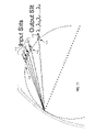
Aberration limitation. In the case of the Rowland design, when Θdiv>4 DEG, serous aberration in the refocusing beam will occur to limit wavelength resolution. This is shown in FIG. 1C illustrating the ray tracing for the typical Rolwand-Echelle design at 4, 8, and 16 DEG diffraction. The ray tracing will allow us to see potential focusing distortion or aberration at the exit slit. In the figure, we show the focusing behavior for two sets of rays with wavelengths separated by 0.4 nm. From the figure, we see that their focused spots clearly separate when Θdiv=4 DEG. However, when Θdiv=8 DEG, the focused spots began to smear out. There is substantial distortion for the focusing rays when Θdiv>4 DEG. Further simulations based on numerical solutions to Maxwell's wave equations using finite-difference time-domain (FDTD) method also show similar onset of focused spot size distortion at Θdiv>4 DEG. In short, the current designs are close to their resolution-size (RS) limits and cannot be made substantially more compact without losing wavelength resolution.
As discussed above, a curved-grating spectrometer is well specified by geometric configurations of its components as shown in FIG. 2. First, the location of the entrance slit; this is usually given by an θ1 with respect to the normal of the grating center and the distance S1 from the grating center. The center of the grating refers to the part of the grating hit by the center, i.e. high intensity point, of the entrance beam. Second, the locations of the first two grooves at the grating center; these are specified by its location vectors X1 and X(−1) with respect to the grating center X0=0 and its groove spacing (or pitch) d1=|X1−X0| and d−1=|X(−1)−X0|. X1 and X(−1) are located symmetrically opposite to each other with respect to the grating center and therefore d=d1=d(−1). A circle can be defined by these three points X0, X1, and X2 and its radius is referred to as the radius is referred to as the radius of curvature at the grating center. Third, the location of the exit slit i.e. the location of the detector; this is specified by an angle θ2 with respect to the normal of the grating center and the distance S2 from the grating center. For a given operating wavelength center λc, the initial groove spacing d is usually chosen to satisfy the diffraction grating formula for a given entrance slit and detector location. The curved grating is further specified by the location of other grooves (specified by its location vector Xi, with respect to the grating center X0=0 and the groove spacing di from the previous groove given by di=|XiXi−1|. Let the total number of groove be N in each side of the grating center, the locus of all the groove X(−N), . . . , X(−1), X0, X1, . . . , XN form a curved shape, which can lie in a circle or in any other curvilinear line. Curved shape of the grating acts as an imaging element of the spectrometer.
The shape of each groove centered at Xi is not critical to the resolution power of the grating and hence is not necessary to be a part of the main specification. However, the groove shape is related to the diffraction efficiency. For example, in order to increase the diffraction efficiency at a particular diffraction angle θ2, it is typically made a planar surface for each groove, oriented in such a way that it acts like a tiny mirror reflecting the input ray towards the angle θ2, a process typically referred to as blazing to angle θ2 (for a given wavelength λ). A section of each groove which reflects light is physically a two-dimensional surface of a particular shape, not a one-dimensional curve. However, the geometric shape of a groove is usually referred to as a curve of a particular shape. This is because there is no variation in the grating shape in the direction perpendicular to the plane where grating lies. Especially, spectrometers within a planar waveguide are strictly two-dimensional in their nature and the shape of grating or grooves will be referred with a curve, not with surface.
Conventional Rowland design spectrometers are specifically configured by the design rule described below in conjunction with FIG. 3.
Referring to FIG. 3, the entrance slit is located on a circle of R/2, where R is the radius of curvature at the grating center. This circle of radius R/2 is called as Rowland circle and it is tangent to the grating center. In the Rowland design, the distance S1 of the entrance slit to the grating center is related to the angle of incidence θ1 by S1=R×cosθ1.
The detector is also located on the same Rowland circle as the entrance slit. In the Rowland design, the distance S2 of the detector to the grating center is related to the angle of diffraction θ2 by S2=R×cosθ2.
The relation between θ1, θ2, and the initial groove spacing d is given by the grating formula,
d(sinΘ2−sinΘ1)= c /n  (1)
where m is the diffraction order, n is the refractive index of the medium, λc is the center of the operation wave-length. This grating formula is a so-called far-field approximation, which is valid only when S1 and S2 are much larger than d.
Initial groove positions are X0=(0,0), X1=(d, R−(R2−d2)1/2) and X−1=(−d, R−(R2−d2)1/2). These three initial grooves with position vectors X0, X1, and X−1, are located on a circle of radius R and have the initial groove spacing of d along a chord parallel to the grating tangent.
All other grooves, specified by its position vector X1's, are located on the same circle of radius R defined by the initial three groove positions X, X, and X−1. X1's are also equally spaced along a chord that is parallel to the tangent of the grating center. In other words, the projection of the displacement vector X1−Xi−1 on this chord always has the same length. Specifically, the position vectors of these grooves can be written as xi=(di, R−(R2−(di)2)1/2), and X−i=(di, R−(R2−(di)2)1/2.
For example, if the radius of curvature at the grating center is r=100 μm, the Rowland circle, where the entrance slit and the detector are located, has the radius of 50 μm. Here, we assume that tangent line at the grating center is parallel to the x-axis. Since the Rowland circle is tangent to the grating center, it circles by passing both the grating center X0=(0,0) and a point (0, 50). If the angle of the entrance slit is θ1=45°, the distance of the entrance slit to the grating center is S1=R×cosθ1=70.71 μm. In terms of (x,y)-coordinate, the entrance slit is located at (−50, 50). It is well-known that grating is more efficient if the propagation direction of the diffracted light from the grating is parallel and opposite to the propagation direction of the input beam. Such a scheme is known as Littrow configuration and is widely used for a high-efficiency spectrometer. A Littrow configuration in the Rowland design will be equivalent to having the angle of detector being almost equal to the angle of the entrance slit, i.e., θ1≈θ2. In order to have Littrow configuration, the groove spacing d at the grating center has to be properly chosen so that it satisfies grating formula Eq. 1. For example, when the center wavelength is 1550 nm and the angle of entrance slit is θ1=45°, the diffraction order of m=12 of a grating with the groove spacing of d=4.2 μm at its center propagate toward a detector located at θ2=37.37°, which is close to the Littrow configuration. The detector location can be fine tuned by changing the initial groove spacing d. Lower the groove spacing d, larger the detector angle θ2. For the groove spacing d=4.2 μm and radius of curvature R=100 μm, the initial three positions of grooves are X0=(0,0), X1=(4.2, 0.088) and X−1=(−4.2, 0.088).
In the Rowland design, other grooves are located such that their spacing is the same along a chord parallel to the grating tangent at the center. Therefore, the position vectors of other grooves are Xi=(di, R−(R2−(di)2)1/2)=(4.2i, 100−(1002−(4.2i)2)1/2), and X−i=(−di, R−(R2−(di)2)1/2)=(−4.2i, 100−(1002−(4.2i)2)1/2). The position vectors of the grooves are listed in the following table for the case of Rowland design with R=100 μm, d=4.2 μm, m=12, θ1=45°, and θ2=37.37° for an operation wavelength of λc=1550 nm.
TABLE 1
X−13 (−54.6, 16.221)
X−12 (−50.4, 13.630)
X−11 (−46.2, 11.312)
X−10 (−42, 9.248)
X−9 (−37.8, 7.419)
X−8 (−33.6, 5.814)
X−7 (−29.4, 4.419)
X−6 (−25.2, 3.227)
X−5 (−21, 2.230)
X−4 (−16.8, 1.421)
X−3 (−12.6, 0.797)
X−2 (−8.4, 0.353)
X−1 (−4.2, 0.088)
X0 (0, 0)
X1 (4.2, 0.088)
X2 (8.4, 0.353)
X3 (12.6, 0.797)
X4 (16.8, 1.421)
X5 (21, 2.230)
X6 (25.2, 3.227)
The advent in Dense Wavelength Division Multiplexing (DWDM) optical communication networks, however, requires that the multiple wavelengths in an optical fiber to be analyzed by spectral analysis devices that are much smaller in size than that of the current grating spectrometer. The challenge is to circumvent the current limitation in grating spectrometer design and fabrication methods. As discussed above, the current design basically cannot achieve the Resolution-Size factor (RS) much smaller than about 10. While several current technologies are capable of using planar waveguide technologies to make grating based spectrometers on a single silica or semiconductor substrate, they are still not able to achieve RS much smaller than 10 due to the basic limitations of the grating spectrometer design. Achieving a smaller RS factor is important for combining or integrating high-resolution grating spectrometers with various photonic devices (such as lasers, modulators, or detectors in a compact module or silica/silicon/semiconductor wafer).
These wave-length-division-multiplexed (WDM) integrated photonic devices or modules would be of great importance for applications to DWDM networks. The costs of these integrated WDM devices are typically proportional to their sizes. The wavelength dispersion elements, such as the grating spectrometer or other form of wavelength filters, are typically about 100 times larger in size than any other photonic devices in the module or wafer. In order to reduce their costs substantially, it is desirable to reduce the size of these wavelength dispersion elements to as small a size as possible.
Thus, it is desirable to have grating based spectrometers that have an RS factor of less than 10. It is also desirable to reduce the size, and hence the cost, of integrated WDM devices that are used in DWDM networks. The present invention discloses such a device and a method for making the same.
SUMMARY OF THE INVENTION
It is an aim of the invention to provide a compact curved grating and associated compact curved grating spectrometer or wavelength Mux/deMux with integration possibility that is capable of achieving very small RS factors thereby enabling high resolution at small size.
It is another aim of the invention to provide a compact curved grating spectrometer module that can be used as an isolated optical spectrometer using discrete optical spectrometer module or wavelength Mux/deMux module with integration possibility that can be used as an isolated optical spectrometer using discrete optical components.
It is another aim of the invention to provide a compact curved grating spectrometer module that can be used as a wavelength dispersion element in a photonic integrated circuit.
In order to attain the above-mentioned aims, a compact curved grating and associated compact curved grating spectrometer or wavelength Mux/deMux with integration possibility is provided. The compact curved grating spectrometer includes an entrance slit, a detector and a curved grating and the compact curved grating wavelength Mux/deMux with integration possibility includes at least an input slit or waveguide and at least an output slit or waveguide for propagating through at least an input light beam and at least an output light beam, respectively. The locations of the entrance slit and the detector or the input slit (or waveguide) and the output slit (or waveguide) can be adjusted to control the performance of the spectrometer or wavelength Mux/deMux. The distance between the grooves of the gratings depend on the location of the entrance slit or the input slit (or waveguide), the detector or the output slit (or waveguide), the center of the operation wavelength, the diffraction order and the refractive index of the medium.
BRIEF DESCRIPTION OF THE DRAWINGS
The preferred embodiments of the invention will hereinafter be described in conjunction with the appended drawings provided to illustrate and not to limit the invention, wherein like designations denote like elements, and in which FIG. 1A and FIG. 1B show different views of a curved grating having the Rowland design, and FIG. 1C shows ray-tracing for a Rowland grating design indicating focusing distortion or aberration at the exit slit for the cases where the input divergence angles are 4 DEG (left), 8 DEG (middle), and 16 DEG (right); FIG. 2 shows the general specification of a curved-grating spectrometer; FIG. 3 illustrates the Rowland configuration specification for a Rowland curved grating; FIG. 4 shows a specific case of Rowland design curved grating; FIG. 5A describes the Comparison of angular resolution for Rowland gratin (left) with input divergence angle 16DEG and the HR-CCG design with large-angle aberration correction at input divergence angle 50DEG (right); FIG. 5B describes High Resolution Compact Curved Gratin specifications in accordance with a preferred embodiment of the present invention; FIG. 6 illustrates an example of High Resolution Compact Curved Grating with constant angle; FIG. 7 shows a High Resolution Compact Curved Grating with Constant Arc, the detector and the entrance slit being present on a tangent circle, in accordance with an embodiment of the present invention; and FIGS. 8A and 8B show a comparison between the Rowland design and the High Resolution Compact Curved Grating with constant groove (arc) length in accordance with the present invention.
FIG. 9 illustrates a block diagram of a wavelength demultiplexor and a wavelength multiplexor.
FIG. 10 illustrates a curved grating spectrometer configured as a wavelength multiplexor.
FIG. 11 illustrates a curved grating spectrometer configured as a wavelength multiplexor.
FIG. 12 illustrates a curved grating spectrometer configured as a wavelength multiplexor/demultiplexor.
FIG. 13 illustrates a wavelength spectrometer configured as a multiplexor/demultiplexor with waveguides.
FIG. 14 illustrates a high resolution compact curved grating.
DETAILED DESCRIPTION
The present invention discloses a system comprising a compact curved grating (CCG), it associated compact curved grating spectrometer (CCGS) or wavelength Mux/deMux (WMDM) module and a method for making the same. The system is capable of achieving very small (resolution vs. size) RS factor. The uses of CCGS or WMDM module include an isolated optical spectrometer or wavelength Mux/deMux using discrete optical components such as slits, grating, spectrometer or wavelength Mux/deMux casing, detector, detector array, and motor drive. More generally, the CCGS or WMDM module could also be used as a wavelength dispersion element in a photonic integrated circuit. The photonic integrated circuit can be based on either of glass (silica) waveguide, semiconductor waveguide (including but not limited to, polymer waveguide, or any other type of optical waveguiding devices. Semiconductor waveguides include silicon or compound semiconductor waveguides such as III-V (GaAs, InP etc). The wavelength dispersion element based on the CCGS or WMDM module in the photonic integrated circuit can be integrated with optical detector, laser, amplifier, modulator, splitter, multimode interference devices, other wavelength filters, array-waveguide-based devices, and other photonic devices, materials, or components to achieve a multi-component photonic integrated circuit with useful functionalities. The CCG explained below is a High Resolution Compact Curved Grating (HR-CCG) that tries to alleviate the disadvantages associated with prior art mentioned earlier, by providing a high resolution in a small (compact) module.
We have improved on the current Rowland design, enabling curved-grating spectrometer with 10-100× smaller linear size (or 100-10,000× smaller area) using our HR-CCG with large-angle aberration-corrected design. The typical Rowland design can only reach a useful diffraction angle Θdiff of ˜4 DEG, beyond which serous aberration in the refocusing beam will occur to limit wavelength resolution. In FIG. 5A we show the angular resolution of the typical Rowland design at 16 DEG diffraction angle compared with our HR-CCG design at 50 DEG. We see that our “large-angle aberration-corrected grating” design has much better angular resolution: different direction rays are well converged to a point on the focal circle. This translates to much smaller RS factor or size. We have used discrete time solution of vectorial Maxwell's equations to simulate the HR-CCG design, which verified the high resolution nature of our grating as predicted by the ray-tracing method.
Referring to FIG. 9, a wavelength demultiplexer (wavelength deMux) 100 is a device in which multiple wavelengths in a beam of light 112 are separated into several different beams of light 114. A wavelength multiplexer (wavelength Mux) 110 is a device in which multiple wavelengths in several beams of light 114 are combined to a single beam of light 112.
Referring to FIG. 10 a curved grating spectrometer functions as a wavelength deMux 100 if it has an input slit 116 at the input beam 112 location so that the multiple wavelengths in the input beam will be diffracted to several output points 114 and several output slits 118 are placed at the locations of the spectrometer detectors mentioned above at these output points to form several output beams each with a different wavelength. The output slits 118 replace the detectors so that no detectors will be used.
Referring to FIG. 11, a curved grating spectrometer functions as a wavelength Mux 110 if it has multiple input slits 116, each slit placed at an input beam's 114 location so that all the input beams 114 will be diffracted to the same output point and an output slit 118 is placed at the location of the spectrometer detector mentioned above so that the output slit 118 will give a single output beam of light 112 with the combined wavelengths of light. The output slit 118 replaced the detector so that no detector will then be used.
Referring to FIG. 12, a more general wavelength Mux/deMux device 120 will have multiple input slits 116 and multiple output slits so that several input beams of light 122, each input beam with one or more wavelengths, are dispersed to form several output beams of light 124, each output beam with one or several wavelengths.
Referring to FIG. 13, an integrated version of the wavelength Mux/deMux device 130 will use optical waveguides 132 replacing input and output slits in which the mouth of each waveguide 132 will be at the location of the slit it is replacing. As is known to those skilled in the art, the waveguides 132 can be formed by optical fibers or with multiple-layer dielectric materials with high-refractive-index core to guide optical waves in the form of channel or planar waveguides 132. Such channel or planar waveguides can be formed on a common substrate 132.
First, the location of entrance slit or input slit (or waveguide) 502 can be adjusted in order to have the best performance for a particular design goal. Thus, the location of a entrance slit 502 specified by angle θ1 with respect to the normal of grating center 504 and the distance S1 from grating center 504 is not necessarily on a circle as in the case for Rowland design mentioned in the prior art.
Second, the location of detector or output slit (or waveguide) can be adjusted in order to have the best performance for a particular design goal. Thus, the location of detector or output slit (or waveguide) 506, specified by the angle θ2 with respect to the normal of grating center 504 and the distance S2 from the grating center is not necessarily on the same circle where entrance slit or input slit (or waveguide) 502 is located, nor on any other circle.
Third, The relation between θ1, θ2, and the initial groove spacing d is given by the grating formula,
d(sinΘ2−sinΘ1)= c /n  (1)
where m is the diffraction order, n is the refractive index of the medium, and λc is the center of the operation wavelength.
Fourth, the initial groove positions are X0=(0,0), X1=(d, R−(R2−d2)1/2) and X−1=(−d, R−(R2−d2)1/2) With these position vectors, three initial grooves are located on a circle radius R and have the initial groove spacing of d at the grating center.
Fifth, location of other grooves Xi's are obtained by two conditions. The first of these conditions being that the path-difference between adjacent grooves should be an integral multiple of the wavelength in the medium. The first condition can be expressed mathematically by:
[d 11 ,S 1 ,X 1)+d 22 ,S 2 ,X i)]−[d 11 ,S 1 ,X i−1)+d 22 ,S 2 ,X i−1)]=mλ/n,  (2)
(2)
where d11,S1,Xi) is the distance from a i-th groove located at Xi to entrance slit 502 specified by Θ1 and S1, d2 2,S2,Xi) is the distance from i-th groove located Xi to detector 502 specified by Θ2 and S2, m is the diffraction order, and n is the refractive index of the medium. This mathematical expression is numerically exact for the optical path difference requirement in the diffraction grating and is actively adjusted for every groove on HR-CCG.
The second of these conditions being specific for a particular design goal of a curved-grating spectrometer. The second condition in general can be mathematically expressed as
f1 ,S 12 ,X i ,X i−1c ,n,m)=const  (3)
Specific examples of the second condition are described later in the application. The unknown real variables in both equations (2) and (3) are x- and y-coordinates of the location vector Xi of the i-th groove. For given input-slit location (θ1, S1), detector 506 location (θ2, S2), and the previous, i.e., (i−1)-th, groove position Xi−1, Xi is completely specified by equations 3 and 4 for a given center wave-length λc, refractive index n, and the diffraction order m.
The last of the HR-CCG specification ensures that every ray from each groove focuses to a single point. This ensures HR-CCG having a large acceptance angle, and therefore a small spot size.
An exemplary embodiment of HR-CCG specified above is shown in FIG. 6. The radius of curvature at the grating center is R=50 μm. Entrance slit or input slit (or waveguide) 502 is located at an angle Θ1=55° from the grating normal and distance S1=28.68 μm from the grating center. Detector or output slit (or waveguide) 506 is located at an angle Θ2=27.2° the grating normal and distance S2=37.65 μm from the grating center. The groove spacing at the grating center is chosen to be d=3.6 μm so that diffraction order m=10 is directed toward detector 506 located at Θ2. As shown in FIG. 6, entrance slit 502 and detector 506 is not located on a circle tangent to the grating center. Three initial grooves are located at X0=(0, 0), X1=(3.6, 0.13), and X−1=(−3.6, 0.13) which form a circle radius R=50 μm. Other groove locations Xi's are obtained with the condition of each groove having a constant angular spacing from entrance slit 502 and optical path-difference condition (Eq. 2). In a mathematical form, this condition is expressed as,
cos ( Δ θ i ) = ( X i - X i n ) · ( X i - 1 - X i n ) X i - X i n X i - 1 - X i n = const ( 4 )
where Xin=(−S1·sinθ1, S1·cosθ1) is the position vector of entrance slit 502, Xdet=(−S2·sinθ2, S2·cosθ2) is the position vector of detector 506, and Δθi is the difference in angular position between successive ith and (i−1)th grooves. In Eq. 4, operator “·” means the inner product in vector analysis and defined as A·B≡|A||B| cosθ. Because Δθi is constant for all grooves, it is same as the angular −position difference between the center groove at X0 and the first groove at X1, i.e.
Δ θ 1 = arc cos ( X 1 - X i n ) · ( X 0 - X i n ) X 1 - X i n X 0 - X i n
In this particular case, the position of entrance slit or input slit (or waveguide) 502, exit slit or output slit (or waveguide) 506 and the angular spacing between the grooves are Xin=(−23.49, 16.45), Xdet=(−17.26, 33.46), and ΔΘ1=4.13°. In this example, wave-font of the diverging input beam propagating toward the curved grating is sliced into a set of narrow beams with angular extension ΔΘ by the curved-grating. Each beam with angular extension ΔΘ undergoes reflective diffraction by each groove. At a particular wavelength, diffraction at a particular groove is equivalent to redirecting to a particular narrow beam into a detector 506 location with Θ2. The position vectors Xi's calculated from Eq. (2) and Eq. (4) are listed in the Table 2. As shown in FIG. 6, the positions of grooves Xi are not on a circle tangent to grating.
X−10 (−23.17, 15.28)
X−9 (−22.24, 12.89)
X−8 (−20.97, 10.60)
X−7 (−19.36, 8.43)
X−6 (−17.42, 6.44)
X−5 (−15.17, 4.65)
X−4 (−12.62, 3.10)
X−3 (−9.80, 1.83)
X−2 (−6.74, 0.87)
X−1 (−3.60, 0.14)
X0 (0.00, 0.00)
X1 (3.60, 0.14)
X2 (7.30, 0.70)
X3 (11.06, 1.70)
X4 (14.83, 3.13)
X5 (18.57, 5.02)
X6 (22.22, 7.36)
X7 (25.73, 10.16)
X8 (29.06, 13.39)
X9 (32.16, 17.06)
X10 (34.98, 21.15)
The above example has been used for illustration purposes only and should not be construed in any way as limiting the scope of the invention.
In an alternative embodiment, the High-Resolution Compact Curved Grating has Constant Arc and the Detector or output slit (or waveguide) is located on a tangent Circle. This embodiment is described below in detail.
In this exemplary embodiment, both entrance slit or input slit (or waveguide) 502 and detector or output slit (or waveguide) 506 are located on a circle tangent to the grating center as in the case of Rowland design mentioned earlier. However, grooves in this curved-grating are located such that the arc-length of each groove is the same. As a result, grooves are not located on a circle nor are spaced with equal distance.
There are two commonly used shapes of grooves in the grating used in the free-space spectrometer. They are straight line and sinusoidal shape. These two shapes are widely used because of ease of manufacturing process. For a curved-grating, ideal shape of reflecting surface not a straight line, but a curved shape of the reflecting surface not a straight line, but a curved shape that can image entrance slit 502 at detector 506 location. Ideal aberration-free curved mirror is an ellipse with its focal point located at source and image. Therefore, the ideal shape of the groove in a curved-grating is a section of ellipse with its focal points at the slit and the detector. In this embodiment, elliptic shape is used for each groove and the length of this elliptic shape in each groove is kept constant. Center positions of the grooves Xi's in this example are determined so that the length of each elliptic groove is the same.
The geometric specification of the HR-CCG with constant arc-length and detector 506 at a tangent circle is as described below.
First, entrance slit or input slit (or waveguide) 502 is located on a circle tangent to the grating at its center (so-called tangent circle). Therefore, the angle θ1 and the distance S1 of entrance slit or input slit (or waveguide) 502 with respect to the grating center is related by S1=R cosθ1, where R is the radius of curvature of the grating center.
Third, the relation between Θ1, Θ2, and the initial grove spacing d is given by the grating formula, d(sinΘ2−sinΘ1)=mλc/n where m is the diffraction order, n is the refractive index of the medium, and λc is the center of the operation wavelength.
Fourth, initial groove positions are X0 (0,0), X1=(d, R−(R2−d2)1/2) and X−1=(−d, R−(R2−d2)1/2) With these position vectors, three initial grooves are located on a circle of radius R and have the initial groove spacing of d at the grating center.
Fifth, the location of other grooves Xi's are obtained by the following two conditions. The first condition being the path-difference between adjacent grooves should be an integral multiple of the wavelength in the medium, which s mathematically expressed as
[d 11 ,S 1 ,X i)+d 22 ,S 2 ,X i)]−[Θ1 ,S 1 ,X i−1)+d 22 ,S 2 ,X i−1)]=mλ/n  (2)
The arc-lengths of all the grooves are the same through-out the HR-CCG. This condition can be mathematically expressed as
Δ S i = X i - X i n arccos ( X i - 1 + X i 2 - X i n ) · ( X i + X i + 1 2 - X i n ) X i - 1 + X i 2 - X i | X i + X i + 1 2 - X i n ( 5 )
where ΔSi is the arc-length of ith groove. This equation requires the knowledge of Xi+1, which is still unknown. However, with the constraint the fact that each Xi is located at the center of the groove, the above expression can be reduced to the following expression without Xi+1.
Δ S i = 2 X i - X i n arc cos ( X i - 1 + X i 2 - X i n ) · ( X i - X i n ) X i - 1 + X i 2 - X i n X i - X i n = consi ( 6 )
FIG. 7 shows a specific example of the HR-CCG with constant arc-length of the grooves and detector or output slit (or waveguide) 506 at a tangent circle. The radius of curvature at the grating center is R=100 μm. Entrance slit or input slit (or waveguide) 502 is located at an angle Θ1=45° from grating normal and a distance S1=70.71 μm from the grating center. Detector 506 is located at an angle Θ2 37.37° and distance S2=79.47 μm from the grating center. Both entrance slit or input slit (or waveguide) 502 and exit slit or output slit (and waveguide) 506 are located on a tangent circle of radius 50 μm. The groove spacing at the grating center is chosen to be d=4.2 μm so that diffraction order m=12 is directed toward detector 506 located at an angle Θ2 from the grating normal. Three initial grooves are located at X0=(0, 0), X1=(4.2, 0.008), and X−1=(−4.2, 0.008) which form a circle of radius R=100 μm. Other groove locations Xi's are obtained with the condition of arc-length of each groove ΔSi is the same, i.e. ΔS1. Equation (2) and (6) are simultaneously solved for a X1 with Xin=(−50, 50), Xdet=(−48.24, 63.15), and ΔS1=4.201 μm for a given Xi−1. Groove locations, Xi's calculated in this method are listed in Table 3. As shown in FIG. 7, grooves in this grating are not located on a tangent circle.
X−15 (−55.43, 23.48)
X−14 (−52.90, 20.32)
X−13 (−50.07, 17.38)
X−12 (−46.98, 14.68)
X−11 (−43.67, 12.21)
X−10 (−40.17, 9.98)
X−9 (−36.52, 7.99)
X−8 (−32.74, 6.24)
X−7 (−28.84, 4.72)
X−6 (−24.86, 3.43)
X−5 (−20.81, 2.35)
X−6 (−16.71, 1.48)
X−5 (−20.81, 2.35)
X−4 (−16.71, 1.48)
X−3 (−12.57, 0.82)
X−2 (−8.39, 0.36)
X−1 (−4.20, 0.09)
X0 (0.00, 0.00)
X1 (4.20, 0.09)
X2 (8.39, 0.35)
X3 (12.57, 0.77)
X4 (16.73, 1.34)
X5 (20.86, 2.07)
X6 (24.97, 2.94)
X7 (29.04, 3.96)
X8 (33.07, 5.10)
X9 (37.06, 6.37)
X10 (41.01, 7.76)
X11 (44.91, 9.28)
X12 (48.77, 10.90)
X13 (52.57, 12.63)
X14 (56.33, 14.47)
The above example has been illustration purposes only and should not in any way limiting the scope of the above-described embodiment or invention as a whole.
The performance of the HR-CCG with the constant arc-length and detector on a tangent circle is compared with a Rowland design with the same parameters such as θ1, S1, θ2, S2, R, m, d, and λc. It is a direct comparison of a Rowland curved-grating spectrometer described in FIG. 3 and a HRC-curved grating spectrometer described in FIG. 7. All the configuration parameters are the same for these two spectrometers except the grating itself. Particularly, the imaging properties, that is, how well entrance slit or input slit (or waveguide) 502 is sharply imaged at the detector location without aberration are compared. Imaging properties ultimately determine the resolution of a spectrometer. Finite Difference Time Domain (FDTD) method is used as a calculation method. FDTD is a Maxwell-equation solver, which evaluates electromagnetic wave within a spatial region for a certain period of time. By choosing a fine spatial grid size and temporal calculation step, the equation for an electromagnetic wave and its propagation can be solved with arbitrarily fine resolution. Imaging properties in these two curved-grating spectrometers is calculated by propagating a monochromatic light into entrance slit or input slit (or waveguide) 502 of each spectrometer. FDTD is run until the interference of beams from the entire grating groove is completed and forms an image of entrance slit or input slit (or waveguide) 502 at the detector location. The resulting snapshot of electric-field near the detector is taken for these two cases as shown in FIG. 8. Entrance slit or input slit (or waveguide) 502 width of 1 μm is used for both simulations and the wavelength of λ=1530, 1550, 1570 nm is used. In FIG. 8A shows the snapshot of electric field at the detector location for the Rowland design described in FIG. 3. As expected, the image of the entrance slit is blurred due to imperfect grating. For 1 μm entrance slit, the full diffraction angle is about θdiv=50° and therefore, Rowland design breaks down. FIG. 8B shows the snapshot of electric field for the HR-CCG with constant arc-length grooves and detector on a tangent circle. In this case, a sharp aberration free image of entrance slit is formed at the detector location. The RS factor (RS=(Δλ/λ)×(L/λ)) in this case is 0.6.
In an alternate embodiment, High-Resolution Compact Curved Grating has a constant arc with the detector or output slit (or waveguide) being present in-line. With reference to FIG. 7, this embodiment can be realized if the input and exit slits are located along a line such that S1≈S2. In another alternate embodiment, High-Resolution Compact Curved Grating has a constant arc with detector or output slit (or waveguide) 506 present at an arbitrary location.
In another alternative embodiment, High-Resolution Compact Curved Grating has a constant angle and detector 506 present on the circle of radius R, as depicted in FIG. 6. In this embodiment, each groove surface has an angular extension (Δθ)i from entrance slit 502. In this example, the angular extensions (Δθ)I are kept constant for all grooves. In addition, both entrance slit 502 and detectors 506 are located on a circle of radius R/2, where R is the radius of a circle formed by three initial groove locations X0, X1, and X2.
In as yet another alternate embodiment, High-Resolution Compact Curved Grating has a constant angle and detector or output slit (or waveguide) 506 is present on the circle of radius R/2, as depicted in FIG. 6. In this embodiment, each groove surface has an angular extension (Δθ)i from entrance slit or input slit (or waveguide) 502. In this example, the angular extensions (Δθ)i are kept constant for all grooves. In addition, both entrance slit or input slit (or waveguide) 502 and detectors or output slits (or waveguides) 506 are located on or near a circle of radius R/2, where R is the radius of a circle formed by three initial groove locations X0, X1, and X2.
In as yet another alternate embodiment, High-Resolution Compact Curved Grating has a constant angle with detector or output slit (or waveguide) 506 present at an arbitrary location.
In as yet another alternate embodiment, High-Resolution Compact Curved Grating has groves lying on or near the circle of radius R (the near-Rowland Case) where R is the radius of a circle formed by three initial groove locations X0, X1, and X2, and the detector or output slit (or waveguide) 506 is present on the circle of radius R/2, as depicted in FIG. 14. In this embodiment, each groove surface has an angular extension (Δθ)i from entrance slit or input slit (or waveguide). In this example, the angular extensions (Δθ)i are chosen so that each groove lies on or near the circle of radius R. More specifically, the location of other grooves Xi's are obtained by the following two conditions. The first condition being the path-difference between adjacent grooves should be an integral multiple of the wavelength in the medium, which is mathematically expressed as
[d 11 ,S 1 ,X i)+d 22 ,S 2 ,X i)]−[d 11 ,S 1 ,X i−1)+d 22 ,S 2 ,X i−1)]=mλ/n,  (7)
Secondly, the angular locations of the grooves are chosen so that each groove is located at or near the circle of radius R throughout the HR-CCG, where R is the radius of a circle formed by three initial groove locations X0, X1, and X2.
In another alternate embodiment, the High-Resolution Compact Curved Grating with groves on or near the circle of radius R (the near-Rowland case) has detector or output slit (or waveguide) present at an arbitrary location.
While preferred embodiments of the invention have been illustrated and described, it will be clear that the invention is not limited to these embodiments only. Numerous modifications, changes, variations, substitutions and equivalents will be apparent to those skilled in the art without departing from the spirit and scope of the invention as described in the claims.

Claims (13)

1. A wavelength multiplexer/demultiplexer suitable for analyzing a spectra composition of an optical beam, the wavelength multiplexer/demultiplexer enabling a detection of light of a particular wavelength, the wavelength multiplexer/demultiplexer comprising:
an input slit for allowing an entry of the optical beam into a spectrometer, a location of the input slit being adjustable for controlling a performance of the wavelength multiplexer/demultiplexer;
an output slit for allowing the exiting of the optical beam, a location of the output slit being adjustable for controlling the performance of the wavelength multiplexer/demultiplexer; and
a curved grating for analyzing the spectra composition of the optical beam, the curved grating comprising a plurality of grooves, a distance between the grooves being dependent on the location of the input slit and the output slit, a center of operation wavelength, the diffraction order, a refractive index of the medium and on the location of the adjacent grooves, such that a path difference between two adjacent grooves is an integral of the center of operation wavelength,
wherein an arc length of the grooves is the same.
2. The wavelength multiplexer/demultiplexer as recited in claim 1, wherein the input slit and the output slit are located on a tangent circle.
3. The wavelength multiplexer/demultiplexer as recited in claim 1, wherein the curved grating has one of a straight, sinusoidal and elliptical shapes.
4. The wavelength multiplexer/demultiplexer as recited in claim 1, wherein the spectrometer is in accordance with a Littrow configuration.
5. The wavelength multiplexer/demultiplexer as recited in claim 1, wherein the spectrometer is used as a wavelength dispersion element in a photonic integrated circuit.
6. The wavelength multiplexer/demultiplexer as recited in claim 1, wherein the wavelength multiplexer/demultiplexer is an isolated optical wavelength multiplexer/demultiplexer using discrete components, the discrete components including slits, gratings, spectrometer casing detector, detector array and motor drive.
7. The wavelength multiplexer/demultiplexer as recited in claim 1, wherein the wavelength multiplexer/demultiplexer is an integrated optical wavelength multiplexer/demultiplexer using an optical waveguide as the input slit and an optical waveguide as the output slit.
8. The wavelength multiplexer/demultiplexer as recited in claim 7, wherein the optical waveguides and the grating are fabricated on a single substrate.
9. The wavelength multiplexer/demultiplexer as recited in claim 1, wherein an arc length of each of the grooves is the same.
10. The wavelength multiplexer/demultiplexer as recited in claim 1, wherein an angular spacing of each of the grooves is the same.
11. The wavelength multiplexer/demultiplexer as recited in claim 1, wherein the grooves are at or near a circle of radius R where R is the radius of a circle formed by three initial groove locations.
12. A compact curved grating suitable for analyzing the spectra composition of an optical beam, the optical beam being incident on the compact curved grating via an input slit, the analyzed optical beam from the compact curved grating being incident on an output slit, the compact curved grating comprising a plurality of grooves, the distance between the grooves being dependent on the location of the input slit and the output slit, the center operation wavelength, a diffraction order, the refractive index of the medium and on the location of the adjacent grooves, such that a path difference between two adjacent grooves is an integral of the center of operation wavelength, wherein an arc length of the grooves is the same.
13. A method for analyzing a spectra composition of an optical beam, the method comprising:
adjusting a location of an input slit in order to have best performance at a particular design goal, the optical beam entering the wavelength multiplexer/demultiplexer through the input slit;
adjusting a location of an output slit in order to have best performance at a particular design goal, the spectra composition of the optical beam being separated by the output slit; and
using a compact curved grating in order to analyze the spectra composition of the optical beam, the compact curved grating comprising a plurality of grooves, the step of using the compact curved grating further comprising the step of:
calculating initial groove spacing using the information relating to location of the input slit and the output slit, center of the operation wavelength, refractive index of the medium and the diffraction order; and
determining the positions of other grooves, the positions being determined by ensuring that path difference between adjacent grooves is an integral multiple of the wavelength in the medium, according to the following mathematical expression:

[d 11 ,S 1 ,X i)+d 22 ,S 2 ,X i)]−[d 11 ,S 1 ,X i−1)+d 22 ,S 2 ,X i−1)]=mλ/n
wherein d11,S1,Xi) is a distance from one of the plurality of grooves located at Xi from the entrance slit, d22,S2,Xi) is a distance from one of the plurality of grooves form the detector, m is a diffraction order and n is a refractive index of the medium, and further wherein an arc length of each of the grooves is the same; and
adjusting the initial groove spacing and the positions of other grooves according to the calculating and determining steps.
US11/872,455 2004-03-20 2007-10-15 Curved grating spectrometer with very high wavelength resolution Expired - Lifetime US7623235B2 (en)

Priority Applications (4)

Application Number Priority Date Filing Date Title
US11/872,455 US7623235B2 (en) 2004-03-20 2007-10-15 Curved grating spectrometer with very high wavelength resolution
US12/623,750 US8462338B1 (en) 2004-03-20 2009-11-23 Curved grating spectrometer and wavelength multiplexer or demultiplexer with very high wavelength resolution
US13/911,847 US8854620B2 (en) 2004-03-20 2013-06-06 Curved grating spectrometer and wavelength multiplexer or demultiplexer with very high wavelength resolution
US14/482,615 US9612155B2 (en) 2004-03-20 2014-09-10 Curved grating spectrometer and wavelength multiplexer or demultiplexer with very high wavelength resolution

Applications Claiming Priority (2)

Application Number Priority Date Filing Date Title
US10/708,730 US7283233B1 (en) 2004-03-20 2004-03-20 Curved grating spectrometer with very high wavelength resolution
US11/872,455 US7623235B2 (en) 2004-03-20 2007-10-15 Curved grating spectrometer with very high wavelength resolution

Related Parent Applications (1)

Application Number Title Priority Date Filing Date
US10/708,730 Continuation-In-Part US7283233B1 (en) 2004-03-20 2004-03-20 Curved grating spectrometer with very high wavelength resolution

Related Child Applications (1)

Application Number Title Priority Date Filing Date
US12/623,750 Continuation-In-Part US8462338B1 (en) 2004-03-20 2009-11-23 Curved grating spectrometer and wavelength multiplexer or demultiplexer with very high wavelength resolution

Publications (2)

Publication Number Publication Date
US20080285919A1 US20080285919A1 (en) 2008-11-20
US7623235B2 true US7623235B2 (en) 2009-11-24

Family

ID=40027574

Family Applications (1)

Application Number Title Priority Date Filing Date
US11/872,455 Expired - Lifetime US7623235B2 (en) 2004-03-20 2007-10-15 Curved grating spectrometer with very high wavelength resolution

Country Status (1)

Country Link
US (1) US7623235B2 (en)

Cited By (14)

* Cited by examiner, † Cited by third party
Publication number Priority date Publication date Assignee Title
US20080069467A1 (en) * 2006-09-20 2008-03-20 Carl Zeiss Imaging Solutions Gmbh A Corporation Of Germany Methods and devices for miages processing with higher harmonics of an illumination grating
US20110075143A1 (en) * 2008-05-15 2011-03-31 Hamamatsu Photonics K.K. Spectral module and method for manufacturing spectral module
US20110090342A1 (en) * 2009-10-15 2011-04-21 University Of South Carolina Multi-mode imaging in the thermal infrared for chemical contrast enhancement
US20110116091A1 (en) * 2008-05-15 2011-05-19 Hamamatsu Photonics K.K. Spectral module
US20110141469A1 (en) * 2008-05-15 2011-06-16 Katsumi Shibayama Spectrometer
US20110146055A1 (en) * 2008-05-15 2011-06-23 Hamamatsu Photonics K.K. Method for manufacturing spectrometer
US20110157585A1 (en) * 2008-05-15 2011-06-30 Katsumi Shibayama Method for manufacturing spectral module and spectral module
US20110164247A1 (en) * 2008-05-15 2011-07-07 Hamamatsu Photonics K.K. Spectral module
WO2011137592A1 (en) * 2010-05-07 2011-11-10 台湾超微光学股份有限公司 Optical system and reflective diffraction grating thereof
US8564773B2 (en) 2008-05-15 2013-10-22 Hamamatsu Photonics K.K. Spectroscopy module
CN104296871A (en) * 2014-10-22 2015-01-21 清华大学深圳研究生院 Method for designing double-entrance slit spectrograph and double-entrance slit spectrograph
US20160195433A1 (en) * 2015-01-07 2016-07-07 Yokogawa Electric Corporation Optical device
US9885147B2 (en) 2015-04-24 2018-02-06 University Of South Carolina Reproducible sample preparation method for quantitative stain detection
US10041866B2 (en) 2015-04-24 2018-08-07 University Of South Carolina Reproducible sample preparation method for quantitative stain detection

Families Citing this family (11)

* Cited by examiner, † Cited by third party
Publication number Priority date Publication date Assignee Title
FR2953017B1 (en) * 2009-11-20 2012-05-11 Horiba Jobin Yvon Sas OPTICAL SPECTROMETER WITH CONCAVE DIFFRACTION NETWORK
US9176282B2 (en) 2011-10-06 2015-11-03 Valorbec S.E.C. High efficiency mono-order concave diffraction grating
CN103234509B (en) * 2013-04-07 2015-05-13 上海理工大学 Measuring apparatus for included angle of light beams
US9494736B2 (en) * 2014-06-27 2016-11-15 Intel Corporation Technologies for generating a broadband optical output
CN107148561B (en) * 2014-09-10 2019-01-11 电子光子集成电路股份有限公司 Curve grating spectrograph and wavelength multiplexer or demultiplexer with high wavelength resolution
CN104296868B (en) 2014-10-15 2016-03-02 清华大学深圳研究生院 A kind of method for designing of spectrometer and spectrometer
DE102014117453A1 (en) * 2014-11-27 2016-06-02 Carl Zeiss Smt Gmbh Collector mirror for microlithography
FR3031400B1 (en) * 2015-01-06 2017-02-10 Commissariat Energie Atomique OPTICAL FOCUSING DEVICE
CN106443880B (en) * 2016-11-02 2023-03-10 中国计量大学 Demultiplexer with blazed waveguide side wall grating and sub-wavelength grating structures
CN111221081B (en) * 2018-11-26 2021-11-19 华为技术有限公司 Wavelength selective switch based on LCoS
US20220034792A1 (en) * 2018-12-20 2022-02-03 Hitachi High-Tech Corporation Spectrophotometer, spectrometer, and method of manufacturing spectrophotometer

Citations (5)

* Cited by examiner, † Cited by third party
Publication number Priority date Publication date Assignee Title
US4380393A (en) 1980-03-31 1983-04-19 Nippon Kogaku K.K. Grazing incidence spectrometer
US4820046A (en) 1986-12-01 1989-04-11 Hitachi, Ltd. Spectroscope apparatus and reaction apparatus using the same
US5114231A (en) 1989-09-05 1992-05-19 Instrument Sa Spectroscopic analysis device
US6339662B1 (en) 1998-07-30 2002-01-15 National Research Council Of Canada Wavelength stabilized planar waveguide optical devices incorporating a dispersive element
US9916701B2 (en) 2014-09-10 2018-03-13 The Boeing Company Vehicle auditing and control of maintenance and diagnosis for vehicle systems

Family Cites Families (1)

* Cited by examiner, † Cited by third party
Publication number Priority date Publication date Assignee Title
US633662A (en) * 1899-07-24 1899-09-26 Joseph Schneible Regulating-valve.

Patent Citations (5)

* Cited by examiner, † Cited by third party
Publication number Priority date Publication date Assignee Title
US4380393A (en) 1980-03-31 1983-04-19 Nippon Kogaku K.K. Grazing incidence spectrometer
US4820046A (en) 1986-12-01 1989-04-11 Hitachi, Ltd. Spectroscope apparatus and reaction apparatus using the same
US5114231A (en) 1989-09-05 1992-05-19 Instrument Sa Spectroscopic analysis device
US6339662B1 (en) 1998-07-30 2002-01-15 National Research Council Of Canada Wavelength stabilized planar waveguide optical devices incorporating a dispersive element
US9916701B2 (en) 2014-09-10 2018-03-13 The Boeing Company Vehicle auditing and control of maintenance and diagnosis for vehicle systems

Cited By (22)

* Cited by examiner, † Cited by third party
Publication number Priority date Publication date Assignee Title
US8160379B2 (en) * 2006-09-20 2012-04-17 Carl Zeiss Imaging Solutions Gmbh Methods and devices for image processing with higher harmonics of an illumination grating
US20080069467A1 (en) * 2006-09-20 2008-03-20 Carl Zeiss Imaging Solutions Gmbh A Corporation Of Germany Methods and devices for miages processing with higher harmonics of an illumination grating
US8564773B2 (en) 2008-05-15 2013-10-22 Hamamatsu Photonics K.K. Spectroscopy module
US8604412B2 (en) 2008-05-15 2013-12-10 Hamamatsu Photonics K.K. Spectral module and method for manufacturing spectral module
US20110141469A1 (en) * 2008-05-15 2011-06-16 Katsumi Shibayama Spectrometer
US20110146055A1 (en) * 2008-05-15 2011-06-23 Hamamatsu Photonics K.K. Method for manufacturing spectrometer
US20110157585A1 (en) * 2008-05-15 2011-06-30 Katsumi Shibayama Method for manufacturing spectral module and spectral module
US20110164247A1 (en) * 2008-05-15 2011-07-07 Hamamatsu Photonics K.K. Spectral module
US8804118B2 (en) 2008-05-15 2014-08-12 Hamamatsu Photonics K.K. Spectral module
US8742320B2 (en) 2008-05-15 2014-06-03 Hamamatsu Photonics K.K. Spectral module and method for manufacturing spectral module
US20110075143A1 (en) * 2008-05-15 2011-03-31 Hamamatsu Photonics K.K. Spectral module and method for manufacturing spectral module
US20110116091A1 (en) * 2008-05-15 2011-05-19 Hamamatsu Photonics K.K. Spectral module
US20110090342A1 (en) * 2009-10-15 2011-04-21 University Of South Carolina Multi-mode imaging in the thermal infrared for chemical contrast enhancement
US8823802B2 (en) 2009-10-15 2014-09-02 University Of South Carolina Multi-mode imaging in the thermal infrared for chemical contrast enhancement
WO2011137592A1 (en) * 2010-05-07 2011-11-10 台湾超微光学股份有限公司 Optical system and reflective diffraction grating thereof
US9372290B2 (en) 2010-05-07 2016-06-21 Yung-Chuan Wu Spectrum analyzer and reflection type diffraction grating thereof
CN104296871A (en) * 2014-10-22 2015-01-21 清华大学深圳研究生院 Method for designing double-entrance slit spectrograph and double-entrance slit spectrograph
CN104296871B (en) * 2014-10-22 2016-03-02 清华大学深圳研究生院 The method for designing of a kind of pair of entrance slit spectrometer and two entrance slit spectrometer
US20160195433A1 (en) * 2015-01-07 2016-07-07 Yokogawa Electric Corporation Optical device
US9863810B2 (en) * 2015-01-07 2018-01-09 Yokogawa Electric Corporation Optical device for improved wavelength resolution and wavelength accuracy
US9885147B2 (en) 2015-04-24 2018-02-06 University Of South Carolina Reproducible sample preparation method for quantitative stain detection
US10041866B2 (en) 2015-04-24 2018-08-07 University Of South Carolina Reproducible sample preparation method for quantitative stain detection

Also Published As

Publication number Publication date
US20080285919A1 (en) 2008-11-20

Similar Documents

Publication Publication Date Title
US7623235B2 (en) Curved grating spectrometer with very high wavelength resolution
US8854620B2 (en) Curved grating spectrometer and wavelength multiplexer or demultiplexer with very high wavelength resolution
US9939320B2 (en) Curved grating spectrometer and wavelength multiplexer or demultiplexer with very high wavelength resolution
US7283233B1 (en) Curved grating spectrometer with very high wavelength resolution
US9176282B2 (en) High efficiency mono-order concave diffraction grating
US7295330B2 (en) Film mapping system
US9297960B2 (en) Multiport tunable optical filters
US7889336B2 (en) Optical integrated nanospectrometer
US7433552B2 (en) Obtaining analyte information
US7315667B2 (en) Propagating light to be sensed
US7522786B2 (en) Transmitting light with photon energy information
CA2518691C (en) Wavelength dispersive fourier transform spectrometer
US8018597B2 (en) Slab waveguide spatial heterodyne spectrometer assembly
Lycett et al. Perfect chirped echelle grating wavelength multiplexor: design and optimization
US11092486B2 (en) Compact folded metasurface spectrometer
JP2008510964A (en) Multichannel, multispectral imaging spectrometer
US9612155B2 (en) Curved grating spectrometer and wavelength multiplexer or demultiplexer with very high wavelength resolution
JPH04234704A (en) Diffraction grating with plurality of output end face, on which optical guide is arranged in parallel
Wu et al. Design considerations for Rowland circle gratings used in photonic integrated devices for WDM applications
US7212560B2 (en) Tunable external cavity laser diode using variable optical deflector
Chen et al. Planar concave grating demultiplexer for coarse WDM based on confocal ellipses
Pottier et al. Design and properties of concave diffraction gratings based on elliptical Bragg mirrors
Grabarnik et al. IC-compatible microspectrometer using a planar imaging diffraction grating
KR100198464B1 (en) Nxn waveguide grating router using multimode interface
Zektzer et al. Interferometric method for phase error measurement in an arrayed waveguide grating with a free space output

Legal Events

Date Code Title Description
AS Assignment

Owner name: HO, SENG-TIONG, ILLINOIS

Free format text: ASSIGNMENT OF ASSIGNORS INTEREST;ASSIGNORS:CHANG, SEONGSIK;HUANG, YINGYAN;REEL/FRAME:021506/0954;SIGNING DATES FROM 20080813 TO 20080902

STCF Information on status: patent grant

Free format text: PATENTED CASE

FPAY Fee payment

Year of fee payment: 4

FPAY Fee payment

Year of fee payment: 8

FEPP Fee payment procedure

Free format text: 11.5 YR SURCHARGE- LATE PMT W/IN 6 MO, SMALL ENTITY (ORIGINAL EVENT CODE: M2556); ENTITY STATUS OF PATENT OWNER: SMALL ENTITY

MAFP Maintenance fee payment

Free format text: PAYMENT OF MAINTENANCE FEE, 12TH YR, SMALL ENTITY (ORIGINAL EVENT CODE: M2553); ENTITY STATUS OF PATENT OWNER: SMALL ENTITY

Year of fee payment: 12