US7612359B2 - Microelectronic devices using sacrificial layers and structures fabricated by same - Google Patents
Microelectronic devices using sacrificial layers and structures fabricated by same Download PDFInfo
- Publication number
- US7612359B2 US7612359B2 US11/860,674 US86067407A US7612359B2 US 7612359 B2 US7612359 B2 US 7612359B2 US 86067407 A US86067407 A US 86067407A US 7612359 B2 US7612359 B2 US 7612359B2
- Authority
- US
- United States
- Prior art keywords
- layer
- dielectric layer
- conductive
- region
- silicon nitride
- Prior art date
- Legal status (The legal status is an assumption and is not a legal conclusion. Google has not performed a legal analysis and makes no representation as to the accuracy of the status listed.)
- Expired - Fee Related, expires
Links
Images


Classifications
-
- H—ELECTRICITY
- H10—SEMICONDUCTOR DEVICES; ELECTRIC SOLID-STATE DEVICES NOT OTHERWISE PROVIDED FOR
- H10N—ELECTRIC SOLID-STATE DEVICES NOT OTHERWISE PROVIDED FOR
- H10N70/00—Solid-state devices without a potential-jump barrier or surface barrier, and specially adapted for rectifying, amplifying, oscillating or switching
- H10N70/20—Multistable switching devices, e.g. memristors
- H10N70/231—Multistable switching devices, e.g. memristors based on solid-state phase change, e.g. between amorphous and crystalline phases, Ovshinsky effect
-
- H—ELECTRICITY
- H01—ELECTRIC ELEMENTS
- H01L—SEMICONDUCTOR DEVICES NOT COVERED BY CLASS H10
- H01L21/00—Processes or apparatus adapted for the manufacture or treatment of semiconductor or solid state devices or of parts thereof
- H01L21/02—Manufacture or treatment of semiconductor devices or of parts thereof
- H01L21/04—Manufacture or treatment of semiconductor devices or of parts thereof the devices having at least one potential-jump barrier or surface barrier, e.g. PN junction, depletion layer or carrier concentration layer
- H01L21/18—Manufacture or treatment of semiconductor devices or of parts thereof the devices having at least one potential-jump barrier or surface barrier, e.g. PN junction, depletion layer or carrier concentration layer the devices having semiconductor bodies comprising elements of Group IV of the Periodic System or AIIIBV compounds with or without impurities, e.g. doping materials
- H01L21/28—Manufacture of electrodes on semiconductor bodies using processes or apparatus not provided for in groups H01L21/20 - H01L21/268
-
- H—ELECTRICITY
- H10—SEMICONDUCTOR DEVICES; ELECTRIC SOLID-STATE DEVICES NOT OTHERWISE PROVIDED FOR
- H10N—ELECTRIC SOLID-STATE DEVICES NOT OTHERWISE PROVIDED FOR
- H10N70/00—Solid-state devices without a potential-jump barrier or surface barrier, and specially adapted for rectifying, amplifying, oscillating or switching
- H10N70/011—Manufacture or treatment of multistable switching devices
-
- H—ELECTRICITY
- H10—SEMICONDUCTOR DEVICES; ELECTRIC SOLID-STATE DEVICES NOT OTHERWISE PROVIDED FOR
- H10N—ELECTRIC SOLID-STATE DEVICES NOT OTHERWISE PROVIDED FOR
- H10N70/00—Solid-state devices without a potential-jump barrier or surface barrier, and specially adapted for rectifying, amplifying, oscillating or switching
- H10N70/801—Constructional details of multistable switching devices
- H10N70/821—Device geometry
- H10N70/826—Device geometry adapted for essentially vertical current flow, e.g. sandwich or pillar type devices
-
- H—ELECTRICITY
- H10—SEMICONDUCTOR DEVICES; ELECTRIC SOLID-STATE DEVICES NOT OTHERWISE PROVIDED FOR
- H10N—ELECTRIC SOLID-STATE DEVICES NOT OTHERWISE PROVIDED FOR
- H10N70/00—Solid-state devices without a potential-jump barrier or surface barrier, and specially adapted for rectifying, amplifying, oscillating or switching
- H10N70/801—Constructional details of multistable switching devices
- H10N70/841—Electrodes
- H10N70/8413—Electrodes adapted for resistive heating
-
- H—ELECTRICITY
- H10—SEMICONDUCTOR DEVICES; ELECTRIC SOLID-STATE DEVICES NOT OTHERWISE PROVIDED FOR
- H10B—ELECTRONIC MEMORY DEVICES
- H10B63/00—Resistance change memory devices, e.g. resistive RAM [ReRAM] devices
- H10B63/30—Resistance change memory devices, e.g. resistive RAM [ReRAM] devices comprising selection components having three or more electrodes, e.g. transistors
Definitions
- the present invention relates to integrated circuit fabrication techniques, and more particularly, to techniques for fabricating small features, such as contacts, in integrated circuit devices, such as phase-change memory devices.
- Damascene processes are commonly used in integrated circuit processing to form features such as contacts and wiring patterns.
- a silicon dioxide layer is formed on a microelectronic substrate.
- a groove (for wiring) and/or an opening to an underlying region (for a contact) is formed in the dielectric layer.
- a conductive layer e.g., a metal containing layer
- CMP Chemical mechanical polishing
- Such techniques may be used, for example, in fabricating a lower electrode contact (or “small contact”) that provides a high current density path for heating a phase-changeable material (e.g., chalcogenide) region in a phase-change memory device.
- a dielectric layer is formed over a conductive plug or pad that is electrically coupled to a source/drain region of an access transistor formed on a semiconductor substrate, and a small contact hole is made in the dielectric layer to expose an upper surface of the plug or pad.
- a metal-containing material is then deposited on the dielectric layer and in the small contact hole. Excess material disposed on the dielectric layer is then removed using CMP to leave a small contact plug in the contact hole.
- phase-changeable material region is then formed on the surface of the dielectric layer and the small contact plug, and an upper electrode is formed on the phase-changeable material region.
- Examples of techniques for forming contacts for phase-change memory devices are described in U.S. Pat. No. 6,117,720 and U.S. Pat. No. 6,147,395.
- a contact for a region of a microelectronic substrate is formed.
- a dielectric layer is formed on the region.
- a sacrificial layer is formed on the dielectric layer. Portions of the sacrificial layer and the dielectric layer are removed to form an opening that exposes a portion of the region.
- a conductive layer is formed on the sacrificial layer and in the opening.
- the substrate is polished to expose the sacrificial layer and to leave a conductive plug in the sacrificial layer and the dielectric layer.
- the sacrificial layer is etched to expose the dielectric layer and leave a portion of the conductive plug protruding from the dielectric layer.
- the substrate is again polished to remove the protruding portion of the conductive plug and thereby form the contact.
- the sacrificial layer includes silicon dioxide
- the dielectric layer includes silicon nitride and/or silicon oxynitride
- the conductive layer includes a metal-containing layer, such as a tungsten layer.
- a polymer residue on the substrate may be ashed after the first polishing step and/or the second polishing step, and the ashed polymer residue may be removed with a cleaning solution, e.g., hydrofluoric acid.
- a photoresist layer is formed on the sacrificial layer and patterned to form an opening that exposes a portion of the sacrificial layer.
- the patterned photoresist layer is reflowed to narrow the opening.
- the sacrificial layer and the dielectric layer are etched using the reflowed photoresist layer as an etching mask to form an opening that exposes a portion of the region. This may be followed by forming a sidewall spacer that narrows the opening, and forming a conductive layer that fills the narrowed opening.
- the reflow step or the formation of the sidewall spacer may be omitted in some embodiments.
- a dielectric layer is formed on a region of a microelectronic substrate.
- a sacrificial layer is formed on the dielectric layer, and portions of the sacrificial layer and the dielectric layer are removed to form an opening that exposes a portion of the region.
- a conductive layer is formed on the sacrificial layer and in the opening. Portions of the sacrificial layer and the conductive layer on the dielectric layer are removed to leave a conductive plug in the dielectric layer and in contact with the region.
- Removal of the sacrificial layer and portions of the conductive layer on the dielectric layer may include polishing to expose the sacrificial layer and to leave a conductive plug in the sacrificial layer and the dielectric layer, etching the sacrificial layer to expose the dielectric layer and leave a portion of the conductive plug protruding from the dielectric layer, and polishing to remove the protruding portion of the conductive plug.
- a method of fabricating a microelectronic structure includes forming a dielectric layer on a substrate and forming a sacrificial layer having an etching selectivity with respect to the dielectric layer on the dielectric layer.
- An opening is formed that extends through the sacrificial layer and at least partially into the dielectric layer.
- a conductive material e.g., a metal or metal-containing material, is deposited on the sacrificial layer and into the opening.
- the substrate is polished to expose the sacrificial layer and leave a conductive region in the sacrificial layer and the dielectric layer.
- the sacrificial layer is etched to expose the dielectric layer and leave a portion of the conductive region protruding therefrom.
- the substrate is again polished to remove the protruding portion of the conductive region.
- a phase-change memory element is fabricated.
- a first conductive region is formed on a microelectronic substrate.
- a dielectric layer is formed on the first conductive region, and a sacrificial layer is formed on the dielectric layer. Portions of the sacrificial layer and the dielectric layer are removed to form an opening that exposes a portion of the first conductive region, and a conductive layer is formed on the sacrificial layer that extends through the opening to contact the first conductive region. The sacrificial layer and portions of the conductive layer are removed to leave a conductive plug in the dielectric layer and in contact with the first conductive region.
- a phase changeable material region is formed on the conductive plug, and a second conductive region is formed on the phase changeable material region.
- Removal of the sacrificial layer and portions of the conductive layer may include polishing to expose the sacrificial layer and leave a conductive plug in the sacrificial layer and the dielectric layer, etching the sacrificial layer to expose the dielectric layer and leave a portion of the conductive plug protruding from the dielectric layer, and polishing to remove the protruding portion of the plug.
- the sacrificial layer may include silicon dioxide
- the dielectric layer may include silicon nitride and/or silicon oxynitride
- the conductive layer may include a metal-containing layer.
- a photoresist layer is formed on the sacrificial layer and patterned to form an opening that exposes a portion of the sacrificial layer.
- the photoresist layer is reflowed to narrow the opening, and the sacrificial layer and the dielectric layer are etched using the reflowed photoresist layer as an etching mask to form an opening that exposes a portion of the first conductive region.
- a sidewall spacer that narrows the opening may be formed, and the conductive layer may include a conductive layer that fills the narrowed opening.
- a phase-change memory device includes a microelectronic substrate including a first conductive region, a silicon nitride layer and/or a silicon oxynitride layer on the first conductive region, a contact plug extending from a surface of the silicon nitride layer and/or a silicon oxynitride layer through an opening therein to the first conductive region, a phase changeable material region on the contact plug and the silicon nitride layer and/or a silicon oxynitride layer, and a second conductive region on the phase changeable material region.
- the device may further include a sidewall spacer in the opening in the silicon nitride layer and/or a silicon oxynitride layer.
- FIGS. 1-4 are cross-sectional views illustrating exemplary operations of a multi-CMP process for forming structures in a dielectric layer according to some embodiments of the present invention.
- FIGS. 5 and 6 are plan and cross-sectional views, respectively, of a phase-change memory device according to some embodiments of the present invention.
- FIGS. 7-12 are cross-sectional views of intermediate fabrication products illustrating exemplary operations for forming the device of FIGS. 5 and 6 according to further embodiments of the present invention.
- first and second are used herein to describe various regions, layers and/or sections, these regions, layers and/or sections should not be limited by these terms. These terms are only used to distinguish one region, layer or section from another region, layer or section. Thus, a first region, layer or section discussed below could be termed a second region, layer or section, and similarly, a second without departing from the teachings of the present invention.
- the term “and/or” includes any and all combinations of one or more of the associated listed items. Like numbers refer to like elements throughout.
- FIGS. 1-4 illustrate exemplary operations for forming conductive structures, such as wiring and/or contacts, in a microelectronic substrate according to some embodiments of the present invention.
- a dielectric layer 100 and a sacrificial layer 200 are formed on a substrate (not shown), and openings 110 formed therein in low density and high density pattern regions A, B.
- the sacrificial layer 200 includes a material that exhibits an etching selectivity with respect to the dielectric layer 100 in a subsequent etching process described below.
- the dielectric layer 100 may include silicon nitride and/or silicon oxynitride
- the sacrificial layer may include silicon dioxide.
- the layers 100 , 200 may be single layers or compound layers including multiple layers.
- the openings 110 may be formed using any of a number of different conventional techniques, such as by etching using a photolithographic mask. It will be understood that the openings formed in the layers 100 , 200 may extend only partially into the dielectric layer 100 , as might be the case in forming a wiring pattern, for example, and/or may extend through the dielectric layer 100 (as shown in dashed line) to expose an underlying structure, as might be the case in forming a contact for that underlying structure.
- a conductive layer 300 is formed on the sacrificial layer 100 , filling the openings 110 .
- the conductive layer 300 may include any of a number of different materials, including, but not limited to, metals, such as aluminum, titanium, copper, and tungsten, and/or metal-containing materials, such as metal suicides or metal nitrides, and/or non-metallic conductors, such as polysilicon.
- the conductive layer 300 may comprise a single layer or compound layers including, for example, ohmic transition layers, glue layers, contamination barrier layers, spacers, and the like.
- a first CMP is performed to remove portions of the metal-containing layer 300 on the sacrificial layer 200 and leave conductive regions 310 in the sacrificial layer 200 and the dielectric layer 100 .
- the CMP may erode portions of the sacrificial layer 200 , and the conductive regions 310 may be significantly non-uniform in extent.
- the sacrificial layer 200 is etched (e.g., dry or wet etched) away to expose the dielectric layer 100 , leaving portions 310 a of the conductive regions 310 protruding from the dielectric layer.
- An ashing process using an oxygen plasma and subsequent cleaning using, for example, a dilute HF solution, may be performed after this etching to remove polymer residues that may remain on the dielectric layer 100 .
- Such residues may have their source in particles left on the substrate by polymer polishing pads used in the preceding CMP.
- a second CMP is performed to remove the protruding portions 310 a of the conductive regions 310 , leaving reduced-size conductive regions 310 ′ in the dielectric layer 100 .
- some erosion of the dielectric layer 100 and non-uniformity in the conductive regions 310 ′ may occur as a result of this second CMP.
- the second CMP process can be highly selective of the exposed protruding portions 310 a of the conductive regions 310 , the degree of erosion of dielectric layer 100 can be limited to an acceptable level.
- the size of the conductive regions 310 ′ may be more uniform using the above-described process, which includes two CMP processes and an intervening etching process, in comparison to a conventional single-CMP approach.
- polymer residues may be removed by an oxygen plasma ashing process and a subsequent cleaning using, for example, an HF solution.
- FIGS. 5-12 illustrate additional aspects of the present invention, showing how a multiple-CMP process with intermediate etching of a sacrificial layer along the lines described above may be particularly advantageous in forming a very small structure, such as a small contact for a phase-change memory device, and how use of a sacrificial layer, such as a sacrificial layer used in the multi-CMP procedure described, can allow a desirably narrow contact to be formed.
- FIGS. 5-12 illustrate a phase-change memory device and fabrication operations therefor that include two CMP operations with an intermediate etching operation along the lines described above according to further embodiments of the present invention. It will be appreciated that, although the fabrication operations and structures formed thereby illustrated in FIGS.
- FIGS. 5-12 illustrate how a fabrication process such as that described above with reference to FIGS. 1-4 may be particularly advantageous for forming a phase-change memory device
- the embodiments of FIGS. 5-12 are provided for purposes of illustration, and the present invention is not limited to such embodiments.
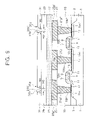
- FIGS. 5 and 6 are a plan view and a cross-sectional view, respectively, of a phase-change memory device according to some embodiments of the present invention, with the cross-sectional view of FIG. 6 corresponding to a section taken along a line I-I′ shown in FIG. 5 .
- the device includes a semiconductor substrate 1 in which source/drain regions 15 s ′, 15 d , 15 s ′′ are formed between isolation regions 3 in the substrate 1 .
- the source/drain regions 15 s ′, 15 d , 15 s ′′ include lightly doped regions 11 and have respective metal silicide layers 17 formed thereon.
- Gate structures 10 a , 10 b are disposed between respective pairs of the source/drain regions 15 s ′, 15 d , 15 s ′′ and include a gate insulation layer 5 , a gate electrode layer 7 , a capping layer 9 and sidewall spacers 13 .
- a first interlayer dielectric layer 19 is disposed on the substrate 1 .
- Conductive plugs 21 p ′, 21 b , 21 p ′′ pass through openings 19 h ′, 19 b , 19 h ′′ in the first interlayer dielectric 19 , contacting the metal silicide layers 17 on respective ones of the source/drain regions 15 s ′, 15 d , 15 s ′′.
- a second interlayer dielectric layer 23 is disposed on the first interlayer dielectric 19 , and conductive pads 25 p ′, 25 p ′′ and a bit line 25 b therein contact respective ones of the conductive plugs 21 p ′, 21 p ′′, 21 b.
- a third dielectric layer 27 is disposed on the second dielectric layer 23 .
- Conductive small contact plugs 37 a ′, 37 b pass through the third dielectric layer 23 and contact respective ones of the conductive pads 25 p ′, 25 p ′′ through openings having sidewall spacers 35 a , 35 b therein.
- Phase-changeable (e.g., chalcogenide) material regions 39 a , 39 b are disposed on respective ones of the small contact plugs 35 a , 35 b
- upper electrodes 41 a , 41 b are disposed on respective ones of the phase-changeable material regions 39 a , 39 b .
- phase-changeable material regions 39 a , 39 b and the upper electrodes 41 a , 41 b are surrounded by another interlayer dielectric layer 43 .
- Conductive contact plugs 45 a , 45 b contact respective ones of the upper electrodes 41 a , 41 b through respective openings 43 a , 43 b in the interlayer dielectric layer 43 .
- Respective plate lines 47 a , 47 b are disposed on respective ones of the contact plugs 45 a , 45 b .
- the gate structures 10 a , 10 b and the source/drain regions 15 s ′, 15 d , 15 s ′′ form respective transistors that can be used to control current flow through the respective phase-changeable material regions 39 a , 39 b , which serve as information storage elements.
- isolation regions 3 are formed in the semiconductor substrate 1 to define an active region.
- Such isolation regions may be, for example, conventionally formed trench and/or field oxide regions.
- Spaced-apart gate structures 10 a , 10 b may be formed on the substrate 1 in a conventional manner, and include a gate insulation (e.g., silicon oxide) layer 5 , a conductive (e.g., polysilicon and/or metal) gate electrode layer 7 , an insulating (e.g., silicon oxide, silicon nitride and/or silicon oxynitride) capping layer 9 and insulating (e.g., silicon oxide, silicon nitride and/or silicon oxynitride) sidewall spacers 13 .
- a gate insulation e.g., silicon oxide
- a conductive (e.g., polysilicon and/or metal) gate electrode layer 7 e.g., silicon oxide, silicon nitride and/or silicon oxynitride) capping layer 9 and insulating (e.g., silicon oxide, silicon nitride and/or silicon oxynitride) sidewall spacers 13 .
- the source/drain regions 15 s ′, 15 p , 15 s ′′ may also be formed in a conventional fashion, e.g., by impurity ion implantations using various parts of the gate structures 10 a , 10 b as masks.
- the metal silicide layers 17 , the interlayer dielectric layer 19 and the contact plugs 21 p ′, 21 b , and 21 p ′′ may also be formed conventionally.
- the dielectric layer 23 may be formed using, for example, conventional deposition techniques, and the contact pads 25 p ′, 25 p ′′ and bit line 25 may be formed using, for example, conventional patterning, deposition, and planarization techniques.
- a dielectric layer 27 and a sacrificial layer 29 are sequentially formed on the dielectric layer 23 .
- the dielectric layer 27 preferably is a material that is more etch-resistant than the sacrificial layer 29 in a subsequent intermediate etching process described in detail below.
- the dielectric layer 27 be a material of sufficient resistance to erosion in a CMP process that is performed after the etching.
- the dielectric layer 27 may be a silicon nitride and/or silicon oxynitride layer
- the sacrificial layer 29 may be a silicon dioxide layer. It will be appreciated, however, that other combinations of materials be used for the dielectric and sacrificial layers 27 , 29 .
- a photoresist layer is formed on the sacrificial layer 29 , and patterned to form a mask 31 with openings 31 h ′, 31 h ′′ therein that expose underlying portions of the sacrificial layer 29 .
- the patterned photoresist layer 31 may be reflowed (e.g., at about 250° C. to about 350° C.) to reduce the width of the openings 31 h ′, 31 h ′′ from a first width W 1 to a second width W 2 by rounding shoulder portions 31 a , 31 b of the pattern 31 .
- the sacrificial layer 29 and the dielectric layer 27 are etched using the photoresist pattern 31 as a mask, exposing top portions of the pads 25 p ′, 25 p ′′ through openings 33 h ′, 33 h ′′.
- Sidewall spacers 35 a , 35 b may be formed on sidewalls 33 w ′, 33 w ′′ of the openings 33 h ′, 33 h ′′ by removing the photoresist pattern 31 , depositing, for example, silicon nitride and/or silicon oxynitride on the sacrificial layer 27 and into the openings 33 h ′, 33 h ′′, and etching to remove portions of the deposited material from the surface of the sacrificial layer 29 and the bottom of the openings 33 h ′, 33 h ′′.
- the previously described reflowing of the photoresist pattern 31 may be omitted if the spacers 35 a , 35 produce sufficiently narrow openings.
- formation of the spacers 35 a , 35 b may be omitted if the reflow of the photoresist provides sufficient narrowing. In some embodiments, both operations may be performed.
- the use of two layers 27 , 29 results in the sidewalls 33 w ′, 33 w ′′ of the holes 33 h ′, 33 h ′′ including sidewalls 27 w , 29 w of the dielectric layer 27 and the sacrificial layer 29 , respectively.
- the openings 33 h ′, 33 h ′′ are generally flared, with a greater amount of flaring being present near the tops of the openings 33 h ′, 33 h ′′ in the sidewalls 29 w of the sacrificial layer 29 .
- the maximum width W 3 of the openings 33 h ′, 33 h ′′ at the sidewalls 27 w of the dielectric layer 27 is generally less than the maximum width at the sidewalls 29 w of the sacrificial layer 29 .
- a conductive material such as titanium nitride, is deposited on the sacrificial layer and into the openings 33 h ′, 33 h ′′, and a first CMP operation is performed to remove portions of the conductive layer and expose the sacrificial layer 29 , thus forming conductive small contact plugs 37 a , 37 b in the openings 33 h ′, 33 h ′′.
- the sacrificial layer 29 is then removed by etching (e.g., dry etching) to expose the dielectric layer 27 .
- etching e.g., dry etching
- a dry etching using an isotropic process is preferable.
- the etching leaves portions of the plugs 37 a , 37 b and the sidewall spacers 35 a , 35 b protruding from the dielectric layer 27 .
- Polymer residue present on the surface of the dielectric layer 27 may be removed by ashing with an oxygen plasma, and cleaning with an HF solution.
- the protruding portions of the plugs 37 a , 37 b and the sidewall spacers 35 a , 35 b may then be removed with a second CMP operation to produce reduced-size small contact plugs 37 a ′, 37 b ′.
- the plugs 37 a ′, 37 b ′ may have a desirable and more uniform narrowness Wh.
- Phase-changeable material regions 39 a , 39 b , upper electrodes 41 a , 41 b and interlayer dielectric layer 43 may be formed on the plugs 37 a ′, 37 b ′ using conventional processes.
- the present invention may provide many advantages.
- small contact plugs may be more precisely and uniformly fabricated.
- the use of a two-CMP process with intermediate etching can improve planarity by reducing effects such as edge over-erosion.
- edge over-erosion can allow subsequent planarization steps to be avoided.
- the use of sacrificial layers and/or a multi-CMP process as described above can allow other structures, such as wiring patterns, contacts or vias, to be more precisely fabricated, and can also maintain planarity for photolithographic alignment and other purposes.
Abstract
A dielectric layer is formed on a region of a microelectronic substrate. A sacrificial layer is formed on the dielectric layer, and portions of the sacrificial layer and the dielectric layer are removed to form an opening that exposes a portion of the region. A conductive layer is formed on the sacrificial layer and in the opening. Portions of the sacrificial layer and the conductive layer on the dielectric layer are removed to leave a conductive plug in the dielectric layer and in contact with the region. Removal of the sacrificial layer and portions of the conductive layer on the dielectric layer may include polishing to expose the sacrificial layer and to leave a conductive plug in the sacrificial layer and the dielectric layer, etching the sacrificial layer to expose the dielectric layer and leave a portion of the conductive plug protruding from the dielectric layer, and polishing to remove the protruding portion of the conductive plug. Phase-change memory devices formed by such techniques are also discussed.
Description
This application is a divisional of U.S. application Ser. No. 10/873,388, filed Jun. 22, 2004, now U.S. Pat. No. 7,291,556 which claims priority to Korean Application Nos. 2003-90874 and 2004-22720, filed on Dec. 12, 2003 and Apr. 1, 2004, respectively, in the Korean Intellectual Property Office, the disclosures of which are incorporated herein in their entirety by reference.
The present invention relates to integrated circuit fabrication techniques, and more particularly, to techniques for fabricating small features, such as contacts, in integrated circuit devices, such as phase-change memory devices.
Factors, such as an ongoing desire for increased circuit integration and the development of new device configurations (e.g., new memory cell types) that are scaleable to extremely small dimensions, have led to an increasing need for techniques for fabricating very small features in integrated circuit devices. Lower bounds on feature size often arise from constraints of photolithography, i.e., the resolution to which layers can be patterned and properly aligned may constrain the size of features that can be fabricated. Techniques, such as the use of sidewall spacers to reduce patterned dimensions of objects like holes in material layers and the use of creative etching techniques, have been developed to lessen some of these constraints, but other barriers to reliably and repeatably forming small structures still remain.
Damascene processes are commonly used in integrated circuit processing to form features such as contacts and wiring patterns. For example, in a typical conventional damascene process, a silicon dioxide layer is formed on a microelectronic substrate. A groove (for wiring) and/or an opening to an underlying region (for a contact) is formed in the dielectric layer. A conductive layer (e.g., a metal containing layer) is then deposited on the dielectric layer, filling the groove and/or opening. Chemical mechanical polishing (CMP) may then be used to remove portions of the conductive layer disposed on the dielectric layer, thus leaving a wiring pattern in the groove and/or a contact plug in the opening.
Such techniques may be used, for example, in fabricating a lower electrode contact (or “small contact”) that provides a high current density path for heating a phase-changeable material (e.g., chalcogenide) region in a phase-change memory device. In a typical fabrication process for such a cell, a dielectric layer is formed over a conductive plug or pad that is electrically coupled to a source/drain region of an access transistor formed on a semiconductor substrate, and a small contact hole is made in the dielectric layer to expose an upper surface of the plug or pad. A metal-containing material is then deposited on the dielectric layer and in the small contact hole. Excess material disposed on the dielectric layer is then removed using CMP to leave a small contact plug in the contact hole. A phase-changeable material region is then formed on the surface of the dielectric layer and the small contact plug, and an upper electrode is formed on the phase-changeable material region. Examples of techniques for forming contacts for phase-change memory devices are described in U.S. Pat. No. 6,117,720 and U.S. Pat. No. 6,147,395.
Conventional processes may have characteristics that can limit the ability to reliably and repeatably make small contacts or other small structures. In particular, in many applications, it may be desirable to remove a metal or other conductive layer as close as possible to the top of a surrounding dielectric layer or region. For example, in forming small contact plugs for phase-change memory cells along the lines described above, it is generally desirable to remove the metal layer down to a shoulder of the opening in the dielectric layer so that the surface area of the individual contact plugs is made as small as possible while maintaining the planarity of the substrate surface and uniformity among the contact plugs. However, using a conventional process as described above can result in less than desirable results due to flaring at the mouths of the contact holes and/or dishing, overerosion, edge over-erosion, and other surface non-uniformity arising from the CMP. Such effects may be exacerbated by variation in pattern density across the surface of the wafer.
According to some embodiments of the present invention, a contact for a region of a microelectronic substrate is formed. A dielectric layer is formed on the region. A sacrificial layer is formed on the dielectric layer. Portions of the sacrificial layer and the dielectric layer are removed to form an opening that exposes a portion of the region. A conductive layer is formed on the sacrificial layer and in the opening. The substrate is polished to expose the sacrificial layer and to leave a conductive plug in the sacrificial layer and the dielectric layer. The sacrificial layer is etched to expose the dielectric layer and leave a portion of the conductive plug protruding from the dielectric layer. The substrate is again polished to remove the protruding portion of the conductive plug and thereby form the contact. In some embodiments, the sacrificial layer includes silicon dioxide, the dielectric layer includes silicon nitride and/or silicon oxynitride, and the conductive layer includes a metal-containing layer, such as a tungsten layer. A polymer residue on the substrate may be ashed after the first polishing step and/or the second polishing step, and the ashed polymer residue may be removed with a cleaning solution, e.g., hydrofluoric acid.
In further embodiments, a photoresist layer is formed on the sacrificial layer and patterned to form an opening that exposes a portion of the sacrificial layer. The patterned photoresist layer is reflowed to narrow the opening. The sacrificial layer and the dielectric layer are etched using the reflowed photoresist layer as an etching mask to form an opening that exposes a portion of the region. This may be followed by forming a sidewall spacer that narrows the opening, and forming a conductive layer that fills the narrowed opening. The reflow step or the formation of the sidewall spacer may be omitted in some embodiments.
According to additional embodiments of the present invention, a dielectric layer is formed on a region of a microelectronic substrate. A sacrificial layer is formed on the dielectric layer, and portions of the sacrificial layer and the dielectric layer are removed to form an opening that exposes a portion of the region. A conductive layer is formed on the sacrificial layer and in the opening. Portions of the sacrificial layer and the conductive layer on the dielectric layer are removed to leave a conductive plug in the dielectric layer and in contact with the region. Removal of the sacrificial layer and portions of the conductive layer on the dielectric layer may include polishing to expose the sacrificial layer and to leave a conductive plug in the sacrificial layer and the dielectric layer, etching the sacrificial layer to expose the dielectric layer and leave a portion of the conductive plug protruding from the dielectric layer, and polishing to remove the protruding portion of the conductive plug.
In further embodiments of the present invention, a method of fabricating a microelectronic structure includes forming a dielectric layer on a substrate and forming a sacrificial layer having an etching selectivity with respect to the dielectric layer on the dielectric layer. An opening is formed that extends through the sacrificial layer and at least partially into the dielectric layer. A conductive material, e.g., a metal or metal-containing material, is deposited on the sacrificial layer and into the opening. The substrate is polished to expose the sacrificial layer and leave a conductive region in the sacrificial layer and the dielectric layer. The sacrificial layer is etched to expose the dielectric layer and leave a portion of the conductive region protruding therefrom. The substrate is again polished to remove the protruding portion of the conductive region.
According to some embodiments of the present invention, a phase-change memory element is fabricated. A first conductive region is formed on a microelectronic substrate. A dielectric layer is formed on the first conductive region, and a sacrificial layer is formed on the dielectric layer. Portions of the sacrificial layer and the dielectric layer are removed to form an opening that exposes a portion of the first conductive region, and a conductive layer is formed on the sacrificial layer that extends through the opening to contact the first conductive region. The sacrificial layer and portions of the conductive layer are removed to leave a conductive plug in the dielectric layer and in contact with the first conductive region. A phase changeable material region is formed on the conductive plug, and a second conductive region is formed on the phase changeable material region. Removal of the sacrificial layer and portions of the conductive layer may include polishing to expose the sacrificial layer and leave a conductive plug in the sacrificial layer and the dielectric layer, etching the sacrificial layer to expose the dielectric layer and leave a portion of the conductive plug protruding from the dielectric layer, and polishing to remove the protruding portion of the plug. The sacrificial layer may include silicon dioxide, the dielectric layer may include silicon nitride and/or silicon oxynitride, and the conductive layer may include a metal-containing layer.
In some embodiments, a photoresist layer is formed on the sacrificial layer and patterned to form an opening that exposes a portion of the sacrificial layer. The photoresist layer is reflowed to narrow the opening, and the sacrificial layer and the dielectric layer are etched using the reflowed photoresist layer as an etching mask to form an opening that exposes a portion of the first conductive region. A sidewall spacer that narrows the opening may be formed, and the conductive layer may include a conductive layer that fills the narrowed opening.
According to further embodiments of the present invention, a phase-change memory device includes a microelectronic substrate including a first conductive region, a silicon nitride layer and/or a silicon oxynitride layer on the first conductive region, a contact plug extending from a surface of the silicon nitride layer and/or a silicon oxynitride layer through an opening therein to the first conductive region, a phase changeable material region on the contact plug and the silicon nitride layer and/or a silicon oxynitride layer, and a second conductive region on the phase changeable material region. The device may further include a sidewall spacer in the opening in the silicon nitride layer and/or a silicon oxynitride layer.
The present invention now will be described more fully hereinafter with reference to the accompanying drawings, in which typical and exemplary embodiments of the invention are shown. This invention may, however, be embodied in many different forms and should not be construed as limited to the embodiments set forth herein. Rather, these embodiments are provided so that this disclosure will be thorough and complete, and will fully convey the scope of the invention to those skilled in the art.
In the drawings, the thickness of layers and regions are exaggerated for clarity. It will be understood that when an element such as a layer, region or substrate is referred to as being “on” another element, it can be directly on the other element or intervening elements may also be present. Furthermore, relative terms, such as “beneath,” may be used herein to describe one element's relationship to another elements as illustrated in the drawings. It will be understood that relative terms are intended to encompass different orientations of the device in addition to the orientation depicted in the drawings. For example, if the device in the drawings is turned over, elements described as “below” other elements would then be oriented “above” the other elements. The exemplary term “below,” therefore, encompasses both an orientation of above and below.
It will be understood that although the terms “first” and “second” are used herein to describe various regions, layers and/or sections, these regions, layers and/or sections should not be limited by these terms. These terms are only used to distinguish one region, layer or section from another region, layer or section. Thus, a first region, layer or section discussed below could be termed a second region, layer or section, and similarly, a second without departing from the teachings of the present invention. As used herein the term “and/or” includes any and all combinations of one or more of the associated listed items. Like numbers refer to like elements throughout.
As further shown in FIG. 1 , a conductive layer 300 is formed on the sacrificial layer 100, filling the openings 110. In general, the conductive layer 300 may include any of a number of different materials, including, but not limited to, metals, such as aluminum, titanium, copper, and tungsten, and/or metal-containing materials, such as metal suicides or metal nitrides, and/or non-metallic conductors, such as polysilicon. The conductive layer 300 may comprise a single layer or compound layers including, for example, ohmic transition layers, glue layers, contamination barrier layers, spacers, and the like.
Referring to FIG. 2 , a first CMP is performed to remove portions of the metal-containing layer 300 on the sacrificial layer 200 and leave conductive regions 310 in the sacrificial layer 200 and the dielectric layer 100. As shown, the CMP may erode portions of the sacrificial layer 200, and the conductive regions 310 may be significantly non-uniform in extent.
Referring to FIG. 3 , the sacrificial layer 200 is etched (e.g., dry or wet etched) away to expose the dielectric layer 100, leaving portions 310 a of the conductive regions 310 protruding from the dielectric layer. An ashing process using an oxygen plasma and subsequent cleaning using, for example, a dilute HF solution, may be performed after this etching to remove polymer residues that may remain on the dielectric layer 100. Such residues may have their source in particles left on the substrate by polymer polishing pads used in the preceding CMP.
Referring to FIG. 4 , a second CMP is performed to remove the protruding portions 310 a of the conductive regions 310, leaving reduced-size conductive regions 310′ in the dielectric layer 100. As shown, some erosion of the dielectric layer 100 and non-uniformity in the conductive regions 310′ may occur as a result of this second CMP. However, it is believed that, because the second CMP process can be highly selective of the exposed protruding portions 310 a of the conductive regions 310, the degree of erosion of dielectric layer 100 can be limited to an acceptable level. Accordingly, the size of the conductive regions 310′ may be more uniform using the above-described process, which includes two CMP processes and an intervening etching process, in comparison to a conventional single-CMP approach. To prepare the resulting structure for further fabrication operations, for example, formation of one or more chalcogenide regions on the conductive regions 310′ as would be done in fabricating a phase-change memory device, polymer residues may be removed by an oxygen plasma ashing process and a subsequent cleaning using, for example, an HF solution.
A first interlayer dielectric layer 19 is disposed on the substrate 1. Conductive plugs 21 p′, 21 b, 21 p″ pass through openings 19 h′, 19 b, 19 h″ in the first interlayer dielectric 19, contacting the metal silicide layers 17 on respective ones of the source/drain regions 15 s′, 15 d, 15 s″. A second interlayer dielectric layer 23 is disposed on the first interlayer dielectric 19, and conductive pads 25 p′, 25 p″ and a bit line 25 b therein contact respective ones of the conductive plugs 21 p′, 21 p″, 21 b.
A third dielectric layer 27 is disposed on the second dielectric layer 23. Conductive small contact plugs 37 a′, 37 b pass through the third dielectric layer 23 and contact respective ones of the conductive pads 25 p′, 25 p″ through openings having sidewall spacers 35 a, 35 b therein. Phase-changeable (e.g., chalcogenide) material regions 39 a, 39 b are disposed on respective ones of the small contact plugs 35 a, 35 b, and upper electrodes 41 a, 41 b are disposed on respective ones of the phase- changeable material regions 39 a, 39 b. The phase- changeable material regions 39 a, 39 b and the upper electrodes 41 a, 41 b are surrounded by another interlayer dielectric layer 43. Conductive contact plugs 45 a, 45 b contact respective ones of the upper electrodes 41 a, 41 b through respective openings 43 a, 43 b in the interlayer dielectric layer 43. Respective plate lines 47 a, 47 b are disposed on respective ones of the contact plugs 45 a, 45 b. It will be appreciated that the gate structures 10 a, 10 b and the source/drain regions 15 s′, 15 d, 15 s″ form respective transistors that can be used to control current flow through the respective phase- changeable material regions 39 a, 39 b, which serve as information storage elements.
Exemplary operations for fabricating the device illustrated in FIGS. 5 and 6 will now be explained with reference to FIGS. 7-12 . Referring to FIG. 7 , isolation regions 3 are formed in the semiconductor substrate 1 to define an active region. Such isolation regions may be, for example, conventionally formed trench and/or field oxide regions. Spaced-apart gate structures 10 a, 10 b may be formed on the substrate 1 in a conventional manner, and include a gate insulation (e.g., silicon oxide) layer 5, a conductive (e.g., polysilicon and/or metal) gate electrode layer 7, an insulating (e.g., silicon oxide, silicon nitride and/or silicon oxynitride) capping layer 9 and insulating (e.g., silicon oxide, silicon nitride and/or silicon oxynitride) sidewall spacers 13. The source/drain regions 15 s′, 15 p, 15 s″ (including the lightly doped regions 11) may also be formed in a conventional fashion, e.g., by impurity ion implantations using various parts of the gate structures 10 a, 10 b as masks. The metal silicide layers 17, the interlayer dielectric layer 19 and the contact plugs 21 p′, 21 b, and 21 p″ may also be formed conventionally. Referring to FIG. 8 , the dielectric layer 23 may be formed using, for example, conventional deposition techniques, and the contact pads 25 p′, 25 p″ and bit line 25 may be formed using, for example, conventional patterning, deposition, and planarization techniques.
A dielectric layer 27 and a sacrificial layer 29 are sequentially formed on the dielectric layer 23. The dielectric layer 27 preferably is a material that is more etch-resistant than the sacrificial layer 29 in a subsequent intermediate etching process described in detail below. Also, it is preferable that the dielectric layer 27 be a material of sufficient resistance to erosion in a CMP process that is performed after the etching. For example, the dielectric layer 27 may be a silicon nitride and/or silicon oxynitride layer, and the sacrificial layer 29 may be a silicon dioxide layer. It will be appreciated, however, that other combinations of materials be used for the dielectric and sacrificial layers 27, 29.
Referring to FIG. 9 , a photoresist layer is formed on the sacrificial layer 29, and patterned to form a mask 31 with openings 31 h′, 31 h″ therein that expose underlying portions of the sacrificial layer 29. As shown in FIG. 9 , the patterned photoresist layer 31 may be reflowed (e.g., at about 250° C. to about 350° C.) to reduce the width of the openings 31 h′, 31 h″ from a first width W1 to a second width W2 by rounding shoulder portions 31 a, 31 b of the pattern 31.
As illustrated by FIG. 10 , the sacrificial layer 29 and the dielectric layer 27 are etched using the photoresist pattern 31 as a mask, exposing top portions of the pads 25 p′, 25 p″ through openings 33 h′, 33 h″. Sidewall spacers 35 a, 35 b may be formed on sidewalls 33 w′, 33 w″ of the openings 33 h′, 33 h″ by removing the photoresist pattern 31, depositing, for example, silicon nitride and/or silicon oxynitride on the sacrificial layer 27 and into the openings 33 h′, 33 h″, and etching to remove portions of the deposited material from the surface of the sacrificial layer 29 and the bottom of the openings 33 h′, 33 h″. As the spacers 35 a, 35 b serve to further narrow the openings 33 h′, 33 h″, the previously described reflowing of the photoresist pattern 31 may be omitted if the spacers 35 a, 35 produce sufficiently narrow openings. Similarly, formation of the spacers 35 a, 35 b may be omitted if the reflow of the photoresist provides sufficient narrowing. In some embodiments, both operations may be performed.
As also shown in FIG. 10 , the use of two layers 27, 29 results in the sidewalls 33 w′, 33 w″ of the holes 33 h′, 33 h″ including sidewalls 27 w, 29 w of the dielectric layer 27 and the sacrificial layer 29, respectively. The openings 33 h′, 33 h″ are generally flared, with a greater amount of flaring being present near the tops of the openings 33 h′, 33 h″ in the sidewalls 29 w of the sacrificial layer 29. The maximum width W3 of the openings 33 h′, 33 h″ at the sidewalls 27 w of the dielectric layer 27 is generally less than the maximum width at the sidewalls 29 w of the sacrificial layer 29.
Referring to FIG. 11 , a conductive material, such as titanium nitride, is deposited on the sacrificial layer and into the openings 33 h′, 33 h″, and a first CMP operation is performed to remove portions of the conductive layer and expose the sacrificial layer 29, thus forming conductive small contact plugs 37 a, 37 b in the openings 33 h′, 33 h″. The sacrificial layer 29 is then removed by etching (e.g., dry etching) to expose the dielectric layer 27. For the illustrated embodiments, a dry etching using an isotropic process is preferable. The etching leaves portions of the plugs 37 a, 37 b and the sidewall spacers 35 a, 35 b protruding from the dielectric layer 27. Polymer residue present on the surface of the dielectric layer 27 may be removed by ashing with an oxygen plasma, and cleaning with an HF solution.
Referring to FIG. 12 , the protruding portions of the plugs 37 a, 37 b and the sidewall spacers 35 a, 35 b may then be removed with a second CMP operation to produce reduced-size small contact plugs 37 a′, 37 b′. Through the use of the sacrificial layer 29 to reduce the flaring of the contact hole and a contact formation process that involves two CMP steps with an intermediate etching, the plugs 37 a′, 37 b′ may have a desirable and more uniform narrowness Wh. Phase- changeable material regions 39 a, 39 b, upper electrodes 41 a, 41 b and interlayer dielectric layer 43 may be formed on the plugs 37 a′, 37 b′ using conventional processes.
The present invention may provide many advantages. In the illustrated phase-change memory fabrication described above, small contact plugs may be more precisely and uniformly fabricated. In addition, the use of a two-CMP process with intermediate etching can improve planarity by reducing effects such as edge over-erosion. Thus, for example, even though an addition CMP process is performed, reduction in edge over-erosion can allow subsequent planarization steps to be avoided. In other applications, the use of sacrificial layers and/or a multi-CMP process as described above can allow other structures, such as wiring patterns, contacts or vias, to be more precisely fabricated, and can also maintain planarity for photolithographic alignment and other purposes.
In the drawings and specification, there have been disclosed typical embodiments of the invention and, although specific terms are employed, they are used in a generic and descriptive sense only and not for purposes of limitation, the scope of the invention being set forth in the following claims.
Claims (12)
1. A phase-change memory device, comprising:
a microelectronic substrate including a first conductive region;
a silicon nitride layer and/or a silicon oxynitride layer on the first conductive region;
a contact plug extending from a surface of the silicon nitride layer and/or a silicon oxynitride layer through an opening therein to the first conductive region;
a phase changeable material region on the contact plug and the silicon nitride layer and/or a silicon oxynitride layer; and
a second conductive region on the phase changeable material region.
2. A device according to claim 1 , further comprising a sidewall spacer in the opening in the silicon nitride layer and/or a silicon oxynitride layer.
3. A device according to claim 2 , wherein the sidewall spacer comprises silicon nitride.
4. A device according to claim 1 , wherein the contact plug comprises tungsten.
5. A semiconductor memory device, comprising:
a microelectronic substrate including a first conductive region;
a silicon nitride layer and/or a silicon oxynitride layer on the first conductive region;
a contact plug extending from a surface of the silicon nitride layer and/or a silicon oxynitride layer through an opening therein to the first conductive region;
a phase changeable material region on the contact plug and the silicon nitride layer and/or a silicon oxynitride layer; and
a second conductive region on the phase changeable material region.
6. A device according to claim 5 , further comprising a sidewall spacer in the opening in the silicon nitride layer and/or a silicon oxynitride layer.
7. A device according to claim 6 , wherein the sidewall spacer comprises silicon nitride.
8. A device according to claim 5 , wherein the contact plug comprises a metal-containing material.
9. A semiconductor memory device including a phase changeable material, comprising:
a semiconductor substrate;
an interlayer dielectric layer formed on the substrate;
a first conductive region formed in the interlayer dielectric layer;
a silicon nitride layer and/or a silicon oxynitride layer on the first conductive region and the interlayer dielectric layer;
a contact plug extending from a surface of the silicon nitride layer and/or silicon oxynitride layer through an opening therein to a portion of the first conductive region;
a phase changeable material region on the contact plug and the silicon nitride layer and/or silicon oxynitride layer; and
a second conductive region on the phase changeable material region.
10. A device according to claim 9 , further comprising a sidewall spacer in the opening in the silicon nitride layer and/or silicon oxynitride layer.
11. A device according to claim 10 , wherein the sidewall spacer comprises silicon nitride.
12. A device according to claim 9 , wherein the contact plug comprises a metal containing material.
Priority Applications (1)
| Application Number | Priority Date | Filing Date | Title |
|---|---|---|---|
| US11/860,674 US7612359B2 (en) | 2003-12-12 | 2007-09-25 | Microelectronic devices using sacrificial layers and structures fabricated by same |
Applications Claiming Priority (6)
| Application Number | Priority Date | Filing Date | Title |
|---|---|---|---|
| KR20030090874 | 2003-12-12 | ||
| KR2003-90874 | 2003-12-12 | ||
| KR20040022720 | 2004-04-01 | ||
| KR2004-22720 | 2004-04-01 | ||
| US10/873,388 US7291556B2 (en) | 2003-12-12 | 2004-06-22 | Method for forming small features in microelectronic devices using sacrificial layers |
| US11/860,674 US7612359B2 (en) | 2003-12-12 | 2007-09-25 | Microelectronic devices using sacrificial layers and structures fabricated by same |
Related Parent Applications (1)
| Application Number | Title | Priority Date | Filing Date |
|---|---|---|---|
| US10/873,388 Division US7291556B2 (en) | 2003-12-12 | 2004-06-22 | Method for forming small features in microelectronic devices using sacrificial layers |
Publications (2)
| Publication Number | Publication Date |
|---|---|
| US20080011999A1 US20080011999A1 (en) | 2008-01-17 |
| US7612359B2 true US7612359B2 (en) | 2009-11-03 |
Family
ID=34656340
Family Applications (2)
| Application Number | Title | Priority Date | Filing Date |
|---|---|---|---|
| US10/873,388 Expired - Fee Related US7291556B2 (en) | 2003-12-12 | 2004-06-22 | Method for forming small features in microelectronic devices using sacrificial layers |
| US11/860,674 Expired - Fee Related US7612359B2 (en) | 2003-12-12 | 2007-09-25 | Microelectronic devices using sacrificial layers and structures fabricated by same |
Family Applications Before (1)
| Application Number | Title | Priority Date | Filing Date |
|---|---|---|---|
| US10/873,388 Expired - Fee Related US7291556B2 (en) | 2003-12-12 | 2004-06-22 | Method for forming small features in microelectronic devices using sacrificial layers |
Country Status (2)
| Country | Link |
|---|---|
| US (2) | US7291556B2 (en) |
| KR (1) | KR100615090B1 (en) |
Families Citing this family (125)
| Publication number | Priority date | Publication date | Assignee | Title |
|---|---|---|---|---|
| KR100668825B1 (en) * | 2004-06-30 | 2007-01-16 | 주식회사 하이닉스반도체 | Phase-change memory device and method for manufacturing the same |
| KR100639206B1 (en) * | 2004-06-30 | 2006-10-30 | 주식회사 하이닉스반도체 | Phase-change memory device and method for manufacturing the same |
| KR100615598B1 (en) * | 2004-07-19 | 2006-08-25 | 삼성전자주식회사 | Semiconductor Devices Having A Planarization Isolating Layer And Methods Of Forming The Same |
| KR100568543B1 (en) * | 2004-08-31 | 2006-04-07 | 삼성전자주식회사 | Method of forming a phase change memory device having a small area of contact |
| KR100626388B1 (en) * | 2004-10-19 | 2006-09-20 | 삼성전자주식회사 | Phase-changable memory device and method of forming the same |
| KR100620064B1 (en) * | 2004-12-28 | 2006-09-08 | 주식회사 하이닉스반도체 | Method for forming storagenode contact in semiconductor device |
| KR100632656B1 (en) * | 2005-05-23 | 2006-10-11 | 주식회사 하이닉스반도체 | Method of forming a bit line in flash memory device |
| KR100650735B1 (en) * | 2005-05-26 | 2006-11-27 | 주식회사 하이닉스반도체 | Phase change ram device and method of manufacturing the same |
| KR100668846B1 (en) * | 2005-06-10 | 2007-01-16 | 주식회사 하이닉스반도체 | Method of manufacturing phase change RAM device |
| KR100689831B1 (en) * | 2005-06-20 | 2007-03-08 | 삼성전자주식회사 | Phase change memory cells having a cell diode and a bottom electrode self-aligned with each other and methods of fabricating the same |
| US7651906B2 (en) * | 2005-06-20 | 2010-01-26 | Samsung Electronics Co., Ltd. | Integrated circuit devices having a stress buffer spacer and methods of fabricating the same |
| KR100681266B1 (en) * | 2005-07-25 | 2007-02-09 | 삼성전자주식회사 | Method of manufacturing a variable resistance and method of manufacturing a phase changeable memory device using the same |
| JP2007036126A (en) * | 2005-07-29 | 2007-02-08 | Fujitsu Ltd | Semiconductor device and method for manufacturing the same |
| KR100706798B1 (en) * | 2005-09-28 | 2007-04-12 | 삼성전자주식회사 | Method of cleaning substrate having exposed surfaces of silicon and silicon germanium and method of forming semiconductor device using the same |
| US7635855B2 (en) | 2005-11-15 | 2009-12-22 | Macronix International Co., Ltd. | I-shaped phase change memory cell |
| US7786460B2 (en) | 2005-11-15 | 2010-08-31 | Macronix International Co., Ltd. | Phase change memory device and manufacturing method |
| US7414258B2 (en) | 2005-11-16 | 2008-08-19 | Macronix International Co., Ltd. | Spacer electrode small pin phase change memory RAM and manufacturing method |
| US7829876B2 (en) | 2005-11-21 | 2010-11-09 | Macronix International Co., Ltd. | Vacuum cell thermal isolation for a phase change memory device |
| US7449710B2 (en) | 2005-11-21 | 2008-11-11 | Macronix International Co., Ltd. | Vacuum jacket for phase change memory element |
| US7599217B2 (en) * | 2005-11-22 | 2009-10-06 | Macronix International Co., Ltd. | Memory cell device and manufacturing method |
| US7688619B2 (en) | 2005-11-28 | 2010-03-30 | Macronix International Co., Ltd. | Phase change memory cell and manufacturing method |
| US7459717B2 (en) | 2005-11-28 | 2008-12-02 | Macronix International Co., Ltd. | Phase change memory cell and manufacturing method |
| US7521364B2 (en) * | 2005-12-02 | 2009-04-21 | Macronix Internation Co., Ltd. | Surface topology improvement method for plug surface areas |
| KR100721624B1 (en) * | 2005-12-21 | 2007-05-23 | 매그나칩 반도체 유한회사 | Manufacturing method for shallow trench isolation semiconductor device |
| US7531825B2 (en) | 2005-12-27 | 2009-05-12 | Macronix International Co., Ltd. | Method for forming self-aligned thermal isolation cell for a variable resistance memory array |
| US8062833B2 (en) | 2005-12-30 | 2011-11-22 | Macronix International Co., Ltd. | Chalcogenide layer etching method |
| US7741636B2 (en) | 2006-01-09 | 2010-06-22 | Macronix International Co., Ltd. | Programmable resistive RAM and manufacturing method |
| US7560337B2 (en) | 2006-01-09 | 2009-07-14 | Macronix International Co., Ltd. | Programmable resistive RAM and manufacturing method |
| US7595218B2 (en) * | 2006-01-09 | 2009-09-29 | Macronix International Co., Ltd. | Programmable resistive RAM and manufacturing method |
| US7629265B2 (en) * | 2006-02-13 | 2009-12-08 | Macronix International Co., Ltd. | Cleaning method for use in semiconductor device fabrication |
| KR100822800B1 (en) * | 2006-05-24 | 2008-04-17 | 삼성전자주식회사 | Phase Change Material Memory Device and Mehtod For Forming The Same |
| TWI310558B (en) * | 2006-06-02 | 2009-06-01 | Ind Tech Res Inst | Phase change memory cell |
| US7696506B2 (en) * | 2006-06-27 | 2010-04-13 | Macronix International Co., Ltd. | Memory cell with memory material insulation and manufacturing method |
| US7785920B2 (en) | 2006-07-12 | 2010-08-31 | Macronix International Co., Ltd. | Method for making a pillar-type phase change memory element |
| KR100734325B1 (en) * | 2006-07-14 | 2007-07-02 | 삼성전자주식회사 | Method of fabricating a semiconductor device |
| KR100749740B1 (en) * | 2006-08-01 | 2007-08-17 | 삼성전자주식회사 | Phase-change memory device and method of manufacturing the same |
| US7772581B2 (en) | 2006-09-11 | 2010-08-10 | Macronix International Co., Ltd. | Memory device having wide area phase change element and small electrode contact area |
| US7504653B2 (en) | 2006-10-04 | 2009-03-17 | Macronix International Co., Ltd. | Memory cell device with circumferentially-extending memory element |
| US7863655B2 (en) | 2006-10-24 | 2011-01-04 | Macronix International Co., Ltd. | Phase change memory cells with dual access devices |
| US7476587B2 (en) | 2006-12-06 | 2009-01-13 | Macronix International Co., Ltd. | Method for making a self-converged memory material element for memory cell |
| US7903447B2 (en) | 2006-12-13 | 2011-03-08 | Macronix International Co., Ltd. | Method, apparatus and computer program product for read before programming process on programmable resistive memory cell |
| KR100791077B1 (en) * | 2006-12-13 | 2008-01-03 | 삼성전자주식회사 | Phase change memory device with small transition volume and method of forming the same |
| US8188569B2 (en) * | 2006-12-15 | 2012-05-29 | Qimonda Ag | Phase change random access memory device with transistor, and method for fabricating a memory device |
| US7718989B2 (en) | 2006-12-28 | 2010-05-18 | Macronix International Co., Ltd. | Resistor random access memory cell device |
| KR100809341B1 (en) | 2007-02-01 | 2008-03-05 | 삼성전자주식회사 | Nonvolatile memory device using variable resistive element and fabricating method thereof |
| US7619311B2 (en) | 2007-02-02 | 2009-11-17 | Macronix International Co., Ltd. | Memory cell device with coplanar electrode surface and method |
| US7884343B2 (en) * | 2007-02-14 | 2011-02-08 | Macronix International Co., Ltd. | Phase change memory cell with filled sidewall memory element and method for fabricating the same |
| US7956344B2 (en) | 2007-02-27 | 2011-06-07 | Macronix International Co., Ltd. | Memory cell with memory element contacting ring-shaped upper end of bottom electrode |
| TW200840022A (en) * | 2007-03-27 | 2008-10-01 | Ind Tech Res Inst | Phase-change memory devices and methods for fabricating the same |
| US7786461B2 (en) | 2007-04-03 | 2010-08-31 | Macronix International Co., Ltd. | Memory structure with reduced-size memory element between memory material portions |
| TWI402980B (en) | 2007-07-20 | 2013-07-21 | Macronix Int Co Ltd | Resistive memory structure with buffer layer |
| US7729161B2 (en) | 2007-08-02 | 2010-06-01 | Macronix International Co., Ltd. | Phase change memory with dual word lines and source lines and method of operating same |
| KR100892667B1 (en) | 2007-08-14 | 2009-04-15 | 주식회사 하이닉스반도체 | Phase-change memory device and fabrication method thereof |
| US8178386B2 (en) | 2007-09-14 | 2012-05-15 | Macronix International Co., Ltd. | Phase change memory cell array with self-converged bottom electrode and method for manufacturing |
| US7642125B2 (en) | 2007-09-14 | 2010-01-05 | Macronix International Co., Ltd. | Phase change memory cell in via array with self-aligned, self-converged bottom electrode and method for manufacturing |
| US7919766B2 (en) | 2007-10-22 | 2011-04-05 | Macronix International Co., Ltd. | Method for making self aligning pillar memory cell device |
| KR101099958B1 (en) * | 2007-11-20 | 2011-12-28 | 주식회사 하이닉스반도체 | Method of forming metal line of semiconductor devices |
| KR101386434B1 (en) * | 2007-11-27 | 2014-04-25 | 삼성전자주식회사 | Semiconductor Device And Method Of Fabricating The Same |
| US7646631B2 (en) * | 2007-12-07 | 2010-01-12 | Macronix International Co., Ltd. | Phase change memory cell having interface structures with essentially equal thermal impedances and manufacturing methods |
| KR20090061509A (en) * | 2007-12-11 | 2009-06-16 | 주식회사 동부하이텍 | Multi-bit memory cell structure and method thereof |
| US7879643B2 (en) | 2008-01-18 | 2011-02-01 | Macronix International Co., Ltd. | Memory cell with memory element contacting an inverted T-shaped bottom electrode |
| KR100953016B1 (en) | 2008-01-22 | 2010-04-14 | 주식회사 하이닉스반도체 | Method of manufacturing a semiconductor device |
| US7879645B2 (en) | 2008-01-28 | 2011-02-01 | Macronix International Co., Ltd. | Fill-in etching free pore device |
| US8158965B2 (en) | 2008-02-05 | 2012-04-17 | Macronix International Co., Ltd. | Heating center PCRAM structure and methods for making |
| KR100968426B1 (en) * | 2008-02-28 | 2010-07-07 | 주식회사 하이닉스반도체 | Vertical channel transistor in semiconductor device and method for forming the same |
| US8084842B2 (en) | 2008-03-25 | 2011-12-27 | Macronix International Co., Ltd. | Thermally stabilized electrode structure |
| US8030634B2 (en) | 2008-03-31 | 2011-10-04 | Macronix International Co., Ltd. | Memory array with diode driver and method for fabricating the same |
| US7825398B2 (en) | 2008-04-07 | 2010-11-02 | Macronix International Co., Ltd. | Memory cell having improved mechanical stability |
| US7791057B2 (en) | 2008-04-22 | 2010-09-07 | Macronix International Co., Ltd. | Memory cell having a buried phase change region and method for fabricating the same |
| US8077505B2 (en) | 2008-05-07 | 2011-12-13 | Macronix International Co., Ltd. | Bipolar switching of phase change device |
| US7701750B2 (en) | 2008-05-08 | 2010-04-20 | Macronix International Co., Ltd. | Phase change device having two or more substantial amorphous regions in high resistance state |
| US8415651B2 (en) | 2008-06-12 | 2013-04-09 | Macronix International Co., Ltd. | Phase change memory cell having top and bottom sidewall contacts |
| US8134857B2 (en) | 2008-06-27 | 2012-03-13 | Macronix International Co., Ltd. | Methods for high speed reading operation of phase change memory and device employing same |
| KR101487370B1 (en) * | 2008-07-07 | 2015-01-30 | 삼성전자주식회사 | Method of forming a mask layout and mask layout |
| US7932506B2 (en) | 2008-07-22 | 2011-04-26 | Macronix International Co., Ltd. | Fully self-aligned pore-type memory cell having diode access device |
| US7903457B2 (en) | 2008-08-19 | 2011-03-08 | Macronix International Co., Ltd. | Multiple phase change materials in an integrated circuit for system on a chip application |
| US7719913B2 (en) | 2008-09-12 | 2010-05-18 | Macronix International Co., Ltd. | Sensing circuit for PCRAM applications |
| US8324605B2 (en) | 2008-10-02 | 2012-12-04 | Macronix International Co., Ltd. | Dielectric mesh isolated phase change structure for phase change memory |
| US7897954B2 (en) | 2008-10-10 | 2011-03-01 | Macronix International Co., Ltd. | Dielectric-sandwiched pillar memory device |
| US8036014B2 (en) * | 2008-11-06 | 2011-10-11 | Macronix International Co., Ltd. | Phase change memory program method without over-reset |
| US8907316B2 (en) | 2008-11-07 | 2014-12-09 | Macronix International Co., Ltd. | Memory cell access device having a pn-junction with polycrystalline and single crystal semiconductor regions |
| US8664689B2 (en) | 2008-11-07 | 2014-03-04 | Macronix International Co., Ltd. | Memory cell access device having a pn-junction with polycrystalline plug and single-crystal semiconductor regions |
| US7869270B2 (en) | 2008-12-29 | 2011-01-11 | Macronix International Co., Ltd. | Set algorithm for phase change memory cell |
| US8089137B2 (en) | 2009-01-07 | 2012-01-03 | Macronix International Co., Ltd. | Integrated circuit memory with single crystal silicon on silicide driver and manufacturing method |
| US8107283B2 (en) | 2009-01-12 | 2012-01-31 | Macronix International Co., Ltd. | Method for setting PCRAM devices |
| US8030635B2 (en) | 2009-01-13 | 2011-10-04 | Macronix International Co., Ltd. | Polysilicon plug bipolar transistor for phase change memory |
| US8064247B2 (en) | 2009-01-14 | 2011-11-22 | Macronix International Co., Ltd. | Rewritable memory device based on segregation/re-absorption |
| US8933536B2 (en) | 2009-01-22 | 2015-01-13 | Macronix International Co., Ltd. | Polysilicon pillar bipolar transistor with self-aligned memory element |
| US8084760B2 (en) | 2009-04-20 | 2011-12-27 | Macronix International Co., Ltd. | Ring-shaped electrode and manufacturing method for same |
| US8173987B2 (en) | 2009-04-27 | 2012-05-08 | Macronix International Co., Ltd. | Integrated circuit 3D phase change memory array and manufacturing method |
| US8097871B2 (en) | 2009-04-30 | 2012-01-17 | Macronix International Co., Ltd. | Low operational current phase change memory structures |
| US7933139B2 (en) | 2009-05-15 | 2011-04-26 | Macronix International Co., Ltd. | One-transistor, one-resistor, one-capacitor phase change memory |
| US8350316B2 (en) | 2009-05-22 | 2013-01-08 | Macronix International Co., Ltd. | Phase change memory cells having vertical channel access transistor and memory plane |
| US7968876B2 (en) | 2009-05-22 | 2011-06-28 | Macronix International Co., Ltd. | Phase change memory cell having vertical channel access transistor |
| US8809829B2 (en) | 2009-06-15 | 2014-08-19 | Macronix International Co., Ltd. | Phase change memory having stabilized microstructure and manufacturing method |
| US8406033B2 (en) | 2009-06-22 | 2013-03-26 | Macronix International Co., Ltd. | Memory device and method for sensing and fixing margin cells |
| US8238149B2 (en) | 2009-06-25 | 2012-08-07 | Macronix International Co., Ltd. | Methods and apparatus for reducing defect bits in phase change memory |
| US8363463B2 (en) | 2009-06-25 | 2013-01-29 | Macronix International Co., Ltd. | Phase change memory having one or more non-constant doping profiles |
| US8198619B2 (en) | 2009-07-15 | 2012-06-12 | Macronix International Co., Ltd. | Phase change memory cell structure |
| US7894254B2 (en) | 2009-07-15 | 2011-02-22 | Macronix International Co., Ltd. | Refresh circuitry for phase change memory |
| US8110822B2 (en) | 2009-07-15 | 2012-02-07 | Macronix International Co., Ltd. | Thermal protect PCRAM structure and methods for making |
| US8064248B2 (en) | 2009-09-17 | 2011-11-22 | Macronix International Co., Ltd. | 2T2R-1T1R mix mode phase change memory array |
| US8178387B2 (en) | 2009-10-23 | 2012-05-15 | Macronix International Co., Ltd. | Methods for reducing recrystallization time for a phase change material |
| US8729521B2 (en) | 2010-05-12 | 2014-05-20 | Macronix International Co., Ltd. | Self aligned fin-type programmable memory cell |
| US8310864B2 (en) | 2010-06-15 | 2012-11-13 | Macronix International Co., Ltd. | Self-aligned bit line under word line memory array |
| CN102386059B (en) * | 2010-09-03 | 2013-06-12 | 中芯国际集成电路制造(上海)有限公司 | Method for forming small-spacing pattern |
| US8395935B2 (en) | 2010-10-06 | 2013-03-12 | Macronix International Co., Ltd. | Cross-point self-aligned reduced cell size phase change memory |
| US8497705B2 (en) | 2010-11-09 | 2013-07-30 | Macronix International Co., Ltd. | Phase change device for interconnection of programmable logic device |
| US8467238B2 (en) | 2010-11-15 | 2013-06-18 | Macronix International Co., Ltd. | Dynamic pulse operation for phase change memory |
| CN102569646B (en) * | 2010-12-22 | 2014-03-12 | 中芯国际集成电路制造(上海)有限公司 | Manufacturing method of phase change memory |
| US20120264303A1 (en) * | 2011-04-15 | 2012-10-18 | Taiwan Semiconductor Manufacturing Co., Ltd. | Chemical mechanical polishing slurry, system and method |
| KR101872949B1 (en) * | 2011-05-17 | 2018-07-02 | 삼성전자주식회사 | Phase change memory device and method of manufacturing the same |
| US20130061876A1 (en) * | 2011-09-14 | 2013-03-14 | Taiwan Semiconductor Manufacturing Company, Ltd. | Semiconductor Device Surface Clean |
| US8987700B2 (en) | 2011-12-02 | 2015-03-24 | Macronix International Co., Ltd. | Thermally confined electrode for programmable resistance memory |
| US8859425B2 (en) * | 2012-10-15 | 2014-10-14 | Micron Technology, Inc. | Devices, systems, and methods related to forming through-substrate vias with sacrificial plugs |
| US9583538B2 (en) | 2013-02-28 | 2017-02-28 | Kabushiki Kaisha Toshiba | Semiconductor memory device having crossing interconnects separated by stacked films |
| US9153483B2 (en) * | 2013-10-30 | 2015-10-06 | Taiwan Semiconductor Manufacturing Company, Ltd. | Method of semiconductor integrated circuit fabrication |
| CN104966717B (en) | 2014-01-24 | 2018-04-13 | 旺宏电子股份有限公司 | A kind of storage arrangement and the method that the storage arrangement is provided |
| US9559113B2 (en) | 2014-05-01 | 2017-01-31 | Macronix International Co., Ltd. | SSL/GSL gate oxide in 3D vertical channel NAND |
| US9672906B2 (en) | 2015-06-19 | 2017-06-06 | Macronix International Co., Ltd. | Phase change memory with inter-granular switching |
| US9583624B1 (en) | 2015-09-25 | 2017-02-28 | International Business Machines Corporation | Asymmetric finFET memory access transistor |
| EP3550943A4 (en) * | 2016-12-02 | 2020-07-22 | ULVAC, Inc. | Method for processing wiring board |
| CN108987362B (en) * | 2017-05-31 | 2020-10-16 | 华邦电子股份有限公司 | Interconnect structure, method of fabricating the same and semiconductor structure |
| US10439135B2 (en) * | 2017-11-09 | 2019-10-08 | Taiwan Semiconductor Manufacturing Co., Ltd. | VIA structure and methods of forming the same |
| US11121173B2 (en) | 2019-10-24 | 2021-09-14 | International Business Machines Corporation | Preserving underlying dielectric layer during MRAM device formation |
Citations (23)
| Publication number | Priority date | Publication date | Assignee | Title |
|---|---|---|---|---|
| US3877049A (en) | 1973-11-28 | 1975-04-08 | William D Buckley | Electrodes for amorphous semiconductor switch devices and method of making the same |
| JPS63272037A (en) | 1987-04-30 | 1988-11-09 | Sony Corp | Treatment of semiconductor substrate |
| US5244534A (en) | 1992-01-24 | 1993-09-14 | Micron Technology, Inc. | Two-step chemical mechanical polishing process for producing flush and protruding tungsten plugs |
| US5440167A (en) | 1994-02-23 | 1995-08-08 | Crosspoint Solutions, Inc. | Antifuse with double via contact and method of manufacture therefor |
| KR980011873A (en) | 1996-07-19 | 1998-04-30 | 김광호 | Method for forming small contact holes in semiconductor devices |
| US5776833A (en) | 1996-09-04 | 1998-07-07 | Mosel Vitelic Inc. | Method for forming metal plug |
| US5789758A (en) | 1995-06-07 | 1998-08-04 | Micron Technology, Inc. | Chalcogenide memory cell with a plurality of chalcogenide electrodes |
| US5970336A (en) | 1996-08-22 | 1999-10-19 | Micron Technology, Inc. | Method of making memory cell incorporating a chalcogenide element |
| US6117720A (en) | 1995-06-07 | 2000-09-12 | Micron Technology, Inc. | Method of making an integrated circuit electrode having a reduced contact area |
| JP2000260768A (en) | 1999-03-05 | 2000-09-22 | Nec Corp | Manufacture of semiconductor device |
| US6147395A (en) * | 1996-10-02 | 2000-11-14 | Micron Technology, Inc. | Method for fabricating a small area of contact between electrodes |
| US20010004066A1 (en) * | 1999-12-16 | 2001-06-21 | Tokyo Electron Limited Of Japan | Substrate processing method and substrate processing apparatus |
| US6274485B1 (en) * | 1999-10-25 | 2001-08-14 | Chartered Semiconductor Manufacturing Ltd. | Method to reduce dishing in metal chemical-mechanical polishing |
| JP2003174144A (en) | 2001-12-05 | 2003-06-20 | Stmicroelectronics Srl | Minute contact area in semiconductor device, high performance phase change memory cell and method of manufacturing the memory cell |
| US6613604B2 (en) | 2001-08-02 | 2003-09-02 | Ovonyx, Inc. | Method for making small pore for use in programmable resistance memory element |
| KR20040017740A (en) | 2002-08-23 | 2004-02-27 | 삼성전자주식회사 | A semiconductor device reducing contact area of a phase-chage layer and the fabrication method thereof |
| KR20040038422A (en) | 2002-11-01 | 2004-05-08 | 삼성전자주식회사 | Phase changeable memory device and method of fabricating the same |
| US6806528B2 (en) * | 2002-09-03 | 2004-10-19 | Samsung Electronics Co., Ltd. | Phase-changeable memory devices having phase-changeable material regions with lateral contacts and methods of fabrication therefor |
| US6833331B2 (en) | 1999-03-31 | 2004-12-21 | Hitachi Ltd. | Method of manufacturing semiconductor integrated circuit device having insulating film formed from liquid substance containing polymer of silicon, oxygen, and hydrogen |
| US6884735B1 (en) * | 2002-08-21 | 2005-04-26 | Advanced Micro Devices, Inc. | Materials and methods for sublithographic patterning of gate structures in integrated circuit devices |
| US6972262B2 (en) | 2003-09-22 | 2005-12-06 | Hynix Semiconductor Inc. | Method for fabricating semiconductor device with improved tolerance to wet cleaning process |
| US7037762B2 (en) * | 2002-05-10 | 2006-05-02 | Samsung Electronics Co., Ltd. | Phase changeable memory devices having multi-level data storage elements and methods of fabricating the same |
| US7071485B2 (en) * | 2003-05-22 | 2006-07-04 | Hitachi, Ltd. | Semiconductor integrated circuit device |
Family Cites Families (1)
| Publication number | Priority date | Publication date | Assignee | Title |
|---|---|---|---|---|
| US5294534A (en) * | 1991-08-13 | 1994-03-15 | Miles, Inc. | Amplification method for polynucleotide assays |
-
2004
- 2004-06-22 US US10/873,388 patent/US7291556B2/en not_active Expired - Fee Related
- 2004-07-19 KR KR1020040056125A patent/KR100615090B1/en active IP Right Grant
-
2007
- 2007-09-25 US US11/860,674 patent/US7612359B2/en not_active Expired - Fee Related
Patent Citations (23)
| Publication number | Priority date | Publication date | Assignee | Title |
|---|---|---|---|---|
| US3877049A (en) | 1973-11-28 | 1975-04-08 | William D Buckley | Electrodes for amorphous semiconductor switch devices and method of making the same |
| JPS63272037A (en) | 1987-04-30 | 1988-11-09 | Sony Corp | Treatment of semiconductor substrate |
| US5244534A (en) | 1992-01-24 | 1993-09-14 | Micron Technology, Inc. | Two-step chemical mechanical polishing process for producing flush and protruding tungsten plugs |
| US5440167A (en) | 1994-02-23 | 1995-08-08 | Crosspoint Solutions, Inc. | Antifuse with double via contact and method of manufacture therefor |
| US5789758A (en) | 1995-06-07 | 1998-08-04 | Micron Technology, Inc. | Chalcogenide memory cell with a plurality of chalcogenide electrodes |
| US6117720A (en) | 1995-06-07 | 2000-09-12 | Micron Technology, Inc. | Method of making an integrated circuit electrode having a reduced contact area |
| KR980011873A (en) | 1996-07-19 | 1998-04-30 | 김광호 | Method for forming small contact holes in semiconductor devices |
| US5970336A (en) | 1996-08-22 | 1999-10-19 | Micron Technology, Inc. | Method of making memory cell incorporating a chalcogenide element |
| US5776833A (en) | 1996-09-04 | 1998-07-07 | Mosel Vitelic Inc. | Method for forming metal plug |
| US6147395A (en) * | 1996-10-02 | 2000-11-14 | Micron Technology, Inc. | Method for fabricating a small area of contact between electrodes |
| JP2000260768A (en) | 1999-03-05 | 2000-09-22 | Nec Corp | Manufacture of semiconductor device |
| US6833331B2 (en) | 1999-03-31 | 2004-12-21 | Hitachi Ltd. | Method of manufacturing semiconductor integrated circuit device having insulating film formed from liquid substance containing polymer of silicon, oxygen, and hydrogen |
| US6274485B1 (en) * | 1999-10-25 | 2001-08-14 | Chartered Semiconductor Manufacturing Ltd. | Method to reduce dishing in metal chemical-mechanical polishing |
| US20010004066A1 (en) * | 1999-12-16 | 2001-06-21 | Tokyo Electron Limited Of Japan | Substrate processing method and substrate processing apparatus |
| US6613604B2 (en) | 2001-08-02 | 2003-09-02 | Ovonyx, Inc. | Method for making small pore for use in programmable resistance memory element |
| JP2003174144A (en) | 2001-12-05 | 2003-06-20 | Stmicroelectronics Srl | Minute contact area in semiconductor device, high performance phase change memory cell and method of manufacturing the memory cell |
| US7037762B2 (en) * | 2002-05-10 | 2006-05-02 | Samsung Electronics Co., Ltd. | Phase changeable memory devices having multi-level data storage elements and methods of fabricating the same |
| US6884735B1 (en) * | 2002-08-21 | 2005-04-26 | Advanced Micro Devices, Inc. | Materials and methods for sublithographic patterning of gate structures in integrated circuit devices |
| KR20040017740A (en) | 2002-08-23 | 2004-02-27 | 삼성전자주식회사 | A semiconductor device reducing contact area of a phase-chage layer and the fabrication method thereof |
| US6806528B2 (en) * | 2002-09-03 | 2004-10-19 | Samsung Electronics Co., Ltd. | Phase-changeable memory devices having phase-changeable material regions with lateral contacts and methods of fabrication therefor |
| KR20040038422A (en) | 2002-11-01 | 2004-05-08 | 삼성전자주식회사 | Phase changeable memory device and method of fabricating the same |
| US7071485B2 (en) * | 2003-05-22 | 2006-07-04 | Hitachi, Ltd. | Semiconductor integrated circuit device |
| US6972262B2 (en) | 2003-09-22 | 2005-12-06 | Hynix Semiconductor Inc. | Method for fabricating semiconductor device with improved tolerance to wet cleaning process |
Non-Patent Citations (4)
| Title |
|---|
| Hwang et al, "Completely CMOS-Compatible Phase-Change Nonvolatile Ram Using NMOS Cell Transistors," Non-Volatile Semiconductor Memory Workshop, Feb. 2003, pp. 91-92. |
| Hwang et al, "Phase Change Chalcogenide Nonvolatile RAM Completely Based on CMOS Technology," VLSI Symposium, Jun. 2003, 3 pages. |
| Park et al, Study of Over-Polishing at the Edge of a Pattern in Selective CMP, Sixth International Symposium on Chemical Mechanical Polishing, 204th Meeting of the Electrochemical Society, Inc., Oct. 12-16, 2003, 8 pages. |
| Park et al., "Study of Over-polishing at the Edge of a Pattern in Selective CMP," Abs. 930, 204th Meeting of the Electrochemical Society, Inc., Oct. 12-16, 2003, 1 page. |
Also Published As
| Publication number | Publication date |
|---|---|
| US20050130414A1 (en) | 2005-06-16 |
| KR20050059400A (en) | 2005-06-20 |
| KR100615090B1 (en) | 2006-08-23 |
| US7291556B2 (en) | 2007-11-06 |
| US20080011999A1 (en) | 2008-01-17 |
Similar Documents
| Publication | Publication Date | Title |
|---|---|---|
| US7612359B2 (en) | Microelectronic devices using sacrificial layers and structures fabricated by same | |
| US7265050B2 (en) | Methods for fabricating memory devices using sacrificial layers | |
| US7223693B2 (en) | Methods for fabricating memory devices using sacrificial layers and memory devices fabricated by same | |
| US20070054486A1 (en) | Method for forming opening | |
| JP2010536176A (en) | Semiconductor structure including close-pitch contacts and method for forming the same | |
| KR101244456B1 (en) | Method of forming a contact structure with a contact spacer and method of fabricating a semiconductor device using the same | |
| CN110176453B (en) | Structure of middle stage process | |
| TWI688998B (en) | Middle of the line self-aligned direct pattern contacts | |
| US11925127B2 (en) | Phase-change memory device and method | |
| US9059394B2 (en) | Self-aligned lower bottom electrode | |
| US11251126B2 (en) | Replacement metal cap by an exchange reaction | |
| US7235481B2 (en) | Method of manufacturing a semiconductor device having a silicidation blocking layer | |
| US20230129196A1 (en) | Semiconductor device and method of fabricating the same | |
| US6245657B1 (en) | Self-aligned, low contact resistance, via fabrication process | |
| US20070284743A1 (en) | Fabricating Memory Devices Using Sacrificial Layers and Memory Devices Fabricated by Same | |
| US7541271B2 (en) | MOS transistors having low-resistance salicide gates and a self-aligned contact between them and method of manufacture | |
| US6528372B2 (en) | Sidewall spacer definition of gates | |
| US6773967B1 (en) | Method to prevent antifuse Si damage using sidewall spacers | |
| US6521522B2 (en) | Method for forming contact holes for metal interconnection in semiconductor devices | |
| KR20040015792A (en) | Method for the production of contacts for integrated circuits and semiconductor component with said contacts | |
| US20020119618A1 (en) | Method for forming contacts of memory devices using an etch stop layer | |
| KR100553517B1 (en) | Method for forming contact plug of semiconductor device | |
| CN110098174B (en) | Cap structure | |
| TWI795770B (en) | Contact structures for reducing electrical shorts and methods of forming the same | |
| KR100333539B1 (en) | Micro contact hole formation method of semiconductor device |
Legal Events
| Date | Code | Title | Description |
|---|---|---|---|
| STCF | Information on status: patent grant |
Free format text: PATENTED CASE |
|
| FPAY | Fee payment |
Year of fee payment: 4 |
|
| FPAY | Fee payment |
Year of fee payment: 8 |
|
| FEPP | Fee payment procedure |
Free format text: MAINTENANCE FEE REMINDER MAILED (ORIGINAL EVENT CODE: REM.); ENTITY STATUS OF PATENT OWNER: LARGE ENTITY |
|
| LAPS | Lapse for failure to pay maintenance fees |
Free format text: PATENT EXPIRED FOR FAILURE TO PAY MAINTENANCE FEES (ORIGINAL EVENT CODE: EXP.); ENTITY STATUS OF PATENT OWNER: LARGE ENTITY |
|
| STCH | Information on status: patent discontinuation |
Free format text: PATENT EXPIRED DUE TO NONPAYMENT OF MAINTENANCE FEES UNDER 37 CFR 1.362 |
|
| FP | Lapsed due to failure to pay maintenance fee |
Effective date: 20211103 |