US7610475B2 - Programmable logic configuration for instruction extensions - Google Patents
Programmable logic configuration for instruction extensions Download PDFInfo
- Publication number
- US7610475B2 US7610475B2 US11/204,555 US20455505A US7610475B2 US 7610475 B2 US7610475 B2 US 7610475B2 US 20455505 A US20455505 A US 20455505A US 7610475 B2 US7610475 B2 US 7610475B2
- Authority
- US
- United States
- Prior art keywords
- instruction
- extension
- programmable logic
- isef
- operable
- Prior art date
- Legal status (The legal status is an assumption and is not a legal conclusion. Google has not performed a legal analysis and makes no representation as to the accuracy of the status listed.)
- Active, expires
Links
Images


Classifications
-
- G—PHYSICS
- G06—COMPUTING; CALCULATING OR COUNTING
- G06F—ELECTRIC DIGITAL DATA PROCESSING
- G06F9/00—Arrangements for program control, e.g. control units
- G06F9/06—Arrangements for program control, e.g. control units using stored programs, i.e. using an internal store of processing equipment to receive or retain programs
- G06F9/30—Arrangements for executing machine instructions, e.g. instruction decode
- G06F9/38—Concurrent instruction execution, e.g. pipeline, look ahead
- G06F9/3824—Operand accessing
- G06F9/383—Operand prefetching
-
- G—PHYSICS
- G06—COMPUTING; CALCULATING OR COUNTING
- G06F—ELECTRIC DIGITAL DATA PROCESSING
- G06F9/00—Arrangements for program control, e.g. control units
- G06F9/06—Arrangements for program control, e.g. control units using stored programs, i.e. using an internal store of processing equipment to receive or retain programs
- G06F9/30—Arrangements for executing machine instructions, e.g. instruction decode
- G06F9/30003—Arrangements for executing specific machine instructions
- G06F9/3004—Arrangements for executing specific machine instructions to perform operations on memory
- G06F9/30043—LOAD or STORE instructions; Clear instruction
-
- G—PHYSICS
- G06—COMPUTING; CALCULATING OR COUNTING
- G06F—ELECTRIC DIGITAL DATA PROCESSING
- G06F9/00—Arrangements for program control, e.g. control units
- G06F9/06—Arrangements for program control, e.g. control units using stored programs, i.e. using an internal store of processing equipment to receive or retain programs
- G06F9/30—Arrangements for executing machine instructions, e.g. instruction decode
- G06F9/38—Concurrent instruction execution, e.g. pipeline, look ahead
- G06F9/3802—Instruction prefetching
- G06F9/3816—Instruction alignment, e.g. cache line crossing
Definitions
- the present invention relates generally to the field of programmable computer processors, and more particularly to programmable logic configuration for instruction extensions.
- Computer processors can generally be sorted into two classes: general purpose processors that can be adapted to a multitude of applications; and application-specific processors that are optimized to serve specific applications.
- General purpose processors are designed to run a general instruction set, namely a set of instructions that the processor will recognize and execute. Such general instruction sets tend to include a large number of instructions in order to support a wide variety of programs.
- Application-specific processors are designed to run a more limited instruction set, where the instructions are more tailored or specific to the particular application. While an application-specific processor can enable certain programs to execute much faster than when run on a general purpose processor, they are by definition more limited in functionality due to the limited instruction sets they run.
- instructions may be added to extend the application-specific processor's instruction set.
- instructions may be added using a Tensilica Instruction Extension (TIE) language and a TIE compiler from Tensilica, Inc. of Santa Clara, Calif.
- TIE Tensilica Instruction Extension
- a designer defines the new instruction in the TIE language by specifying the characteristics of the instruction such as the field, the opcode, and the operands.
- a TIE compiler then compiles the source code in the TIE language for the new instruction for simulation, verification, and creation of the necessary files such as dynamic linked libraries.
- TIE language and the TIE compiler One problem with the TIE language and the TIE compiler is that instructions can only be added prior to the fabrication of the processor. This time period before fabrication is also known as “pre-silicon.” The time period after fabrication is known as “post-silicon.”
- pre-silicon The time period before fabrication is also known as “pre-silicon.”
- post-silicon One problem with the TIE language and the TIE compiler is the instruction set of the processor cannot be extended to include new instructions during this post-silicon period.
- another problem with the TIE language and the TIE compiler is during this post-silicon period, the characteristics of the instructions cannot be changed or modified. Therefore, during this post-silicon period, the processor is limited only to a finite set of instructions defined in the pre-silicon period and limited to the characteristics of the instructions defined in the pre-silicon period.
- programmable logic devices PLD
- FPGA field-programmable gate array
- Garp includes a MIPS processor with reconfigurable hardware that are both located on the same die. This Garp system uses a co-processor model of communication between the processor and the reconfigurable array.
- the reconfigurable hardware in this Garp system is an FPGA that acts as a slave computational unit to the MIPS processor, where the MIPS processor would explicitly hand control to the reconfigurable array and wait until the array task is completed.
- the reconfigurable array and the MIPS processor share a common path to a cache and memory, there is no direct connection between the processor's data path and the array.
- This Garp system is described in a publication entitled “Garp: A MIPS Processor with a Reconfigurable Coprocessor” by John R. Hauser and John Wawrzynek.
- an FPGA is manufactured by Altera in San Jose, Calif.
- Another example of an FPGA is a Virtex-II Pro (V2Pro) FPGA manufactured by Xilinx in San Jose, Calif. This V2Pro FPGA uses a more loosely coupled model of communication in which the FPGA appears as a memory mapped peripheral to the processor(s).
- One problem with the Garp system and the V2Pro FPGA is the cost of initiating a computation in the programmable fabric.
- the processor In both the Garp system and the V2Pro FPGA, the processor must execute several instructions to initiate a co-processor computation, which adds overhead to initiate an extension instruction. Also, the processor must wait for the co-processor computation to complete, which prevents other instructions from being executed.
- a processing system with reconfigurable instruction extensions includes a processor, programmable logic, a register file, and a load/store module.
- the processor executes a computer program comprising a set of computational instructions and at least one instruction extension.
- the programmable logic receives configuration information to configure the programmable logic for the instruction extension and executes the instruction extension.
- the register file is coupled to the programmable logic and stores data.
- the load/store module transfers the data directly between the register file and a system memory.
- Configuring the programmable logic may be by means of: static configuration by the compiler before execution of the computer program in the processor; explicit configuration while the application executes; or implicit configuration wherein an extension adapter detects instruction extensions and configures the programmable logic.
- the extension adapter determines whether the programmable logic device is already configured to execute the instruction extension, obviating unneeded reconfiguration.
- a method for operating a processing system with reconfigurable instruction extensions includes executing a computer program comprising a set of computational instructions and at least one instruction extension and receiving configuration information into programmable logic to configure the programmable logic for the instruction extension.
- the method also includes executing the instruction extension in the programmable logic.
- the method further includes storing data in a register file coupled to the programmable logic and transferring the data directly between the register file and a system memory using a load/store module.
- FIG. 1 is a schematic diagram of an exemplary extensible processor system of the present invention
- FIG. 2 is a schematic diagram of an Instruction Set Extension Fabric (ISEF) in accordance with the schematic of FIG. 1 ;
- ISEF Instruction Set Extension Fabric
- FIG. 3 illustrates an example of the cluster block implementation illustrated in FIG. 2 ;
- FIG. 4 is a schematic diagram illustrating details of the extension adapter of FIG. 1 , in accordance with an embodiment of the present invention
- FIG. 5 is a schematic diagram illustrating an operation involving the reading of data in accordance with the extension adapter of FIG. 4 ;
- FIG. 6 is a flow chart illustrating the compiling of an application of the present invention.
- FIG. 7 is a flow chart further detailing the method of the compilation illustrated in FIG. 6 ;
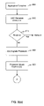
- FIG. 8( a ) and 8 ( b ) illustrate a preferred process for executing an instruction extension in the implicit reconfiguration embodiment of the present invention
- FIG. 9 is a block diagram illustrating the alternating configuration of two ISEF's in accordance with an embodiment of the present invention.
- FIG. 10 is a timing diagram showing the various time phases during alternating configuration of the two ISEF's of FIG. 9 ;
- FIG. 11 is a block diagram illustrating partial Instruction Set Extension Fabric reconfiguration in accordance with the present invention.
- the present invention provides a method for extending a processor instruction set to include new, extended instructions and for replacing a critical code segment of a computer program with a function that causes the new instruction to execute.
- general purpose processors typically do not have programmable instruction sets, the present invention will be described with reference to the programmable processing hardware of FIG. 1 , though it will be appreciated that the invention is not so limited and can be used in conjunction with other suitable programmable processing hardware.
- FIG. 1 is a schematic drawing of an exemplary programmable processing system 110 in an exemplary implementation of the invention.
- the programmable processing system includes a processor core 120 , an Instruction Set Extension Fabric (ISEF) 130 , and an extension adapter 140 that couples the ISEF 130 to the processor core 120 .
- the processor core 120 can include optional features such as coprocessors, write buffers, exception handling features, debug handling features, read only memory (ROM), etc.
- the processor core 120 can include multiple processor cores.
- the processor core 120 provides standard processing capabilities such as a standard (native) instruction set that provides a set of instructions that the processor core 120 is designed to recognize and execute.
- Typical instructions include arithmetic functions such as add, subtract, and multiply, as well as load instructions, store instructions, and so forth. These instructions are hard-coded into the silicon and cannot be modified.
- a suitable processor core 120 is the Xtensa® V (T1050) processor, from Tensilica, Inc., of Santa Clara, Calif.
- Instruction Set Extension Fabric (ISEF) 130 includes programmable logic for enabling application-specific instructions (“instruction extensions”) to be stored and executed.
- the Instruction Set Extension Fabric 130 is a type of programmable logic device. Because it is programmable, the instruction set of Instruction Set Extension Fabric 130 can be readily configured to include instruction extensions that are tailored to a specific application.
- the programmable logic device (ISEF) 130 runs at a slower clock speed than processor core 120 . In these embodiments the cycle length of the programmable logic device 130 can be a multiple of the clock cycle of the processor core 120 .
- Extension adapter 140 provides an interface between the Instruction Set Extension Fabric 130 and the processor core 120 .
- Extension adapter 140 receives instructions and determines whether the instructions should be directed to the Instruction Set Extension Fabric 130 or the processor core 120 .
- extension adapter 140 provides an interface between a plurality of Instruction Set Extension Fabrics 130 and processor cores 120 .
- Extension adapter 140 can be implemented, for example, in Application Specific Integrated Circuit (ASIC) logic.
- extension adapter 140 may be integrated within processor core 120 or ISEF 130 .
- ASIC Application Specific Integrated Circuit
- Extension adapter 140 in combination with ISEF 130 provide logic that allows users to extend the native instruction set defined by the processor core 120 . It is noteworthy that the extended instruction execution itself is implemented in one or more of Instruction Set Extension Fabrics 130 . Extension adapter 140 interfaces one or more Instruction Set Extension Fabrics 130 to one or more processor core 120 and controls dataflow.
- FIG. 2 illustrates one embodiment of an Instruction Set Extension Fabric (ISEF) 130 .
- ISEF 130 includes a plurality of cluster blocks 202 arranged in rows and columns. Data is communicated between cluster blocks 202 by means of a global interconnect 204 .
- the global interconnect 204 also communicates data and dynamic configuration information used or output by ISEF 130 with other devices including extension adapter 140 , which data and dynamic configuration information will be described in more detail below.
- extension adapter 140 which data and dynamic configuration information will be described in more detail below.
- Configuration memory 206 stores static configurations for ISEF 130 .
- the term “memory” is not intended to be construed as limiting. Rather, configuration memory 206 can have various implementations including CMOS static random access memory (SRAM), fused links and slow speed electrically erasable read only memory (EEPROM).
- SRAM CMOS static random access memory
- EEPROM electrically erasable read only memory
- FIG. 3 illustrates a cluster block arrangement that can be used to implement cluster block 202 in FIG. 2 . As shown, it includes a plurality of ALU controller (AC) blocks 302 and function cells 304 . The AC blocks 302 provide configuration signals for a respective column 310 of function cells 304 . In one example of the invention, cluster block 202 includes four columns of four function cells 304 , each column including one AC block 302 .
- AC ALU controller
- FIG. 3 shows paths for sharing data and dynamic configuration information between vertically or horizontally adjacent function cells 304 within cluster block 202 , and with other cluster blocks via global interconnect 204 . Also shown are horizontal word lines 308 and vertical word lines 306 , by which certain or all of the interior function cells 304 may communicate data with other cluster blocks 202 , which word lines partially implement global interconnect 204 .
- Instruction Set Extension Fabric 130 is described in more detail in U.S. Patent Publication Number US 2001/0049816, which is incorporated herein by reference.
- a suitable Instruction Set Extension Fabric 130 is available from Stretch, Inc., of Mountain View, Calif.
- extension adapter 140 comprises load/store module 410 and adapter controller 412 .
- processor core 120 and not extension adapter 140 , comprises load/store module 410 .
- Load/store module 410 can be created via a compiler, such as, for example, the Tensilica Instruction Extension (TIE) compiler, which can be obtained from Tensilica, Inc., of Santa Clara, Calif.
- TIE is a language that allows a user to describe the functionality of new extended instructions.
- a designer uses TIE to create a standard set of functions that extend the normal functionality of processor core 120 .
- the TIE code that a designer writes describes the functionality of a series of resources that aid in the interface between processor core 120 and extension adapter 140 .
- Extension adapter 140 functions such that processor core 120 treats user-defined post-silicon, extended instructions as if they were native instructions to the processor core 120 .
- the extended instruction includes at least one new instruction added post-silicon and a set of pre-silicon instructions.
- Load/store module 410 interfaces with processor core 120 via interface 414 .
- Register file 420 is coupled to interface 414 via processor control and data interface 421 and via ISEF control and data interface 423 .
- Adapter controller 412 interfaces with processor core 120 via interface 416 .
- Adapter controller 412 interfaces with ISEF 130 via interface 418 .
- load/store module 410 comprises register file 420 .
- Register file 420 is a register file, or collections of registers, that is added by using, for example, the TIE compiler.
- Register file 420 interfaces with adapter controller 412 via interface 424 .
- register file 420 is 128 bits wide.
- register file 420 is 64 bits wide.
- register file 420 can be of varying widths. It is contemplated that the system can comprise one or more than one register file 420 .
- Adapter controller 412 accesses register file 420 .
- Adapter controller 412 is then used to interface with ISEF 130 .
- Load/store module 410 provides fixed instruction functionality.
- a set of fixed instructions includes instructions for moving data to and from external memory (not shown), into and out of register file 420 .
- This collection of functionality is defined in one embodiment in the TIE language, and is implemented through Tensilica's TIE compiler. It is contemplated that languages other than TIE can be used with the present system.
- Load/store module 410 contains one or more register files 420 and a set of fixed instructions that give register files 420 access to external memory via load and store instructions. Again, these instructions will be fixed once the silicon is created, and are fully implemented using the standard TIE flow. It is a function of the extension adapter 140 to encapsulate the fixed functionality and manage it with the configurable interface logic.
- a purpose of load/store module 410 includes defining the functionality of register file 420 , which is temporary storage for data that is going to be transferred between processor core 120 and ISEF 130 .
- Load/store module 410 defines not only register file 420 , but also defines how to load and store generic instructions (e.g., Tensilica instructions) of processor core 120 into register file 420 .
- Adapter controller 412 performs the function of interfacing with register file 420 .
- Adapter controller 412 also receives the data from register file 420 and interfaces register file 420 with ISEF 130 .
- standard load and store instructions are used to move data to and from register file 420 .
- Load instructions issued by the extension adapter 140 retrieve data from memory into register file 420 .
- ISEF 130 instructions operate under the control of extension adapter 140 to retrieve stored data from register file 420 to ISEF 130 for use in ISEF 130 computations or other functional execution.
- Data resulting from ISEF 130 instruction execution is then returned to register file 420 , where store instructions move data from register file 420 to memory via interface 414 .
- ISEF 130 and adapter controller 412 allow a user to add new instructions that change with software on different implementations of the same silicon. For example, a user can add specialized instructions to perform video or audio encoding/decoding. These instructions are not hard-wired into processor core 120 , but rather are implemented using the programmably configurable logic of ISEF 130 .
- Extension adapter 140 operates as a data and control interface between processor core 120 and ISEF 130 by routing extended instructions (i.e., those instructions not part of the original processor core 120 native instruction set) to ISEF 130 for execution. Since the logic of ISEF 130 is configurable, it is entirely within the scope of the present invention that the configuration of ISEF 130 can be changed as frequently as needed to accommodate the inclusion of various extended instructions in application programs being run on the processor core 120 .
- the inputs and outputs to the extended instruction, as executed in ISEF 130 are limited to data transfers between a named register file 420 .
- the ISEF 130 can access a register file in the processor core 120 to allow both reading and writing.
- the data transfers are between an alternative source indicative of a processor state.
- this alternative source is a special purpose register.
- the number of register file 420 inputs to the ISEF 130 computation is a finite number such as three (3), and the number of special purpose register inputs is eight (8) 128-bit registers.
- the outputs of the ISEF 130 computations are directed to register file 420 , to equivalent special purpose registers, and/or by-passed to processor core 120 for use in execution of the subsequent instruction.
- the number of register file 420 outputs is two (2) and the number is a 128-bit special purpose register outputs is up to eight (8).
- the extended instruction of such an embodiment does not have direct access to data and instruction memories and caches of the processor core 120 . Any data residing in the data and instruction memories or caches of processor core 120 is first brought into the register file 420 using load instructions, before being used by the extended instruction as executed in ISEF 130 .
- the data residing in the data and instruction memories or caches of processor core 120 are brought into equivalent special purpose registers in addition to the register file 420 using load instructions.
- Such a restriction in the I/O of the extended instruction of this embodiment enables compiler optimization and improved performance.
- the exact input and output dependencies of the extended instructions are programmed into the C compiler (discussed with reference to FIG. 7 ) used in scheduling the extended instruction and in allocating the associated register files 420 .
- extension adapter 140 handles the multiplexing of data among register file(s) 420 and ISEF 130 . Extension adapter 140 manages the timing relationships between register reads and register writes, which are functions of instruction execution length.
- the processing system 110 comprises means for ensuring the proper configuration of ISEF 130 prior to the execution of a specific extended instruction in the ISEF 130 .
- the processing system 110 tries to execute an instruction not included in the instruction set of processor core 120 that is not currently configured in ISEF 130 , an exception is generated by the extension adapter 140 , resulting in either the proper configuration signals being sent to ISEF 130 , or in an alternative process, being initiated to deal with the missing configuration.
- FIG. 5 illustrates an operation involving the reading of data.
- Resident instruction table 510 has a description of what extended instructions are adapted to do with respect to the interface to processor core 120 . For any instruction that a user creates, those instructions should control processor core 120 in such a way that processor core 120 executes those instructions in similar fashion to native instructions included in the original processor core 120 instruction set.
- Resident instruction table 510 receives instruction description data 512 (from interface 414 of FIG. 4 ) as a sequence of binary numbers (e.g., a 24-bit sequence) that is decoded by resident instruction table 510 and converted into an address that points to a location in resident instruction table 510 .
- instruction description data 512 describes a normal add, subtract, etc. contained in the native instruction set of processor core 120 , then resident instruction table 510 does not do anything with the instruction. However, if the instruction description data 512 describes an extended instruction that ISEF 130 is to execute, then resident instruction table 510 returns configuration information 514 back to processor core 120 to indicate this is a valid instruction. Extension adapter 140 will thereafter operate on the extended instruction in cooperation with ISEF 130 so that to processor core 120 it appears that the extended instruction is identical in form to a native instruction of processor core 120 .
- Configuration information 514 is a sequence of data from resident instruction table 510 , some of which goes to processor core 120 via interface 516 . Some of configuration information 514 is transmitted to the ReadAddr 518 (read address) input of register file 420 via interface 424 . Data from ReadData 520 (read data) of register file 220 is also carried on interface 424 . In this example, configuration information 514 includes the address within register file 420 that an extended instruction needs to be sent to ISEF 130 via interface 418 .
- FIG. 6 is a flow chart illustrating an exemplary embodiment 600 of the method of the invention.
- the method begins by defining a program in step 610 .
- the program can be defined in a standard programming language that is familiar to computer programmers such as C++.
- step 620 the program is compiled to convert the program from the programming language in which it was written into a machine language that is recognizable by the processor core 120 ( FIG. 1 ).
- the present method is intended to be iterative, as can be seen from FIG. 6 , and that successive iterations initially return to step 620 .
- a standard compiler such as a C++ compiler
- compiles the program in successive iterations an additional extension compiler is also employed, as is discussed elsewhere herein.
- the extension compiler can be implemented as a separate program or may be part of the compilation phase or linking phase of a standard compiler to perform the operations of the extension compiler as described herein.
- step 630 the compiled program is profiled.
- Profiling includes executing the compiled program with representative or sample data and determining how much time would be expended executing each of the various operations of the program.
- Profiling in step 630 is preferably performed using a software simulation tool (not shown) that mimics the operation of the processor core 120 .
- a software simulation tool (not shown) that mimics the operation of the processor core 120 .
- processor simulators are well known in the art, and each simulator is unique to the processor core 120 being simulated.
- profiling 630 can occur using a hardware emulator (not shown) or some combination of hardware and software. Hardware emulation is particularly useful in applications where specific timing issues are of concern to the designer.
- the first pass through step 630 is different than in successive iterations.
- the compiled program is executed or simulated solely on the processor core 120 to provide a baseline against which improvements in successive iterations can be measured. It should be noted that some of the more time consuming operations that are typically identified by profiling involve nested loops.
- successive programs can take advantage of the existing profiled programs by not performing step 630 .
- a cache can store pre-existing blocks of code, which when matched with the compiled code, results in bypassing step 630 .
- step 640 a determination is made as to the acceptability of the performance of the program. If the performance is acceptable then the method ends. Otherwise, the method continues to step 650 .
- the performance will not be acceptable since no effort has yet been made to optimize the program. In successive iterations, performance can be judged against either subjective or objective standards. In some instances the program needs to be optimized so that it can return data according to the timing requirements of other programs with which it interfaces. In other instances merely a faster processing speed is desired from the program. In these latter instances, at each iteration the performance is compared to the performance from the prior iteration to determine whether the most recent iteration returned a further improvement. If no further improvement is achieved by a successive iteration, or if the improvement is sufficiently trivial, the performance is deemed to be acceptable and the method ends.
- step 650 one or more critical code segments are identified by reviewing the results of the profiling performed in step 630 .
- a critical code segment is a portion of the program's code that took excessive time to execute or failed to meet timing requirements specified for a program in step 630 . Typically, those code segments that took the longest time to execute are considered to be the most critical and are addressed first by the method. As noted elsewhere, nested loops are frequently identified as critical code segments. If addressing the most critical code segments does not produce acceptable performance in step 640 , then in successive iterations the next most critical code segments are identified in step 650 .
- step 660 the critical code segment identified in step 650 is preferably rewritten as a separate function.
- An example is illustrative of this process.
- the following original code segment written in C++ includes a nested loop as the critical code segment:
- markers in C programming, such markers are conventionally referred to as PRAGMAS
- PRAGMAS markers
- the rewriting step of 660 can be performed either manually, or by using an automated conversion tool.
- Such a conversion tool would be similar to a decompiler; rather than compiling a high level instruction into multiple lower level instructions as in a compiler, the automated conversion tool would convert multiple lower level instructions of the processor core 120 instruction set into one or more complex extended instructions for implementation in ISEF 130 .
- step 670 the program is revised.
- the revision includes two operations, designating the function as a code segment to be compiled by an extension compiler and replacing the critical code segment with a statement that calls the function.
- the function is placed into an extensions file, separate from the program file, that contains the code meant to be compiled by the extension compiler.
- the function is placed in the program file and demarked in such a way that it can be recognized as intended for the extension compiler so that the standard compiler will ignore it. Demarking the function in this way can be achieved by a flag before the instruction (e.g., # pragma stretch begin) and a flag after the function (e.g., # pragma stretch end).
- revising the program also includes replacing the critical code segment with a statement that calls the function.
- FIG. 7 illustrates an exemplary sequence of events that occurs during step 620 to compile an extensions file 700 and a program file 710 .
- the code in the extensions file 700 is compiled by the extension compiler 720 .
- An example of an extension compiler 720 is Stretch C, available from Stretch, Inc. of Mountain View, Calif.
- the extension compiler 720 produces two outputs: a header file 730 and an intermediate file 740 written in a hardware description language such as Verilog HDL.
- the header file 730 declares a prototype for a specific function used to execute an extended instruction called out by the extension compiler 720 during compilation of the extensions file 700 .
- the header file 730 is a conventional C file that provides instruction information, such as the file name, inputs required, outputs written, and other required instruction parameters.
- the intermediate file 740 describes how to implement an instruction in the Instruction Set Extension Fabric 130 ( FIG. 1 ) that corresponds to the function.
- an implementation tool 750 maps the intermediate file 740 to the Instruction Set Extension Fabric 130 . More specifically, the implementation tool 750 converts the contents of the intermediate file 740 to ISEF configuration file 760 .
- Implementation tool 750 generates ISEF configuration file 760 consisting of a bit stream that is compiled with program file 710 and header file 730 in standard compiler 770 and incorporated in the executable file 780 .
- This ISEF configuration file 760 contains the data that is used by the executable file 780 to configure ISEF 130 in much the same way that a Field Programmable Gate Array (FPGA) is programmed.
- FPGA Field Programmable Gate Array
- the extension adapter 140 When the extension adapter 140 encounters a processor core 120 instruction that is not part of the native set, but is rather an extended instruction generated by extension compiler 720 , the processor core 120 sends a configuration bit stream to the ISEF 130 to appropriately configure the ISEF 130 to execute the extended instruction.
- the executable file 780 can call the function and the Instruction Set Extension Fabric 130 contains an instruction that can perform the function.
- step 630 the program is again profiled.
- the extension adapter 140 ( FIG. 1 ) directs the Instruction Set Extension Fabric 130 to execute the instruction corresponding to the function when the function is called as the executable file 780 runs. Accordingly, the program executes more efficiently, as will be represented by the profile.
- step 640 the performance is again evaluated, and if acceptable the method ends, otherwise it begins a new iteration at step 650 .
- a critical code segment can alternatively be rewritten by selecting a pre-defined function from a class library.
- the following example is illustrative of pre-defined functions that might be found in a class library according to an embodiment of the present invention, and of an instruction that would be defined from these functions.
- Typical graphics applications define a pixel by an 8-bit integer for each of three colors such as red, green, and blue.
- integers are generally limited to standard bit lengths such as 8, 16, 32 and 64. Accordingly, the ability to create a 24-bit integer, or any integer with a non-standard number of bits, is a beneficial feature of the present invention. Without the ability to define a pixel as a 24-bit integer, one would have to define the pixel as a 32-bit integer, but at the expense of having to carry 8 unused bits.
- a register, W that has a 128-bit width can accommodate four 32-bit pixels, but the same register can handle five 24-bit pixels.
- WR W (P4, P3, P2, P1, P0).
- the processing system 110 uses extended instructions that can be configured into the Instruction Set Extension Fabric 130 to accelerate an executing application program.
- ISEF reconfiguration advantageously can add extension instructions or modify characteristics of existing extension instructions after fabrication of the processor.
- there are no finite limitations on the processing system 110 instruction set since new instruction extensions can be generated by the compiler and configured in the ISEF 130 prior to or during execution of the application. Therefore, the embodiments relating to the configuration of the ISEF 130 to execute non-resident instructions in an application can be thought of as creating a virtual instruction set of the processing system 110 .
- the finite set of instructions can be extended to an unlimited, virtual set of instructions through reconfiguring the ISEF 130 to add new extended instructions. It should be noted that except where reconfiguration does not occur, the term configured and reconfigured are used interchangeably; and that conventionally, the ISEF 130 is initially configured then subsequently reconfigured as explained herein.
- ISEF 130 configuration Several different modes of ISEF 130 configuration are contemplated as varying embodiments.
- the most basic of these embodiments is static configuration, where the instruction extension is loaded with the executable file 780 , and the ISEF 130 is configured once prior to application execution.
- the processor core 120 executes all native instructions, and the instruction extensions are directed to the preconfigured ISEF 130 by the extension adapter 140 for execution.
- the ISEF 130 does not reconfigure during application execution in this static configuration embodiment.
- a second embodiment of ISEF 130 configuration is explicit reconfiguration.
- Explicit reconfiguration is a configuration or reconfiguration of the ISEF 130 in which the executing application program directly initiates the loading of the ISEF 130 configuration memory 206 with instruction extension data in the form of a system call or similar invocation.
- the application preferably prefetches instruction groups before they are required to optimize application execution performance.
- the programmer of the application explicitly adds code to the application to load instruction extension data into the ISEF 130 configuration memory 206 . The added coded includes the system call or similar invocation to initiate the loading of the ISEF 130 configuration memory with the instruction extension data.
- DMA direct memory access
- a third embodiment for configuring the ISEF 130 is that of implicit reconfiguration. Implicit reconfiguration occurs when the running application program issues an instruction, which is not part of the resident instruction set. When a nonresident instruction is issued in this embodiment, the extension adapter 140 detects this instruction fault condition and passes the instruction extension to the ISEF 130 for reconfiguration and execution.
- This model of reconfiguration is referred to as implicit, because the processing system 110 relies on the extension adapter 140 to detect and process the need for the ISEF 130 operation. Programmers of the applications therefore do not need to be aware of the reconfiguration of the ISEF 130 because the reconfiguration does not depend on the programmer-inserted code in the program for reconfiguration. Instead, the reconfiguration of the ISEF 130 occurs when the extension adapter 140 detects the instruction fault condition.
- FIGS. 8( a ) and 8 ( b ) a preferred process is described for executing an instruction extension in the implicit reconfiguration embodiment of the present invention.
- the process of FIGS. 8( a ) and 8 ( b ) begins in step 805 with the execution of a programmed application in the processing system 110 .
- the extension adapter (XAD) 140 receives 810 an instruction extension, i.e. an instruction that is not native to processor core 120 .
- the XAD 140 checks to determine whether the received instruction extension from step 810 is in fact already resident in the ISEF 130 . If the instruction extension is resident, that is currently loaded into ISEF 130 , the ISEF 130 then executes the instruction extension.
- the XAD 140 signals 820 processor core 120 that the instruction extension is not resident. Upon receiving the signal in step 820 from the XAD 140 , processor core 120 issues 825 an instruction fault to the processing system 110 operating system. The processing system 110 operating system then takes steps to appropriately configure the ISEF 130 to execute the received instruction extension in step 810 .
- the XAD 140 is instructed to check 830 whether the ISEF 130 is currently busy executing an instruction. If in fact the ISEF 130 is executing another instruction, then the XAD 140 waits until the ISEF instruction is completed. After any ISEF instruction currently executing completes, then the instruction pipe is flushed 835 and the instruction state is saved in step 840 by the extension adapter XAD 140 . The XAD 140 then loads 845 a new configuration into ISEF 130 and then checks 850 to determine whether a stored state exists relating to the new ISEF 130 configuration of step 845 .
- step 850 If in fact a stored state does exist in step 850 then the XAD 140 restores 855 the state relating to the new ISEF 130 configuration. After any previously stored state is restored, then the XAD 140 reissues 860 the instruction from the application to the ISEF 130 , and the instruction extension executes on the ISEF 130 . Subsequently, application processing resumes in step 865 .
- ISEF 130 reconfiguration a fourth embodiment of ISEF 130 reconfiguration is shown in which two or more ISEF's are alternately configured by an extension adapter 140 .
- Extension adapter 140 is connected to ISEF 1 910 through interconnect 930 .
- Extension adapter 140 likewise is connected to ISEF 2 920 through interconnect 940 .
- multiple groups of instructions may be accelerated and mapped to two or more ISEF's 130 :
- ISEF 1 910 for example, can be executing a set of instruction extensions, while ISEF 2 920 is contemporaneously loading a new reconfiguration file in preparation for a set of instruction extensions to be later executed.
- configuration of one ISEF 130 may overlap execution on the processor core 120 , of another ISEF 130 .
- Execution of instruction extensions may be predicted and speculatively loaded into a ISEF 130 while the application is executing on the processor core 120 or in another ISEF 130 .
- a significant benefit of alternating reconfiguration is that the processing system 110 is able to reduce or avoid delays that might be encountered in ISEF 130 configuration by loading, for example, ISEF 2 920 while the processing system 110 is using ISEF 1 910 for executing an instruction extension. Once the used ISEF 1 910 configuration is completed, processing may then switch to the preconfigured ISEF 2 920 while the contents of ISEF 1 910 are flushed and reprogrammed.
- FIG. 10 a timing diagram is illustrated showing the various timing phases of the processor core 120 and the ISEF's 910 and 920 .
- the processor core 120 is loading 1010 the application within the processing system 110 .
- the application begins execution 1020 on the processor core 120 and starts loading 1025 the first instruction extension into ISEF 1 910 .
- the first instruction extension begins executing 1030 on ISEF 1 910 .
- the application also predicts the next instruction extension to execute, and speculatively loads 1035 the configuration ISEF 2 920 .
- the first instruction extension executing in ISEF 1 910 completes 1045 execution and control returns 1040 to the processor core 120 in phase 4 .
- the second instruction begins execution 1055 on ISEF 2 920 while the next extension instruction is speculatively loaded 1052 into ISEF 1 910 .
- the configuration of ISEF 1 910 runs longer than the execution 1055 of the second instruction extension in ISEF 2 920 in the subsequent instruction extension computation on the processor core 120 , so the application stalls 1060 waiting for the completion of the configuration 1060 at the end of phase 5 .
- the third instruction extension begins execution 1062 on ISEF 1 910 while the fourth extension instruction is predicted and loaded 1065 in ISEF 2 920 .
- the previous prediction is determined 1060 to be incorrect and a new configuration is loaded 1070 into ISEF 2 920 .
- the final loop is executed 1080 on ISEF 2 .
- ISEF 1 130 reconfiguration is a mode in which ISEF 130 is partially configured into two or more Instruction Set Extension Fabrics of equal or differing sizes.
- ISEF 1 1110 may be sized appropriately as needed by a specific instruction extension, and the remainder of ISEF 130 is available for use in the creation and configuration of additional partial ISEF's.
- These partial ISEF's are preferably available for use in the alternating reconfiguration model explained with reference to FIGS. 9 and 10 .
- FIG. 11 shows ISEF 130 divided into two partial ISEF's of equal size, ISEF 130 shown in FIG. 11 could readily be subdivided into any number of sizes and partitions for use in operating with one or more processor cores 120 .
Abstract
Description
- a=0
- for (i=0; i<100; i ++)
- {for (j=0;j<8;j ++)
- {a+=x[i+j]* y[j];}
- z[i]=a>>k;}
The critical code segment can be rewritten as a function, which in the following example is given the name “inner”: - int inner (short*x, short*y)
- {for (j=0; j<8; j ++)
- {a+=x[j]* y[j];}
- return a>>k;}
Advantageously, the function can be written using the same programming language as before. In some embodiments the function does not have to be written from scratch but can instead be selected from a class library (not shown) of pre-defined functions. A class library of pre-defined functions can include functions that might be particularly useful in a certain type of application, such as functions for working with pixel data in video processing applications.
- a=0
- for (i=0; i<100; i ++)
- {z[i]=inner (x+i, y);}
Once the program has been revised instep 670 the method returns to step 620 and the program is again compiled. In those embodiments in which the function has been placed in the program file and demarked from the remaining code, a pre-processing tool first finds the function and copies it out to an extensions file.
Claims (12)
Priority Applications (2)
| Application Number | Priority Date | Filing Date | Title |
|---|---|---|---|
| US11/204,555 US7610475B2 (en) | 2003-07-29 | 2005-08-15 | Programmable logic configuration for instruction extensions |
| US12/561,184 US20100005338A1 (en) | 2003-07-29 | 2009-09-16 | Programmable Logic Configuration for Instruction Extensions |
Applications Claiming Priority (3)
| Application Number | Priority Date | Filing Date | Title |
|---|---|---|---|
| US10/630,542 US7373642B2 (en) | 2003-07-29 | 2003-07-29 | Defining instruction extensions in a standard programming language |
| US10/732,392 US6954845B2 (en) | 2003-07-29 | 2003-12-09 | Reconfigurable instruction set computing |
| US11/204,555 US7610475B2 (en) | 2003-07-29 | 2005-08-15 | Programmable logic configuration for instruction extensions |
Related Parent Applications (1)
| Application Number | Title | Priority Date | Filing Date |
|---|---|---|---|
| US10/732,392 Continuation US6954845B2 (en) | 2003-07-29 | 2003-12-09 | Reconfigurable instruction set computing |
Related Child Applications (1)
| Application Number | Title | Priority Date | Filing Date |
|---|---|---|---|
| US12/561,184 Continuation US20100005338A1 (en) | 2003-07-29 | 2009-09-16 | Programmable Logic Configuration for Instruction Extensions |
Publications (2)
| Publication Number | Publication Date |
|---|---|
| US20050273581A1 US20050273581A1 (en) | 2005-12-08 |
| US7610475B2 true US7610475B2 (en) | 2009-10-27 |
Family
ID=34103868
Family Applications (6)
| Application Number | Title | Priority Date | Filing Date |
|---|---|---|---|
| US10/630,542 Active 2025-04-27 US7373642B2 (en) | 2003-07-29 | 2003-07-29 | Defining instruction extensions in a standard programming language |
| US10/686,882 Active 2024-05-09 US7421561B2 (en) | 2003-07-29 | 2003-10-15 | Instruction set for efficient bit stream and byte stream I/O |
| US10/732,392 Expired - Lifetime US6954845B2 (en) | 2003-07-29 | 2003-12-09 | Reconfigurable instruction set computing |
| US11/099,280 Expired - Lifetime US7284114B2 (en) | 2003-07-29 | 2005-04-04 | Video processing system with reconfigurable instructions |
| US11/204,555 Active 2026-08-10 US7610475B2 (en) | 2003-07-29 | 2005-08-15 | Programmable logic configuration for instruction extensions |
| US12/561,184 Abandoned US20100005338A1 (en) | 2003-07-29 | 2009-09-16 | Programmable Logic Configuration for Instruction Extensions |
Family Applications Before (4)
| Application Number | Title | Priority Date | Filing Date |
|---|---|---|---|
| US10/630,542 Active 2025-04-27 US7373642B2 (en) | 2003-07-29 | 2003-07-29 | Defining instruction extensions in a standard programming language |
| US10/686,882 Active 2024-05-09 US7421561B2 (en) | 2003-07-29 | 2003-10-15 | Instruction set for efficient bit stream and byte stream I/O |
| US10/732,392 Expired - Lifetime US6954845B2 (en) | 2003-07-29 | 2003-12-09 | Reconfigurable instruction set computing |
| US11/099,280 Expired - Lifetime US7284114B2 (en) | 2003-07-29 | 2005-04-04 | Video processing system with reconfigurable instructions |
Family Applications After (1)
| Application Number | Title | Priority Date | Filing Date |
|---|---|---|---|
| US12/561,184 Abandoned US20100005338A1 (en) | 2003-07-29 | 2009-09-16 | Programmable Logic Configuration for Instruction Extensions |
Country Status (2)
| Country | Link |
|---|---|
| US (6) | US7373642B2 (en) |
| WO (1) | WO2005017741A1 (en) |
Cited By (4)
| Publication number | Priority date | Publication date | Assignee | Title |
|---|---|---|---|---|
| US20130301202A1 (en) * | 2012-05-08 | 2013-11-14 | Entegra Technologies, Inc | Reconfigurable Modular Computing Device |
| US9734126B1 (en) | 2016-10-10 | 2017-08-15 | International Business Machines Corporation | Post-silicon configurable instruction behavior based on input operands |
| US10289332B2 (en) * | 2017-04-21 | 2019-05-14 | Arm Limited | Apparatus and method for increasing resilience to faults |
| US10817369B2 (en) | 2017-04-21 | 2020-10-27 | Arm Limited | Apparatus and method for increasing resilience to faults |
Families Citing this family (75)
| Publication number | Priority date | Publication date | Assignee | Title |
|---|---|---|---|---|
| US7613900B2 (en) | 2003-03-31 | 2009-11-03 | Stretch, Inc. | Systems and methods for selecting input/output configuration in an integrated circuit |
| US7581081B2 (en) | 2003-03-31 | 2009-08-25 | Stretch, Inc. | Systems and methods for software extensible multi-processing |
| US7590829B2 (en) * | 2003-03-31 | 2009-09-15 | Stretch, Inc. | Extension adapter |
| US8001266B1 (en) | 2003-03-31 | 2011-08-16 | Stretch, Inc. | Configuring a multi-processor system |
| US7418575B2 (en) * | 2003-07-29 | 2008-08-26 | Stretch, Inc. | Long instruction word processing with instruction extensions |
| US7373642B2 (en) | 2003-07-29 | 2008-05-13 | Stretch, Inc. | Defining instruction extensions in a standard programming language |
| US7237055B1 (en) * | 2003-10-22 | 2007-06-26 | Stretch, Inc. | System, apparatus and method for data path routing configurable to perform dynamic bit permutations |
| US7526632B1 (en) | 2003-10-22 | 2009-04-28 | Stretch, Inc. | System, apparatus and method for implementing multifunctional memory in reconfigurable data path processing |
| US8018463B2 (en) * | 2004-05-10 | 2011-09-13 | Nvidia Corporation | Processor for video data |
| US8130825B2 (en) * | 2004-05-10 | 2012-03-06 | Nvidia Corporation | Processor for video data encoding/decoding |
| US20050289323A1 (en) * | 2004-05-19 | 2005-12-29 | Kar-Lik Wong | Barrel shifter for a microprocessor |
| US7278122B2 (en) * | 2004-06-24 | 2007-10-02 | Ftl Systems, Inc. | Hardware/software design tool and language specification mechanism enabling efficient technology retargeting and optimization |
| US7167971B2 (en) * | 2004-06-30 | 2007-01-23 | International Business Machines Corporation | System and method for adaptive run-time reconfiguration for a reconfigurable instruction set co-processor architecture |
| JP4527571B2 (en) * | 2005-03-14 | 2010-08-18 | 富士通株式会社 | Reconfigurable processing unit |
| US7840000B1 (en) * | 2005-07-25 | 2010-11-23 | Rockwell Collins, Inc. | High performance programmable cryptography system |
| US7539852B2 (en) * | 2005-08-29 | 2009-05-26 | Searete, Llc | Processor resource management |
| US7739524B2 (en) * | 2005-08-29 | 2010-06-15 | The Invention Science Fund I, Inc | Power consumption management |
| US8423824B2 (en) | 2005-08-29 | 2013-04-16 | The Invention Science Fund I, Llc | Power sparing synchronous apparatus |
| US8181004B2 (en) | 2005-08-29 | 2012-05-15 | The Invention Science Fund I, Llc | Selecting a resource management policy for a resource available to a processor |
| US8255745B2 (en) * | 2005-08-29 | 2012-08-28 | The Invention Science Fund I, Llc | Hardware-error tolerant computing |
| US7779213B2 (en) * | 2005-08-29 | 2010-08-17 | The Invention Science Fund I, Inc | Optimization of instruction group execution through hardware resource management policies |
| US7493516B2 (en) * | 2005-08-29 | 2009-02-17 | Searete Llc | Hardware-error tolerant computing |
| US8516300B2 (en) * | 2005-08-29 | 2013-08-20 | The Invention Science Fund I, Llc | Multi-votage synchronous systems |
| US8214191B2 (en) * | 2005-08-29 | 2012-07-03 | The Invention Science Fund I, Llc | Cross-architecture execution optimization |
| US7627739B2 (en) * | 2005-08-29 | 2009-12-01 | Searete, Llc | Optimization of a hardware resource shared by a multiprocessor |
| US20070050608A1 (en) * | 2005-08-29 | 2007-03-01 | Searete Llc, A Limited Liability Corporatin Of The State Of Delaware | Hardware-generated and historically-based execution optimization |
| US7877584B2 (en) * | 2005-08-29 | 2011-01-25 | The Invention Science Fund I, Llc | Predictive processor resource management |
| US8209524B2 (en) * | 2005-08-29 | 2012-06-26 | The Invention Science Fund I, Llc | Cross-architecture optimization |
| US7725693B2 (en) | 2005-08-29 | 2010-05-25 | Searete, Llc | Execution optimization using a processor resource management policy saved in an association with an instruction group |
| US20070050605A1 (en) * | 2005-08-29 | 2007-03-01 | Bran Ferren | Freeze-dried ghost pages |
| US7647487B2 (en) * | 2005-08-29 | 2010-01-12 | Searete, Llc | Instruction-associated processor resource optimization |
| US7653834B2 (en) * | 2005-08-29 | 2010-01-26 | Searete, Llc | Power sparing synchronous apparatus |
| US20070073925A1 (en) * | 2005-09-28 | 2007-03-29 | Arc International (Uk) Limited | Systems and methods for synchronizing multiple processing engines of a microprocessor |
| US20070106883A1 (en) * | 2005-11-07 | 2007-05-10 | Choquette Jack H | Efficient Streaming of Un-Aligned Load/Store Instructions that Save Unused Non-Aligned Data in a Scratch Register for the Next Instruction |
| US7757224B2 (en) * | 2006-02-02 | 2010-07-13 | Microsoft Corporation | Software support for dynamically extensible processors |
| US7870544B2 (en) * | 2006-04-05 | 2011-01-11 | International Business Machines Corporation | Insuring maximum code motion of accesses to DMA buffers |
| US7856545B2 (en) * | 2006-07-28 | 2010-12-21 | Drc Computer Corporation | FPGA co-processor for accelerated computation |
| US7856546B2 (en) * | 2006-07-28 | 2010-12-21 | Drc Computer Corporation | Configurable processor module accelerator using a programmable logic device |
| US7529909B2 (en) * | 2006-12-28 | 2009-05-05 | Microsoft Corporation | Security verified reconfiguration of execution datapath in extensible microcomputer |
| US7971132B2 (en) * | 2007-01-05 | 2011-06-28 | Dialogic Corporation | Universal multimedia engine and method for producing the same |
| US8429623B2 (en) * | 2007-01-16 | 2013-04-23 | Oracle America Inc. | Processing engine for enabling a set of code intended for a first platform to be executed on a second platform |
| US7979674B2 (en) * | 2007-05-16 | 2011-07-12 | International Business Machines Corporation | Re-executing launcher program upon termination of launched programs in MIMD mode booted SIMD partitions |
| US7814295B2 (en) * | 2007-05-18 | 2010-10-12 | International Business Machines Corporation | Moving processing operations from one MIMD booted SIMD partition to another to enlarge a SIMD partition |
| US7831803B2 (en) * | 2007-07-19 | 2010-11-09 | International Business Machines Corporation | Executing multiple instructions multiple date (‘MIMD’) programs on a single instruction multiple data (‘SIMD’) machine |
| US8156307B2 (en) * | 2007-08-20 | 2012-04-10 | Convey Computer | Multi-processor system having at least one processor that comprises a dynamically reconfigurable instruction set |
| US8095735B2 (en) * | 2008-08-05 | 2012-01-10 | Convey Computer | Memory interleave for heterogeneous computing |
| US8122229B2 (en) * | 2007-09-12 | 2012-02-21 | Convey Computer | Dispatch mechanism for dispatching instructions from a host processor to a co-processor |
| US9015399B2 (en) | 2007-08-20 | 2015-04-21 | Convey Computer | Multiple data channel memory module architecture |
| US9710384B2 (en) | 2008-01-04 | 2017-07-18 | Micron Technology, Inc. | Microprocessor architecture having alternative memory access paths |
| US8561037B2 (en) * | 2007-08-29 | 2013-10-15 | Convey Computer | Compiler for generating an executable comprising instructions for a plurality of different instruction sets |
| US8176477B2 (en) | 2007-09-14 | 2012-05-08 | International Business Machines Corporation | Method, system and program product for optimizing emulation of a suspected malware |
| US8780128B2 (en) * | 2007-12-17 | 2014-07-15 | Nvidia Corporation | Contiguously packed data |
| US7872523B2 (en) * | 2008-07-01 | 2011-01-18 | Mks Instruments, Inc. | Radio frequency (RF) envelope pulsing using phase switching of switch-mode power amplifiers |
| GB2462860B (en) * | 2008-08-22 | 2012-05-16 | Advanced Risc Mach Ltd | Apparatus and method for communicating between a central processing unit and a graphics processing unit |
| US8205066B2 (en) * | 2008-10-31 | 2012-06-19 | Convey Computer | Dynamically configured coprocessor for different extended instruction set personality specific to application program with shared memory storing instructions invisibly dispatched from host processor |
| US20100115233A1 (en) * | 2008-10-31 | 2010-05-06 | Convey Computer | Dynamically-selectable vector register partitioning |
| US8392895B2 (en) * | 2009-01-13 | 2013-03-05 | Mediatek Inc. | Firmware extension method and firmware builder |
| US8423745B1 (en) | 2009-11-16 | 2013-04-16 | Convey Computer | Systems and methods for mapping a neighborhood of data to general registers of a processing element |
| US9063805B2 (en) | 2009-11-25 | 2015-06-23 | Freescale Semiconductor, Inc. | Method and system for enabling access to functionality provided by resources outside of an operating system environment |
| AT509740B1 (en) | 2010-05-10 | 2012-03-15 | Josef Kraft | HOLSTER FOR RECORDING A HAND FIREARM |
| US8896610B2 (en) * | 2011-02-18 | 2014-11-25 | Texas Instruments Incorporated | Error recovery operations for a hardware accelerator |
| US10430190B2 (en) | 2012-06-07 | 2019-10-01 | Micron Technology, Inc. | Systems and methods for selectively controlling multithreaded execution of executable code segments |
| US9104532B2 (en) | 2012-12-14 | 2015-08-11 | International Business Machines Corporation | Sequential location accesses in an active memory device |
| US8954939B2 (en) * | 2012-12-31 | 2015-02-10 | Microsoft Corporation | Extending a development environment |
| WO2014169477A1 (en) * | 2013-04-19 | 2014-10-23 | 中国科学院自动化研究所 | Processor with polymorphic instruction set architecture |
| CN103235717B (en) * | 2013-04-19 | 2016-04-06 | 中国科学院自动化研究所 | There is the processor of polymorphic instruction set architecture |
| US9720661B2 (en) * | 2014-03-31 | 2017-08-01 | International Businesss Machines Corporation | Selectively controlling use of extended mode features |
| US9658821B2 (en) | 2014-09-29 | 2017-05-23 | International Business Machines Corporation | Single operation array index computation |
| US10503506B2 (en) * | 2015-10-19 | 2019-12-10 | Arm Limited | Apparatus and method for accessing data in a cache in response to an unaligned load instruction |
| RU2659742C1 (en) | 2017-08-17 | 2018-07-03 | Акционерное общество "Лаборатория Касперского" | Method for emulating the execution of files comprising instructions, different from machine instructions |
| US10133871B1 (en) * | 2017-12-13 | 2018-11-20 | Booz Allen Hamilton Inc. | Method and system for identifying functional attributes that change the intended operation of a compiled binary extracted from a target system |
| US10922203B1 (en) * | 2018-09-21 | 2021-02-16 | Nvidia Corporation | Fault injection architecture for resilient GPU computing |
| CN109558169B (en) * | 2018-11-28 | 2023-07-18 | 中国电子科技集团公司第四十七研究所 | Online reconfigurable method for microprocessor instruction set |
| US11030147B2 (en) | 2019-03-27 | 2021-06-08 | International Business Machines Corporation | Hardware acceleration using a self-programmable coprocessor architecture |
| US11392316B2 (en) * | 2019-05-24 | 2022-07-19 | Texas Instruments Incorporated | System and method for predication handling |
Citations (95)
| Publication number | Priority date | Publication date | Assignee | Title |
|---|---|---|---|---|
| US4635261A (en) | 1985-06-26 | 1987-01-06 | Motorola, Inc. | On chip test system for configurable gate arrays |
| US4766569A (en) | 1985-03-04 | 1988-08-23 | Lattice Semiconductor Corporation | Programmable logic array |
| US4766659A (en) | 1986-03-19 | 1988-08-30 | Duane Cronenwett | Method of making a cartridge for use in injecting a liquid into a tree |
| US4893311A (en) | 1988-04-25 | 1990-01-09 | Motorola, Inc. | CMOS implementation of a built-in self test input generator (BISTIG) |
| US5055997A (en) | 1988-01-13 | 1991-10-08 | U.S. Philips Corporation | System with plurality of processing elememts each generates respective instruction based upon portions of individual word received from a crossbar switch |
| EP0507507A2 (en) | 1991-04-02 | 1992-10-07 | AT&T Corp. | Field programmable function element |
| US5247689A (en) | 1985-02-25 | 1993-09-21 | Ewert Alfred P | Parallel digital processor including lateral transfer buses with interrupt switches to form bus interconnection segments |
| US5258668A (en) | 1992-05-08 | 1993-11-02 | Altera Corporation | Programmable logic array integrated circuits with cascade connections between logic modules |
| US5260611A (en) | 1991-09-03 | 1993-11-09 | Altera Corporation | Programmable logic array having local and long distance conductors |
| US5260610A (en) | 1991-09-03 | 1993-11-09 | Altera Corporation | Programmable logic element interconnections for programmable logic array integrated circuits |
| US5274581A (en) | 1992-05-08 | 1993-12-28 | Altera Corporation | Look up table implementation of fast carry for adders and counters |
| US5274782A (en) | 1990-08-27 | 1993-12-28 | International Business Machines Corporation | Method and apparatus for dynamic detection and routing of non-uniform traffic in parallel buffered multistage interconnection networks |
| US5293489A (en) | 1985-01-24 | 1994-03-08 | Nec Corporation | Circuit arrangement capable of centralizing control of a switching network |
| US5299317A (en) | 1989-09-29 | 1994-03-29 | Syracuse University | Method and apparatus for simulating an interconnection network |
| US5343406A (en) | 1989-07-28 | 1994-08-30 | Xilinx, Inc. | Distributed memory architecture for a configurable logic array and method for using distributed memory |
| US5357152A (en) | 1992-11-10 | 1994-10-18 | Infinite Technology Corporation | Logic system of logic networks with programmable selected functions and programmable operational controls |
| US5361373A (en) | 1992-12-11 | 1994-11-01 | Gilson Kent L | Integrated circuit computing device comprising a dynamically configurable gate array having a microprocessor and reconfigurable instruction execution means and method therefor |
| US5414377A (en) | 1992-12-21 | 1995-05-09 | Xilinx, Inc. | Logic block with look-up table for configuration and memory |
| US5426378A (en) | 1994-04-20 | 1995-06-20 | Xilinx, Inc. | Programmable logic device which stores more than one configuration and means for switching configurations |
| US5436574A (en) | 1993-11-12 | 1995-07-25 | Altera Corporation | Universal logic module with arithmetic capabilities |
| US5471628A (en) | 1992-06-30 | 1995-11-28 | International Business Machines Corporation | Multi-function permutation switch for rotating and manipulating an order of bits of an input data byte in either cyclic or non-cyclic mode |
| US5488612A (en) | 1993-10-04 | 1996-01-30 | International Business Machines, Corporation | Method and apparatus for field testing field programmable logic arrays |
| US5517627A (en) | 1992-09-18 | 1996-05-14 | 3Com Corporation | Read and write data aligner and method |
| US5535406A (en) | 1993-12-29 | 1996-07-09 | Kolchinsky; Alexander | Virtual processor module including a reconfigurable programmable matrix |
| US5619665A (en) | 1995-04-13 | 1997-04-08 | Intrnational Business Machines Corporation | Method and apparatus for the transparent emulation of an existing instruction-set architecture by an arbitrary underlying instruction-set architecture |
| US5636224A (en) | 1995-04-28 | 1997-06-03 | Motorola Inc. | Method and apparatus for interleave/de-interleave addressing in data communication circuits |
| US5652875A (en) | 1993-09-27 | 1997-07-29 | Giga Operations Corporation | Implementation of a selected instruction set CPU in programmable hardware |
| US5682493A (en) | 1993-10-21 | 1997-10-28 | Sun Microsystems, Inc. | Scoreboard table for a counterflow pipeline processor with instruction packages and result packages |
| US5684980A (en) | 1992-07-29 | 1997-11-04 | Virtual Computer Corporation | FPGA virtual computer for executing a sequence of program instructions by successively reconfiguring a group of FPGA in response to those instructions |
| US5696956A (en) | 1995-11-08 | 1997-12-09 | Digital Equipment Corporation | Dynamically programmable reduced instruction set computer with programmable processor loading on program number field and program number register contents |
| US5726584A (en) | 1996-03-18 | 1998-03-10 | Xilinx, Inc. | Virtual high density programmable integrated circuit having addressable shared memory cells |
| US5742180A (en) | 1995-02-10 | 1998-04-21 | Massachusetts Institute Of Technology | Dynamically programmable gate array with multiple contexts |
| US5784636A (en) | 1996-05-28 | 1998-07-21 | National Semiconductor Corporation | Reconfigurable computer architecture for use in signal processing applications |
| US5794062A (en) * | 1995-04-17 | 1998-08-11 | Ricoh Company Ltd. | System and method for dynamically reconfigurable computing using a processing unit having changeable internal hardware organization |
| US5819064A (en) | 1995-11-08 | 1998-10-06 | President And Fellows Of Harvard College | Hardware extraction technique for programmable reduced instruction set computers |
| US5822588A (en) | 1995-06-09 | 1998-10-13 | Sun Microsystem, Inc. | System and method for checking the use of synchronization locks in a multi-threaded target program |
| US5828835A (en) | 1995-05-10 | 1998-10-27 | 3Com Corporation | High throughput message passing process using latency and reliability classes |
| US5847578A (en) | 1994-11-01 | 1998-12-08 | Virtual Machine Works | Programmable multiplexing input/output port |
| US5850564A (en) | 1995-05-03 | 1998-12-15 | Btr, Inc, | Scalable multiple level tab oriented interconnect architecture |
| US5920202A (en) | 1997-02-26 | 1999-07-06 | Xilinx, Inc. | Configurable logic element with ability to evaluate five and six input functions |
| US5926036A (en) | 1991-09-03 | 1999-07-20 | Altera Corporation | Programmable logic array circuits comprising look up table implementation of fast carry adders and counters |
| US5943150A (en) | 1996-09-30 | 1999-08-24 | Regents Of The University Of California | Massively parallel processor networks with optical express channels |
| US5956518A (en) | 1996-04-11 | 1999-09-21 | Massachusetts Institute Of Technology | Intermediate-grain reconfigurable processing device |
| US5963050A (en) | 1997-02-26 | 1999-10-05 | Xilinx, Inc. | Configurable logic element with fast feedback paths |
| US5977793A (en) | 1996-10-10 | 1999-11-02 | Altera Corporation | Programmable logic device with hierarchical interconnection resources |
| US5982195A (en) | 1997-02-20 | 1999-11-09 | Altera Corporation | Programmable logic device architectures |
| US5986465A (en) | 1996-04-09 | 1999-11-16 | Altera Corporation | Programmable logic integrated circuit architecture incorporating a global shareable expander |
| US5999734A (en) | 1997-10-21 | 1999-12-07 | Ftl Systems, Inc. | Compiler-oriented apparatus for parallel compilation, simulation and execution of computer programs and hardware models |
| US6026478A (en) | 1997-08-01 | 2000-02-15 | Micron Technology, Inc. | Split embedded DRAM processor |
| US6092174A (en) | 1998-06-01 | 2000-07-18 | Context, Inc. | Dynamically reconfigurable distributed integrated circuit processor and method |
| US6167502A (en) | 1997-10-10 | 2000-12-26 | Billions Of Operations Per Second, Inc. | Method and apparatus for manifold array processing |
| US6219628B1 (en) | 1997-08-18 | 2001-04-17 | National Instruments Corporation | System and method for configuring an instrument to perform measurement functions utilizing conversion of graphical programs into hardware implementations |
| US6237079B1 (en) | 1997-03-30 | 2001-05-22 | Canon Kabushiki Kaisha | Coprocessor interface having pending instructions queue and clean-up queue and dynamically allocating memory |
| US6292388B1 (en) | 2000-06-28 | 2001-09-18 | Adaptive Silicon, Inc. | Efficient and robust random access memory cell suitable for programmable logic configuration control |
| US20010049816A1 (en) | 1999-12-30 | 2001-12-06 | Adaptive Silicon, Inc. | Multi-scale programmable array |
| US6343337B1 (en) | 1998-09-08 | 2002-01-29 | International Business Machines Corporation | Wide shifting in the vector permute unit |
| US6353841B1 (en) | 1997-12-17 | 2002-03-05 | Elixent, Ltd. | Reconfigurable processor devices |
| US6374403B1 (en) | 1999-08-20 | 2002-04-16 | Hewlett-Packard Company | Programmatic method for reducing cost of control in parallel processes |
| US6415424B1 (en) | 1999-11-09 | 2002-07-02 | International Business Machines Corporation | Multiprocessor system with a high performance integrated distributed switch (IDS) controller |
| US6418045B2 (en) | 2000-06-28 | 2002-07-09 | Adaptive Silicon, Inc. | Efficient and robust random access memory cell suitable for programmable logic configuration control |
| US6426648B1 (en) | 1999-12-30 | 2002-07-30 | RUPP CHARLé R. | Carry lookahead for programmable logic array |
| US6467009B1 (en) | 1998-10-14 | 2002-10-15 | Triscend Corporation | Configurable processor system unit |
| US6505241B2 (en) | 1992-06-03 | 2003-01-07 | Network Caching Technology, L.L.C. | Network intermediate node cache serving as proxy to client node to request missing data from server |
| US20030046513A1 (en) | 2001-08-31 | 2003-03-06 | Nec Corporation | Arrayed processor of array of processing elements whose individual operations and mutual connections are variable |
| US6557092B1 (en) | 1999-03-29 | 2003-04-29 | Greg S. Callen | Programmable ALU |
| US20030097546A1 (en) | 2001-11-20 | 2003-05-22 | Richard Taylor | Reconfigurable processor |
| US20030108119A1 (en) | 2001-09-17 | 2003-06-12 | Mohebbi Behzad Barjesteh | Digital signal processor for wireless baseband processing |
| US6622233B1 (en) | 1999-03-31 | 2003-09-16 | Star Bridge Systems, Inc. | Hypercomputer |
| US20030196058A1 (en) | 2002-04-11 | 2003-10-16 | Ramagopal Hebbalalu S. | Memory system for supporting multiple parallel accesses at very high frequencies |
| US20040019765A1 (en) | 2002-07-23 | 2004-01-29 | Klein Robert C. | Pipelined reconfigurable dynamic instruction set processor |
| US6698015B1 (en) | 2000-06-13 | 2004-02-24 | Cisco Technology, Inc. | Apparatus and method for improving performance of critical code execution |
| US6721884B1 (en) | 1999-02-15 | 2004-04-13 | Koninklijke Philips Electronics N.V. | System for executing computer program using a configurable functional unit, included in a processor, for executing configurable instructions having an effect that are redefined at run-time |
| US6721866B2 (en) | 2001-12-21 | 2004-04-13 | Intel Corporation | Unaligned memory operands |
| US6732354B2 (en) | 2002-04-23 | 2004-05-04 | Quicksilver Technology, Inc. | Method, system and software for programming reconfigurable hardware |
| US6744274B1 (en) | 2001-08-09 | 2004-06-01 | Stretch, Inc. | Programmable logic core adapter |
| US6795900B1 (en) | 2000-07-20 | 2004-09-21 | Silicon Graphics, Inc. | Method and system for storing data at input/output (I/O) interfaces for a multiprocessor system |
| US6799236B1 (en) | 2001-11-20 | 2004-09-28 | Sun Microsystems, Inc. | Methods and apparatus for executing code while avoiding interference |
| US20040193852A1 (en) | 2003-03-31 | 2004-09-30 | Johnson Scott D. | Extension adapter |
| US20040208602A1 (en) | 2001-12-01 | 2004-10-21 | James Plante | Free space optical communications link tolerant of atmospheric interference |
| US6817013B2 (en) | 2000-10-04 | 2004-11-09 | International Business Machines Corporation | Program optimization method, and compiler using the same |
| US6831690B1 (en) | 1999-12-07 | 2004-12-14 | Symagery Microsystems, Inc. | Electrical sensing apparatus and method utilizing an array of transducer elements |
| US6857110B1 (en) | 2001-01-30 | 2005-02-15 | Stretch, Inc. | Design methodology for merging programmable logic into a custom IC |
| US6874110B1 (en) | 2000-05-11 | 2005-03-29 | Stretch, Inc. | Apparatus and method for self testing programmable logic arrays |
| US6883084B1 (en) | 2001-07-25 | 2005-04-19 | University Of New Mexico | Reconfigurable data path processor |
| US20050166038A1 (en) | 2002-04-10 | 2005-07-28 | Albert Wang | High-performance hybrid processor with configurable execution units |
| US6954845B2 (en) | 2003-07-29 | 2005-10-11 | Stretch, Inc. | Reconfigurable instruction set computing |
| US6968544B1 (en) | 1999-10-05 | 2005-11-22 | Infineon Technologies Ag | Method for transformation of interface definitions and intermediate format tables thereof |
| US6986127B1 (en) | 2000-10-03 | 2006-01-10 | Tensilica, Inc. | Debugging apparatus and method for systems of configurable processors |
| US6996709B2 (en) | 1998-09-23 | 2006-02-07 | Infineon Technologies Ag | Method for configuring a configurable hardware block by configuring configurable connections provided around a given type of subunit |
| US7000211B2 (en) | 2003-03-31 | 2006-02-14 | Stretch, Inc. | System and method for efficiently mapping heterogeneous objects onto an array of heterogeneous programmable logic resources |
| US7086047B1 (en) | 2002-12-04 | 2006-08-01 | Xilinx, Inc. | Determining hardware generated by high level language compilation through loop optimizations |
| US7178062B1 (en) | 2003-03-12 | 2007-02-13 | Sun Microsystems, Inc. | Methods and apparatus for executing code while avoiding interference |
| US7254142B2 (en) | 2000-10-31 | 2007-08-07 | Metro Packet Systems Inc. | Method of adjusting a bandwidth capacity of a dynamic channel |
| US7269616B2 (en) | 2003-03-21 | 2007-09-11 | Stretch, Inc. | Transitive processing unit for performing complex operations |
| US7412684B2 (en) | 2004-05-28 | 2008-08-12 | Peter Pius Gutberlet | Loop manipulation in a behavioral synthesis tool |
Family Cites Families (16)
| Publication number | Priority date | Publication date | Assignee | Title |
|---|---|---|---|---|
| US166038A (en) * | 1875-07-27 | Improvement in lap-boards | ||
| US541628A (en) * | 1895-06-25 | Nut-lock | ||
| US662233A (en) * | 1900-05-31 | 1900-11-20 | William Haylor | Stovepipe. |
| US2926036A (en) * | 1958-03-27 | 1960-02-23 | Herbert G Wimberley | Fisherman's knot tying tool |
| US4783738A (en) | 1986-03-13 | 1988-11-08 | International Business Machines Corporation | Adaptive instruction processing by array processor having processor identification and data dependent status registers in each processing element |
| JP3100478B2 (en) * | 1992-10-27 | 2000-10-16 | 株式会社トプコン | Laser rotary irradiation device with reciprocating laser scanning system |
| US5247782A (en) * | 1992-11-04 | 1993-09-28 | The Pillsbury Company | Dough cutting and packing apparatus |
| GB9403030D0 (en) | 1994-02-17 | 1994-04-06 | Austin Kenneth | Re-configurable application specific device |
| JPH1145138A (en) * | 1997-07-25 | 1999-02-16 | Mitsubishi Electric Corp | High-speed bus circuit system |
| WO1999057649A2 (en) * | 1998-05-04 | 1999-11-11 | Intermec Ip Corporation | Automatic data collection device having a network communications capability |
| US6282633B1 (en) * | 1998-11-13 | 2001-08-28 | Tensilica, Inc. | High data density RISC processor |
| US6857013B2 (en) * | 1999-01-29 | 2005-02-15 | Intermec Ip.Corp. | Remote anomaly diagnosis and reconfiguration of an automatic data collection device platform over a telecommunications network |
| US6353541B1 (en) * | 1999-10-20 | 2002-03-05 | Micron Pc, Llc | Processor and circuit board retaining apparatus and method |
| US7043659B1 (en) * | 2001-08-31 | 2006-05-09 | Agilent Technologies, Inc. | System and method for flexible processing of management policies for managing network elements |
| US7937559B1 (en) * | 2002-05-13 | 2011-05-03 | Tensilica, Inc. | System and method for generating a configurable processor supporting a user-defined plurality of instruction sizes |
| EP1443417A1 (en) | 2003-01-31 | 2004-08-04 | STMicroelectronics S.r.l. | A reconfigurable signal processor with embedded flash memory device |
-
2003
- 2003-07-29 US US10/630,542 patent/US7373642B2/en active Active
- 2003-10-15 US US10/686,882 patent/US7421561B2/en active Active
- 2003-12-09 US US10/732,392 patent/US6954845B2/en not_active Expired - Lifetime
-
2004
- 2004-04-07 WO PCT/US2004/010655 patent/WO2005017741A1/en active Application Filing
-
2005
- 2005-04-04 US US11/099,280 patent/US7284114B2/en not_active Expired - Lifetime
- 2005-08-15 US US11/204,555 patent/US7610475B2/en active Active
-
2009
- 2009-09-16 US US12/561,184 patent/US20100005338A1/en not_active Abandoned
Patent Citations (99)
| Publication number | Priority date | Publication date | Assignee | Title |
|---|---|---|---|---|
| US5293489A (en) | 1985-01-24 | 1994-03-08 | Nec Corporation | Circuit arrangement capable of centralizing control of a switching network |
| US5247689A (en) | 1985-02-25 | 1993-09-21 | Ewert Alfred P | Parallel digital processor including lateral transfer buses with interrupt switches to form bus interconnection segments |
| US4766569A (en) | 1985-03-04 | 1988-08-23 | Lattice Semiconductor Corporation | Programmable logic array |
| US4635261A (en) | 1985-06-26 | 1987-01-06 | Motorola, Inc. | On chip test system for configurable gate arrays |
| US4766659A (en) | 1986-03-19 | 1988-08-30 | Duane Cronenwett | Method of making a cartridge for use in injecting a liquid into a tree |
| US5055997A (en) | 1988-01-13 | 1991-10-08 | U.S. Philips Corporation | System with plurality of processing elememts each generates respective instruction based upon portions of individual word received from a crossbar switch |
| US4893311A (en) | 1988-04-25 | 1990-01-09 | Motorola, Inc. | CMOS implementation of a built-in self test input generator (BISTIG) |
| US5343406A (en) | 1989-07-28 | 1994-08-30 | Xilinx, Inc. | Distributed memory architecture for a configurable logic array and method for using distributed memory |
| US5299317A (en) | 1989-09-29 | 1994-03-29 | Syracuse University | Method and apparatus for simulating an interconnection network |
| US5274782A (en) | 1990-08-27 | 1993-12-28 | International Business Machines Corporation | Method and apparatus for dynamic detection and routing of non-uniform traffic in parallel buffered multistage interconnection networks |
| EP0507507A2 (en) | 1991-04-02 | 1992-10-07 | AT&T Corp. | Field programmable function element |
| US5260610A (en) | 1991-09-03 | 1993-11-09 | Altera Corporation | Programmable logic element interconnections for programmable logic array integrated circuits |
| US5926036A (en) | 1991-09-03 | 1999-07-20 | Altera Corporation | Programmable logic array circuits comprising look up table implementation of fast carry adders and counters |
| US5260611A (en) | 1991-09-03 | 1993-11-09 | Altera Corporation | Programmable logic array having local and long distance conductors |
| US5274581A (en) | 1992-05-08 | 1993-12-28 | Altera Corporation | Look up table implementation of fast carry for adders and counters |
| US5258668A (en) | 1992-05-08 | 1993-11-02 | Altera Corporation | Programmable logic array integrated circuits with cascade connections between logic modules |
| US6505241B2 (en) | 1992-06-03 | 2003-01-07 | Network Caching Technology, L.L.C. | Network intermediate node cache serving as proxy to client node to request missing data from server |
| US5471628A (en) | 1992-06-30 | 1995-11-28 | International Business Machines Corporation | Multi-function permutation switch for rotating and manipulating an order of bits of an input data byte in either cyclic or non-cyclic mode |
| US5684980A (en) | 1992-07-29 | 1997-11-04 | Virtual Computer Corporation | FPGA virtual computer for executing a sequence of program instructions by successively reconfiguring a group of FPGA in response to those instructions |
| US5517627A (en) | 1992-09-18 | 1996-05-14 | 3Com Corporation | Read and write data aligner and method |
| US5357152A (en) | 1992-11-10 | 1994-10-18 | Infinite Technology Corporation | Logic system of logic networks with programmable selected functions and programmable operational controls |
| US5361373A (en) | 1992-12-11 | 1994-11-01 | Gilson Kent L | Integrated circuit computing device comprising a dynamically configurable gate array having a microprocessor and reconfigurable instruction execution means and method therefor |
| US5414377A (en) | 1992-12-21 | 1995-05-09 | Xilinx, Inc. | Logic block with look-up table for configuration and memory |
| US5652875A (en) | 1993-09-27 | 1997-07-29 | Giga Operations Corporation | Implementation of a selected instruction set CPU in programmable hardware |
| US5488612A (en) | 1993-10-04 | 1996-01-30 | International Business Machines, Corporation | Method and apparatus for field testing field programmable logic arrays |
| US5682493A (en) | 1993-10-21 | 1997-10-28 | Sun Microsystems, Inc. | Scoreboard table for a counterflow pipeline processor with instruction packages and result packages |
| US5436574A (en) | 1993-11-12 | 1995-07-25 | Altera Corporation | Universal logic module with arithmetic capabilities |
| US5535406A (en) | 1993-12-29 | 1996-07-09 | Kolchinsky; Alexander | Virtual processor module including a reconfigurable programmable matrix |
| US5426378A (en) | 1994-04-20 | 1995-06-20 | Xilinx, Inc. | Programmable logic device which stores more than one configuration and means for switching configurations |
| US5847578A (en) | 1994-11-01 | 1998-12-08 | Virtual Machine Works | Programmable multiplexing input/output port |
| US5742180A (en) | 1995-02-10 | 1998-04-21 | Massachusetts Institute Of Technology | Dynamically programmable gate array with multiple contexts |
| US5619665A (en) | 1995-04-13 | 1997-04-08 | Intrnational Business Machines Corporation | Method and apparatus for the transparent emulation of an existing instruction-set architecture by an arbitrary underlying instruction-set architecture |
| US5794062A (en) * | 1995-04-17 | 1998-08-11 | Ricoh Company Ltd. | System and method for dynamically reconfigurable computing using a processing unit having changeable internal hardware organization |
| US5636224A (en) | 1995-04-28 | 1997-06-03 | Motorola Inc. | Method and apparatus for interleave/de-interleave addressing in data communication circuits |
| US5850564A (en) | 1995-05-03 | 1998-12-15 | Btr, Inc, | Scalable multiple level tab oriented interconnect architecture |
| US5828835A (en) | 1995-05-10 | 1998-10-27 | 3Com Corporation | High throughput message passing process using latency and reliability classes |
| US5822588A (en) | 1995-06-09 | 1998-10-13 | Sun Microsystem, Inc. | System and method for checking the use of synchronization locks in a multi-threaded target program |
| US5819064A (en) | 1995-11-08 | 1998-10-06 | President And Fellows Of Harvard College | Hardware extraction technique for programmable reduced instruction set computers |
| US5696956A (en) | 1995-11-08 | 1997-12-09 | Digital Equipment Corporation | Dynamically programmable reduced instruction set computer with programmable processor loading on program number field and program number register contents |
| US5726584A (en) | 1996-03-18 | 1998-03-10 | Xilinx, Inc. | Virtual high density programmable integrated circuit having addressable shared memory cells |
| US5986465A (en) | 1996-04-09 | 1999-11-16 | Altera Corporation | Programmable logic integrated circuit architecture incorporating a global shareable expander |
| US5956518A (en) | 1996-04-11 | 1999-09-21 | Massachusetts Institute Of Technology | Intermediate-grain reconfigurable processing device |
| US5784636A (en) | 1996-05-28 | 1998-07-21 | National Semiconductor Corporation | Reconfigurable computer architecture for use in signal processing applications |
| US5943150A (en) | 1996-09-30 | 1999-08-24 | Regents Of The University Of California | Massively parallel processor networks with optical express channels |
| US5977793A (en) | 1996-10-10 | 1999-11-02 | Altera Corporation | Programmable logic device with hierarchical interconnection resources |
| US5982195A (en) | 1997-02-20 | 1999-11-09 | Altera Corporation | Programmable logic device architectures |
| US5963050A (en) | 1997-02-26 | 1999-10-05 | Xilinx, Inc. | Configurable logic element with fast feedback paths |
| US5920202A (en) | 1997-02-26 | 1999-07-06 | Xilinx, Inc. | Configurable logic element with ability to evaluate five and six input functions |
| US6237079B1 (en) | 1997-03-30 | 2001-05-22 | Canon Kabushiki Kaisha | Coprocessor interface having pending instructions queue and clean-up queue and dynamically allocating memory |
| US6026478A (en) | 1997-08-01 | 2000-02-15 | Micron Technology, Inc. | Split embedded DRAM processor |
| US6219628B1 (en) | 1997-08-18 | 2001-04-17 | National Instruments Corporation | System and method for configuring an instrument to perform measurement functions utilizing conversion of graphical programs into hardware implementations |
| US6167502A (en) | 1997-10-10 | 2000-12-26 | Billions Of Operations Per Second, Inc. | Method and apparatus for manifold array processing |
| US5999734A (en) | 1997-10-21 | 1999-12-07 | Ftl Systems, Inc. | Compiler-oriented apparatus for parallel compilation, simulation and execution of computer programs and hardware models |
| US6353841B1 (en) | 1997-12-17 | 2002-03-05 | Elixent, Ltd. | Reconfigurable processor devices |
| US6092174A (en) | 1998-06-01 | 2000-07-18 | Context, Inc. | Dynamically reconfigurable distributed integrated circuit processor and method |
| US6343337B1 (en) | 1998-09-08 | 2002-01-29 | International Business Machines Corporation | Wide shifting in the vector permute unit |
| US6996709B2 (en) | 1998-09-23 | 2006-02-07 | Infineon Technologies Ag | Method for configuring a configurable hardware block by configuring configurable connections provided around a given type of subunit |
| US6467009B1 (en) | 1998-10-14 | 2002-10-15 | Triscend Corporation | Configurable processor system unit |
| US6721884B1 (en) | 1999-02-15 | 2004-04-13 | Koninklijke Philips Electronics N.V. | System for executing computer program using a configurable functional unit, included in a processor, for executing configurable instructions having an effect that are redefined at run-time |
| US6557092B1 (en) | 1999-03-29 | 2003-04-29 | Greg S. Callen | Programmable ALU |
| US6622233B1 (en) | 1999-03-31 | 2003-09-16 | Star Bridge Systems, Inc. | Hypercomputer |
| US6374403B1 (en) | 1999-08-20 | 2002-04-16 | Hewlett-Packard Company | Programmatic method for reducing cost of control in parallel processes |
| US6968544B1 (en) | 1999-10-05 | 2005-11-22 | Infineon Technologies Ag | Method for transformation of interface definitions and intermediate format tables thereof |
| US6415424B1 (en) | 1999-11-09 | 2002-07-02 | International Business Machines Corporation | Multiprocessor system with a high performance integrated distributed switch (IDS) controller |
| US6831690B1 (en) | 1999-12-07 | 2004-12-14 | Symagery Microsystems, Inc. | Electrical sensing apparatus and method utilizing an array of transducer elements |
| US6426648B1 (en) | 1999-12-30 | 2002-07-30 | RUPP CHARLé R. | Carry lookahead for programmable logic array |
| US7062520B2 (en) | 1999-12-30 | 2006-06-13 | Stretch, Inc. | Multi-scale programmable array |
| US6633181B1 (en) | 1999-12-30 | 2003-10-14 | Stretch, Inc. | Multi-scale programmable array |
| US20010049816A1 (en) | 1999-12-30 | 2001-12-06 | Adaptive Silicon, Inc. | Multi-scale programmable array |
| US6874110B1 (en) | 2000-05-11 | 2005-03-29 | Stretch, Inc. | Apparatus and method for self testing programmable logic arrays |
| US6698015B1 (en) | 2000-06-13 | 2004-02-24 | Cisco Technology, Inc. | Apparatus and method for improving performance of critical code execution |
| US6292388B1 (en) | 2000-06-28 | 2001-09-18 | Adaptive Silicon, Inc. | Efficient and robust random access memory cell suitable for programmable logic configuration control |
| US6418045B2 (en) | 2000-06-28 | 2002-07-09 | Adaptive Silicon, Inc. | Efficient and robust random access memory cell suitable for programmable logic configuration control |
| US6795900B1 (en) | 2000-07-20 | 2004-09-21 | Silicon Graphics, Inc. | Method and system for storing data at input/output (I/O) interfaces for a multiprocessor system |
| US6986127B1 (en) | 2000-10-03 | 2006-01-10 | Tensilica, Inc. | Debugging apparatus and method for systems of configurable processors |
| US6817013B2 (en) | 2000-10-04 | 2004-11-09 | International Business Machines Corporation | Program optimization method, and compiler using the same |
| US7254142B2 (en) | 2000-10-31 | 2007-08-07 | Metro Packet Systems Inc. | Method of adjusting a bandwidth capacity of a dynamic channel |
| US6857110B1 (en) | 2001-01-30 | 2005-02-15 | Stretch, Inc. | Design methodology for merging programmable logic into a custom IC |
| US6883084B1 (en) | 2001-07-25 | 2005-04-19 | University Of New Mexico | Reconfigurable data path processor |
| US6744274B1 (en) | 2001-08-09 | 2004-06-01 | Stretch, Inc. | Programmable logic core adapter |
| US7350054B2 (en) | 2001-08-31 | 2008-03-25 | Nec Corporation | Processor having array of processing elements whose individual operations and mutual connections are variable |
| US20030046513A1 (en) | 2001-08-31 | 2003-03-06 | Nec Corporation | Arrayed processor of array of processing elements whose individual operations and mutual connections are variable |
| US20030108119A1 (en) | 2001-09-17 | 2003-06-12 | Mohebbi Behzad Barjesteh | Digital signal processor for wireless baseband processing |
| US6799236B1 (en) | 2001-11-20 | 2004-09-28 | Sun Microsystems, Inc. | Methods and apparatus for executing code while avoiding interference |
| US20030097546A1 (en) | 2001-11-20 | 2003-05-22 | Richard Taylor | Reconfigurable processor |
| US20040208602A1 (en) | 2001-12-01 | 2004-10-21 | James Plante | Free space optical communications link tolerant of atmospheric interference |
| US6721866B2 (en) | 2001-12-21 | 2004-04-13 | Intel Corporation | Unaligned memory operands |
| US20050166038A1 (en) | 2002-04-10 | 2005-07-28 | Albert Wang | High-performance hybrid processor with configurable execution units |
| US20030196058A1 (en) | 2002-04-11 | 2003-10-16 | Ramagopal Hebbalalu S. | Memory system for supporting multiple parallel accesses at very high frequencies |
| US6732354B2 (en) | 2002-04-23 | 2004-05-04 | Quicksilver Technology, Inc. | Method, system and software for programming reconfigurable hardware |
| US20040019765A1 (en) | 2002-07-23 | 2004-01-29 | Klein Robert C. | Pipelined reconfigurable dynamic instruction set processor |
| US7086047B1 (en) | 2002-12-04 | 2006-08-01 | Xilinx, Inc. | Determining hardware generated by high level language compilation through loop optimizations |
| US7178062B1 (en) | 2003-03-12 | 2007-02-13 | Sun Microsystems, Inc. | Methods and apparatus for executing code while avoiding interference |
| US7269616B2 (en) | 2003-03-21 | 2007-09-11 | Stretch, Inc. | Transitive processing unit for performing complex operations |
| US7000211B2 (en) | 2003-03-31 | 2006-02-14 | Stretch, Inc. | System and method for efficiently mapping heterogeneous objects onto an array of heterogeneous programmable logic resources |
| US20040193852A1 (en) | 2003-03-31 | 2004-09-30 | Johnson Scott D. | Extension adapter |
| US6954845B2 (en) | 2003-07-29 | 2005-10-11 | Stretch, Inc. | Reconfigurable instruction set computing |
| US7373642B2 (en) | 2003-07-29 | 2008-05-13 | Stretch, Inc. | Defining instruction extensions in a standard programming language |
| US7412684B2 (en) | 2004-05-28 | 2008-08-12 | Peter Pius Gutberlet | Loop manipulation in a behavioral synthesis tool |
Non-Patent Citations (48)
| Title |
|---|
| "MIPS Extension for Digital Media with 3D," MIPS Technologies, Inc., Dec. 27, 1996. |
| Barat Francisco et al. "Reconfigurable Instruction Set Processors: A Survey" IEEE 2000 0-7695-0688-2/00. |
| Bechade et al., "Programmable Arithmetic/Logic Circuits," IBM Technical Disclosure Bulletin, U.S. IBM Corp., New York, vol. 3, No. 11, Apr. 1981, pp. 4870-4873, XP-000713711. |
| Bechade, R. A. et al., "Programmable Arithmetic/Logic Circuits," IBM Technical Disclosure Bulletin, U.S. IBM Corp., New York, vol. 3, No. 11, Apr. 1981, pp. 4870-4873, XP-000713711. |
| Beeck et al., "CRISP: A Template for Reconfigurable Instruction Set Processors," FPL 2001, LNCS 2147, pp. 296-305, Springer-Verlag Berlin Heidelberg, 2001. |
| Borgatti, M. et al., "A Reconfigurable System Featureing Dynamically Extensible Embedded Microprocessor, FPGA and Customisable I/O," IEEE 2002 Custom Integrated Circuits Conference, 2002, pp. 1-4. |
| Borgatti, Michele et al., "A Reconfigurable System featuring Dynamically Extensible Embedded Microprocessor, FPGA and Customisable I/O," 2002, IEEE Custom Integrated Circuits Conference, pp. 1-4. |
| Borkar Shekhar et al. "iWarp: An Integrated Solution to High-Speed Parallel Computing" IEEE 1998 pp. 330-339. |
| Carrillo et al.; "The Effect of Reconfigurable Units in Superscalar Processors" 2001; ACM. |
| Dally, William J. and Charles L. Seitz, "Deadlock Free Message Routing in Multiprocessor Interconnection Networks," May 10, 1985, Computer Science Department, California Institute of Technology. |
| DeHon, Andre, "Transit Note #118 Notes on Coupling Processors with Reconfigurable Logic," M.I.T. Transit Project, Last Updated Mar. 21, 1995. |
| Diniz et al. "Automatic Synthesis of Data Storage and Control Structures for FPGA-based Computing Engines" 2000 IEEE pp. 91-100. |
| Garlan, David and Mary Shaw, "An Introduction to Software Architecture," Jan. 1994, CMU-CS-94-166, School of Computer Science, Carnegie Mellon University, Pittsburgh, PA. |
| Goldblatt, Kim, "The Low-Cost, Efficient Serial Configuration of Spartan FPGAs," Nov. 13, 1998, XAPP098 (Version 1.0), Xilinx. |
| Golestani, S. Jamaloddin, "A Sto-and-Go Queuing Framework for Congestion Management," 1990, Proc. of the ACM Symposium on Communications Architectures & Protocols, ACM Press, New York, NY, pp. 8-18. |
| Gonzalez "Xtensa: A Configurable and Extensible Processor" Mar.-Apr. 2000 IEEE Micro pp. 60-70. |
| Hauck et al., "The Chimaera Reconfigurable Functional Unit", Proceedings of the 5th Annual Symposium on FPGAs for Custom Computing Machines, Apr. 16-18, 1997, IEEE, pp. 87-96. * |
| Hennessy, John L. and David A. Patterson, "Computer Organization and Design: The Hardware/Software Interface," 1998, 2nd edition, Morgan Kaufmann Publishers, Inc., San Francisco, CA, p. 345. |
| http://www.tensilica.com/products/xtensa-overview.htm Xtensa Processor Overview. |
| Hwang, Kai, "Advanced Computer Architecture: Parallelism, Scalability, Programmability," 1993, McGraw Hill, pp. 182-183. |
| Intel and Hewlett-Packard, "IA-64 Application Instruction Set Architecture Guide," Revision 1.0, 1999, pp. C-1 through C. |
| Jacob et al; "Memory Interfacing and Instruction Specification ofr Reconfigurable Processors" 1999; ACM. |
| Lee, K.C., "A Virtual Bus Architecture for Dynamic Parallel Processing," Feb. 1993, IEEE Transactions on Parallel and Undistributed Systems, vol. 4, No. 2, pp. 121-130. |
| Lu et al., "The MorphoSys Dynamically Reconfigurable System-On-Chip", Proceedings of the First NASA/DoD Workshop on Evolvable Hardware, IEEE, Jul. 19-22, 1999, pp. 152-160. * |
| Michael J. Wirthlin et al., "DISC: The dynamic instruction set computer," Proceedings SPIE, Field Programmable Gate Arrays (FPGAs) for Fast Board Development and Reconfigurable Computing, Oct. 25-26, 1995, 14 pages. |
| MIPS Technologies, Inc., "MIPS Extension for Digital Media with 3D," 1996, pp. 1-26. |
| Razdan, R. et al., "A High-Performance Microarchitecture with Hardware-Programmable Functional Units," Proc. of Micro-27, Nov. 1994. |
| Razdan, Rahul and Michael D. Smith, "A High-Performance Michroarchitecture with Hardware-Programmable Functional Units," Nov. 1994, Proc. of Micro-27, pp. 1-9. |
| Rupp et al.; U.S. Appl. No. 10/746,018 entitled "Architecture and Method for Reconfigurable Data Path Processing" filed Dec. 23 2003. |
| Scott, Steven L. and Gregory M. Thorson, "The Cray T3E Network: Adaptive Routing in a High Performance 3D Torus," Aug. 15-16, 1996, Hot Interconnects IV, Stanford University. |
| Tanenbaum, Andrew S., "Modern Operating Systems," 2001, 2nd edition, Prentice Hall, New Jersey, p. 31. |
| Taylor Michael Bedford et al. "The Raw Microprocessor: A Computational Fabric for Software Circuits and General-Purpose Programs" Microarchitecture IEEE Micro Mar.-Apr. 2002 pp. 25-35. |
| U.S. Appl. No. 10/394,824, Charle' Rupp, Transitive Processing Unit for Performing Complex Operations, filed Mar. 21, 2003. |
| U.S. Appl. No. 10/404,706, Scott D. Johnson, Extension Adapter, filed Mar. 31, 2003. |
| U.S. Appl. No. 10/630,542, Albert Wang, Defining Instruction Extensions in a Standard Programming Language, filed Jul. 29, 2003. |
| U.S. Appl. No. 10/630,542, Kenneth Williams, Defining Instruction Extensions in a Standard Programming Language, filed Jul. 29, 2003. |
| U.S. Appl. No. 10/686,882, Kenneth Williams, Instruction Set for Efficient Bit Stream and Byte Stream I/O, filed Oct. 15, 2003. |
| U.S. Appl. No. 10/750,714, Ricardo Gonzalez, Systems and Methods for Software Extensible Multi-Processing, filed Dec. 31, 2003. |
| U.S. Appl. No. 10/815,453, Ricardo Gonzalez, Configuring a Multi-Processor System, filed Mar. 31, 2004. |
| U.S. Appl. No. 11/021,247, Ricardo Gonzalez, Systems and Methods for Selecting Input/Output Configuration in an Integrated Circuit, filed Dec. 21, 2004. |
| U.S. Appl. No. 11/099,280, Jeffrey M. Arnold, Video Processing System with Reconfigurable Instructions, filed Apr. 4, 2005. |
| U.S. Appl. No. 11/099,280, Jeffrey Mark Arnold, Video Processing System with Reconfigurable Instructions, filed Apr. 4, 2005. |
| U.S. Appl. No. 11/129,146, Ricardo Gonzalez, Long Instruction Word Processing with Instruction Extensions, filed May 12, 2005. |
| U.S. Appl. No. 11/204,555, Jeffrey M. Arnold, Programmable Logic Configuration for Instruction Extensions, filed Aug. 15, 2005. |
| Waingold Elliot et al. "Baring It All to Software: Raw Machines" Computer Sep. 1997 IEEE pp. 86-93. |
| Xilinx, "Virtex(TM) 2.5 V Field Programmable Gate Arrays, Product Specification," DS003-2 (v2.8.1) Dec. 9, 2002, pp. 1-20. |
| Ye et al., "CHIMAERA: A High-Performance Architecture with a Tightly-Coupled Reconfigurable Functional Unit", Proceedings of the 27th International Symposium on Computer Architecture, IEEE, Jun. 10-14, 2000, pp. 225-235. |
| Ye, Z.A. et al., "CHIMAERA: a high-performance architecture with a tightly-coupled reconfigurable functional unit," Jun. 10-14, 2000, Proc. of the 27th International Symposium on Computer Architecture, pp. 225-235. |
Cited By (7)
| Publication number | Priority date | Publication date | Assignee | Title |
|---|---|---|---|---|
| US20130301202A1 (en) * | 2012-05-08 | 2013-11-14 | Entegra Technologies, Inc | Reconfigurable Modular Computing Device |
| US8751710B2 (en) * | 2012-05-08 | 2014-06-10 | Entegra Technologies, Inc. | Reconfigurable modular computing device |
| US8924609B2 (en) | 2012-05-08 | 2014-12-30 | Entegra Technologies, Inc. | Reconfigurable modular computing device |
| US9213664B2 (en) | 2012-05-08 | 2015-12-15 | Entegra Technologies, Inc. | Reconfigurable modular computing device |
| US9734126B1 (en) | 2016-10-10 | 2017-08-15 | International Business Machines Corporation | Post-silicon configurable instruction behavior based on input operands |
| US10289332B2 (en) * | 2017-04-21 | 2019-05-14 | Arm Limited | Apparatus and method for increasing resilience to faults |
| US10817369B2 (en) | 2017-04-21 | 2020-10-27 | Arm Limited | Apparatus and method for increasing resilience to faults |
Also Published As
| Publication number | Publication date |
|---|---|
| US20050273581A1 (en) | 2005-12-08 |
| US20100005338A1 (en) | 2010-01-07 |
| US7421561B2 (en) | 2008-09-02 |
| US7284114B2 (en) | 2007-10-16 |
| US20050027970A1 (en) | 2005-02-03 |
| US20050027944A1 (en) | 2005-02-03 |
| US7373642B2 (en) | 2008-05-13 |
| US6954845B2 (en) | 2005-10-11 |
| US20050027971A1 (en) | 2005-02-03 |
| WO2005017741A1 (en) | 2005-02-24 |
| US20050169550A1 (en) | 2005-08-04 |
Similar Documents
| Publication | Publication Date | Title |
|---|---|---|
| US7610475B2 (en) | Programmable logic configuration for instruction extensions | |
| US8321849B2 (en) | Virtual architecture and instruction set for parallel thread computing | |
| US6077315A (en) | Compiling system and method for partially reconfigurable computing | |
| Cronquist et al. | Specifying and compiling applications for RaPiD | |
| US8448150B2 (en) | System and method for translating high-level programming language code into hardware description language code | |
| KR101082797B1 (en) | System and Method for translating high-level programming language code into Hardware Description Language code | |
| TWI806550B (en) | Processor operation method, related computer system, and non-transitory computer-accessible storage medium | |
| US20070129926A1 (en) | Hardware acceleration system for simulation of logic and memory | |
| Yu et al. | Vector processing as a soft-core CPU accelerator | |
| JPH10320214A (en) | Compile system and computer program product | |
| US10733343B2 (en) | System and method for the design of digital hardware | |
| WO2002061631A2 (en) | System, method and article of manufacture for using a library map to create and maintain ip cores effectively | |
| JP2008276740A5 (en) | ||
| JP2009533785A (en) | Branching and behavior splitting for VLIW processors | |
| JP2002024011A (en) | Described execution of instruction in processor | |
| Lanzagorta et al. | Introduction to reconfigurable supercomputing | |
| Stitt et al. | Techniques for synthesizing binaries to an advanced register/memory structure | |
| Zaretsky et al. | Overview of the FREEDOM compiler for mapping DSP software to FPGAs | |
| Gokhale et al. | Malleable architecture generator for FPGA computing | |
| Tanaka et al. | A code selection method for SIMD processors with PACK instructions | |
| Terechko et al. | PRMDL: a machine description language for clustered VLIW architectures. | |
| Vanderbauwhede et al. | MORA: High-Level FPGA Programming Using a Many-Core Framework | |
| Kenyon et al. | High-level microprogramming: an optimizing C compiler for a processing element of a CAD accelerator | |
| Bell et al. | Computations and Compilers | |
| US20050080957A1 (en) | Controller based hardware device and method for setting the same |
Legal Events
| Date | Code | Title | Description |
|---|---|---|---|
| AS | Assignment |
Owner name: STRETCH, INC., CALIFORNIA Free format text: ASSIGNMENT OF ASSIGNORS INTEREST;ASSIGNORS:ARNOLD, JEFFREY MARK;BANTA, GARELD HOWARD;JOHNSON, SCOTT DANIEL;AND OTHERS;REEL/FRAME:016875/0875 Effective date: 20031209 |
|
| STCF | Information on status: patent grant |
Free format text: PATENTED CASE |
|
| CC | Certificate of correction | ||
| AS | Assignment |
Owner name: SILICON VALLEY BANK, CALIFORNIA Free format text: SECURITY AGREEMENT;ASSIGNOR:STRETCH, INC.;REEL/FRAME:025413/0831 Effective date: 20101122 |
|
| AS | Assignment |
Owner name: MMV FINANCE INC., CANADA Free format text: SECURITY AGREEMENT;ASSIGNOR:STRETCH, INC.;REEL/FRAME:029591/0364 Effective date: 20101122 |
|
| FPAY | Fee payment |
Year of fee payment: 4 |
|
| FEPP | Fee payment procedure |
Free format text: PAT HOLDER CLAIMS SMALL ENTITY STATUS, ENTITY STATUS SET TO SMALL (ORIGINAL EVENT CODE: LTOS); ENTITY STATUS OF PATENT OWNER: LARGE ENTITY |
|
| AS | Assignment |
Owner name: STRETCH, INC., CALIFORNIA Free format text: RELEASE OF SECURITY INTEREST IN PATENTS;ASSIGNOR:MMV CAPITAL PARTNERS INC., AS ASSIGNEE OF MMV FINANCE INC.;REEL/FRAME:032037/0551 Effective date: 20140114 Owner name: STRETCH, INC., CALIFORNIA Free format text: RELEASE OF SECURITY INTEREST IN PATENTS;ASSIGNOR:SILICON VALLEY BANK;REEL/FRAME:032037/0527 Effective date: 20140114 |
|
| AS | Assignment |
Owner name: EXAR CORPORATION, CALIFORNIA Free format text: ACQUISITION;ASSIGNOR:STRETCH, INC.;REEL/FRAME:032301/0591 Effective date: 20140114 |
|
| AS | Assignment |
Owner name: STIFEL FINANCIAL CORP., MISSOURI Free format text: SECURITY INTEREST;ASSIGNORS:EXAR CORPORATION;CADEKA MICROCIRCUITS, LLC;REEL/FRAME:033062/0123 Effective date: 20140527 |
|
| FEPP | Fee payment procedure |
Free format text: PAT HOLDER NO LONGER CLAIMS SMALL ENTITY STATUS, ENTITY STATUS SET TO UNDISCOUNTED (ORIGINAL EVENT CODE: STOL); ENTITY STATUS OF PATENT OWNER: LARGE ENTITY |
|
| AS | Assignment |
Owner name: EXAR CORPORATION, CALIFORNIA Free format text: RELEASE BY SECURED PARTY;ASSIGNOR:STIFEL FINANCIAL CORP.;REEL/FRAME:035168/0384 Effective date: 20150309 Owner name: CADEKA MICROCIRCUITS, LLC, COLORADO Free format text: RELEASE BY SECURED PARTY;ASSIGNOR:STIFEL FINANCIAL CORP.;REEL/FRAME:035168/0384 Effective date: 20150309 |
|
| AS | Assignment |
Owner name: XILINX, INC., CALIFORNIA Free format text: ASSIGNMENT OF ASSIGNORS INTEREST;ASSIGNOR:EXAR CORPORATION;REEL/FRAME:036416/0211 Effective date: 20150626 |
|
| FPAY | Fee payment |
Year of fee payment: 8 |
|
| MAFP | Maintenance fee payment |
Free format text: PAYMENT OF MAINTENANCE FEE, 12TH YEAR, LARGE ENTITY (ORIGINAL EVENT CODE: M1553); ENTITY STATUS OF PATENT OWNER: LARGE ENTITY Year of fee payment: 12 |