US7608211B2 - Method of making a liquid crystal display device - Google Patents
Method of making a liquid crystal display device Download PDFInfo
- Publication number
- US7608211B2 US7608211B2 US11/330,156 US33015606A US7608211B2 US 7608211 B2 US7608211 B2 US 7608211B2 US 33015606 A US33015606 A US 33015606A US 7608211 B2 US7608211 B2 US 7608211B2
- Authority
- US
- United States
- Prior art keywords
- photo
- liquid crystal
- alignment
- group
- alignment layer
- Prior art date
- Legal status (The legal status is an assumption and is not a legal conclusion. Google has not performed a legal analysis and makes no representation as to the accuracy of the status listed.)
- Expired - Fee Related, expires
Links
- QVLGLUNWUYAHBB-TYICYAFGSA-N C.C.CO[C@@H]1O[C@H](C)[C@@H](O[C@@H]2O[C@H](C)C(C)[C@H](C)[C@H]2C)[C@H](C)[C@H]1C Chemical compound C.C.CO[C@@H]1O[C@H](C)[C@@H](O[C@@H]2O[C@H](C)C(C)[C@H](C)[C@H]2C)[C@H](C)[C@H]1C QVLGLUNWUYAHBB-TYICYAFGSA-N 0.000 description 3
- FVHXHWBSYGFICC-UHFFFAOYSA-N CC.CC.CC(=O)C=Cc1ccc(-c2ccc([Y])cc2)cc1 Chemical compound CC.CC.CC(=O)C=Cc1ccc(-c2ccc([Y])cc2)cc1 FVHXHWBSYGFICC-UHFFFAOYSA-N 0.000 description 3
- 0 *O[C@@H]1O[C@H](C)[C@@H](O[C@@H]2O[C@H](C)[C@@H](C)[C@H](C)[C@H]2C)[C@H](C)[C@H]1C.C.C.C.C.C.C=O(CO)[C@@H]1O[C@H](CCO)[C@@H](O[C@@H]2O[C@H](COCCO)[C@@]3(OC3CO)[C@H](CCO)[C@H]2CCO)[C@H](CCO)[C@H]1CCO.CC.CC.CC.CC.CC.CC.CC.CC.CCCOC(=O)C=CC1=CC=C(C2=CC=C([Y])C=C2)C=C1.O=C(Cl)C=Cc1ccc(-c2ccc([Y])cc2)cc1.O=C(O)C=Cc1ccc(-c2ccc([Y])cc2)cc1.O=C(O)CC(=O)O.O=Cc1ccc(-c2ccc([Y])cc2)cc1.O=S(Cl)Cl Chemical compound *O[C@@H]1O[C@H](C)[C@@H](O[C@@H]2O[C@H](C)[C@@H](C)[C@H](C)[C@H]2C)[C@H](C)[C@H]1C.C.C.C.C.C.C=O(CO)[C@@H]1O[C@H](CCO)[C@@H](O[C@@H]2O[C@H](COCCO)[C@@]3(OC3CO)[C@H](CCO)[C@H]2CCO)[C@H](CCO)[C@H]1CCO.CC.CC.CC.CC.CC.CC.CC.CC.CCCOC(=O)C=CC1=CC=C(C2=CC=C([Y])C=C2)C=C1.O=C(Cl)C=Cc1ccc(-c2ccc([Y])cc2)cc1.O=C(O)C=Cc1ccc(-c2ccc([Y])cc2)cc1.O=C(O)CC(=O)O.O=Cc1ccc(-c2ccc([Y])cc2)cc1.O=S(Cl)Cl 0.000 description 1
Images


Classifications
-
- G—PHYSICS
- G02—OPTICS
- G02F—OPTICAL DEVICES OR ARRANGEMENTS FOR THE CONTROL OF LIGHT BY MODIFICATION OF THE OPTICAL PROPERTIES OF THE MEDIA OF THE ELEMENTS INVOLVED THEREIN; NON-LINEAR OPTICS; FREQUENCY-CHANGING OF LIGHT; OPTICAL LOGIC ELEMENTS; OPTICAL ANALOGUE/DIGITAL CONVERTERS
- G02F1/00—Devices or arrangements for the control of the intensity, colour, phase, polarisation or direction of light arriving from an independent light source, e.g. switching, gating or modulating; Non-linear optics
- G02F1/01—Devices or arrangements for the control of the intensity, colour, phase, polarisation or direction of light arriving from an independent light source, e.g. switching, gating or modulating; Non-linear optics for the control of the intensity, phase, polarisation or colour
- G02F1/13—Devices or arrangements for the control of the intensity, colour, phase, polarisation or direction of light arriving from an independent light source, e.g. switching, gating or modulating; Non-linear optics for the control of the intensity, phase, polarisation or colour based on liquid crystals, e.g. single liquid crystal display cells
- G02F1/133—Constructional arrangements; Operation of liquid crystal cells; Circuit arrangements
- G02F1/1333—Constructional arrangements; Manufacturing methods
- G02F1/1337—Surface-induced orientation of the liquid crystal molecules, e.g. by alignment layers
- G02F1/133711—Surface-induced orientation of the liquid crystal molecules, e.g. by alignment layers by organic films, e.g. polymeric films
-
- G—PHYSICS
- G02—OPTICS
- G02F—OPTICAL DEVICES OR ARRANGEMENTS FOR THE CONTROL OF LIGHT BY MODIFICATION OF THE OPTICAL PROPERTIES OF THE MEDIA OF THE ELEMENTS INVOLVED THEREIN; NON-LINEAR OPTICS; FREQUENCY-CHANGING OF LIGHT; OPTICAL LOGIC ELEMENTS; OPTICAL ANALOGUE/DIGITAL CONVERTERS
- G02F1/00—Devices or arrangements for the control of the intensity, colour, phase, polarisation or direction of light arriving from an independent light source, e.g. switching, gating or modulating; Non-linear optics
- G02F1/01—Devices or arrangements for the control of the intensity, colour, phase, polarisation or direction of light arriving from an independent light source, e.g. switching, gating or modulating; Non-linear optics for the control of the intensity, phase, polarisation or colour
- G02F1/13—Devices or arrangements for the control of the intensity, colour, phase, polarisation or direction of light arriving from an independent light source, e.g. switching, gating or modulating; Non-linear optics for the control of the intensity, phase, polarisation or colour based on liquid crystals, e.g. single liquid crystal display cells
- G02F1/133—Constructional arrangements; Operation of liquid crystal cells; Circuit arrangements
- G02F1/1333—Constructional arrangements; Manufacturing methods
- G02F1/1337—Surface-induced orientation of the liquid crystal molecules, e.g. by alignment layers
-
- C—CHEMISTRY; METALLURGY
- C09—DYES; PAINTS; POLISHES; NATURAL RESINS; ADHESIVES; COMPOSITIONS NOT OTHERWISE PROVIDED FOR; APPLICATIONS OF MATERIALS NOT OTHERWISE PROVIDED FOR
- C09K—MATERIALS FOR MISCELLANEOUS APPLICATIONS, NOT PROVIDED FOR ELSEWHERE
- C09K2323/00—Functional layers of liquid crystal optical display excluding electroactive liquid crystal layer characterised by chemical composition
- C09K2323/02—Alignment layer characterised by chemical composition
- C09K2323/021—Inorganic, e.g. glass or silicon oxide
-
- C—CHEMISTRY; METALLURGY
- C09—DYES; PAINTS; POLISHES; NATURAL RESINS; ADHESIVES; COMPOSITIONS NOT OTHERWISE PROVIDED FOR; APPLICATIONS OF MATERIALS NOT OTHERWISE PROVIDED FOR
- C09K—MATERIALS FOR MISCELLANEOUS APPLICATIONS, NOT PROVIDED FOR ELSEWHERE
- C09K2323/00—Functional layers of liquid crystal optical display excluding electroactive liquid crystal layer characterised by chemical composition
- C09K2323/02—Alignment layer characterised by chemical composition
- C09K2323/025—Polyamide
-
- C—CHEMISTRY; METALLURGY
- C09—DYES; PAINTS; POLISHES; NATURAL RESINS; ADHESIVES; COMPOSITIONS NOT OTHERWISE PROVIDED FOR; APPLICATIONS OF MATERIALS NOT OTHERWISE PROVIDED FOR
- C09K—MATERIALS FOR MISCELLANEOUS APPLICATIONS, NOT PROVIDED FOR ELSEWHERE
- C09K2323/00—Functional layers of liquid crystal optical display excluding electroactive liquid crystal layer characterised by chemical composition
- C09K2323/02—Alignment layer characterised by chemical composition
- C09K2323/027—Polyimide
Landscapes
- Physics & Mathematics (AREA)
- Nonlinear Science (AREA)
- Spectroscopy & Molecular Physics (AREA)
- Mathematical Physics (AREA)
- Chemical & Material Sciences (AREA)
- Crystallography & Structural Chemistry (AREA)
- General Physics & Mathematics (AREA)
- Optics & Photonics (AREA)
- Liquid Crystal (AREA)
- Polyethers (AREA)
Abstract

(spacer S is oxygen, m=10˜10,000), the functional group R includes photo-sensitive constituents and/or non-photo-sensitive constituents, the photo-sensitive constituent includes a material selected from the group consisting of cinnamoyl derivatives, the non-photo-sensitive constituent includes a material selected from the group consisting of CnH2n, CnH2n+1, CnH2nOH, COCnH2n+1, COCnH2n, CnH2n+1−xFx, CnH2n−(x−1)F(x−1), CnH2n−xFxOH, COCnH2n+1−xFx (n=1˜10, x=1˜2n+1), and a combination thereof; and a liquid crystal layer between the first and second substrates.
Description

(spacer S is oxygen, m =10˜10,000), the functional group R includes at least one of a group consisting of photo-sensitive constituents and non-photo-sensitive constituents, the photo-sensitive constituents include a material selected from the group consisting of cinnamoyl derivatives, the non-photo-sensitive constituents include a material selected from the group consisting of CnH2, CnH2n+1, —CH2nOH, COCnH2n+1, COCnH2n, CnH2n+1−xFx, CnH2n−(x−1)F(x−1), CnH2n−xFxOH, COCnH2n+1−xFx (n=1˜10, x=1˜2n+1), and a combination thereof; and a liquid crystal layer between the first and second substrates.

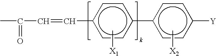
(X1 and X2 are each selected from the group consisting of hydrogen, fluorine, chlorine, CN, NO2, CH3, OCH3, CF3, OCF3; k is 0 to 1; Y is selected from the group consisting of hydrogen, fluorine, chlorine, cyano, NO2, CF3, OCF3, CnH2n+1, OCnH2n+1, CnH2n+1−xFx, OCnH2n+1−xFx (n=1˜10, x=1˜2n+1)).
| TABLE 1 | |||||
| First | Second | Pretilt | |||
| Irradiation | Irradiation | Angle | |||
| Materials | (min) | (sec) | (°) | ||
| Hydroxyethyl Cellulose | 2 | 10 | 4 | ||
| 4-fluorocinnamate | 2 | 20 | 6 | ||
| 2 | 40 | 8 | |||
| Hydroxyethyl Cellulose | 10 | 5 | 3 | ||
| 5-methoxycinnamate | 10 | 10 | 5 | ||
| TABLE 2 | |||||
| Irradiation | Tilt | Thermostability | |||
| Materials | Time (sec) | (°) | (°) | ||
| Polysiloxane | 200 | 0 | 0 | ||
| 4-fluorocinnamate | 1000 | 0 | 0 | ||
| Polyvinyl | 200 | 0 | Alignment | ||
| 4-fluorocinnamate | 500 | 0 | broken | ||
| Hydroxyethyl | 30 | 1 | 1 | ||
| 4-fluorocinnamate | 60 | 2 | 2 | ||
-
- 2-fluoro cinnamic acid;
- 3-fluoro cinnamic acid;
- 3-chloro cinnamic acid;
- 4-chloro cinnamic acid;
- 2-methyl cinnamic acid;
- 4-phenyl cinnamic acid;
- 4-methoxy cinnamic acid;
- 4-pentoxy cinnamic acid;
- 4-heptyloxycinnamic acid;
- 4-nonyloxy cinnamic acid;
- 4-(4-pentoxyphenyl)cinnamic acid;
- 4-trifluoromethoxy cinnamic acid;
- 4-trifluoromethyl cinnamic acid;
- 4-pentyl cinnamic acid; and
- 4-methoxy-3-fluorocinnamic acid.


Claims (8)

Priority Applications (2)
| Application Number | Priority Date | Filing Date | Title |
|---|---|---|---|
| US11/330,156 US7608211B2 (en) | 1999-03-25 | 2006-01-12 | Method of making a liquid crystal display device |
| US12/585,435 US7901605B2 (en) | 1999-03-25 | 2009-09-15 | Method of forming an alignment layer for liquid crystal display device |
Applications Claiming Priority (5)
| Application Number | Priority Date | Filing Date | Title |
|---|---|---|---|
| KR1999-10214 | 1999-03-25 | ||
| KR1019990010214A KR100301853B1 (en) | 1999-03-25 | 1999-03-25 | Alignment layer for liquid crystal display device |
| US09/534,723 US6764724B1 (en) | 1999-03-25 | 2000-03-24 | Alignment layer for a liquid crystal display device |
| US10/846,522 US7014892B2 (en) | 1999-03-25 | 2004-05-17 | Alignment layer for a liquid crystal display device |
| US11/330,156 US7608211B2 (en) | 1999-03-25 | 2006-01-12 | Method of making a liquid crystal display device |
Related Parent Applications (1)
| Application Number | Title | Priority Date | Filing Date |
|---|---|---|---|
| US10/846,522 Continuation US7014892B2 (en) | 1999-03-25 | 2004-05-17 | Alignment layer for a liquid crystal display device |
Related Child Applications (1)
| Application Number | Title | Priority Date | Filing Date |
|---|---|---|---|
| US12/585,435 Division US7901605B2 (en) | 1999-03-25 | 2009-09-15 | Method of forming an alignment layer for liquid crystal display device |
Publications (2)
| Publication Number | Publication Date |
|---|---|
| US20060115607A1 US20060115607A1 (en) | 2006-06-01 |
| US7608211B2 true US7608211B2 (en) | 2009-10-27 |
Family
ID=19577662
Family Applications (4)
| Application Number | Title | Priority Date | Filing Date |
|---|---|---|---|
| US09/534,723 Expired - Lifetime US6764724B1 (en) | 1999-03-25 | 2000-03-24 | Alignment layer for a liquid crystal display device |
| US10/846,522 Expired - Fee Related US7014892B2 (en) | 1999-03-25 | 2004-05-17 | Alignment layer for a liquid crystal display device |
| US11/330,156 Expired - Fee Related US7608211B2 (en) | 1999-03-25 | 2006-01-12 | Method of making a liquid crystal display device |
| US12/585,435 Expired - Fee Related US7901605B2 (en) | 1999-03-25 | 2009-09-15 | Method of forming an alignment layer for liquid crystal display device |
Family Applications Before (2)
| Application Number | Title | Priority Date | Filing Date |
|---|---|---|---|
| US09/534,723 Expired - Lifetime US6764724B1 (en) | 1999-03-25 | 2000-03-24 | Alignment layer for a liquid crystal display device |
| US10/846,522 Expired - Fee Related US7014892B2 (en) | 1999-03-25 | 2004-05-17 | Alignment layer for a liquid crystal display device |
Family Applications After (1)
| Application Number | Title | Priority Date | Filing Date |
|---|---|---|---|
| US12/585,435 Expired - Fee Related US7901605B2 (en) | 1999-03-25 | 2009-09-15 | Method of forming an alignment layer for liquid crystal display device |
Country Status (6)
| Country | Link |
|---|---|
| US (4) | US6764724B1 (en) |
| JP (1) | JP4594484B2 (en) |
| KR (1) | KR100301853B1 (en) |
| DE (1) | DE10015219B9 (en) |
| FR (1) | FR2791440B1 (en) |
| TW (1) | TWI229214B (en) |
Families Citing this family (14)
| Publication number | Priority date | Publication date | Assignee | Title |
|---|---|---|---|---|
| KR100301853B1 (en) * | 1999-03-25 | 2001-09-26 | 구본준, 론 위라하디락사 | Alignment layer for liquid crystal display device |
| KR100375503B1 (en) * | 2000-12-27 | 2003-03-10 | 엘지전선 주식회사 | A photosensitive liquid crystal alignment layer for liquid crystal display element and liquid crystal display using thereit |
| JP4637839B2 (en) | 2003-08-08 | 2011-02-23 | メルク パテント ゲゼルシャフト ミット ベシュレンクテル ハフツング | Alignment layer for aligning liquid crystal molecules with reactive mesogens |
| JP2006317656A (en) * | 2005-05-12 | 2006-11-24 | Dainippon Printing Co Ltd | Anisotropic optical element |
| KR101212135B1 (en) * | 2005-06-14 | 2012-12-14 | 엘지디스플레이 주식회사 | Liquid Crystal Display Device, and method of fabricating the same |
| US7473448B2 (en) * | 2005-12-23 | 2009-01-06 | Eastman Kodak Company | Photoalignment of liquid crystals using poly(vinylstilbazolium) polymers |
| KR20100034874A (en) * | 2008-09-25 | 2010-04-02 | 삼성전자주식회사 | Display having a planarized substrate and method of the same |
| JP5767800B2 (en) * | 2010-11-19 | 2015-08-19 | Jsr株式会社 | Liquid crystal aligning agent and liquid crystal display element |
| JP5825137B2 (en) * | 2011-04-21 | 2015-12-02 | Jsr株式会社 | Liquid crystal aligning agent for retardation film, liquid crystal aligning film for retardation film, retardation film and method for producing the same |
| TWI437332B (en) * | 2011-10-27 | 2014-05-11 | Far Eastern New Century Corp | A method for preparing composite phase difference plate |
| KR101460862B1 (en) * | 2011-11-17 | 2014-11-17 | 주식회사 엘지화학 | Optical elemet |
| CN103135157B (en) * | 2011-11-29 | 2015-02-25 | 远东新世纪股份有限公司 | Method for preparing composite phase difference board |
| KR20150121390A (en) * | 2014-04-18 | 2015-10-29 | 삼성디스플레이 주식회사 | Display device and manufacturing method thereof |
| KR102531454B1 (en) * | 2015-12-30 | 2023-05-10 | 엘지디스플레이 주식회사 | Liquid Crystal Display Device And Method Of Fabricating The Same |
Citations (75)
| Publication number | Priority date | Publication date | Assignee | Title |
|---|---|---|---|---|
| US3912920A (en) | 1974-02-06 | 1975-10-14 | Josuke Kubota | Polarized light illumination device |
| EP0261712A1 (en) | 1986-09-04 | 1988-03-30 | Koninklijke Philips Electronics N.V. | Picture display cell, method of forming an orientation layer on a substrate of the picture display cell and monomeric compounds for use in the orientation layer |
| JPS6460833A (en) | 1987-08-31 | 1989-03-07 | Agency Ind Science Techn | Optical recording element |
| JPH01251344A (en) | 1988-03-30 | 1989-10-06 | Agency Of Ind Science & Technol | Optical recording element |
| JPH01251345A (en) | 1988-03-30 | 1989-10-06 | Agency Of Ind Science & Technol | Optical recording element |
| JPH0255330A (en) | 1988-08-22 | 1990-02-23 | Matsushita Electric Ind Co Ltd | Production of oriented film for liquid crystal |
| US4963448A (en) | 1987-08-31 | 1990-10-16 | Agency Of Industrial Science & Technology | Photorecording element and liquid crystal cell comprising the same |
| US4974941A (en) | 1989-03-08 | 1990-12-04 | Hercules Incorporated | Process of aligning and realigning liquid crystal media |
| JPH02298917A (en) | 1989-05-12 | 1990-12-11 | Agency Of Ind Science & Technol | Optical element |
| JPH0336527A (en) | 1989-07-03 | 1991-02-18 | Agency Of Ind Science & Technol | Optical element |
| JPH03120503A (en) | 1989-10-04 | 1991-05-22 | Matsushita Electric Ind Co Ltd | Polarizing component |
| JPH03241311A (en) | 1990-02-20 | 1991-10-28 | Seiko Epson Corp | Polarization light source device |
| US5073294A (en) | 1990-03-07 | 1991-12-17 | Hercules Incorporated | Process of preparing compositions having multiple oriented mesogens |
| JPH047520A (en) | 1990-04-25 | 1992-01-10 | Agency Of Ind Science & Technol | Method for orienting liquid crystal by linearly polarized light |
| JPH04284421A (en) | 1991-03-13 | 1992-10-09 | Agency Of Ind Science & Technol | Liquid crystal orientation method by diagonal light |
| JPH04350822A (en) | 1991-05-29 | 1992-12-04 | Nec Corp | Liquid crystal oriented film and production thereof and liquid crystal optical element |
| JPH0519208A (en) | 1991-07-10 | 1993-01-29 | Nec Corp | Polarization beam splitter array |
| EP0525473A2 (en) | 1991-07-26 | 1993-02-03 | F. Hoffmann-La Roche Ag | Display device with liquid crystal cell |
| EP0525478A2 (en) | 1991-07-26 | 1993-02-03 | F. Hoffmann-La Roche Ag | Liquid crystal display cell |
| JPH0534699A (en) | 1991-07-29 | 1993-02-12 | Toshiba Corp | Liquid crystal display element |
| JPH0553513A (en) | 1991-08-26 | 1993-03-05 | Toshiba Corp | Production of liquid crystal oriented film |
| EP0549283A2 (en) | 1991-12-20 | 1993-06-30 | Fujitsu Limited | Domain divided liquid crystal display device |
| EP0611786A1 (en) | 1993-02-17 | 1994-08-24 | F. Hoffmann-La Roche Ag | Orientation layer for liquid crystals |
| WO1994028458A1 (en) | 1993-05-28 | 1994-12-08 | Hoechst Aktiengesellschaft | Alignment layer for liquid crystals |
| EP0635748A1 (en) | 1993-07-23 | 1995-01-25 | Sharp Kabushiki Kaisha | Liquid crystal display apparatus and method for producing the same |
| US5389698A (en) | 1991-07-26 | 1995-02-14 | Hoffmann-La Roche Inc. | Process for making photopolymers having varying molecular orientation using light to orient and polymerize |
| JPH0756173A (en) | 1993-08-17 | 1995-03-03 | Stanley Electric Co Ltd | Liquid crystal display element and liquid crystal orientation treatment and production of liquid crystal display element |
| GB2281977A (en) | 1993-09-18 | 1995-03-22 | Gold Star Co | Orientation film for a liquid crystal display |
| WO1995018989A2 (en) | 1994-01-10 | 1995-07-13 | Honeywell Inc. | Method of fabricating multi-domain, liquid crystal displays |
| WO1995022075A1 (en) | 1994-02-09 | 1995-08-17 | The Secretary Of State For Defence | Liquid crystal device alignment |
| US5447662A (en) | 1990-12-21 | 1995-09-05 | Hoffmann-La Roche Inc. | Optically non-linear polymeric coatings |
| US5453862A (en) | 1992-09-04 | 1995-09-26 | Stanley Electric Co., Ltd. | Rubbing-free (chiral) nematic liquid crystal display |
| JPH07261185A (en) | 1994-03-24 | 1995-10-13 | Stanley Electric Co Ltd | Production of liquid crystal display element |
| JPH07318942A (en) | 1994-05-27 | 1995-12-08 | Sharp Corp | Liquid crystal display device, its production and apparatus for production therefor |
| JPH07318861A (en) | 1994-05-19 | 1995-12-08 | Canon Inc | Planar polarizing element, polarization illumination device using the planar polarizing element and projector using the planar polarizing element |
| DE4420585A1 (en) | 1994-06-13 | 1995-12-14 | Merck Patent Gmbh | Electro-optical system |
| US5479282A (en) | 1993-02-10 | 1995-12-26 | Stanley Electric Co., Ltd. | Liquid crystal display of multi-domain structure |
| EP0690334A2 (en) | 1994-06-28 | 1996-01-03 | Hoechst Aktiengesellschaft | Liquid crystal display device |
| EP0708354A1 (en) | 1994-10-14 | 1996-04-24 | International Business Machines Corporation | Liquid crystal display device and method of manufacture |
| US5538823A (en) | 1993-05-20 | 1996-07-23 | Goldstar Co., Ltd. | Liquid crystal device utilizing thermostable polymeric material |
| WO1996022561A1 (en) | 1995-01-20 | 1996-07-25 | Geo-Centers, Inc. | Liquid crystal composition and alignment layer |
| EP0742471A2 (en) | 1995-05-10 | 1996-11-13 | Stanley Electric Co., Ltd. | Arrangement for rubbingless orientation of liquid crystals with tilt |
| US5576862A (en) | 1993-06-29 | 1996-11-19 | Stanley Electric Co., Ltd. | Positive orientations of liquid crystal molecules in a multi-domain liquid crystal display cell |
| JPH08334790A (en) | 1995-06-07 | 1996-12-17 | Fujitsu Ltd | Liquid crystal display panel and its production |
| EP0750212A2 (en) | 1995-06-22 | 1996-12-27 | International Business Machines Corporation | Liquid crystal display device |
| US5602661A (en) | 1993-02-17 | 1997-02-11 | Hoffmann-La Roche Inc. | Optical component |
| GB2309793A (en) | 1996-01-09 | 1997-08-06 | Lg Electronics Inc | Controlling pretilt angle direction in a liquid crystal cell |
| GB2309794A (en) | 1996-02-01 | 1997-08-06 | Lg Electronics Inc | Alignment layers for liquid crystal devices |
| EP0788012A2 (en) | 1996-02-05 | 1997-08-06 | Stanley Electric Co., Ltd. | Homeotropic orientation liquid crystal display and its manufacture |
| GB2310048A (en) | 1995-12-29 | 1997-08-13 | Lg Electronics Inc | Alignment layers for liquid crystal cells |
| JPH09265095A (en) | 1996-03-27 | 1997-10-07 | Matsushita Electric Ind Co Ltd | Production of alignment film for liquid crystal molecule |
| JPH09318946A (en) | 1996-05-27 | 1997-12-12 | Stanley Electric Co Ltd | Production of liquid crystal display element |
| US5705096A (en) | 1995-03-15 | 1998-01-06 | Alps Electric Co., Ltd. | UV crosslinking compound, alignment film for LCD component and LCD component |
| US5712696A (en) | 1994-02-17 | 1998-01-27 | Stanley Electric, Co., Ltd. | Manufacture of LCD device by transferring the orientation state from a parent substrate to a child substrate |
| JPH1073821A (en) | 1996-08-30 | 1998-03-17 | Japan Synthetic Rubber Co Ltd | Production of liquid crystal orienting film |
| GB2317964A (en) | 1996-10-07 | 1998-04-08 | Lg Electronics Inc | Controlling the pretilt of a liquid crystal cell |
| JPH1090684A (en) | 1996-09-12 | 1998-04-10 | Ushio Inc | Oriented film light orienting polarization light irradiating device for liquid crystal display element |
| GB2319093A (en) | 1996-11-07 | 1998-05-13 | Lg Electronics Inc | Fabricating a liquid crystal cell |
| JPH10154658A (en) | 1996-09-27 | 1998-06-09 | Ushio Inc | Proximity aligner with changeable irradiation angle |
| JPH10161126A (en) | 1996-12-03 | 1998-06-19 | Ran Technical Service Kk | Method for forming oriented film and exposing device |
| JPH10195296A (en) | 1996-12-13 | 1998-07-28 | Samsung Display Devices Co Ltd | Light-orientating composition, orientation film comprising the same and liquid crystal display element having the orientation film |
| US5786041A (en) | 1995-06-07 | 1998-07-28 | International Business Machines Corporation | Alignment film, a method for producing the alignment film and a liquid crystal display device using the alignment film |
| US5824377A (en) | 1995-11-20 | 1998-10-20 | Lg Electronics Inc. | Photosensitive material for orientation of liquid crystal device and liquid crystal device thereof |
| JPH10332932A (en) | 1997-05-30 | 1998-12-18 | Ushio Inc | Filter polarizing light in specific wavelength range |
| US5853818A (en) | 1996-07-29 | 1998-12-29 | Lg Electronics, Inc. | Method for manufacturing multi-domain liquid crystal cell |
| US5856430A (en) | 1996-03-29 | 1999-01-05 | Alliant Techsystems Inc. | Process and materials for inducing pre-tilt in liquid crystals and liquid crystal displays |
| WO1999008148A2 (en) | 1997-08-05 | 1999-02-18 | Elsicon, Inc. | Optical exposure systems and processes for alignment of liquid crystals |
| US5880803A (en) | 1995-11-06 | 1999-03-09 | Sharp Kabushiki Kaisha | Liquid crystal display element with a portion of an alignment layer covers spacer is directly bonded to the alignment layer on the other substrate |
| US5882238A (en) | 1995-12-08 | 1999-03-16 | Lg Electronics Inc. | Method for manufacturing bend-aligned liquid crystal cell using light |
| GB2331591A (en) * | 1997-11-21 | 1999-05-26 | Lg Electronics Inc | Alignment layer comprising pyranose or furanose polymer |
| US5909265A (en) | 1996-09-20 | 1999-06-01 | Lg Electronics Inc. | Method of fabricating a multi-domain liquid crystal cell |
| JPH11194344A (en) | 1997-10-29 | 1999-07-21 | Ushio Inc | Polarized light radiation device to orient film for liquid crystal display element |
| JPH11194345A (en) | 1997-10-29 | 1999-07-21 | Ushio Inc | Polarized light radiation device to orient film for liquid crystal display element |
| US5928561A (en) | 1995-09-29 | 1999-07-27 | The Secretary Of State For Defence In Her Britannic Majesty's Government Of The United Kingdom Of Great Britain And Northern Ireland | Polymers for liquid crystal alignment |
| US5982466A (en) | 1996-11-29 | 1999-11-09 | Lg Electronics Inc | Method of forming an alignment layer and a liquid crystal cell having same using patterning by light irradiation |
Family Cites Families (14)
| Publication number | Priority date | Publication date | Assignee | Title |
|---|---|---|---|---|
| JPS5435779B2 (en) * | 1974-06-10 | 1979-11-05 | ||
| JPS6173130A (en) * | 1984-09-19 | 1986-04-15 | Ricoh Co Ltd | Liquid crystal display element |
| JPH0240624A (en) * | 1988-07-29 | 1990-02-09 | Fuji Photo Film Co Ltd | Liquid crystal display element |
| JPH03100520A (en) * | 1989-09-12 | 1991-04-25 | Canon Inc | Ferroelectric liquid crystal element |
| JP3120503B2 (en) | 1991-10-18 | 2000-12-25 | 山陽特殊製鋼株式会社 | Method for producing anisotropic powder |
| DE4226556A1 (en) * | 1992-08-11 | 1994-02-17 | Hoechst Ag | LCD orientation film contg. hexose polymer and macrocyclic modifier - of cryptand, coranand, podand, mercapto and/or ionophore type, esp. for use in ferroelectric LCD, giving good contrast and stability |
| JPH08328005A (en) * | 1995-05-26 | 1996-12-13 | Hitachi Chem Co Ltd | Liquid crystal oriented film, treatment of liquid crystal oriented film, liquid crystal holding substrate, liquid crystal display element, production of liquid crystal display element and material for liquid crystal oriented film |
| US6459463B2 (en) * | 1997-06-14 | 2002-10-01 | L.G. Philips Lcd Co., Ltd. | Reflective liquid crystal display having a bent shape and method of manufacturing thereof |
| KR100255931B1 (en) * | 1997-08-14 | 2000-05-01 | 구본준, 론 위라하디락사 | In-plane switching mode lcd |
| JP3241311B2 (en) | 1997-10-23 | 2001-12-25 | 佐賀工業株式会社 | Concrete pouring device |
| US6335776B1 (en) * | 1998-05-30 | 2002-01-01 | Lg. Philips Lcd Co., Ltd. | Multi-domain liquid crystal display device having an auxiliary electrode formed on the same layer as the pixel electrode |
| JP4350822B2 (en) | 1998-10-27 | 2009-10-21 | 三菱マテリアル株式会社 | Hard film and hard film coated member with excellent wear resistance |
| KR100301853B1 (en) * | 1999-03-25 | 2001-09-26 | 구본준, 론 위라하디락사 | Alignment layer for liquid crystal display device |
| JP4284421B2 (en) | 2001-12-20 | 2009-06-24 | 株式会社大一商会 | Game machine |
-
1999
- 1999-03-25 KR KR1019990010214A patent/KR100301853B1/en not_active IP Right Cessation
-
2000
- 2000-03-24 US US09/534,723 patent/US6764724B1/en not_active Expired - Lifetime
- 2000-03-24 FR FR0003816A patent/FR2791440B1/en not_active Expired - Fee Related
- 2000-03-27 DE DE10015219A patent/DE10015219B9/en not_active Expired - Fee Related
- 2000-03-27 JP JP2000087617A patent/JP4594484B2/en not_active Expired - Fee Related
- 2000-05-03 TW TW089108425A patent/TWI229214B/en not_active IP Right Cessation
-
2004
- 2004-05-17 US US10/846,522 patent/US7014892B2/en not_active Expired - Fee Related
-
2006
- 2006-01-12 US US11/330,156 patent/US7608211B2/en not_active Expired - Fee Related
-
2009
- 2009-09-15 US US12/585,435 patent/US7901605B2/en not_active Expired - Fee Related
Patent Citations (95)
| Publication number | Priority date | Publication date | Assignee | Title |
|---|---|---|---|---|
| US3912920A (en) | 1974-02-06 | 1975-10-14 | Josuke Kubota | Polarized light illumination device |
| EP0261712A1 (en) | 1986-09-04 | 1988-03-30 | Koninklijke Philips Electronics N.V. | Picture display cell, method of forming an orientation layer on a substrate of the picture display cell and monomeric compounds for use in the orientation layer |
| JPS6460833A (en) | 1987-08-31 | 1989-03-07 | Agency Ind Science Techn | Optical recording element |
| US4963448A (en) | 1987-08-31 | 1990-10-16 | Agency Of Industrial Science & Technology | Photorecording element and liquid crystal cell comprising the same |
| JPH01251344A (en) | 1988-03-30 | 1989-10-06 | Agency Of Ind Science & Technol | Optical recording element |
| JPH01251345A (en) | 1988-03-30 | 1989-10-06 | Agency Of Ind Science & Technol | Optical recording element |
| JPH0255330A (en) | 1988-08-22 | 1990-02-23 | Matsushita Electric Ind Co Ltd | Production of oriented film for liquid crystal |
| US5032009A (en) | 1989-03-08 | 1991-07-16 | Hercules Incorporated | Process of aligning and realigning liquid crystal media |
| US4974941A (en) | 1989-03-08 | 1990-12-04 | Hercules Incorporated | Process of aligning and realigning liquid crystal media |
| JPH02298917A (en) | 1989-05-12 | 1990-12-11 | Agency Of Ind Science & Technol | Optical element |
| US5296321A (en) | 1989-07-03 | 1994-03-22 | Agency Of Industrial Science & Technology | Photorecording element, method for production thereof, and the liquid crystal cell comprising the same |
| JPH0336527A (en) | 1989-07-03 | 1991-02-18 | Agency Of Ind Science & Technol | Optical element |
| JPH03120503A (en) | 1989-10-04 | 1991-05-22 | Matsushita Electric Ind Co Ltd | Polarizing component |
| JPH03241311A (en) | 1990-02-20 | 1991-10-28 | Seiko Epson Corp | Polarization light source device |
| US5073294A (en) | 1990-03-07 | 1991-12-17 | Hercules Incorporated | Process of preparing compositions having multiple oriented mesogens |
| JPH047520A (en) | 1990-04-25 | 1992-01-10 | Agency Of Ind Science & Technol | Method for orienting liquid crystal by linearly polarized light |
| US5447662A (en) | 1990-12-21 | 1995-09-05 | Hoffmann-La Roche Inc. | Optically non-linear polymeric coatings |
| JPH04284421A (en) | 1991-03-13 | 1992-10-09 | Agency Of Ind Science & Technol | Liquid crystal orientation method by diagonal light |
| JPH04350822A (en) | 1991-05-29 | 1992-12-04 | Nec Corp | Liquid crystal oriented film and production thereof and liquid crystal optical element |
| JPH0519208A (en) | 1991-07-10 | 1993-01-29 | Nec Corp | Polarization beam splitter array |
| US5784139A (en) | 1991-07-26 | 1998-07-21 | Rolic Ag | Image display device |
| JPH05232473A (en) | 1991-07-26 | 1993-09-10 | F Hoffmann La Roche Ag | Liquid crystal display cell |
| EP0525478A2 (en) | 1991-07-26 | 1993-02-03 | F. Hoffmann-La Roche Ag | Liquid crystal display cell |
| US5389698A (en) | 1991-07-26 | 1995-02-14 | Hoffmann-La Roche Inc. | Process for making photopolymers having varying molecular orientation using light to orient and polymerize |
| EP0525473A2 (en) | 1991-07-26 | 1993-02-03 | F. Hoffmann-La Roche Ag | Display device with liquid crystal cell |
| JPH0534699A (en) | 1991-07-29 | 1993-02-12 | Toshiba Corp | Liquid crystal display element |
| JPH0553513A (en) | 1991-08-26 | 1993-03-05 | Toshiba Corp | Production of liquid crystal oriented film |
| EP0549283A2 (en) | 1991-12-20 | 1993-06-30 | Fujitsu Limited | Domain divided liquid crystal display device |
| US5453862A (en) | 1992-09-04 | 1995-09-26 | Stanley Electric Co., Ltd. | Rubbing-free (chiral) nematic liquid crystal display |
| US5479282A (en) | 1993-02-10 | 1995-12-26 | Stanley Electric Co., Ltd. | Liquid crystal display of multi-domain structure |
| EP0611786A1 (en) | 1993-02-17 | 1994-08-24 | F. Hoffmann-La Roche Ag | Orientation layer for liquid crystals |
| US5602661A (en) | 1993-02-17 | 1997-02-11 | Hoffmann-La Roche Inc. | Optical component |
| US5539074A (en) | 1993-02-17 | 1996-07-23 | Hoffmann-La Roche Inc. | Linear and cyclic polymers or oligomers having a photoreactive ethene group |
| US5538823A (en) | 1993-05-20 | 1996-07-23 | Goldstar Co., Ltd. | Liquid crystal device utilizing thermostable polymeric material |
| WO1994028458A1 (en) | 1993-05-28 | 1994-12-08 | Hoechst Aktiengesellschaft | Alignment layer for liquid crystals |
| US5576862A (en) | 1993-06-29 | 1996-11-19 | Stanley Electric Co., Ltd. | Positive orientations of liquid crystal molecules in a multi-domain liquid crystal display cell |
| EP0635748A1 (en) | 1993-07-23 | 1995-01-25 | Sharp Kabushiki Kaisha | Liquid crystal display apparatus and method for producing the same |
| JPH0756173A (en) | 1993-08-17 | 1995-03-03 | Stanley Electric Co Ltd | Liquid crystal display element and liquid crystal orientation treatment and production of liquid crystal display element |
| US5767994A (en) | 1993-09-18 | 1998-06-16 | Goldstar Co., Ltd. | Orientation film of photopolymer in a liquid crystal display and a method of forming the film |
| US5464669A (en) | 1993-09-18 | 1995-11-07 | Goldstar Co., Ltd. | Method for forming an orientation film of photopolymer in a liquid crystal display |
| GB2281977A (en) | 1993-09-18 | 1995-03-22 | Gold Star Co | Orientation film for a liquid crystal display |
| WO1995018989A2 (en) | 1994-01-10 | 1995-07-13 | Honeywell Inc. | Method of fabricating multi-domain, liquid crystal displays |
| US5657105A (en) | 1994-01-10 | 1997-08-12 | Honeywell Inc. | Multi-domain liquid crystal displays |
| WO1995022075A1 (en) | 1994-02-09 | 1995-08-17 | The Secretary Of State For Defence | Liquid crystal device alignment |
| GB2286893A (en) | 1994-02-09 | 1995-08-30 | Secr Defence | Liquid crystal alignment |
| US5712696A (en) | 1994-02-17 | 1998-01-27 | Stanley Electric, Co., Ltd. | Manufacture of LCD device by transferring the orientation state from a parent substrate to a child substrate |
| JPH07261185A (en) | 1994-03-24 | 1995-10-13 | Stanley Electric Co Ltd | Production of liquid crystal display element |
| JPH07318861A (en) | 1994-05-19 | 1995-12-08 | Canon Inc | Planar polarizing element, polarization illumination device using the planar polarizing element and projector using the planar polarizing element |
| JPH07318942A (en) | 1994-05-27 | 1995-12-08 | Sharp Corp | Liquid crystal display device, its production and apparatus for production therefor |
| US5604615A (en) | 1994-05-27 | 1997-02-18 | Sharp Kabushiki Kaisha | Liquid crystal display device and methods for producing same with alignment layer having new bond formation or bond cleavage reaction of molecular chains by light irradiation |
| WO1995034843A1 (en) | 1994-06-13 | 1995-12-21 | Merck Patent Gmbh | Electro-optical system |
| DE4420585A1 (en) | 1994-06-13 | 1995-12-14 | Merck Patent Gmbh | Electro-optical system |
| EP0690334A2 (en) | 1994-06-28 | 1996-01-03 | Hoechst Aktiengesellschaft | Liquid crystal display device |
| EP0708354A1 (en) | 1994-10-14 | 1996-04-24 | International Business Machines Corporation | Liquid crystal display device and method of manufacture |
| US5764326A (en) | 1994-10-14 | 1998-06-09 | International Business Machines Corporation | Multiple direction rotatable liquid crystal display device and a method for its manufacture |
| US5578351A (en) | 1995-01-20 | 1996-11-26 | Geo-Centers, Inc. | Liquid crystal composition and alignment layer |
| WO1996022561A1 (en) | 1995-01-20 | 1996-07-25 | Geo-Centers, Inc. | Liquid crystal composition and alignment layer |
| US5705096A (en) | 1995-03-15 | 1998-01-06 | Alps Electric Co., Ltd. | UV crosslinking compound, alignment film for LCD component and LCD component |
| EP0742471A2 (en) | 1995-05-10 | 1996-11-13 | Stanley Electric Co., Ltd. | Arrangement for rubbingless orientation of liquid crystals with tilt |
| US5786041A (en) | 1995-06-07 | 1998-07-28 | International Business Machines Corporation | Alignment film, a method for producing the alignment film and a liquid crystal display device using the alignment film |
| JPH08334790A (en) | 1995-06-07 | 1996-12-17 | Fujitsu Ltd | Liquid crystal display panel and its production |
| EP0750212A2 (en) | 1995-06-22 | 1996-12-27 | International Business Machines Corporation | Liquid crystal display device |
| US5928561A (en) | 1995-09-29 | 1999-07-27 | The Secretary Of State For Defence In Her Britannic Majesty's Government Of The United Kingdom Of Great Britain And Northern Ireland | Polymers for liquid crystal alignment |
| US5880803A (en) | 1995-11-06 | 1999-03-09 | Sharp Kabushiki Kaisha | Liquid crystal display element with a portion of an alignment layer covers spacer is directly bonded to the alignment layer on the other substrate |
| US5824377A (en) | 1995-11-20 | 1998-10-20 | Lg Electronics Inc. | Photosensitive material for orientation of liquid crystal device and liquid crystal device thereof |
| US5882238A (en) | 1995-12-08 | 1999-03-16 | Lg Electronics Inc. | Method for manufacturing bend-aligned liquid crystal cell using light |
| GB2310048A (en) | 1995-12-29 | 1997-08-13 | Lg Electronics Inc | Alignment layers for liquid crystal cells |
| US5859682A (en) | 1995-12-29 | 1999-01-12 | Lg Electronics Inc. | Method for manufacturing liquid crystal cell using light |
| GB2309793A (en) | 1996-01-09 | 1997-08-06 | Lg Electronics Inc | Controlling pretilt angle direction in a liquid crystal cell |
| JPH09211465A (en) | 1996-02-01 | 1997-08-15 | Lg Electron Inc | Light irradiating device for light orientation and light irradiating method |
| DE19703682A1 (en) | 1996-02-01 | 1997-08-07 | Lg Electronics Inc | UV light irradiation apparatus for photo alignment processes and irradiation processes using the same |
| US5889571A (en) | 1996-02-01 | 1999-03-30 | Lg Electronics Inc. | Ultraviolet irradiating device for photo-alignment process and an irradiating method using the same |
| GB2309794A (en) | 1996-02-01 | 1997-08-06 | Lg Electronics Inc | Alignment layers for liquid crystal devices |
| JPH09211468A (en) | 1996-02-05 | 1997-08-15 | Stanley Electric Co Ltd | Production of liquid crystal display element and liquid crystal display element |
| EP0788012A2 (en) | 1996-02-05 | 1997-08-06 | Stanley Electric Co., Ltd. | Homeotropic orientation liquid crystal display and its manufacture |
| JPH09265095A (en) | 1996-03-27 | 1997-10-07 | Matsushita Electric Ind Co Ltd | Production of alignment film for liquid crystal molecule |
| US5856430A (en) | 1996-03-29 | 1999-01-05 | Alliant Techsystems Inc. | Process and materials for inducing pre-tilt in liquid crystals and liquid crystal displays |
| US5856431A (en) | 1996-03-29 | 1999-01-05 | Alliant Techsystems Inc. | Process and materials for inducing pre-tilt in liquid crystals and liquid crystal displays |
| JPH09318946A (en) | 1996-05-27 | 1997-12-12 | Stanley Electric Co Ltd | Production of liquid crystal display element |
| US5853818A (en) | 1996-07-29 | 1998-12-29 | Lg Electronics, Inc. | Method for manufacturing multi-domain liquid crystal cell |
| JPH1073821A (en) | 1996-08-30 | 1998-03-17 | Japan Synthetic Rubber Co Ltd | Production of liquid crystal orienting film |
| JPH1090684A (en) | 1996-09-12 | 1998-04-10 | Ushio Inc | Oriented film light orienting polarization light irradiating device for liquid crystal display element |
| US5909265A (en) | 1996-09-20 | 1999-06-01 | Lg Electronics Inc. | Method of fabricating a multi-domain liquid crystal cell |
| JPH10154658A (en) | 1996-09-27 | 1998-06-09 | Ushio Inc | Proximity aligner with changeable irradiation angle |
| GB2317964A (en) | 1996-10-07 | 1998-04-08 | Lg Electronics Inc | Controlling the pretilt of a liquid crystal cell |
| GB2319093A (en) | 1996-11-07 | 1998-05-13 | Lg Electronics Inc | Fabricating a liquid crystal cell |
| US5982466A (en) | 1996-11-29 | 1999-11-09 | Lg Electronics Inc | Method of forming an alignment layer and a liquid crystal cell having same using patterning by light irradiation |
| JPH10161126A (en) | 1996-12-03 | 1998-06-19 | Ran Technical Service Kk | Method for forming oriented film and exposing device |
| JPH10195296A (en) | 1996-12-13 | 1998-07-28 | Samsung Display Devices Co Ltd | Light-orientating composition, orientation film comprising the same and liquid crystal display element having the orientation film |
| JPH10332932A (en) | 1997-05-30 | 1998-12-18 | Ushio Inc | Filter polarizing light in specific wavelength range |
| WO1999008148A2 (en) | 1997-08-05 | 1999-02-18 | Elsicon, Inc. | Optical exposure systems and processes for alignment of liquid crystals |
| JPH11194344A (en) | 1997-10-29 | 1999-07-21 | Ushio Inc | Polarized light radiation device to orient film for liquid crystal display element |
| JPH11194345A (en) | 1997-10-29 | 1999-07-21 | Ushio Inc | Polarized light radiation device to orient film for liquid crystal display element |
| DE19853247A1 (en) | 1997-11-21 | 1999-06-10 | Lg Electronics Inc | Liquid crystal display device |
| GB2331591A (en) * | 1997-11-21 | 1999-05-26 | Lg Electronics Inc | Alignment layer comprising pyranose or furanose polymer |
Non-Patent Citations (35)
| Title |
|---|
| A. Lien, et al., UV modification of surface pretilt of alignment layers of multidomain liquid crystal displays, Appl. Phys. Lett. 62 (21), Nov. 20, 1995, pp. 3108-3111. |
| A. Lien, UV-Type Two-Domain Wide Viewing Angle TFT/LCD Panels, Asia Display '95, pp. 593-596. |
| D. Seo, et al., Invited Address: Surface Alignment of Liquid Crystals in LCDs, SID 93 Digest, pp. 954-956. |
| Eugene Hecht; "Optics"; 1987; pp. 298-299. |
| F. Yamada, et al., Late-News Poster: A New Photo-Alignment Scheme for LC-Cell Pretilt Control, SID 97 Digest, pp. 715-718. |
| H. Soh, et al., The Realization of Wide Viewing Angle TFT-LCDs using Photo-Alignment Method, Euro Display '96, pp. 579-582. |
| J. Chen, Mechanism of Liquid-Crystal Alignment by Polyimide Exposure to Linearly Polarized UV Light, SID 96 Digest, pp. 634-637. |
| J. Chen, Model of liquid crystal alignment by exposure to linearly polarized ultraviolet light, Physical Review E, vol. 54, No. 2, Aug. 1996, pp. 1599-1603. |
| J. Kim, et al., Late-News Poster: Photo-Alignment of Liquid Crystals Using a New Photopolymer, SID 96 Digest, pp. 646-649. |
| J. West, et al., Polarized UV-Exposed Polyimide Films for Liquid-Crystal Alignment, SID 95 Digest, pp. 703-705. |
| Jenkins et al., "Fundamentals of Optics"; McGraw-Hill Book Company; Third Edition; 1957; pp. 492-493. |
| K. Han, et al., A Study on the Photo-Alignment of the Polymer-Containing Cinnamate Group Using a New Single UV-Exposure Method, SID 97 Digest, pp. 707-710. |
| K. Lee, et al., Late-News Poster: Mechanism of UV Modification of LC Pretilt Angle and Its Application to Two-Domain TN-LCDs, SID 96 Digest, pp. 638-641. |
| Kunihiro Ichimura, Photocontrol of Liquid Crystal Alignment, 1993. |
| Lim et al.; "Tilting of Liquid Crystal through Interaction with Methyl Orange Molecules Oriented by Circularly Polarized Light"; JP Journal of Applied Physics; vol. 35; Oct. 1996; pp. 1281-1283. |
| M. Hasegawa, Nematic Homogeneous Photo Alignment by Polyimide Exposure to Linearly Polarized UV, Journal of Photopolymer Science and Technology, vol. 8, No. 2, 1995, pp. 241-248. |
| M. Nam, et al., Wide-Viewing-Angle TFT-LCD with Photo-Aligned Four-Domain TN Mode, SID 97 Digest, pp. 933-936. |
| M. Schadt, et al., Invited Paper: Optical Patterning of Multidomain LCDs, SID 97 Digest, pp. 397-400. |
| M. Schadt, et al., Optical patterning of multi-domain liquid-crystal displays with wide viewing angles, Letters to Nature, vol. 381, May 16, 1996. |
| M. Schadt, et al., Photo-Generation of Linearly Polymerized Liquid Crystal Aligning Layers Comprising Novel, Integrated Optically Patterned Retarders and Color Filters, Jpn. J. Appl. Phys. vol. 34 (1995), pp. 3240-3249, Part 1, No. 6A, Jun. 1995. |
| M. Schadt, Investigation of the Mechanism of the Surface-Induced Alignment of Liquid Crystals by Linearly Polymerized Photopolymers, SID 95 Digest, pp. 528-531. |
| Martin Schadt, Surface-Induced Parallel Alignment of Liquid Crystals by Linearly Polymerized Photopolymers, Jpn. J. Appl. Phys. vol. 31 (1992), Part 1, No. 7, Jul. 1992. |
| P. Shannon, et al., Patterned optical properties in photopolymerized surface-aligned liquid-crystal films, Letters to Nature, vol. 368, Apr. 7, 1994, pp. 532 & 533. |
| R. Shashidhar, et al., A New Non-Rubbing Technique for Liquid-Crystal Alignment, SID 97 Digest, pp. 315-318. |
| T. Hashimoto, et at., TN-LCD with Quartered Subpixels Using Polarized UV-Light-Irradiated Polymer Orientation Films, SID 95 Digest, pp. 877-880. |
| T. Marushii, et al., Photosensitive Orientants for Liquid Crystal Alignment, Mol. Mat. 1993, vol. 3, pp. 161-168. |
| T. Saitoh, et al., A New Hybrid N-TB Mode LCD with Two Domain Pixels Fabricated Using a Photopolymer, Asia Display '95, pp. 589-592. |
| T. Yamamoto, Liquid-Crystal Alignment by Slantwise Irradiation of Non-Polarized UV Light on a Polyimide Layer, SID 96 Digest, pp. 642-645. |
| UK Search Report and Examination, pp. 1-4, Jul. 2000. |
| W. Gibbons, et al., Surface-mediated alignment of nematic liquid crystals with polarized laser light, Letters to Nature, vol. 351, May 2, 1991, pp. 49 & 50. |
| Y. Iimura, et al:, Inveited Address: Electro-Optic Characteristics of Amorphous and Super-Multidomain TN-LCDs Prepared by a Non-Rubbing Method, SID 94 Digest, pp. 915-918. |
| Y. Iimura, Invited Paper: Prospects of the Photo-Alignment Technique for LCD fabrication, SID 97 Digest, pp. 311-314. |
| Y. Saitoh, et al., Stability of UV-Type Two-Domain Wide-Viewing-Angle TFT-LCD Panels, SID 96 Digest, pp. 662-665. |
| Y. Toko, et al., TN-LCDs Fabricated by Non-Rubbing Showing Wide and Homogeneous Viewing Angular Characteristics and Excellent Voltage Holding Ratio, SID 93 Digest, pp. 622-625. |
| Yasufumi Iimura, et al., Alignment Control of a Liquid Crystal on a Photosensitive Polyvinylalcohol Film, Jpn. J. Appln. Phys. vol. 32 (1993), Part 2, No. 1A/B, Jan. 15, 1993. |
Also Published As
| Publication number | Publication date |
|---|---|
| US20100009069A1 (en) | 2010-01-14 |
| JP2001051279A (en) | 2001-02-23 |
| US20040213924A1 (en) | 2004-10-28 |
| DE10015219B4 (en) | 2006-11-23 |
| US6764724B1 (en) | 2004-07-20 |
| DE10015219B9 (en) | 2007-11-15 |
| FR2791440A1 (en) | 2000-09-29 |
| KR20000061276A (en) | 2000-10-16 |
| TWI229214B (en) | 2005-03-11 |
| US20060115607A1 (en) | 2006-06-01 |
| JP4594484B2 (en) | 2010-12-08 |
| KR100301853B1 (en) | 2001-09-26 |
| US7014892B2 (en) | 2006-03-21 |
| US7901605B2 (en) | 2011-03-08 |
| FR2791440B1 (en) | 2006-01-20 |
| DE10015219A1 (en) | 2000-10-12 |
Similar Documents
| Publication | Publication Date | Title |
|---|---|---|
| US7608211B2 (en) | Method of making a liquid crystal display device | |
| US6399165B1 (en) | Liquid crystal display device | |
| US5824377A (en) | Photosensitive material for orientation of liquid crystal device and liquid crystal device thereof | |
| US5538823A (en) | Liquid crystal device utilizing thermostable polymeric material | |
| US6475705B2 (en) | Method for manufacturing a multidomain liquid crystal display panel | |
| US6582784B2 (en) | Liquid crystal display | |
| JP4094764B2 (en) | Liquid crystal alignment agent | |
| KR102250570B1 (en) | Liquid crystal aligning agent, liquid crystal alignment film and liquid crystal display device | |
| US6770335B2 (en) | Photoalignment materials and liquid crystal display device and method for fabricating the same with said materials | |
| EP1281746A2 (en) | Photo-alignment materials for liquid crystal alignment film | |
| US6793987B2 (en) | Photoalignment materials and liquid crystal display fabricated with such photoalignment materials | |
| GB2348294A (en) | Alignment layer for a liquid crystal device | |
| US7060332B2 (en) | Liquid crystal display with alignment film of polyphenylenphthalamide-based material and method for fabricating the same | |
| TWI376554B (en) | Liquid crystal display device | |
| KR100516157B1 (en) | Triazine ring with one more photoactive groups based polyester polymers composition for photoinduced liquid crystal alignment, preparation method of the film for photoinduced liquid crystal thereby and the liguid crystal cell comprising the film | |
| KR100205174B1 (en) | Cinnamate which is photo-polymerization lc orientation material for va mode | |
| Umanskii et al. | P‐103: Photo‐Alignment of Liquid Crystals by Azodyes |
Legal Events
| Date | Code | Title | Description |
|---|---|---|---|
| AS | Assignment |
Owner name: LG.PHILIPS LCD CO., LTD., KOREA, REPUBLIC OF Free format text: ASSIGNMENT OF ASSIGNORS INTEREST;ASSIGNORS:NAM, MI SOOK;CHOI, YOUNG SEOK;REEL/FRAME:017474/0140;SIGNING DATES FROM 20000720 TO 20000724 |
|
| AS | Assignment |
Owner name: LG DISPLAY CO., LTD., KOREA, REPUBLIC OF Free format text: CHANGE OF NAME;ASSIGNOR:LG.PHILIPS LCD CO., LTD.;REEL/FRAME:021754/0230 Effective date: 20080304 Owner name: LG DISPLAY CO., LTD.,KOREA, REPUBLIC OF Free format text: CHANGE OF NAME;ASSIGNOR:LG.PHILIPS LCD CO., LTD.;REEL/FRAME:021754/0230 Effective date: 20080304 |
|
| STCF | Information on status: patent grant |
Free format text: PATENTED CASE |
|
| FEPP | Fee payment procedure |
Free format text: PAYOR NUMBER ASSIGNED (ORIGINAL EVENT CODE: ASPN); ENTITY STATUS OF PATENT OWNER: LARGE ENTITY |
|
| FEPP | Fee payment procedure |
Free format text: PAYOR NUMBER ASSIGNED (ORIGINAL EVENT CODE: ASPN); ENTITY STATUS OF PATENT OWNER: LARGE ENTITY Free format text: PAYER NUMBER DE-ASSIGNED (ORIGINAL EVENT CODE: RMPN); ENTITY STATUS OF PATENT OWNER: LARGE ENTITY |
|
| FPAY | Fee payment |
Year of fee payment: 4 |
|
| FPAY | Fee payment |
Year of fee payment: 8 |
|
| FEPP | Fee payment procedure |
Free format text: MAINTENANCE FEE REMINDER MAILED (ORIGINAL EVENT CODE: REM.); ENTITY STATUS OF PATENT OWNER: LARGE ENTITY |
|
| LAPS | Lapse for failure to pay maintenance fees |
Free format text: PATENT EXPIRED FOR FAILURE TO PAY MAINTENANCE FEES (ORIGINAL EVENT CODE: EXP.); ENTITY STATUS OF PATENT OWNER: LARGE ENTITY |
|
| STCH | Information on status: patent discontinuation |
Free format text: PATENT EXPIRED DUE TO NONPAYMENT OF MAINTENANCE FEES UNDER 37 CFR 1.362 |
|
| FP | Lapsed due to failure to pay maintenance fee |
Effective date: 20211027 |