US7601430B2 - Biaxially oriented film on flexible polymeric substrate - Google Patents
Biaxially oriented film on flexible polymeric substrate Download PDFInfo
- Publication number
- US7601430B2 US7601430B2 US11/345,106 US34510606A US7601430B2 US 7601430 B2 US7601430 B2 US 7601430B2 US 34510606 A US34510606 A US 34510606A US 7601430 B2 US7601430 B2 US 7601430B2
- Authority
- US
- United States
- Prior art keywords
- nitride
- oxide
- flexible template
- template according
- flexible
- Prior art date
- Legal status (The legal status is an assumption and is not a legal conclusion. Google has not performed a legal analysis and makes no representation as to the accuracy of the status listed.)
- Expired - Fee Related, expires
Links
- 239000000758 substrate Substances 0.000 title claims abstract description 60
- 230000006911 nucleation Effects 0.000 claims description 29
- 238000010899 nucleation Methods 0.000 claims description 29
- 239000013078 crystal Substances 0.000 claims description 23
- CPLXHLVBOLITMK-UHFFFAOYSA-N magnesium oxide Inorganic materials [Mg]=O CPLXHLVBOLITMK-UHFFFAOYSA-N 0.000 claims description 23
- 239000000395 magnesium oxide Substances 0.000 claims description 23
- AXZKOIWUVFPNLO-UHFFFAOYSA-N magnesium;oxygen(2-) Chemical compound [O-2].[Mg+2] AXZKOIWUVFPNLO-UHFFFAOYSA-N 0.000 claims description 23
- 150000004767 nitrides Chemical class 0.000 claims description 23
- -1 strontium nitride Chemical class 0.000 claims description 23
- 238000007735 ion beam assisted deposition Methods 0.000 claims description 17
- 229910044991 metal oxide Inorganic materials 0.000 claims description 10
- 150000004706 metal oxides Chemical class 0.000 claims description 10
- UQSXHKLRYXJYBZ-UHFFFAOYSA-N Iron oxide Chemical compound [Fe]=O UQSXHKLRYXJYBZ-UHFFFAOYSA-N 0.000 claims description 8
- 239000004642 Polyimide Substances 0.000 claims description 8
- NRTOMJZYCJJWKI-UHFFFAOYSA-N Titanium nitride Chemical compound [Ti]#N NRTOMJZYCJJWKI-UHFFFAOYSA-N 0.000 claims description 8
- QVQLCTNNEUAWMS-UHFFFAOYSA-N barium oxide Chemical compound [Ba]=O QVQLCTNNEUAWMS-UHFFFAOYSA-N 0.000 claims description 8
- AMWRITDGCCNYAT-UHFFFAOYSA-L hydroxy(oxo)manganese;manganese Chemical compound [Mn].O[Mn]=O.O[Mn]=O AMWRITDGCCNYAT-UHFFFAOYSA-L 0.000 claims description 8
- MRELNEQAGSRDBK-UHFFFAOYSA-N lanthanum(3+);oxygen(2-) Chemical compound [O-2].[O-2].[O-2].[La+3].[La+3] MRELNEQAGSRDBK-UHFFFAOYSA-N 0.000 claims description 8
- PLDDOISOJJCEMH-UHFFFAOYSA-N neodymium(3+);oxygen(2-) Chemical compound [O-2].[O-2].[O-2].[Nd+3].[Nd+3] PLDDOISOJJCEMH-UHFFFAOYSA-N 0.000 claims description 8
- 229920001721 polyimide Polymers 0.000 claims description 8
- IATRAKWUXMZMIY-UHFFFAOYSA-N strontium oxide Chemical compound [O-2].[Sr+2] IATRAKWUXMZMIY-UHFFFAOYSA-N 0.000 claims description 8
- GWEVSGVZZGPLCZ-UHFFFAOYSA-N Titan oxide Chemical compound O=[Ti]=O GWEVSGVZZGPLCZ-UHFFFAOYSA-N 0.000 claims description 4
- WGLPBDUCMAPZCE-UHFFFAOYSA-N Trioxochromium Chemical compound O=[Cr](=O)=O WGLPBDUCMAPZCE-UHFFFAOYSA-N 0.000 claims description 4
- XHCLAFWTIXFWPH-UHFFFAOYSA-N [O-2].[O-2].[O-2].[O-2].[O-2].[V+5].[V+5] Chemical compound [O-2].[O-2].[O-2].[O-2].[O-2].[V+5].[V+5] XHCLAFWTIXFWPH-UHFFFAOYSA-N 0.000 claims description 4
- SJKRCWUQJZIWQB-UHFFFAOYSA-N azane;chromium Chemical compound N.[Cr] SJKRCWUQJZIWQB-UHFFFAOYSA-N 0.000 claims description 4
- BCZWPKDRLPGFFZ-UHFFFAOYSA-N azanylidynecerium Chemical compound [Ce]#N BCZWPKDRLPGFFZ-UHFFFAOYSA-N 0.000 claims description 4
- IBIOTXDDKRNYMC-UHFFFAOYSA-N azanylidynedysprosium Chemical compound [Dy]#N IBIOTXDDKRNYMC-UHFFFAOYSA-N 0.000 claims description 4
- VZVZYLVXLCEAMR-UHFFFAOYSA-N azanylidyneerbium Chemical compound [Er]#N VZVZYLVXLCEAMR-UHFFFAOYSA-N 0.000 claims description 4
- PSBUJOCDKOWAGJ-UHFFFAOYSA-N azanylidyneeuropium Chemical compound [Eu]#N PSBUJOCDKOWAGJ-UHFFFAOYSA-N 0.000 claims description 4
- FLATXDRVRRDFBZ-UHFFFAOYSA-N azanylidynegadolinium Chemical compound [Gd]#N FLATXDRVRRDFBZ-UHFFFAOYSA-N 0.000 claims description 4
- YKIJUSDIPBWHAH-UHFFFAOYSA-N azanylidyneholmium Chemical compound [Ho]#N YKIJUSDIPBWHAH-UHFFFAOYSA-N 0.000 claims description 4
- QCLQZCOGUCNIOC-UHFFFAOYSA-N azanylidynelanthanum Chemical compound [La]#N QCLQZCOGUCNIOC-UHFFFAOYSA-N 0.000 claims description 4
- DPDGELPGCPPHSN-UHFFFAOYSA-N azanylidynelutetium Chemical compound [Lu]#N DPDGELPGCPPHSN-UHFFFAOYSA-N 0.000 claims description 4
- GPBUGPUPKAGMDK-UHFFFAOYSA-N azanylidynemolybdenum Chemical compound [Mo]#N GPBUGPUPKAGMDK-UHFFFAOYSA-N 0.000 claims description 4
- OVMJQLNJCSIJCH-UHFFFAOYSA-N azanylidyneneodymium Chemical compound [Nd]#N OVMJQLNJCSIJCH-UHFFFAOYSA-N 0.000 claims description 4
- CFJRGWXELQQLSA-UHFFFAOYSA-N azanylidyneniobium Chemical compound [Nb]#N CFJRGWXELQQLSA-UHFFFAOYSA-N 0.000 claims description 4
- JCWZBEIBQMTAIH-UHFFFAOYSA-N azanylidynepraseodymium Chemical compound [Pr]#N JCWZBEIBQMTAIH-UHFFFAOYSA-N 0.000 claims description 4
- SZZXSKFKZJTWOY-UHFFFAOYSA-N azanylidynesamarium Chemical compound [Sm]#N SZZXSKFKZJTWOY-UHFFFAOYSA-N 0.000 claims description 4
- CUOITRGULIVMPC-UHFFFAOYSA-N azanylidynescandium Chemical compound [Sc]#N CUOITRGULIVMPC-UHFFFAOYSA-N 0.000 claims description 4
- DOHQPUDBULHKAI-UHFFFAOYSA-N azanylidyneterbium Chemical compound [Tb]#N DOHQPUDBULHKAI-UHFFFAOYSA-N 0.000 claims description 4
- PTXUCVLZGJKEFB-UHFFFAOYSA-N azanylidynethulium Chemical compound [Tm]#N PTXUCVLZGJKEFB-UHFFFAOYSA-N 0.000 claims description 4
- SKKMWRVAJNPLFY-UHFFFAOYSA-N azanylidynevanadium Chemical compound [V]#N SKKMWRVAJNPLFY-UHFFFAOYSA-N 0.000 claims description 4
- XLWMYKCPNRBIDK-UHFFFAOYSA-N azanylidyneytterbium Chemical compound [Yb]#N XLWMYKCPNRBIDK-UHFFFAOYSA-N 0.000 claims description 4
- AJXBBNUQVRZRCZ-UHFFFAOYSA-N azanylidyneyttrium Chemical compound [Y]#N AJXBBNUQVRZRCZ-UHFFFAOYSA-N 0.000 claims description 4
- CXKCTMHTOKXKQT-UHFFFAOYSA-N cadmium oxide Inorganic materials [Cd]=O CXKCTMHTOKXKQT-UHFFFAOYSA-N 0.000 claims description 4
- CFEAAQFZALKQPA-UHFFFAOYSA-N cadmium(2+);oxygen(2-) Chemical compound [O-2].[Cd+2] CFEAAQFZALKQPA-UHFFFAOYSA-N 0.000 claims description 4
- BRPQOXSCLDDYGP-UHFFFAOYSA-N calcium oxide Chemical compound [O-2].[Ca+2] BRPQOXSCLDDYGP-UHFFFAOYSA-N 0.000 claims description 4
- ODINCKMPIJJUCX-UHFFFAOYSA-N calcium oxide Inorganic materials [Ca]=O ODINCKMPIJJUCX-UHFFFAOYSA-N 0.000 claims description 4
- 239000000292 calcium oxide Substances 0.000 claims description 4
- 229910000420 cerium oxide Inorganic materials 0.000 claims description 4
- 229910000423 chromium oxide Inorganic materials 0.000 claims description 4
- 229910000428 cobalt oxide Inorganic materials 0.000 claims description 4
- IVMYJDGYRUAWML-UHFFFAOYSA-N cobalt(ii) oxide Chemical compound [Co]=O IVMYJDGYRUAWML-UHFFFAOYSA-N 0.000 claims description 4
- 229910001940 europium oxide Inorganic materials 0.000 claims description 4
- 229940075616 europium oxide Drugs 0.000 claims description 4
- AEBZCFFCDTZXHP-UHFFFAOYSA-N europium(3+);oxygen(2-) Chemical compound [O-2].[O-2].[O-2].[Eu+3].[Eu+3] AEBZCFFCDTZXHP-UHFFFAOYSA-N 0.000 claims description 4
- 229910052735 hafnium Inorganic materials 0.000 claims description 4
- 229910000480 nickel oxide Inorganic materials 0.000 claims description 4
- 229910000484 niobium oxide Inorganic materials 0.000 claims description 4
- URLJKFSTXLNXLG-UHFFFAOYSA-N niobium(5+);oxygen(2-) Chemical compound [O-2].[O-2].[O-2].[O-2].[O-2].[Nb+5].[Nb+5] URLJKFSTXLNXLG-UHFFFAOYSA-N 0.000 claims description 4
- BMMGVYCKOGBVEV-UHFFFAOYSA-N oxo(oxoceriooxy)cerium Chemical compound [Ce]=O.O=[Ce]=O BMMGVYCKOGBVEV-UHFFFAOYSA-N 0.000 claims description 4
- SIWVEOZUMHYXCS-UHFFFAOYSA-N oxo(oxoyttriooxy)yttrium Chemical group O=[Y]O[Y]=O SIWVEOZUMHYXCS-UHFFFAOYSA-N 0.000 claims description 4
- GNRSAWUEBMWBQH-UHFFFAOYSA-N oxonickel Chemical compound [Ni]=O GNRSAWUEBMWBQH-UHFFFAOYSA-N 0.000 claims description 4
- BPUBBGLMJRNUCC-UHFFFAOYSA-N oxygen(2-);tantalum(5+) Chemical compound [O-2].[O-2].[O-2].[O-2].[O-2].[Ta+5].[Ta+5] BPUBBGLMJRNUCC-UHFFFAOYSA-N 0.000 claims description 4
- UZLYXNNZYFBAQO-UHFFFAOYSA-N oxygen(2-);ytterbium(3+) Chemical compound [O-2].[O-2].[O-2].[Yb+3].[Yb+3] UZLYXNNZYFBAQO-UHFFFAOYSA-N 0.000 claims description 4
- RVTZCBVAJQQJTK-UHFFFAOYSA-N oxygen(2-);zirconium(4+) Chemical compound [O-2].[O-2].[Zr+4] RVTZCBVAJQQJTK-UHFFFAOYSA-N 0.000 claims description 4
- 229910001954 samarium oxide Inorganic materials 0.000 claims description 4
- 229940075630 samarium oxide Drugs 0.000 claims description 4
- FKTOIHSPIPYAPE-UHFFFAOYSA-N samarium(iii) oxide Chemical compound [O-2].[O-2].[O-2].[Sm+3].[Sm+3] FKTOIHSPIPYAPE-UHFFFAOYSA-N 0.000 claims description 4
- HYXGAEYDKFCVMU-UHFFFAOYSA-N scandium oxide Chemical compound O=[Sc]O[Sc]=O HYXGAEYDKFCVMU-UHFFFAOYSA-N 0.000 claims description 4
- 229910052712 strontium Inorganic materials 0.000 claims description 4
- MZLGASXMSKOWSE-UHFFFAOYSA-N tantalum nitride Chemical compound [Ta]#N MZLGASXMSKOWSE-UHFFFAOYSA-N 0.000 claims description 4
- 229910001936 tantalum oxide Inorganic materials 0.000 claims description 4
- OGIDPMRJRNCKJF-UHFFFAOYSA-N titanium oxide Inorganic materials [Ti]=O OGIDPMRJRNCKJF-UHFFFAOYSA-N 0.000 claims description 4
- 229910052721 tungsten Inorganic materials 0.000 claims description 4
- 239000010937 tungsten Substances 0.000 claims description 4
- 229910001935 vanadium oxide Inorganic materials 0.000 claims description 4
- 229910003454 ytterbium oxide Inorganic materials 0.000 claims description 4
- 229940075624 ytterbium oxide Drugs 0.000 claims description 4
- ZVWKZXLXHLZXLS-UHFFFAOYSA-N zirconium nitride Chemical compound [Zr]#N ZVWKZXLXHLZXLS-UHFFFAOYSA-N 0.000 claims description 4
- 229910001928 zirconium oxide Inorganic materials 0.000 claims description 4
- RUDFQVOCFDJEEF-UHFFFAOYSA-N yttrium(III) oxide Inorganic materials [O-2].[O-2].[O-2].[Y+3].[Y+3] RUDFQVOCFDJEEF-UHFFFAOYSA-N 0.000 claims description 2
- 238000000034 method Methods 0.000 abstract description 17
- 229920005570 flexible polymer Polymers 0.000 abstract description 3
- 239000010408 film Substances 0.000 description 16
- 238000000151 deposition Methods 0.000 description 14
- 239000000463 material Substances 0.000 description 11
- 230000008021 deposition Effects 0.000 description 8
- 229920003223 poly(pyromellitimide-1,4-diphenyl ether) Polymers 0.000 description 8
- 229920000642 polymer Polymers 0.000 description 8
- 229920002530 polyetherether ketone Polymers 0.000 description 6
- 239000004696 Poly ether ether ketone Substances 0.000 description 5
- 238000005229 chemical vapour deposition Methods 0.000 description 5
- 238000004519 manufacturing process Methods 0.000 description 5
- 229920002313 fluoropolymer Polymers 0.000 description 4
- 239000004811 fluoropolymer Substances 0.000 description 4
- 229920001778 nylon Polymers 0.000 description 4
- 229920006393 polyether sulfone Polymers 0.000 description 4
- 229920000139 polyethylene terephthalate Polymers 0.000 description 4
- 239000010409 thin film Substances 0.000 description 4
- CSCPPACGZOOCGX-UHFFFAOYSA-N Acetone Chemical compound CC(C)=O CSCPPACGZOOCGX-UHFFFAOYSA-N 0.000 description 3
- OKKJLVBELUTLKV-UHFFFAOYSA-N Methanol Chemical compound OC OKKJLVBELUTLKV-UHFFFAOYSA-N 0.000 description 3
- 239000004952 Polyamide Substances 0.000 description 3
- 239000004743 Polypropylene Substances 0.000 description 3
- FAPWRFPIFSIZLT-UHFFFAOYSA-M Sodium chloride Chemical group [Na+].[Cl-] FAPWRFPIFSIZLT-UHFFFAOYSA-M 0.000 description 3
- 238000005566 electron beam evaporation Methods 0.000 description 3
- 238000005240 physical vapour deposition Methods 0.000 description 3
- 229920003207 poly(ethylene-2,6-naphthalate) Polymers 0.000 description 3
- 229920002647 polyamide Polymers 0.000 description 3
- 229920001155 polypropylene Polymers 0.000 description 3
- 235000002639 sodium chloride Nutrition 0.000 description 3
- 239000011780 sodium chloride Substances 0.000 description 3
- KFZMGEQAYNKOFK-UHFFFAOYSA-N Isopropanol Chemical compound CC(C)O KFZMGEQAYNKOFK-UHFFFAOYSA-N 0.000 description 2
- 229920001646 UPILEX Polymers 0.000 description 2
- 239000000470 constituent Substances 0.000 description 2
- 229910052751 metal Inorganic materials 0.000 description 2
- 239000002184 metal Substances 0.000 description 2
- 230000003287 optical effect Effects 0.000 description 2
- 239000005020 polyethylene terephthalate Substances 0.000 description 2
- 239000004065 semiconductor Substances 0.000 description 2
- 238000004544 sputter deposition Methods 0.000 description 2
- 229910052581 Si3N4 Inorganic materials 0.000 description 1
- 229920006362 Teflon® Polymers 0.000 description 1
- 229910010252 TiO3 Inorganic materials 0.000 description 1
- 238000002441 X-ray diffraction Methods 0.000 description 1
- 229920006102 Zytel® Polymers 0.000 description 1
- 230000006978 adaptation Effects 0.000 description 1
- 230000004888 barrier function Effects 0.000 description 1
- 239000002131 composite material Substances 0.000 description 1
- 239000004020 conductor Substances 0.000 description 1
- 238000005137 deposition process Methods 0.000 description 1
- 238000009792 diffusion process Methods 0.000 description 1
- 230000008020 evaporation Effects 0.000 description 1
- 238000001704 evaporation Methods 0.000 description 1
- 238000010884 ion-beam technique Methods 0.000 description 1
- 150000002500 ions Chemical class 0.000 description 1
- 238000000608 laser ablation Methods 0.000 description 1
- 238000012986 modification Methods 0.000 description 1
- 230000004048 modification Effects 0.000 description 1
- 238000002360 preparation method Methods 0.000 description 1
- 238000005546 reactive sputtering Methods 0.000 description 1
- 238000003980 solgel method Methods 0.000 description 1
Images


Classifications
-
- B—PERFORMING OPERATIONS; TRANSPORTING
- B32—LAYERED PRODUCTS
- B32B—LAYERED PRODUCTS, i.e. PRODUCTS BUILT-UP OF STRATA OF FLAT OR NON-FLAT, e.g. CELLULAR OR HONEYCOMB, FORM
- B32B27/00—Layered products comprising a layer of synthetic resin
-
- H—ELECTRICITY
- H01—ELECTRIC ELEMENTS
- H01L—SEMICONDUCTOR DEVICES NOT COVERED BY CLASS H10
- H01L31/00—Semiconductor devices sensitive to infrared radiation, light, electromagnetic radiation of shorter wavelength or corpuscular radiation and specially adapted either for the conversion of the energy of such radiation into electrical energy or for the control of electrical energy by such radiation; Processes or apparatus specially adapted for the manufacture or treatment thereof or of parts thereof; Details thereof
- H01L31/0248—Semiconductor devices sensitive to infrared radiation, light, electromagnetic radiation of shorter wavelength or corpuscular radiation and specially adapted either for the conversion of the energy of such radiation into electrical energy or for the control of electrical energy by such radiation; Processes or apparatus specially adapted for the manufacture or treatment thereof or of parts thereof; Details thereof characterised by their semiconductor bodies
- H01L31/036—Semiconductor devices sensitive to infrared radiation, light, electromagnetic radiation of shorter wavelength or corpuscular radiation and specially adapted either for the conversion of the energy of such radiation into electrical energy or for the control of electrical energy by such radiation; Processes or apparatus specially adapted for the manufacture or treatment thereof or of parts thereof; Details thereof characterised by their semiconductor bodies characterised by their crystalline structure or particular orientation of the crystalline planes
- H01L31/0392—Semiconductor devices sensitive to infrared radiation, light, electromagnetic radiation of shorter wavelength or corpuscular radiation and specially adapted either for the conversion of the energy of such radiation into electrical energy or for the control of electrical energy by such radiation; Processes or apparatus specially adapted for the manufacture or treatment thereof or of parts thereof; Details thereof characterised by their semiconductor bodies characterised by their crystalline structure or particular orientation of the crystalline planes including thin films deposited on metallic or insulating substrates ; characterised by specific substrate materials or substrate features or by the presence of intermediate layers, e.g. barrier layers, on the substrate
- H01L31/03926—Semiconductor devices sensitive to infrared radiation, light, electromagnetic radiation of shorter wavelength or corpuscular radiation and specially adapted either for the conversion of the energy of such radiation into electrical energy or for the control of electrical energy by such radiation; Processes or apparatus specially adapted for the manufacture or treatment thereof or of parts thereof; Details thereof characterised by their semiconductor bodies characterised by their crystalline structure or particular orientation of the crystalline planes including thin films deposited on metallic or insulating substrates ; characterised by specific substrate materials or substrate features or by the presence of intermediate layers, e.g. barrier layers, on the substrate comprising a flexible substrate
-
- Y—GENERAL TAGGING OF NEW TECHNOLOGICAL DEVELOPMENTS; GENERAL TAGGING OF CROSS-SECTIONAL TECHNOLOGIES SPANNING OVER SEVERAL SECTIONS OF THE IPC; TECHNICAL SUBJECTS COVERED BY FORMER USPC CROSS-REFERENCE ART COLLECTIONS [XRACs] AND DIGESTS
- Y02—TECHNOLOGIES OR APPLICATIONS FOR MITIGATION OR ADAPTATION AGAINST CLIMATE CHANGE
- Y02E—REDUCTION OF GREENHOUSE GAS [GHG] EMISSIONS, RELATED TO ENERGY GENERATION, TRANSMISSION OR DISTRIBUTION
- Y02E10/00—Energy generation through renewable energy sources
- Y02E10/50—Photovoltaic [PV] energy
-
- Y—GENERAL TAGGING OF NEW TECHNOLOGICAL DEVELOPMENTS; GENERAL TAGGING OF CROSS-SECTIONAL TECHNOLOGIES SPANNING OVER SEVERAL SECTIONS OF THE IPC; TECHNICAL SUBJECTS COVERED BY FORMER USPC CROSS-REFERENCE ART COLLECTIONS [XRACs] AND DIGESTS
- Y10—TECHNICAL SUBJECTS COVERED BY FORMER USPC
- Y10T—TECHNICAL SUBJECTS COVERED BY FORMER US CLASSIFICATION
- Y10T428/00—Stock material or miscellaneous articles
- Y10T428/26—Web or sheet containing structurally defined element or component, the element or component having a specified physical dimension
- Y10T428/269—Web or sheet containing structurally defined element or component, the element or component having a specified physical dimension including synthetic resin or polymer layer or component
-
- Y—GENERAL TAGGING OF NEW TECHNOLOGICAL DEVELOPMENTS; GENERAL TAGGING OF CROSS-SECTIONAL TECHNOLOGIES SPANNING OVER SEVERAL SECTIONS OF THE IPC; TECHNICAL SUBJECTS COVERED BY FORMER USPC CROSS-REFERENCE ART COLLECTIONS [XRACs] AND DIGESTS
- Y10—TECHNICAL SUBJECTS COVERED BY FORMER USPC
- Y10T—TECHNICAL SUBJECTS COVERED BY FORMER US CLASSIFICATION
- Y10T428/00—Stock material or miscellaneous articles
- Y10T428/31504—Composite [nonstructural laminate]
- Y10T428/31721—Of polyimide
Definitions
- the invention relates to templates for films used in electronic device applications such as photovoltaic cells, light emitting diodes, and the like. More particularly, the invention relates to flexible templates for such films.
- Polymer-based substrates are of particular interest for use in applications such as flexible electronics, sensors, solar cells, and displays.
- devices that use such polymer-based substrates suffer from poor performance due to the fact that the oxide, nitride, or semiconductor films deposited on the substrate are either amorphous or polycrystalline.
- the present invention meets these and other needs by providing a flexible polymer-based substrate having a biaxially oriented film grown on the surface of the polymer. Methods of forming such a substrate and providing the polymeric substrate with a biaxially oriented film are also described.
- the template having the biaxially oriented film can be used for further epitaxial growth of films of interest for applications such as photovoltaic cells, light emitting diodes, and the like.
- one aspect of the invention is to provide a flexible template for a device.
- the flexible template comprises: a flexible polymeric substrate; a biaxially oriented intermediate layer disposed over the flexible polymeric substrate; and a biaxially oriented buffer layer epitaxially grown on the intermediate layer.
- a second aspect of the invention is to provide a flexible template.
- the flexible template comprises: a flexible polymeric substrate, wherein the flexible polymeric substrate comprises a polymer selected from the group consisting of polyimides, polyetheretherketones, polyethersulfones, nylons, fluoropolymers, polyamides, polyethylene terephthalates, polyethylene naphthalates, polypropylene, and combinations thereof; a biaxially oriented intermediate layer disposed over the flexible polymeric substrate, wherein the intermediate layer is deposited by ion beam assisted deposition and has a face-centered cubic-based structure, and wherein the intermediate layer is one of a nitride and an oxide; and a biaxially oriented buffer layer epitaxially grown on the intermediate layer.
- a third aspect of the invention is to provide a flexible template.
- the flexible template comprises: a flexible polymeric substrate, wherein the flexible polymeric substrate comprises a polymer selected from the group consisting of polyimides, polyetheretherketones, polyethersulfones, nylons, fluoropolymers, polyamides, polyethylene terephthalates, polyethylene naphthalates, polypropylene, and combinations thereof; a nucleation layer disposed on a surface of the polyimide base; a biaxially oriented intermediate layer disposed on the nucleation layer, wherein the intermediate layer is deposited by ion beam assisted deposition and has a face-centered cubic-based crystal structure, and wherein the intermediate layer is one of a nitride and an oxide; and a biaxially oriented buffer layer epitaxially grown on the intermediate layer.
- a fourth aspect of the invention is to provide a method of making a flexible template, wherein the substrate comprises a flexible polymeric substrate, a biaxially oriented intermediate layer disposed over the flexible polymeric substrate, and a biaxially oriented buffer layer epitaxially grown on the intermediate layer.
- the method comprises the steps of: providing the flexible polymeric substrate; depositing the biaxially oriented intermediate layer over the flexible polymeric substrate by ion beam assisted deposition; and epitaxially depositing the biaxially oriented buffer layer on the biaxially oriented intermediate layer to form the flexible template.
- a fifth aspect of the invention is to provide a method of providing a biaxially oriented crystal surface to a flexible polymeric substrate.
- the method comprises the steps of: providing the flexible polymeric substrate; depositing a biaxially oriented intermediate layer over the flexible polymeric substrate by ion beam assisted deposition; and depositing a biaxially oriented buffer layer on the biaxially oriented intermediate layer to form the flexible template.
- FIG. 1 is a schematic representation of a flexible template
- FIG. 2 is a schematic representation of a second template
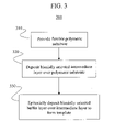
- FIG. 3 is a flow chart for a method of making a flexible template
- FIG. 4 is a flow chart for a method of providing a biaxially oriented crystal surface to a flexible polymeric substrate.
- Flexible template 100 permits the subsequent growth of epitaxial layers thereupon.
- Flexible template 100 includes a flexible polymeric substrate 110 , a biaxially oriented intermediate layer 120 disposed over flexible polymeric substrate 110 , and a biaxially oriented buffer layer 130 epitaxially deposited on intermediate layer biaxially oriented intermediate layer 120 .
- a second embodiment shown in FIG.
- substrate 200 comprises flexible polymeric substrate 110 , biaxially oriented intermediate layer 120 , and biaxially oriented buffer layer 130 as described above, and further includes a nucleation layer 140 disposed between flexible polymeric substrate 110 and biaxially oriented intermediate layer 120 .
- flexible polymeric substrate 110 serves as a flexible base upon which subsequent layers may be deposited.
- flexible polymeric substrate 110 comprises a polyimide such as, for example, Kapton® or Upilex®.
- flexible polymeric substrate 110 may comprise other polymeric materials such as, but not limited to, polyetheretherketones (PEEK), such as Ketron®; polyethersulfones, such as Supradel®; nylons, such as Zytel®; fluoropolymers, such as Teflon®; polyimide/fluoropolymer composites, such as Oasis®; polyamides; polyethylene terephthalate (PET); polyethylene naphthalates, such as Kaladex®; polypropylene films; and the like.
- PEEK polyetheretherketones
- Ketron® such as Ketron®
- polyethersulfones such as Supradel®
- nylons such as Zytel®
- fluoropolymers such as Teflon®
- Polyetheretherketones are stable up to about 300° C.
- polyethersulfones and nylons are stable up to temperatures in a range from about 250° C. to about 265° C.
- Flexible polymeric substrate 110 has a thickness in a range from about 5 microns to about 500 microns.
- an “epitaxial” or “epitaxially deposited” layer is a layer in which the biaxial orientation or crystallographic texture of the underlying “host” material (e.g., a template or buffer layer) onto which the layer is grown defines a corresponding biaxial orientation or crystallographic texture in the layer.
- the underlying material and the epitaxially deposited layer need not have the same crystal structure.
- the terms “biaxially oriented” and “biaxial orientation” refer to a surface or layer in which the crystal grains are in close alignment both in the plane and out of the plane (i.e., perpendicular to the plane) of the surface of the layer.
- One type of biaxially oriented surface is a cubic textured surface in which the crystal grains are in close alignment with directions both parallel and perpendicular to the surface.
- Biaxially oriented intermediate layer 120 establishes a crystallographic template upon which successive layers of material having the same or similar crystallographic orientation or texture may be deposited.
- biaxially oriented intermediate layer 120 comprises at least one of an oxide and a nitride.
- the oxide has a face-centered cubic-based crystal structure (such as, for example, a rock salt structure) and may be a binary metal oxide.
- Non-limiting examples of such binary metal oxides include magnesium oxide, calcium oxide, strontium oxide, barium oxide, titanium oxide, zirconium oxide, vanadium oxide, niobium oxide, tantalum oxide, chromium oxide, manganese oxide, iron oxide, cobalt oxide, nickel oxide, cadmium oxide, scandium oxide, lanthanum oxide, cerium oxide, neodymium oxide, samarium oxide, europium oxide, ytterbium oxide, combinations thereof, and the like.
- the biaxially oriented intermediate layer comprises magnesium oxide.
- the nitride also has a face-centered cubic-based crystal structure, and may be one of strontium nitride, scandium nitride, yttrium nitride, titanium nitride, zirconium nitride, hafnium nitride, vanadium nitride, niobium nitride, tantalum nitride, chromium nitride, molybdenum nitride, tungsten nitride, lanthanum nitride, cerium nitride, praseodymium nitride, neodymium nitride, samarium nitride, europium nitride, gadolinium nitride, terbium nitride, dysprosium nitride, holmium nitride, erbium nitride, ytter
- biaxially oriented intermediate layer 120 comprises an oxide as described hereinabove, and is deposited on either flexible polymeric substrate 110 or nucleation layer 140 using ion beam assisted deposition (also referred to herein as “IBAD”), which also includes reactive ion beam assisted deposition (also referred to herein as “RIBAD”).
- IBAD is a low temperature deposition process that has been widely used in the preparation of templates for high temperature superconducting films in coated conductors.
- IBAD texturing can produce nearly single-crystalline films with crystallographic properties approaching those of conventional epitaxial thin films by using an off-normal ion beam to establish a preferred orientation for film growth on a non-single-crystalline (i.e., amorphous or polycrystalline) substrate.
- the IBAD layer serves as a biaxially oriented template for the epitaxial growth of subsequent layers.
- the principles of IBAD are described in U.S. Pat. No. 5,650,378 by Yauhiro Iijima et al., entitled “Method of making Polycrystalline Thin Film and Superconducting Body,” and issued on Jul. 22, 1997, and U.S. Pat. No. 5,872,080 by Paul N. Arendt et al., entitled “High Temperature Superconducting Thick Films, issued Feb. 16, 1999.
- the contents of U.S. Pat. Nos. 5,650,378 and 5,872,080 are incorporated herein by reference in their entirety.
- biaxially oriented intermediate layer 120 comprises a nitride as described hereinabove, and is deposited on either flexible polymeric substrate 110 or nucleation layer 140 using IBAD or RIBAD.
- the nitride is formed by providing the metal constituent of the nitride to either flexible polymeric substrate 110 or nucleation layer 140 .
- the metal constituent may provided by either physical vapor deposition or chemical vapor deposition, while directing a beam comprising Ar + and N + ions at either flexible polymeric substrate 110 or nucleation layer 140 at a predetermined angle (usually about 45°) from an axis normal to either flexible polymeric substrate 110 or nucleation layer 140 .
- Biaxially oriented buffer layer 130 is epitaxially deposited on intermediate layer 120 and is biaxially oriented with respect to intermediate layer 120 .
- Biaxially oriented buffer layer 130 extends the crystalline order established by intermediate layer 120 and serves to achieve a desired combined thickness of biaxially oriented intermediate layer 120 and buffer layer 130 .
- biaxially oriented buffer layer 130 provides a diffusion barrier between flexible polymeric substrate 110 and any additional layers that may be deposited over buffer layer 130 .
- biaxially oriented buffer layer 130 comprises at least one of an oxide and a nitride having a cubic-based crystal structure (for example, a simple cubic, face-centered cubic, body-centered cubic, or rock salt structure).
- the oxide or nitride has a rock salt crystal structure.
- the oxide may be a binary oxide such as, but not limited to, magnesium oxide, calcium oxide, strontium oxide, barium oxide, titanium oxide, zirconium oxide, vanadium oxide, niobium oxide, tantalum oxide, chromium oxide, manganese oxide, iron oxide, cobalt oxide, nickel oxide, cadmium oxide, scandium oxide, lanthanum oxide, cerium oxide, neodymium oxide, samarium oxide, europium oxide, ytterbium oxide, and combinations thereof.
- the biaxially oriented intermediate layer comprises magnesium oxide.
- the nitride also has a cubic-based crystal structure, and may be one of strontium nitride, scandium nitride, yttrium nitride, titanium nitride, zirconium nitride, hafnium nitride, vanadium nitride, niobium nitride, tantalum nitride, chromium nitride, molybdenum nitride, tungsten nitride, lanthanum nitride, cerium nitride, praseodymium nitride, neodymium nitride, samarium nitride, europium nitride, gadolinium nitride, terbium nitride, dysprosium nitride, holmium nitride, erbium nitride, ytterbium
- the nitride is titanium nitride.
- Biaxially oriented buffer layer 130 has a thickness in a range from about 50 nm to about 500 nm.
- Biaxially oriented buffer layer 130 may be formed by various deposition methods known in the art, such as sputtering (including reactive sputtering), electron beam evaporation, metal-organic deposition, metal-organic chemical vapor deposition, chemical vapor deposition, polymer assisted deposition, laser ablation, and the like.
- Biaxially oriented intermediate layer 120 and buffer layer 130 may comprise the same material, in which case buffer layer 130 is homoepitaxially deposited on intermediate layer 120 .
- both layers comprise magnesium oxide (MgO).
- biaxially oriented intermediate layer 120 and buffer layer 130 may comprise different materials.
- a nucleation layer 140 is disposed on flexible polymeric substrate 110 such that nucleation layer 140 is disposed between flexible polymeric substrate 110 and biaxially oriented intermediate layer 120 .
- Nucleation layer 140 enables texturing of the IBAD-deposited biaxially oriented intermediate layer 120 .
- Nucleation layer 140 comprises, in one embodiment, an oxide such as, but not limited to, yttrium oxide (Y 2 O 3 ) or the like.
- nucleation layer 140 may comprise a nitride.
- amorphous Si 3 N 4 has been used as a nucleation layer for IBAD-deposited MgO.
- Nucleation layer 140 may be deposited by electronic beam (e-beam) evaporation, and has a thickness in a range from about 1 nm to about 20 nm.
- e-beam electronic beam
- Other methods known in the art, such as sol-gel methods, chemical vapor deposition (CVD), sputtering and other physical vapor deposition (PVD) methods, and the like may be used as well.
- biaxially oriented buffer layer 130 may be used directly.
- at least one active layer may be deposited on or over biaxially oriented buffer layer 130 to adapt flexible template 100 to selected applications.
- additional epitaxial films such as ferroelectrics (e.g., Sr 1-x Ba x TiO 3 ) are needed for memory or other electronics applications, such films may be grown hetero-epitaxially on or over biaxially oriented buffer layer 130 using low temperature processes such as sol-gel techniques and the like.
- Flexible template 100 may also be used in other applications such as, but not limited to, sensors, photovoltaic cells, light emitting diodes (LEDs), and transistors, that include at least one semiconducting active layer.
- semiconducting active layers must be deposited at sufficiently low temperatures. Subsequent layers on Kapton® and Upilex®, for example, should be deposited at temperature of less than about 450° C. For other materials, even lower deposition temperatures should be used.
- a method of making flexible templates 100 , 200 described herein is also provided.
- a flow chart for method 300 is shown in FIG. 3 .
- the materials and methods of depositing individual layers that comprise flexible templates 100 , 200 have been previously described herein.
- Step 310 a flexible polymeric substrate 110 is provided.
- step 320 a biaxially oriented intermediate layer 120 is then deposited over flexible polymeric substrate 110 .
- nucleation layer 140 is deposited on flexible polymeric substrate 110 prior to deposition of intermediate layer 120 .
- a biaxially oriented buffer layer 130 is epitaxially deposited on intermediate layer 120 to form flexible template 100 , 200 .
- the invention also provides a method of providing a biaxially oriented crystal surface to a flexible polymeric substrate.
- a flow chart for method 400 is shown in FIG. 4 .
- Step 410 a flexible polymeric substrate 110 is first provided.
- a biaxially oriented intermediate layer 120 is then deposited over flexible polymeric substrate 110 by ion beam assisted deposition (Step 420 ).
- Biaxially oriented buffer layer 130 is then epitaxially deposited on intermediate layer 120 to from the biaxially oriented crystal surface (Step 430 ).
- nucleation layer 140 is deposited on flexible polymeric substrate 110 prior to deposition of intermediate layer 120 .
- MgO biaxially oriented magnesium oxide
- Kapton® tape having a thickness of 2 mil was provided and cleaned with acetone, methanol, and isopropanol.
- a nucleation layer of yttria (Y 2 O 3 ) was deposited on the Kapton® tape at room temperature (i.e., the Kapton® tape was not actively heated, nor did the temperature of the Kapton® tape substantially exceed room temperature) using electron beam evaporation.
- the nucleation layer was deposited at a rate of 0.15 nm/s and had a thickness of about 9 nm.
- a 10 nm thick MgO was then deposited at room temperature using IBAD to achieve biaxial texture. During MgO deposition, the substrate was not actively heated and did not substantially exceed room temperature.
- an Ar + beam (40 mA/750 V with Ar gas flow of 10 sccm) was directed at the nucleation layer/Kapton® tape substrate at 45° to normal.
- the IBAD MgO deposition took place at a rate of about 0.2 nm/s.
- An MgO buffer layer having thicknesses in a range from about 50 nm to about 100 nm was then homoepitaxially deposited on the MgO intermediate layer using electron-beam evaporation.
- the MgO buffer layer was deposited at a rate of 0.1 nm/s and at about 300° C. under a pressure of about 5 ⁇ 10 ⁇ 5 Torr of O 2 .
Abstract
Description
Claims (24)
Priority Applications (2)
| Application Number | Priority Date | Filing Date | Title |
|---|---|---|---|
| US11/345,106 US7601430B2 (en) | 2006-01-31 | 2006-01-31 | Biaxially oriented film on flexible polymeric substrate |
| PCT/US2007/002724 WO2007089886A2 (en) | 2006-01-31 | 2007-01-31 | Biaxially oriented film on flexible polymeric substrate |
Applications Claiming Priority (1)
| Application Number | Priority Date | Filing Date | Title |
|---|---|---|---|
| US11/345,106 US7601430B2 (en) | 2006-01-31 | 2006-01-31 | Biaxially oriented film on flexible polymeric substrate |
Publications (2)
| Publication Number | Publication Date |
|---|---|
| US20090214859A1 US20090214859A1 (en) | 2009-08-27 |
| US7601430B2 true US7601430B2 (en) | 2009-10-13 |
Family
ID=38328049
Family Applications (1)
| Application Number | Title | Priority Date | Filing Date |
|---|---|---|---|
| US11/345,106 Expired - Fee Related US7601430B2 (en) | 2006-01-31 | 2006-01-31 | Biaxially oriented film on flexible polymeric substrate |
Country Status (2)
| Country | Link |
|---|---|
| US (1) | US7601430B2 (en) |
| WO (1) | WO2007089886A2 (en) |
Cited By (5)
| Publication number | Priority date | Publication date | Assignee | Title |
|---|---|---|---|---|
| US20090114274A1 (en) * | 2007-11-02 | 2009-05-07 | Fritzemeier Leslie G | Crystalline thin-film photovoltaic structures |
| US20100270653A1 (en) * | 2009-04-24 | 2010-10-28 | Christopher Leitz | Crystalline thin-film photovoltaic structures and methods for forming the same |
| US20110027937A1 (en) * | 2005-08-25 | 2011-02-03 | Fritzemeier Leslie G | Methods of forming photovoltaic devices |
| US8236603B1 (en) | 2008-09-04 | 2012-08-07 | Solexant Corp. | Polycrystalline semiconductor layers and methods for forming the same |
| US8415187B2 (en) | 2009-01-28 | 2013-04-09 | Solexant Corporation | Large-grain crystalline thin-film structures and devices and methods for forming the same |
Families Citing this family (4)
| Publication number | Priority date | Publication date | Assignee | Title |
|---|---|---|---|---|
| US20080272421A1 (en) * | 2007-05-02 | 2008-11-06 | Micron Technology, Inc. | Methods, constructions, and devices including tantalum oxide layers |
| WO2009155122A2 (en) | 2008-05-30 | 2009-12-23 | Alta Devices, Inc. | Epitaxial lift off stacks and methods |
| US8878189B2 (en) * | 2009-03-27 | 2014-11-04 | Dowa Holdings Co., Ltd. | Group III nitride semiconductor growth substrate, group III nitride semiconductor epitaxial substrate, group III nitride semiconductor element and group III nitride semiconductor free-standing substrate, and method of producing the same |
| US9312436B2 (en) * | 2011-05-16 | 2016-04-12 | Kabushiki Kaisha Toshiba | Nitride semiconductor device, nitride semiconductor wafer, and method for manufacturing nitride semiconductor layer |
Citations (13)
| Publication number | Priority date | Publication date | Assignee | Title |
|---|---|---|---|---|
| EP0631297A2 (en) * | 1993-06-24 | 1994-12-28 | AT&T Corp. | Method for low temperature growth of epitaxial silicon and devices produced thereby |
| US5432151A (en) * | 1993-07-12 | 1995-07-11 | Regents Of The University Of California | Process for ion-assisted laser deposition of biaxially textured layer on substrate |
| US5449659A (en) * | 1991-07-05 | 1995-09-12 | Conductus, Inc. | Method of bonding multilayer structures of crystalline materials |
| US5650378A (en) | 1992-10-02 | 1997-07-22 | Fujikura Ltd. | Method of making polycrystalline thin film and superconducting oxide body |
| US5772755A (en) * | 1996-08-01 | 1998-06-30 | W. L. Gore & Associates, Inc. | Oriented crystalline materials |
| US5872080A (en) | 1995-04-19 | 1999-02-16 | The Regents Of The University Of California | High temperature superconducting thick films |
| WO2001070005A2 (en) * | 2000-03-22 | 2001-09-27 | The Regents Of The University Of California | Method of forming a low temperature metal bond for use in the transfer of bulk and thin film materials |
| US20020073918A1 (en) * | 2000-12-15 | 2002-06-20 | Reade Ronald P. | Particle beam biaxial orientation of a substrate for epitaxial crystal growth |
| US20030036483A1 (en) * | 2000-12-06 | 2003-02-20 | Arendt Paul N. | High temperature superconducting thick films |
| US6872988B1 (en) * | 2004-03-23 | 2005-03-29 | Ut-Battelle, Llc | Semiconductor films on flexible iridium substrates |
| US20060099778A1 (en) * | 2004-11-08 | 2006-05-11 | Samsung Electronics Co., Ltd. | Method of preparing semiconductor film on a substrate |
| US20060208257A1 (en) * | 2005-03-15 | 2006-09-21 | Branz Howard M | Method for low-temperature, hetero-epitaxial growth of thin film cSi on amorphous and multi-crystalline substrates and c-Si devices on amorphous, multi-crystalline, and crystalline substrates |
| US20070114124A1 (en) * | 2005-11-21 | 2007-05-24 | The Regents Of The University Of California | Charge-free low-temperature method of forming thin film-based nanoscale materials and structures on a substrate |
-
2006
- 2006-01-31 US US11/345,106 patent/US7601430B2/en not_active Expired - Fee Related
-
2007
- 2007-01-31 WO PCT/US2007/002724 patent/WO2007089886A2/en active Application Filing
Patent Citations (15)
| Publication number | Priority date | Publication date | Assignee | Title |
|---|---|---|---|---|
| US5449659A (en) * | 1991-07-05 | 1995-09-12 | Conductus, Inc. | Method of bonding multilayer structures of crystalline materials |
| US5650378A (en) | 1992-10-02 | 1997-07-22 | Fujikura Ltd. | Method of making polycrystalline thin film and superconducting oxide body |
| EP0631297A2 (en) * | 1993-06-24 | 1994-12-28 | AT&T Corp. | Method for low temperature growth of epitaxial silicon and devices produced thereby |
| US5523587A (en) * | 1993-06-24 | 1996-06-04 | At&T Corp. | Method for low temperature growth of epitaxial silicon and devices produced thereby |
| US5432151A (en) * | 1993-07-12 | 1995-07-11 | Regents Of The University Of California | Process for ion-assisted laser deposition of biaxially textured layer on substrate |
| US5872080A (en) | 1995-04-19 | 1999-02-16 | The Regents Of The University Of California | High temperature superconducting thick films |
| US5772755A (en) * | 1996-08-01 | 1998-06-30 | W. L. Gore & Associates, Inc. | Oriented crystalline materials |
| WO2001070005A2 (en) * | 2000-03-22 | 2001-09-27 | The Regents Of The University Of California | Method of forming a low temperature metal bond for use in the transfer of bulk and thin film materials |
| US20030036483A1 (en) * | 2000-12-06 | 2003-02-20 | Arendt Paul N. | High temperature superconducting thick films |
| US20040028954A1 (en) * | 2000-12-06 | 2004-02-12 | Arendt Paul N. | High temperature superconducting thick films |
| US20020073918A1 (en) * | 2000-12-15 | 2002-06-20 | Reade Ronald P. | Particle beam biaxial orientation of a substrate for epitaxial crystal growth |
| US6872988B1 (en) * | 2004-03-23 | 2005-03-29 | Ut-Battelle, Llc | Semiconductor films on flexible iridium substrates |
| US20060099778A1 (en) * | 2004-11-08 | 2006-05-11 | Samsung Electronics Co., Ltd. | Method of preparing semiconductor film on a substrate |
| US20060208257A1 (en) * | 2005-03-15 | 2006-09-21 | Branz Howard M | Method for low-temperature, hetero-epitaxial growth of thin film cSi on amorphous and multi-crystalline substrates and c-Si devices on amorphous, multi-crystalline, and crystalline substrates |
| US20070114124A1 (en) * | 2005-11-21 | 2007-05-24 | The Regents Of The University Of California | Charge-free low-temperature method of forming thin film-based nanoscale materials and structures on a substrate |
Non-Patent Citations (1)
| Title |
|---|
| Wang et al., "High Energy Xenon Ion Beam Assisted Deposition of TiN Film and its Industrial Application," J. of Mat. Sci., vol. 31, pp. 363-369, (1996). |
Cited By (5)
| Publication number | Priority date | Publication date | Assignee | Title |
|---|---|---|---|---|
| US20110027937A1 (en) * | 2005-08-25 | 2011-02-03 | Fritzemeier Leslie G | Methods of forming photovoltaic devices |
| US20090114274A1 (en) * | 2007-11-02 | 2009-05-07 | Fritzemeier Leslie G | Crystalline thin-film photovoltaic structures |
| US8236603B1 (en) | 2008-09-04 | 2012-08-07 | Solexant Corp. | Polycrystalline semiconductor layers and methods for forming the same |
| US8415187B2 (en) | 2009-01-28 | 2013-04-09 | Solexant Corporation | Large-grain crystalline thin-film structures and devices and methods for forming the same |
| US20100270653A1 (en) * | 2009-04-24 | 2010-10-28 | Christopher Leitz | Crystalline thin-film photovoltaic structures and methods for forming the same |
Also Published As
| Publication number | Publication date |
|---|---|
| WO2007089886A2 (en) | 2007-08-09 |
| WO2007089886A3 (en) | 2008-07-31 |
| US20090214859A1 (en) | 2009-08-27 |
Similar Documents
| Publication | Publication Date | Title |
|---|---|---|
| US7601430B2 (en) | Biaxially oriented film on flexible polymeric substrate | |
| US7288332B2 (en) | Conductive layer for biaxially oriented semiconductor film growth | |
| US7781067B2 (en) | Aligned crystalline semiconducting film on a glass substrate and method of making | |
| US6617283B2 (en) | Method of depositing an electrically conductive oxide buffer layer on a textured substrate and articles formed therefrom | |
| CA2560771C (en) | Biaxially-textured film deposition for superconductor coated tapes | |
| US6150034A (en) | Buffer layers on rolled nickel or copper as superconductor substrates | |
| US6248459B1 (en) | Semiconductor structure having a crystalline alkaline earth metal oxide interface with silicon | |
| US20010023660A1 (en) | Method for fabricating a semiconductor structure having a crystalline alkaline earth metal oxide interface with silicon | |
| US6716795B2 (en) | Buffer architecture for biaxially textured structures and method of fabricating same | |
| WO2015054119A1 (en) | Coated conductor high temperature superconductors with intrinsic pinning centers | |
| US6821338B2 (en) | Particle beam biaxial orientation of a substrate for epitaxial crystal growth | |
| Xu et al. | Surface morphologies of homoepitaxial ZnO on Zn-and O-polar substrates by plasma assisted molecular beam epitaxy | |
| JP2007307904A (en) | Coated conductor and polycrystal line film useful for manufacture of high-temperature superconductor layer | |
| US20090110915A1 (en) | Universal nucleation layer/diffusion barrier for ion beam assisted deposition | |
| EP1850373A2 (en) | Method of forming highly orientated silicon film, method of manufacturing three-dimensional semiconductor device, and three-dimensional semiconductor device | |
| US20030019668A1 (en) | Particle beam biaxial orientation of a substrate for epitaxial crystal growth | |
| US20110308615A1 (en) | Crystal silicon processes and products | |
| US8748350B2 (en) | Chemical solution seed layer for rabits tapes | |
| Klee et al. | Pb (ZxTi1-x) O3 films produced by a modified sol-gel technique: Thin film growth and electrical properties | |
| KR20200050862A (en) | Monocrystalline thin film, preparation method thereof and article using same | |
| Tsukada et al. | Preparation of high-Jc YBa2Cu3O7-y films on CeO2-buffered yttria-stabilized zirconia substrates by fluorine-free metalorganic deposition | |
| Nakaki et al. | Enhancement of spontaneous polarization in lead zirconate titanate thin films by Dy3+ substitution | |
| US8518526B2 (en) | Structures with three dimensional nanofences comprising single crystal segments | |
| CN104810468B (en) | A kind of preparation method of biaxial texture high-temperature superconductor cushion | |
| Guo et al. | Liquid phase epitaxy of REBCO (RE= Y, Sm) thick films on YBCO thin film deposited on LAO substrate |
Legal Events
| Date | Code | Title | Description |
|---|---|---|---|
| AS | Assignment |
Owner name: REGENTS OF THE UNIVERSITY OF CALIFORNIA, THE, NEW Free format text: ASSIGNMENT OF ASSIGNORS INTEREST;ASSIGNORS:FINDIKOGLU, ALP T.;MATIAS, VLADIMIR;REEL/FRAME:017543/0792 Effective date: 20060126 |
|
| AS | Assignment |
Owner name: LOS ALAMOS NATIONAL SECURITY, LLC, NEW MEXICO Free format text: ASSIGNMENT OF ASSIGNORS INTEREST;ASSIGNOR:THE REGENTS OF THE UNIVERSITY OF CALIFORNIA;REEL/FRAME:017909/0983 Effective date: 20060515 |
|
| AS | Assignment |
Owner name: US DEPARTMENT OF ENERGY, DISTRICT OF COLUMBIA Free format text: CONFIRMATORY LICENSE;ASSIGNOR:LOS ALAMOS NATIONAL SECURITY;REEL/FRAME:019939/0982 Effective date: 20070803 |
|
| CC | Certificate of correction | ||
| FPAY | Fee payment |
Year of fee payment: 4 |
|
| REMI | Maintenance fee reminder mailed | ||
| LAPS | Lapse for failure to pay maintenance fees |
Free format text: PATENT EXPIRED FOR FAILURE TO PAY MAINTENANCE FEES (ORIGINAL EVENT CODE: EXP.) |
|
| STCH | Information on status: patent discontinuation |
Free format text: PATENT EXPIRED DUE TO NONPAYMENT OF MAINTENANCE FEES UNDER 37 CFR 1.362 |
|
| FP | Lapsed due to failure to pay maintenance fee |
Effective date: 20171013 |