US7599031B2 - Liquid crystal display device - Google Patents
Liquid crystal display device Download PDFInfo
- Publication number
- US7599031B2 US7599031B2 US11/373,292 US37329206A US7599031B2 US 7599031 B2 US7599031 B2 US 7599031B2 US 37329206 A US37329206 A US 37329206A US 7599031 B2 US7599031 B2 US 7599031B2
- Authority
- US
- United States
- Prior art keywords
- region
- electrode
- liquid crystal
- pixel
- voltage
- Prior art date
- Legal status (The legal status is an assumption and is not a legal conclusion. Google has not performed a legal analysis and makes no representation as to the accuracy of the status listed.)
- Expired - Fee Related, expires
Links
Images


Classifications
-
- G—PHYSICS
- G02—OPTICS
- G02F—OPTICAL DEVICES OR ARRANGEMENTS FOR THE CONTROL OF LIGHT BY MODIFICATION OF THE OPTICAL PROPERTIES OF THE MEDIA OF THE ELEMENTS INVOLVED THEREIN; NON-LINEAR OPTICS; FREQUENCY-CHANGING OF LIGHT; OPTICAL LOGIC ELEMENTS; OPTICAL ANALOGUE/DIGITAL CONVERTERS
- G02F1/00—Devices or arrangements for the control of the intensity, colour, phase, polarisation or direction of light arriving from an independent light source, e.g. switching, gating or modulating; Non-linear optics
- G02F1/01—Devices or arrangements for the control of the intensity, colour, phase, polarisation or direction of light arriving from an independent light source, e.g. switching, gating or modulating; Non-linear optics for the control of the intensity, phase, polarisation or colour
- G02F1/13—Devices or arrangements for the control of the intensity, colour, phase, polarisation or direction of light arriving from an independent light source, e.g. switching, gating or modulating; Non-linear optics for the control of the intensity, phase, polarisation or colour based on liquid crystals, e.g. single liquid crystal display cells
- G02F1/133—Constructional arrangements; Operation of liquid crystal cells; Circuit arrangements
- G02F1/1333—Constructional arrangements; Manufacturing methods
- G02F1/1343—Electrodes
- G02F1/134309—Electrodes characterised by their geometrical arrangement
- G02F1/134363—Electrodes characterised by their geometrical arrangement for applying an electric field parallel to the substrate, i.e. in-plane switching [IPS]
-
- G—PHYSICS
- G09—EDUCATION; CRYPTOGRAPHY; DISPLAY; ADVERTISING; SEALS
- G09G—ARRANGEMENTS OR CIRCUITS FOR CONTROL OF INDICATING DEVICES USING STATIC MEANS TO PRESENT VARIABLE INFORMATION
- G09G2300/00—Aspects of the constitution of display devices
- G09G2300/04—Structural and physical details of display devices
- G09G2300/0421—Structural details of the set of electrodes
- G09G2300/0434—Flat panel display in which a field is applied parallel to the display plane
-
- G—PHYSICS
- G09—EDUCATION; CRYPTOGRAPHY; DISPLAY; ADVERTISING; SEALS
- G09G—ARRANGEMENTS OR CIRCUITS FOR CONTROL OF INDICATING DEVICES USING STATIC MEANS TO PRESENT VARIABLE INFORMATION
- G09G2320/00—Control of display operating conditions
- G09G2320/02—Improving the quality of display appearance
- G09G2320/0219—Reducing feedthrough effects in active matrix panels, i.e. voltage changes on the scan electrode influencing the pixel voltage due to capacitive coupling
-
- G—PHYSICS
- G09—EDUCATION; CRYPTOGRAPHY; DISPLAY; ADVERTISING; SEALS
- G09G—ARRANGEMENTS OR CIRCUITS FOR CONTROL OF INDICATING DEVICES USING STATIC MEANS TO PRESENT VARIABLE INFORMATION
- G09G3/00—Control arrangements or circuits, of interest only in connection with visual indicators other than cathode-ray tubes
- G09G3/20—Control arrangements or circuits, of interest only in connection with visual indicators other than cathode-ray tubes for presentation of an assembly of a number of characters, e.g. a page, by composing the assembly by combination of individual elements arranged in a matrix no fixed position being assigned to or needed to be assigned to the individual characters or partial characters
- G09G3/34—Control arrangements or circuits, of interest only in connection with visual indicators other than cathode-ray tubes for presentation of an assembly of a number of characters, e.g. a page, by composing the assembly by combination of individual elements arranged in a matrix no fixed position being assigned to or needed to be assigned to the individual characters or partial characters by control of light from an independent source
- G09G3/36—Control arrangements or circuits, of interest only in connection with visual indicators other than cathode-ray tubes for presentation of an assembly of a number of characters, e.g. a page, by composing the assembly by combination of individual elements arranged in a matrix no fixed position being assigned to or needed to be assigned to the individual characters or partial characters by control of light from an independent source using liquid crystals
- G09G3/3611—Control of matrices with row and column drivers
- G09G3/3614—Control of polarity reversal in general
-
- G—PHYSICS
- G09—EDUCATION; CRYPTOGRAPHY; DISPLAY; ADVERTISING; SEALS
- G09G—ARRANGEMENTS OR CIRCUITS FOR CONTROL OF INDICATING DEVICES USING STATIC MEANS TO PRESENT VARIABLE INFORMATION
- G09G3/00—Control arrangements or circuits, of interest only in connection with visual indicators other than cathode-ray tubes
- G09G3/20—Control arrangements or circuits, of interest only in connection with visual indicators other than cathode-ray tubes for presentation of an assembly of a number of characters, e.g. a page, by composing the assembly by combination of individual elements arranged in a matrix no fixed position being assigned to or needed to be assigned to the individual characters or partial characters
- G09G3/34—Control arrangements or circuits, of interest only in connection with visual indicators other than cathode-ray tubes for presentation of an assembly of a number of characters, e.g. a page, by composing the assembly by combination of individual elements arranged in a matrix no fixed position being assigned to or needed to be assigned to the individual characters or partial characters by control of light from an independent source
- G09G3/36—Control arrangements or circuits, of interest only in connection with visual indicators other than cathode-ray tubes for presentation of an assembly of a number of characters, e.g. a page, by composing the assembly by combination of individual elements arranged in a matrix no fixed position being assigned to or needed to be assigned to the individual characters or partial characters by control of light from an independent source using liquid crystals
- G09G3/3611—Control of matrices with row and column drivers
- G09G3/3648—Control of matrices with row and column drivers using an active matrix
Definitions
- the present invention relates to liquid crystal display devices and, more particularly, to a liquid crystal display device using a lateral electric field scheme.
- Liquid crystal display devices are in widespread as display devices for portable appliances as represented by the notebook personal computers, due to the feature of thinness and light weight.
- the active-matrix liquid crystal display devices using active elements as represented by thin film transistor elements (TFTs) are recently becoming popular as the monitors for the desktop personal computers as well as the display terminals for office-automation appliances, etc., by virtue of the point of high image quality equivalent to the Braun tube.
- TFTs thin film transistor elements
- IPS in-plane switching mode
- the liquid crystal display device utilizing an in-plane switching mode as above has pixel regions each formed with at least one pair of electrodes (not necessarily in integer but may be 1.5 pairs for 3 electrodes) on a surface of one transparent substrate on the side of a liquid crystal. Between these electrodes, an electric field is caused in a direction horizontal to the transparent substrate surface, thereby structurally controlling the amount of light transmitting between the electrodes.
- each of the electrodes it is possible for each of the electrodes to obtain a predetermined optical transmissivity by making the spacing between them.
- the variation in photolithography or etching in forming the electrodes results unavoidably in variation of electrode spacing on each pixel.
- the present invention solves the above problem, and it is an object to provide an active-matrix liquid crystal display device of an IPS scheme having a wide viewing angle equivalent to the Braun tube which is high in luminance uniformity and well in image quality without having unevenness of luminance.
- the invention has a pair of transparent substrates arranged oppositely through a liquid crystal, means for regulating a direction of initial alignment of said liquid crystal, and a pixel electrode and a counter electrode formed spaced from each other in each pixel region on a liquid crystal side surface of said transparent substrate, wherein
- a light transmissive region in said pixel region has, with respect to one region set with an angle given by an electric field direction and an initial alignment direction between said pixel electrode and said counter electrode, another region having an electric field direction and an initial alignment direction that are different in the angle.
- the liquid crystal display device structured as above is to be improved in transmissivity of light for a liquid crystal by setting to a predetermined value an angle given by an electric field direction between the pixel electrode and the counter electrode and an initial alignment direction mentioned above. It is however confirmed that, in the voltage (between the pixel electrode and the counter electrode) vs. luminance characteristic, there occurs a point great in change of optical transmissivity (luminance) against a change of voltage (point steep in characteristic curve) particularly in around a middle tone range thereof.
- the voltage vs. luminance characteristic curve for each pixel region is to be made moderate by providing, with respect to one region set in angle of the angle defined by the electric field direction between the pixel electrode and the counter electrode and the initial alignment direction, another region having an electric field direction and initial alignment direction different in the angle therefrom in a light transmissive area of each pixel region. This eliminates the point that is great in luminance change against voltage change.
- the luminance change can be substantially made uniform with respect to the voltage applied between the pixel electrode and the counter electrode thus improving the quality of display.
- the voltage vs. luminance characteristic curve in the pixel region can be made moderate in a state a desired voltage applied between the pixel electrode and the counter electrode is almost suppressed from rising.
- FIG. 1 is an essential part plan view showing one pixel and its periphery of a liquid crystal display part of an active-matrix color liquid crystal display device of first embodiment of the present invention
- FIG. 2 is a sectional view of the pixel on cut line 6 - 6 in FIG. 1 ;
- FIG. 3 is a sectional view of a thin film transistor element (TFT) on cut line 7 - 7 in FIG. 1 ;
- TFT thin film transistor element
- FIG. 4 is a sectional view of a storage capacitor Cstg on cut line 8 - 8 in FIG. 1 ;
- FIG. 5 is a plan view for explaining a structure of a periphery of a matrix of a display panel
- FIG. 6 is a sectional view showing a panel edge part without having a scanning signal terminal on a left side and an external connection terminal on a right side;
- FIG. 7 is a plan-and-sectional view showing a vicinity of a connection point between a gate terminal GTM and a gate interconnection GL;
- FIGS. 8A and 8B are plan-and-sectional views showing a vicinity of a connection point between a drain terminal DTM and an image signal line DL;
- FIGS. 9A and 9B are plan-and-sectional views showing a vicinity of a connection point between a common electrode terminal CTM 1 , a common bus line CB 1 and a common voltage signal line CL;
- FIGS. 10A and 10B are plan-and-sectional views showing a vicinity of a connection point between a common electrode terminal CTM 2 , a common bus line CB 2 and a common voltage signal line CL;
- FIG. 11 is a circuit diagram including a matrix part and its periphery of the active-matrix color liquid crystal display device of the invention.
- FIGS. 12A through 12F are diagrams showing a drive waveform to the active-matrix color liquid crystal display device of the invention.
- FIG. 13 is a flowchart in section of a pixel part and gate terminal part showing manufacturing processes A-C on a substrate SUB 1 side;
- FIG. 14 is a flowchart in section of a pixel part and gate terminal part showing manufacturing processes D-F on the substrate SUB 1 side;
- FIG. 15 is a flowchart in section of a pixel part and gate terminal part showing manufacturing process G on the substrate SUB 1 side;
- FIG. 16 is a top view showing a state that a liquid crystal display panel is mounted with peripheral drive circuits
- FIG. 17 is an exploded perspective view of a liquid crystal display module
- FIG. 18 is a figure showing a relationship between an application electric field direction, a rubbing direction and a polarizing plate transmission axis
- FIG. 19 is a figure showing a voltage vs. luminance characteristic (expressed in logarithm) of the conventional;
- FIG. 20 is a figure showing a voltage vs. luminance characteristic of the conventional
- FIG. 21 is a figure showing a voltage vs. luminance characteristic of the present invention.
- FIG. 22 is a typical graph explaining an effect of the invention.
- FIG. 23 is a structural view showing another embodiment according to the invention.
- FIGS. 24A and 24B are structural views showing another embodiment according to the invention.
- FIG. 25 is a structural view showing another embodiment according to the invention.
- FIG. 26 is a graph showing a B vs. V characteristic of a pixel in a structure of a liquid crystal display device shown in FIG. 25 ;
- FIG. 27 is a graph showing a B vs. V characteristic of the pixel in the structure of the liquid crystal display device shown in FIG. 25 ;
- FIG. 28 is a graph showing a B vs. V characteristic of the pixel in the structure of the liquid crystal display device shown in FIG. 25 ;
- FIG. 29 is a structural view showing another embodiment according to the invention.
- FIG. 30 is a structural view showing another embodiment according to the invention.
- FIG. 31 is a structural view showing another embodiment according to the invention.
- FIGS. 32A and 32 B are explanatory views for explaining an effect by a structure of FIG. 30 and FIG. 31 .
- the principal object of the invention lies in devising a shape of electrodes to suppress luminance change with respect to variation in electrode dimension, i.e.,
- FIG. 1 is a plan view showing one pixel and its periphery of an active-matrix-schemed color liquid crystal display device of the present invention.
- each pixel is arranged within an intersectional area (an area encompassed by four signal lines) given by a scanning signal line (a gate signal line or horizontal signal line) GL, a counter voltage signal line (a counter electrode interconnection) CL and adjacent two image signal lines (a drain signal line or vertical signal line) DL.
- Each pixel includes a thin film transistor TFT, a storage capacitor Cstg, a pixel electrode PX and a counter electrode CT.
- the scanning signal lines and the counter voltage signal line CL in the figure extend in a left-and-right direction and arranged several in number with respect to a vertical direction.
- the image signal lines DL extend in the vertical direction and arranged several in number in the left-and-right direction.
- the pixel electrode PX is electrically connected through a source electrode SD 1 to the thin film transistor TFT, while the counter electrode CT is electrically connected to the-counter voltage signal line CL.
- the scanning signal line GL is to convey a scanning signal to a thin film transistor element in each pixel
- the image signal line DL is to supply an image signal voltage to a pixel electrode PX in each pixel through the thin film transistor element
- the counter voltage signal line CL is to supply a counter voltage to a counter electrode CT for each pixel.
- the pixel electrode PX and the counter electrode CT are opposed to each other, and control an optical state of a liquid crystal composition LC through an electric field nearly in parallel with a substrate surface generated between each pixel electrode PX and the counter electrode CT, controlling display.
- the pixel electrode PX and the counter electrode CT are configured in a comb form, each of which is an electrode made elongate in the vertical direction of the figure.
- the counter electrodes CT are three in number and the pixel electrodes PX are two in number.
- this is not limitative and structure may be provided having a relationship O P+1 wherein within one pixel the counter electrodes CT are O in count (comb finger count) and the pixel electrodes PX are P in count (comb finger count).
- a region of between the pixel electrode PX and the counter electrode CT is divided into two regions (A, B in FIG. 1 ).
- the region A of FIG. 1 is a principal optical switch region for the pixel of this embodiment
- the region B of FIG. 1 is an auxiliary optical switch region for moderating variation in luminance with respect to dimensional variation of electrodes.
- the region A and the region B were given a ratio in area of approximately 1:0.15.
- the electrode spacing L 1 in the region A was approximately 10 ⁇ m in each four-divided region (error of nearly .+ ⁇ 0.2 ⁇ m occurs in each region).
- the electrode spacing L 2 in the region B was approximately 5 ⁇ m in each four-divided region (error of nearly .+ ⁇ 0.2 ⁇ m occurs in each region).
- the region B is structured with an electrode shape such that an electric field application direction EDR is inclined by approximately 15 degrees with respect to a direction parallel with the horizontal (the direction of scanning line extension).
- This provides an angle .phi.LC of approximately 60 degrees defined between a direction of initial alignment RDR, stated hereinafter, and a direction of an electric field EDR.
- the angle .phi.LC is approximately 75 degrees between the initial alignment direction RDR, stated hereinafter, and the electrode field application direction EDR. That is, in this embodiment the electric field application direction EDR is varied by approximately 15 degrees between the region A and the region B to vary by approximately 15 degrees the angle .phi.LC defined between the hereinafter-stated initial alignment direction RDR and the electric field application direction EDR.
- the electrode spacing L 2 in the region B (this value requires not necessarily constant but may be varied) is made narrow with respect to the electrode spacing L 1 in the region A.
- each region is different in electric field direction, eventually making different the angle defined between the electric field direction and the initial alignment direction in each region.
- each pixel region in its entirety is made moderate in a voltage vs. luminance characteristic curve, eliminating the possibility of increasing luminance change with respect to voltage change resulting from variation in distance between the pixel electrode and the counter electrode.
- the characteristic for the region A is a characteristic in a case of not applying the invention. It is apparent in one part thereof that there exists a steep luminance change point with respect to voltage change.
- the characteristic of the pixel in its entirety is given a combined characteristic with the characteristic of the region A and the characteristic of the region B. This characteristic allows for moderate luminance change relative to voltage change.
- the distance between the pixel electrode PX and the counter electrode CT is made smaller in the region B than in the region A because of the following reason.
- the changing of electric field direction in the region B is meant to newly form a voltage vs. luminance characteristic in the region.
- the voltage vs. luminance characteristic is to be shifted delicately in a voltage direction (a direction of arrow Q in FIG. 22 ). This facilitates control in obtaining a predetermined voltage vs. luminance characteristic in the pixel region.
- the area ratio of the region A and the region B was given as approximately 1:0.15.
- the aim of providing a region B is to make moderate the voltage vs. luminance characteristic in the pixel region as compared to that in the region A. This if met is satisfactory.
- the area of the region B is preferably within a range of 0.05 times to 0.3 times the area of the region A as described later. This is because of the reason that the unevenness in luminance was revealed greatest in a medium tone range (luminance 0 to 20%) and the above area ratio was ascertained satisfactory in blunting the sensitivity for dimensional variation around that. Also, in the above embodiment the pixel electrode PX and the counter electrode CT are varied in extension direction between the region A and the region B, thereby varying the direction of electric field in each region.
- the invention is not limited to this.
- the pattern may be changed on both the pixel electrode PX and the counter electrode CT.
- the region B is different in position within the pixel region as compared to that of FIG. 1 . There is no need to especially limit the position of the region B and to limit to one site. Sporadic formation also provides similar effects.
- the electrode spacing between the pixel electrode PX and the counter electrode CT is varied depending on a liquid crystal material used. This is because the electric field intensity for achieving a maximum transmissivity differs depending on the liquid crystal material.
- the electrode spacing is set in accordance with a liquid crystal material to obtain a maximum transmissivity in a range of a maximum amplitude of a signal voltage to be set by a withstand voltage of an image signal drive circuit used (driver on a signal side).
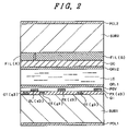
- FIG. 2 is a view showing a section on cut line 6 - 6 in FIG. 1
- FIG. 3 is a sectional view of the thin film transistor TFT on cut line 7 - 7 in FIG. 1
- FIG. 4 is a view showing a section of the storage capacitor Cstg on cut line 8 - 8 in FIG. 1 .
- thin film transistors TFT, storage capacitors Cstg and electrode groups are formed on a side of a lower transparent glass substrate SUB 1 while color filters FIL and shading black matrix patterns BM are formed on a side of an upper transparent glass substrate SUB 2 .
- the transparent glass substrates SUB 1 , SUB 2 have, on their inner surfaces (on the liquid crystal LC side), respective orientation films ORI 1 , ORI 2 to control initial alignment direction in the liquid crystal.
- the transparent glass substrates SUB 1 , SUB 2 have, on their outer surfaces, respective polarizing plates POL 1 , POL 2 .
- the thin film transistor TFT operates to decrease in channel resistance between a source and a drain when applied by a positive bias to a gate electrode GT, and increase in channel resistance between the source and the drain when the bias is rendered zero.
- the thin film transistor TFT has, as shown in FIG. 3 , a gate electrode GT, an insulator film GI, an i-type semiconductor layer AS formed of i-type (intrinsic, not doped with a conductivity determining impurity) amorphous silicon (Si), and a pair of a source electrode SD 1 and a drain electrode SD 2 .
- the source and drain in nature are determined by a bias polarity between them. It is to be understood that the source and drain are replaced with each other during operation because during operation the polarities thereof are to be inverted in the present liquid crystal display device circuit. In the below explanation, however, one is represented as a source and the other as a drain, for the sake of convenience.
- the gate electrode GT is formed continuing the scanning signal line GL, and structured such that part of the scanning signal line GL forms the gate electrode GT.
- the gate electrode GT is a part beyond an active region of the thin film transistor TFT.
- the gate electrode GT is formed by a single-layered conductor film g 3 .
- the conductor film g 3 uses a chromium-molybdenum alloy (Cr—Mo) film formed, for example, by sputtering, which however is not limitative. Alternatively, different kinds of metals may be formed in two layers.
- the scanning signal line GL is structured by a conductor film g 3 .
- the conductor film g 3 for the scanning signal line GL is formed in the same manufacturing process as the conductor film g 3 for the gate electrode GT, and structured integral therewith.
- a gate voltage (a scanning voltage) Vg is supplied from an external circuit to the gate electrode GT.
- the conductor film g 3 uses a chromium-molybdenum alloy (Cr—Mo) film formed, for example, by sputtering.
- the scanning signal line GL and the gate electrode GT are not limited to chromium-molybdenum alloy but may be in a two-layered structure having aluminum or aluminum alloy covered by cromium-molybdenum in order to reduce resistance. Furthermore, this line in an intersection with the image signal line DL is made thin in order to reduce the probability of short-circuit to the image signal line DL, or may be in a bifurcate form in order for being cut off by laser trimming in the event of short-circuiting.
- the counter voltage signal line CL is structured by a conductor film g 3 .
- the conductor film g 3 for the counter voltage signal line CL is formed in the same manufacturing process of the conductor film g 3 for the gate electrode GT, scanning signal line GL and counter electrode CT, and formed integral with the counter electrode CT.
- a counter voltage Vcom is supplied from an external circuit to the counter electrode CT.
- the counter voltage signal line CL is not limited to chromium-molybdenum alloy, but may be in a two-layered structure having aluminum or aluminum alloy covered by chromium-molybdenum in order to reduce resistance.
- this line in an intersection with the image signal line DL is made thin in order to reduce the probability of short-circuit to the image signal line DL, or may be in a bifurcate form for being cut off by laser trimming in the event of short-circuiting.
- the insulator film GI is used as a gate dielectric film of a thin film transistor TFT to provide, together with a gate electrode GT, electric field to a semiconductor layer AS.
- the insulator film GI is formed in an upper layer of the gate electrode GT and scanning signal line GL.
- a silicon nitride film formed for example by plasma CVD is selected and formed in a thickness of 2000 to 4500 angstroms (approximately 3500 angstroms in this embodiment).
- the insulator film GI serves also as an interlayer insulation film between the scanning signal line GL and counter voltage signal line CL and the image signal line DL, contributing to electric insulation for them.
- the i-type semiconductor layer AS is of amorphous silicon formed in a thickness of 150 to 2500 angstroms (a film thickness of approximately 1200 angstroms in this embodiment).
- a layer d 0 is an N(+) type amorphous silicon semiconductor layer doped with phosphorus (P) for ohmic contact, and left only in an area where an i-type semiconductor layer AS exists as an underlying layer and a conductor layer d 3 exists as an overlying layer.
- the i-type semiconductor layer AS and the layer d 0 are also provided both the intersections (crossover points) of the scanning signal line GL and counter voltage signal line CL and the image signal line DL.
- the i-type semiconductor layer AS at the interconnections reduces short-circuit between the scanning signal line GL and counter voltage signal line CL and the image signal line DL.
- the source electrode SD 1 and the drain electrode SD 2 are both structured by a conductor film d 3 in contact with the N(+) type semiconductor layer d 0 .
- the conductor film d 3 uses a chromium-molybdenum alloy (Cr—Mo) formed in a thickness of 500 to 3000 angstroms (approximately 2500 angstroms in this embodiment).
- the Cr—Mo film is low in stress and hence can be formed comparatively great in film thickness thus contributing to interconnect resistance decrease. Also, the Cr—Mo film is favorable in adhesion to the N(+) type semiconductor layer d 0 .
- the conductor film d 3 may use, besides a Cr—Mo film, a refractory metal (Mo, Ti, Ta, W) film or a refractory metal silicide (MoSi 2 , TiSi 2 , TaSi 2 , Wsi 2 ). Otherwise, a stack structure with aluminum or the like is satisfactory.
- the image signal line DL is structured by a conductor film d 3 in an same layer as the source electrode SD 1 and drain electrode SD 2 . Also, the image signal line DL is formed integral with the drain electrode SD 2 .
- the conductor film d 3 uses a chromium-molybdenum alloy (Cr—Mo) film formed by sputtering, and formed in a thickness of 500 to 3000 angstroms (approximately 2500 angstroms in this embodiment).
- the Cr—Mo film is low in stress and hence can be formed comparatively great in film thickness thus contributing to interconnect resistance decrease.
- the Cr—Mo film is favorable in adhesion to the N(+) type semiconductor layer d 0 .
- the conductor film d 3 may use, besides a Cr—Mo film, a refractory metal (Mo, Ti, Ta, W) film or a refractory metal silicide (MoSi 2 , TiSi 2 , TaSi 2 , Wsi 2 ). Otherwise, a stack structure with aluminum or the like is satisfactory.
- the conductor film d 3 is formed in a manner overlapping with the counter voltage signal line CL in an area of the source electrode SD 1 of the thin film transistor TFT. This overlap constitutes, as apparent from FIG. 5 , for the storage capacitor (electrostatic capacitor element) Cstg having the source electrode SD 1 (d 3 ) as one electrode and the counter voltage signal line CL as the other electrode.
- This storage capacitor Cstg has a dielectric film structured by the insulator film GI used as the gate insulation film for the thin film transistor TFT.
- the storage capacitor Cstg in planar is formed in part of the counter voltage signal line CL.
- a protective film PSV,PSV 1 is provided over the thin film transistor TFT.
- the protective film PSV,PSV 1 is formed mainly for protecting the thin film transistor from humidity or the like, and uses a material high in transparency and well in humidity resistance.
- the protective film PSV,PSV 1 is formed by a silicon oxide film or silicon nitride film formed, for example, in a plasma CVD apparatus, and formed in a film thickness of approximately 0.1 to 1 ⁇ m.
- the protective film PSV,PSV 1 is removed in a manner exposing external connection terminals DTM and GTM.
- the former is made thick in consideration of a protection effect and the latter the transistor mutual conductance gm is made thin.
- the protective film PSV,PSV 1 may be in a stacked structure with an organic film structured thick of polyimide or the like.
- the pixel electrode PX is formed integral with the source electrode SD 1 .
- the electrode is curved in a V-shaped in order to make different the electric field application direction EDR in between the region A and the region B as mentioned above.
- the counter electrode CT is formed integral with the counter electrode signal line CL.
- the electrode is curved in a V-shaped in order to make different the electric field application direction EDR in between the region A and the region B as mentioned above.
- the counter electrode CT is structured to be applied with a counter voltage Vcom.
- the counter voltage Vcom is set at a potential low by a feed through voltage ⁇ Vs to be generated upon turning the thin film transistor element TFT into off state from an intermediate current potential between a minimum level drive voltage Vdmin and a maximum level drive voltage Vdmax applied to the image signal line DL.
- an alternating current may be applied.
- a shade film BM (so-called a black matrix) is formed as a BM boundary line shown in FIG. 1 , in order not to emit the transmission light through unwanted gaps (gaps except for that between the pixel electrode PX and the counter electrode CT) toward a display surface and reduce the contrast ratio or the like.
- the shade film BM also plays a role of not allowing external light or backlight to be incident onto the i-type semiconductor layer AS. That is, the i-type semiconductor layer AS of the thin film transistor TFT is sandwiched by the upper and lower shade film BM and size-increased gate electrode GT thus being free from exposure by external natural light or backlight.
- each pixel region with light transmissive area defined by the shade film BM.
- the light transmissive area serves as a substantial pixel region.
- the shading film BM shown in FIG. 1 shows only one pixel but all the pixel are each formed with an aperture at an inside thereof. Also, this pattern is mere one example. In an area the direction of electric field disturbs at a comb-like electrode end or the like, the display at that area corresponds to in-pixel image information in a one-to-one relation wherein black is given in a case of black and white in a case of white. Accordingly, it is possible to utilize as part of display.
- the shade film BM must have shieldability against light. Particularly, in the gap between the pixel electrode PX and the counter electrode CT, optical concentration of 3 or higher is required in order to suppress crosstalk (vertical smear) in a direction of the image signal line. Also, although a conductive metal such as Cr may be used in formation, it is preferred to form with a highly-insulative film not to affect electric field present between the pixel electrode PX and the counter electrode CT. In the present embodiment, black organic pigment is mixed in resist material to form in a thickness of 1.2 ⁇ m.
- carbon, oxide titanium (T x O y ) may be mixed in a range that insulatability be kept at 10 8 ⁇ cm or higher without having an effect upon the electric field in a liquid crystal composition layer.
- the shade film BM partitions for effective display regions on each row and has a role to make distinct the contour of pixels on each row.
- a boundary line in a left-right direction in the figure is determined by the accuracy of aligning the upper and lower substrate. Where the alignment accuracy is higher than an electrode width of the counter electrode CT adjacent to the image signal line DL, setting in a width of the counter electrode enlarges the opening.
- the vertical boundary line to shade at least the area of the thin film transistor TFT while the boundary line in the left-right direction if set between a width of the counter electrodes on both sides of the image signal line can provides utmost improvement in opening ratio.
- the shade film BM is also formed in a picture frame form in a peripheral area, whose pattern is formed continuous with the matrix part pattern shown in FIG. 1 .
- the shade film BM in the periphery extends to an outside of a sealing area SL, preventing leak light such as reflection light resulting from mounting machine such as a personal computer from entering the matrix area and also light such as backlight from leaking outside the display area.
- this shade film BM is terminated at an inside by approximately 0.3 to 1.0 mm of an edge of the substrate SUB 2 and formed avoiding at cutting regions on the substrate SUB 2 .
- a color filter FIL is formed in a stripe form with repetition of red, green and blue in areas opposed to the pixels.
- the color filter FIL is formed in a manner overlapping with the area of the shade film BM.
- the color filter FIL can be formed in the following procedure. First, a pigment base material such as of acrylic resin is formed on the surface of the upper transparent substrate SUB 2 . Then, the pigment base material is removed in areas other than red filter forming areas by a photolithography technique. Thereafter, the pigment base material is dyed with a red pigment and subjected to a set process thus forming a red filter R. Next, similar processes are conducted to form a green filter G and a blue filter B in order. Incidentally, a dye may be used in dying.
- a pigment base material such as of acrylic resin is formed on the surface of the upper transparent substrate SUB 2 . Then, the pigment base material is removed in areas other than red filter forming areas by a photolithography technique. Thereafter, the pigment base material is dyed with a red pigment and subjected to a set process thus forming a red filter R. Next, similar processes are conducted to form a green filter G and a blue filter B in order. Incidentally, a dye may be used in dying
- An overcoat film OC is provided to prevent the dye of the color filter FIL from leaking into the liquid crystal composition layer LC and planarize the step caused by the color filter FIL and the shade film BM.
- the overcoat film OC is formed, for example, of a transparent resin material, e.g. an acrylic resin, an epoxy resin or the like. Also, the overcoat film OC may use an organic film such as polyimide well in fluidity.
- the liquid crystal composition LC employs a nematic liquid crystal having a dielectric constant anisotropy ⁇ .epsilon. in a positive value of 13.2 and refractivity anisotropy ⁇ n of 0.081 (589 nm, 20.degree. C.).
- the liquid crystal composition layer is in a thickness (gap) of 3.8 ⁇ m and a retardation ⁇ n.multidot.d of 0.31 ⁇ m.
- the retardation value ⁇ n.multidot.d is set between 0.25 ⁇ m and 0.35 ⁇ m, preferably between 0.28 ⁇ m and 0.32 ⁇ m, and combined with a hereinafter-referred orientation film and polarizing plate so that a maximum transmissivity can be obtained when liquid crystal molecules are turned from an initial alignment direction to an electric field direction by 45 degrees and transmission light almost free of wavelength dependency within a range of the visible portion of light can be obtained.
- the thickness (gap) of the liquid crystal composition layer is controlled by polymer beads processed of vertical orientation. This stabilizes the orientation of liquid crystal molecules around beads during black display thus obtaining favorable black level and improving contrast ratio.
- the liquid crystal material LC is not especially limited and the dielectric constant anisotropy ⁇ .epsilon. may be negative.
- the dielectric constant anisotropy ⁇ .epsilon. if greater in value can reduce drive voltage, and the refractivity anisotropy ⁇ n if smaller can increase the thickness (gap) of a liquid crystal layer thus shortening a liquid crystal filling time and reducing gap variation.
- the specific resistance of the liquid crystal composition uses a range of between 10 9 ⁇ and 10 14 ⁇ , preferably 10 11 ⁇ and 10 13 ⁇ .
- the voltage charged between the pixel electrode and the counter electrode can be sufficiently held wherein the lower limit is 10 9 ⁇ , preferably 10 11 ⁇ . This is because the pixel electrode and the counter electrode are structured on the same substrate.
- the resistance is excessively high, the static electricity introduced during manufacture process can be less reduced, it is preferably 10 14 ⁇ or less, preferably 10 13 ⁇ or less.
- the orientation film ORI uses polyimide.
- An initial alignment direction RDR is in parallel on the upper and lower substrate. Although the way for providing initial alignment direction is by rubbing, there is oblique evaporation as another.
- the relationship between an initial alignment direction RDR and an electric field application direction EDR is shown in FIG. 18 .
- the initial alignment direction RDR was provided as approximately 75 degrees with respect to a horizontal direction. This provides the region A of FIG. 1 with an angle 75 degrees defining between the initial alignment direction RDR and the electric field application direction EDR, and the region B with an angle 60 degrees defining between the initial alignment direction RDR and the electric field application direction EDR.
- the above values are not necessarily limitative in view of the object of the invention that the voltage for obtaining a maximum transmissivity in a voltage vs. luminance characteristic is low in the pixel region and a characteristic is made moderate around 10% of the relative transmissivity. It was confirmed satisfactory that in the region A the angle of between an electric field direction and an initial alignment direction is greater than 70 degrees in order to lower the voltage of obtaining a maximum transmissivity and in the B region the angle between an electric field direction and an initial alignment direction is within a range of between 30 degrees and 75 degrees in order to moderate the characteristic at around a relative transmissivity of 10%.
- the angle of between an initial alignment direction RDR and an electric field application direction EDR if the liquid crystal material has a positive dielectric constant anisotropy ⁇ .epsilon. should be less than 90 degrees and if a negative dielectric constant anisotropy ⁇ .epsilon. exceed 0 degree.
- this embodiment formes, for each pixel region, the region B by bending the pixel electrode PX and counter electrode CT extending in the region A, as shown in FIG. 1 .
- a similar effect is to be obtained by working part of the orientation film ORI.
- the pixel region structure on the transparent substrate SUB 1 has no devising on the pixel electrode PX and counter electrode CT. Rather, as shown in FIG. 24B , the orientation film ORI in an area corresponding to the B region in the pixel region is given an initial alignment direction different from that in the region A.
- rubbing is conducted over the entire area in a direction of initial alignment as set in the region A.
- a photoresist film is formed all over the rubbed surface to form an opening in an area corresponding to the region B by a well-known photolithography technique.
- rubbing is conducted in a predetermined direction (in a direction different from the initial alignment direction) over the surface of the photoresist film thereby rubbing the polyimide in an exposed area (region B) from the opened photoresist film. Then, the photoresist film is removed away.
- the respective ones of electrode width of the pixel electrode PX and the counter electrode CT in the region B are made greater than those in the region A so that a predetermined voltage vs. luminance characteristic can be easily obtained by controlling the spacing between the pixel electrode PX and the counter electrode CT due to the control in the electrode width.
- the polarizing plate POL uses a polarizing plate having a conductivity.
- the lower polarizing plate POL 1 is put coincident in polarizing transmission axis MAX 1 with the initial alignment direction RDR while the upper polarizing plate POL 2 in polarizing transmission axis MAX 2 is in orthogonal thereto.
- FIG. 18 shows a relationship of the same. Due to this, a normally close characteristic is obtainable that the transmissivity increases with increase in the voltage applied to the pixel of the invention (voltage between the pixel electrode PX and the counter electrode CT). Also, when no voltage is applied, a high quality black display is possible.
- a countermeasure is done against poor display due to external static electricity and EMI by providing conductivity to the polarizing plate.
- Concerning conductivity it is preferred to give a sheet resistance of 10 8 ⁇ /.quadrature. or less for only coping with the affection of static electricity, or 10 4 ⁇ /.quadrature. or less if coping also with EMI.
- a conductor layer may be provided on a backside of a surface of the glass substrate sandwiching the liquid crystal composition (surface to be adhered with the polarizing plate).
- FIG. 5 is a figure illustrating a plan of an essential part around the matrix (AR) of the display panel PNL including upper and lower glass substrates SUB 1 and SUB 2 .
- FIG. 6 is a figure illustrating on a left side a section of around an external connection terminal GTM to be connected with a scanning circuit and on a right side a section of around a seal part where no external connection terminal exists.
- FIG. 5 and FIG. 6 illustrate an example of the latter.
- FIG. 5 and FIG. 6 both depict upper and lower substrate SUB 1 , SUB 2 after cut wherein LN represents the before-cut edges for the both substrates.
- the upper substrate SUB 2 in size is limited inward of the lower substrate SUB 1 in a manner exposing them.
- the terminal groups Tg, Td are named collectively in plurality to a unit of a tape carrier package TCP mounted with an integrated circuit chip CHI for a scanning circuit connection terminal GTM, image signal circuit connection terminal DTM, described later, and their extension wiring.
- the extension wiring from a matrix of each group to the external connection terminal is made slant as an end is neared.
- a counter electrode terminal CTM is a terminal to deliver a counter voltage from an external circuit to the counter electrode CT.
- the counter voltage signal line CL in the matrix is extended on an opposite side (on the right side in the figure) of the scanning circuit terminal GTM so that each counter voltage signal line is collected on the common bus line CB and connected to the counter electrode terminal CTM.
- a seal pattern SL is formed along edges thereof except for a liquid-crystal injection port INJ in a manner sealing a liquid crystal LC.
- the seal member is formed, for example, of epoxy resin.
- the orientation film ORI 1 , ORI 2 layers are each formed at an inner side of the seal pattern SL.
- the polarizing plates POL 1 , POL 2 are respectively structured on outer surfaces of the lower transparent glass substrate SUB 1 and the upper transparent glass substrate SUB 2 .
- the liquid crystal LC is filled in a region partitioned by the seal pattern SL between the lower orientation film ORI 1 and upper orientation film ORI 2 for setting an orientation of liquid crystal molecules.
- the lower orientation film ORI 1 is formed on a protection film PSV 1 on a side of the lower transparent glass substrate SUB 1 .
- This liquid crystal display device is assembled by laying various layers separately on the lower transparent glass substrate SUB 1 side and the upper transparent glass substrate SUB 2 side, forming a seal pattern SL on the substrate SUB 2 side, putting together the lower transparent glass substrate SUB 1 and the upper transparent glass substrate SUB 2 , injecting a liquid crystal LC through the opening INJ of the seal member SL, sealing the injection port INJ by epoxy resin or the like, and cutting the upper and lower substrate.
- FIG. 7 is a view illustrating a connection structure of from a scanning signal line GL for the display matrix to an external connection terminal GTM thereof, wherein (A) is a plan view and (B) shows a section on cut line B-B in (A). Incidentally, the same figure corresponds to a lower portion of FIG. 5 .
- An oblique wiring part is represented by a straight line form for the sale of convenience.
- a gate terminal GTM is structured by a Cr—Mo layer g 3 and further a transparent conductor layer i 1 for protecting a surface thereof and improving the reliability in connection to a TCP (Tape Carrier Package).
- the transparent conductor layer i 1 uses a transparent conductor film ITO.
- an insulator film GI and protection film PSV 1 are formed on a right side of a boundary line thereof.
- a terminal GTM positioned at a left end is exposed from them and allowed to have electric contact with an external circuit.
- the figure illustrates one pair of a gate line GL and a gate terminal, actually a plurality of such pairs are vertically arranged to constitute a terminal group Tg ( FIG. 5 ).
- the gate terminal at its left end in manufacture process extends across a cut region of the substrate and is short-circuited by an interconnection SHg (not shown). This is helpful in preventing against electrostatic breakdown during rubbing the orientation film ORI 1 in the manufacture process.
- FIG. 8 is a view illustrating a connection from the image signal line DL to the externally connection terminal DTM thereof, wherein (A) shows a plan and (B) illustrates a section on cut line B-B in (A). Incidentally, the same figure corresponds to an upper right part and its vicinity of FIG. 5 . Although the orientation of the figure is changed for the convenience sake, a right end direction corresponds to an upper end of the substrate SUB 1 .
- TSTd is an inspection terminal. This is not connected with an external circuit but widened in width to allow contact by a probe needle or the like. Similarly, a drain terminal DTM is also widened in width in order for connection with an external circuit.
- the external connection drain terminal DTM is provided in a vertical direction.
- the drain terminal DTM as shown in FIG. 5 , constitutes for a terminal group Td (suffix omitted) and extends beyond a cut line on the substrate SUB 1 . In the manufacture process, they are all short-circuited one another by an interconnection SHd (not shown) in order to prevent against electrostatic breakdown.
- the inspection terminal TSTd is formed on every other one of an image signal line DL, as shown in FIG. 8 .
- the drain connection terminal DTM is formed of a transparent conductor layer i 1 and connected, in an area removed of a protection film PSV 1 , with an image signal line DL.
- the transparent conductor film i 1 uses a transparent conductor film ITO similarly to that of the gate terminal GTM.
- the extension line of from the matrix to the drain terminal DTM is structured with a layer d 3 in a same level as the image signal line DL.
- FIGS. 9A and 9B are views illustrating a connection of from a counter voltage signal line CL to an external connection terminal CTM thereof, wherein FIG. 9A shows a plan and FIG. 9B a sectional view on cut line B-B in FIG. 9A . Incidentally, the same figure corresponds to an upper left portion and its vicinity of FIG. 5 .
- Each counter voltage signal line CL is collected on the common bus line CB 1 and extended to the counter electrode terminal CTM.
- the common bus line CB 1 is structured by laying a conductor layer d 3 on a conductor layer g 3 and electrically connecting them by a transparent conductor layer i 1 . This is to reduce the resistance on the common bus line CB and sufficiently supply a counter voltage from an external circuit to each counter voltage signal line CL.
- the present structure is characterized in that the resistance on the common bus line can be reduced without especially imposing new load on the conductor layer.
- the counter electrode terminal CTM is structured having a transparent conductor layer i 1 laid on the conductor layer g 3 .
- This transparent conductor film i 1 uses a transparent conductor film ITO similarly to that of other terminals.
- the transparent conductor layer i 1 protects a surface.
- the conductor layer g 3 is covered by the transparent conductor layer i 1 having endurance to prevent electrolytic corrosion, etc.
- the connection of the transparent conductor layer i 1 to the conductive layer g 3 and conductor layer d 3 is made by providing conduction of a through-hole formed in the protection film PSV 1 and insulator film GI.
- FIGS. 10A and 10B are views illustrating a connection of from the other end of the counter voltage signal line CL to an external connection terminal CTM 2 thereof, wherein FIG. 10A shows a plan and FIG. 10B a section on cut line B-B in FIG. 10A . Incidentally, the same figure corresponds to the upper right portion and its vicinity of FIG. 5 .
- each counter voltage signal line CL at the other end is collected and extended to the counter electrode terminal CTM 2 .
- the different point from the common bus line CB 1 is formation with a conductor layer d 3 and transparent conductor layer i 1 so as to be insulated from the scanning signal line GL. Also, insulation is provided by an insulator film GI from the scanning signal line GL.
- FIG. 11 illustrates a connection diagram of a display-matrix equivalent circuit and its peripheral circuits. The same figure as a circuit diagram is depicted corresponding to an actual geometric arrangement.
- AR is a matrix array having a plurality of pixels arranged in a two-dimensional form.
- X means an image signal line DL and suffixes G, B and R are added corresponding to green, blue and red pixels.
- Y means a scanning signal line GL having a suffix 1, 2, 3, . . . , end according to a sequence in timing of scanning.
- Scanning signal lines Y (suffix omitted) are connected to a vertical scanning circuit V
- image signal lines X (suffix omitted) are connected to an image signal drive circuit H.
- SUP is a circuit including a power circuit to obtain a plurality of stabilized power sources voltage-divided from one power supply and circuit to exchange information for CRT (cathode ray tube) from host (host central processing unit) to information for TFT liquid crystal display device.
- CRT cathode ray tube
- host host central processing unit
- FIGS. 12A through 12F illustrate drive waveforms for the liquid crystal display device of the present embodiment.
- a counter voltage Vch is given a constant voltage.
- a scanning signal Vg is on in level every one scanning period and off in level in other timing.
- An image signal voltage is double in amplitude of a voltage to be applied to the liquid crystal layer and inverted in positive and negative pole every one frame, being applied in a manner conveyed to one pixel.
- the image signal voltage Vd is inverted in polarity on every one column and also inverted in polarity on every other row. This provides a structure having polarity-inverted pixels adjacent in the upper, lower, left and right, wherein flicker, crosstalk (smear) is not liable to occur.
- a counter voltage Vc is set at a voltage lowered by a given amount from a center voltage of polarity inversion in the image signal voltage. This is to correct a field-through voltage to be occurred upon turning from on to off in the thin film transistor element, and to apply an alternating current with a reduced direct current component to the liquid crystal (because the liquid crystal is increased in residual image, deterioration, etc. if applied with a direct current).
- the counter voltage if made alternating, can be reduced in maximum amplitude in the image signal voltage, making it possible to use an image signal drive circuit (signal side driver) with a low withstand voltage.
- a conductor film g 3 of Cr—Mo or the like is provided by sputtering to a film thickness of 2000 angstroms over a lower transparent glass substrate SUB 1 of AN635-glass (product name).
- the conductor film g 3 is selectively etched using cerium nitrate ammonia. This forms a gate electrode GT, a scanning signal line GL, a counter voltage signal line CL, a counter electrode CT, a gate terminal GTM, a first conductor layer of a common bus line CB 1 , a first conductor layer in the counter electrode terminal CTM 1 , a bus line SHg for connecting the gate terminal GTM (not shown).
- a hydrogen gas and a phosphine gas are introduced in the plasma CVD apparatus to provide an N(+) type amorphous Si film with a film thickness of 300 angstroms.
- SF 6 and CC 14 are used as dry etching gases to preferentially etch the N(+) type amorphous Si film and i-type amorphous Si film, thereby forming an i-type semiconductor layer AS island.
- a Cr conductor film d 3 with a film thickness of 300 angstroms is provided by sputtering.
- the conductor film d 3 is etched with a solution similar to that of the process A, thus forming an image signal line DL, a source electrode SD 1 , a pixel electrode PX, a drain electrode SD 2 , a first conductor layer in a common bus line CB 2 and a bus line SHd short-circuiting the drain terminal DTM (not shown).
- CC 14 and SF 6 are introduced in a dry etching apparatus to etch the N(+) type amorphous Si film thereby selectively remove the N(+) type semiconductor layer d 0 from between the source and the drain.
- the conductor film d 3 is patterned with a mask pattern, the N(+) type semiconductor layer d 0 is removed using the conductor film d 3 as a mask. That is, the N(+) type semiconductor layer d 0 left on the i-type semiconductor layer AS is removed at areas other than the conductor film d 1 and the conductor film d 2 in a self-aligned manner. At this time, the N(+) type semiconductor layer d 0 is etched such that it in the entire thickness is completely etched. Accordingly, the i-type semiconductor layer AS in its surface is somewhat etched, the degree of which may be controlled by etching time.
- An ammonia gas, a silane gas and nitrogen gas are introduced in the plasma CVD apparatus to provide a Si nitride film in a film thickness of 0.4 ⁇ m.
- SF 6 is used as a dry etch gas to preferentially etch the Si nitride film thereby patterning the protection film PSV 1 and insulator film GI.
- the protection film PSV 1 and the insulator film GI are patterned by a same photo-mask and formed at a same time.
- a transparent conductor film i 1 of an ITO film is provided by sputtering in a film thickness of 1400 angstroms. After a photolithography process, the transparent conductor film i 1 is preferentially etched using an acid mixture solution of a hydrochloric acid and a nitric acid as an etch solution, thereby forming an uppermost layer for a gate terminal GTM, a drain terminal DTM and second conductor layers for counter electrode terminals CTM 1 and CTM 2 .
- FIG. 16 is a top view illustrating a state that the display panel PNL shown in FIG. 5 , etc. is connected with an image signal drive circuit H and a vertical scanning circuit V.
- CHI is a drive IC chip for driving the display panel PNL (lower five are drive IC chips on a vertical scanning circuit side, and left ten in each are a drive IC chip on a image signal drive circuit side).
- TCP is a tape carrier package having a driving IC chip CHI mounted thereon by a tape automated bonding (TAB) method.
- PCB 1 is a driving circuit board mounted with the TCP or capacitors, etc. and divided into two for an image signal drive circuit and a scanning signal drive circuit.
- FGP is a frame ground pad and soldered with a spring-formed piece provided by cut on a shield case SHD.
- FC is a flat cable for electrical connection between the driving circuit board PCB 1 on a lower side and the driving circuit board PCB 1 on a left side.
- the flat cable FC uses one having a plurality of lead wires (a phosphor bronze material plated with Sn) held sandwiched by a stripe formed polyethylene layer and polyvinylalchol layer as shown in the figure
- FIG. 17 is an exploded perspective view illustrating component parts for a liquid crystal display module MDL.
- SHD is a frame-formed shield case (metal frame) made by a metal plate
- LCW is a display window
- PNL is a liquid crystal display panel
- SPB is a light diffuser plate
- LCB is a light conductor member
- RM is a reflector plate
- BL is a backlight fluorescent tube
- LCA is a backlight case.
- the members are stacked in a relationship of vertical arrangement as shown in the figure thereby assembling a module MDL.
- the module MDL in its entirety is fixed by a pawl and hook provided on the shield case SHD.
- the backlight case LCA is made in a form to accommodate therein the backlight fluorescent tube BL, the light diffuser plate SPB light diffuser plate, the light conductor member LCB and the reflector plate RM.
- the light of the backlight fluorescent tube BL arranged on a side face of the light conductor member LCB is turned by the light conductor member LCB, reflector plate RM and light diffuser plate SPB into homogeneous backlight on a display surface, being emitted to a liquid crystal display panel PNL side.
- the backlight fluorescent tube BL is connected with an inverter circuit board PCB 3 serving as a power source for the backlight fluorescent tube BL.
- FIG. 21 is a graph showing an electro-optical characteristic (voltage vs. luminance characteristic) of a liquid crystal display device constructed as above.
- this graph includes illustrations of a voltage vs. luminance characteristic A only in the region A and a voltage vs. luminance characteristic B only in the region B, and the voltage vs. luminance characteristic of the liquid crystal display apparatus according to the present embodiment is shown as a combination of them, i.e. A+B in the figure.
- the voltage vs. luminance characteristic B in the region B is for a case as shown in FIG. 1 that the spacing between the pixel electrode PX and the counter electrode in the region B is narrowed than that in the region A.
- a characteristic shifted in a voltage direction is obtained (narrowing the spacing between the electrodes results in shift leftward of the graph).
- the voltage vs. luminance characteristic A only in the region A has a range that luminance changes steeply with respect to voltage. However, this range can be made moderate by providing the region B having a voltage vs. luminance characteristic B.
- the range that luminance steeply changes with respect to voltage exists conspicuously in the vicinity of a transmissivity of 10 in a darker middle tone range (transmissivity 0-20%), in which range moderateness is given.
- the region B is effectively provided for a case in a range of 0.05 to 0.3 times the area of the region A.
- the effect can be provided without the increase of a maximum drive voltage Vmax to between the pixel electrode PX and the counter voltage CT.
- the maximum drive voltage Vmax is suppressed from increasing.
- the region B by providing a range of an angle .PHI. LC of between 30 and 75 degrees defining between the electric field direction and the initial alignment direction (preferably between 45 and 60 degrees), the rise in luminance can be put to a lowermost voltage.
- the region A is to suppress from rising the voltage applied between the pixel electrode PX and the counter electrode CT described above.
- the area ratio of the region A and region B is not especially limitative. There is no technical reason of necessarily providing the application voltage to between the pixel electrode PX and the counter electrode CT to a predetermined value or lower, because it can be properly determined from a relationship of between an obtainable application voltage and moderate characteristic curve.
- the region B is satisfactorily provided having an electric field direction and initial orientation direction different in the angle relative to the region A set in angle defined between an electric field direction and an initial alignment direction in an area between the pixel electrode PX and the counter electrode CT.
- the provision of the region B gives the voltage vs. luminance characteristic with a more moderate curve than in the pixel region only in the region A thereby reducing the variation in luminance due to the variation in electrode-to-electrode spacing.
- the effect of the invention is similarly obtainable by means for regulating an initial alignment direction of liquid crystal, i.e. in a case of giving the improvement described above only to the orientation film ORI.
- the invention has a region A and region B in a pixel region, and lies in that in the region B the angle defined between an electric field direction and an initial alignment direction is given different from that in the region A.
- the initial alignment direction in the region B may be given different from that in the region A.
- the electric field direction and initial alignment direction in the region B may be respectively made different from those in region A with a result that the angle defined between the electric field direction and initial alignment direction in the region B be different from that in the region A. This of course provides a similar effect.
- the invention is also applicable in a viewpoint that, where the voltage vs. luminance characteristic in the pixel region in part is steep, that point is made moderate to improve the quality of display.
- the invention is not necessarily premised on a presence of variation in the spacing of between the counter electrode CT and the pixel electrode PX.
- a middle tone range (range having an optical transmissivity of 0-20%) as one point where the pixel-region voltage vs. luminance characteristic assumes steep.
- FIG. 25 is a structural view illustrating another embodiment of a liquid crystal display device according to the invention. Incidentally, a sectional view on line 7 - 7 in the figure is similar to FIG. 3 .
- This figure shows a plan structure of a matrix (pixel part).
- the parts other than this are similar to the case of Embodiment 1.
- the present embodiment has a difference in that a counter voltage signal line CL is formed extending in almost a center of each pixel region in a manner separating same and the spacing between the pixel electrode PX and the counter electrode CT is varied in areas corresponding to the region A and region B.
- scanning signal lines GL extending right-and-left are vertically formed on a main surface of a transparent substrate SUB 1 . Between the scanning signal lines GL a counter voltage signal line CL is formed extending also in the right-and-left direction.
- the scanning signal line GL and the counter voltage signal line CL are structured, for example, of a same material, which are formed simultaneously.
- the pixel region is constituted by an area encompassed by the scanning signal lines GL and adjacent image signal lines DL, hereafter stated. Due to this, the counter voltage signal line CL is formed almost in the center of the pixel region.
- This structure is to separate the counter voltage signal line CL from the scanning signal line GL and thereby avoid them from being formed in contact during manufacture.
- the upper and lower area of the pixel region i.e. the area adjacent to the each scanning signal line GL, is structured as a region B with the remaining area as a region A.
- the structural difference in between these areas will be apparent hereafter.
- the counter voltage signal line CL is formed integral with a counter electrode CT extending within each pixel region.
- the counter electrode CT vertically extends sandwiching the counter voltage signal line CL.
- Three counter electrodes CT in total are structured, i.e. one is adjacent to one image signal line DL, one adjacent to the other image signal line DL, and one between them.
- this embodiment has an especial shape in an area that each counter electrode CT is adjacent to the scanning signal line GL (region B in the pixel region).
- the left two for example have portions protruding right. This allows to form an electrode spacing to the hereafter-referred pixel electrode PX to be positioned right smaller than that of the region A.
- the right two for example have portions protruding left. This allows to form an electrode spacing to the hereafter-referred pixel electrode PX to be positioned left smaller than that of the region A.
- an insulator film GI (see FIG. 3 ) is formed covering the scanning signal lines GL and the counter voltage signal lines CL (counter electrodes CT).
- This insulator film GI serves as a gate insulation film for the hereafter-referred image signal line DL and for the scanning signal line GL and counter voltage signal line CT, a gate insulation film for an area to form a thin film transistor TFT, and a dielectric film for an area to form a storage capacitor Cstg.
- amorphous silicon AS is formed in an area to form a thin film transistor TFT.
- the amorphous silicon AS is formed superposed on the scanning signal line GL in an area close to the image signal line DL.
- the scanning signal line GL in part is structured serving also as a gate electrode GT of a thin film transistor TFT.
- an image signal line DL extending in the vertical direction and juxtaposed with respect to the right-and-left direction.
- This image signal line DL is provided with a drain electrode SD 2 formed extending to one part of a surface of the amorphous silicon AS for the thin film transistor TFT.
- a pixel electrode PX is formed of a same material as and simultaneous with the image signal line DL.
- This pixel electrode PX is formed in a manner running between the counter electrodes CT.
- the pixel electrode PX has a common connection point PXC formed superposed on part of the counter voltage signal line CT.
- Totally two pixel electrodes PX are structured such that one is in a manner running between the two counter electrodes CT arranged adjacent on a left side in the figure and one is in a manner running between the two counter electrodes CT arranged adjacent on a right side in the figure.
- the pixel electrode PX thus structured is formed almost in an ‘H’ shape including the common connection point, one of ends of which extends to the area of forming a thin film transistor TFT and structures a source electrode SD 1 for the thin film transistor TFT.
- this embodiment has an especial form in an area where each pixel electrode PX nears the scanning signal line GL (region B in the pixel region).
- the two extending upward beyond the common connection points PXC have right-protruding portions. This allows to form an electrode spacing to the counter electrode CT to be positioned right smaller than that in the region A.
- the right one has a left-protruding portion. This allows to form an electrode spacing to the counter electrode CT to be positioned left smaller than that in the region A.
- an electric field occurring there in direction has an angle with respect to an electric field direction in the region A.
- a substantial region B is formed.
- the portion formed with an electrode protrusion and the portion not so formed have a boundary in a hatched continuous form. It is needless to say that a region B is to be formed from the above-stated reason even for a stepwise connected form (the portion formed with a protrusion and the portion not so formed have an angle of 90 degrees between them).
- the common connection point PXC to the pixel electrode PX in an area superposed over the counter voltage signal line CT cooperates with the counter voltage signal line CT to structure therebetween a storage capacitor Cstg having the insulator film as a dielectric film.
- This storage capacitor Cstg provides an effect of storing image information on the pixel electrode PX, for example, when the thin film transistor TFT is off.
- phosphorus (P) is doped to a surface of the amorphous silicon AS corresponding to an interface between a drain electrode SD 2 and a source electrode SD 1 of the thin film transistor TFT mentioned before, into a high concentration layer.
- the amorphous silicon As has the high concentration layer formed over an entire surface thereof. After forming each electrode, the electrode is used as a mask to etch the high concentration layer in areas other than the electrode forming area, thereby making it possible to provide the above structure.
- a protection film PSV e.g. of a silicon nitride film, (see FIG. 3 ) is formed over a surface of the insulator film GI thus formed with the thin film transistors TFT, image signal lines DL, pixel electrodes PX and storage capacitors Cstg.
- An orientation film is formed on a surface of the protection film PSV.
- the transparent substrate SUB 1 thus structured is to be oppositely arranged, through a liquid crystal, with a transparent substrate SUB 2 as the other substrate having a surface on the liquid crystal side formed with a black matrix BM and color filters FIL, etc.
- the black matrix BM is satisfactorily formed to cover at least a gap of between an area of forming a thin film transistor TFT and image signal line DL and the adjacent counter electrode CT. This is because the thin film transistor TFT if having light illumination changes in its property causing light leak in the gap between the image signal line DL and the counter electrode CT. This situation is true for the case of Embodiment 1.
- FIG. 26 is a graph illustrating a B (transmissivity: luminance) vs. V (voltage between the counter electrode and the pixel electrode) characteristic in each pixel of a liquid crystal display device structured as above.
- characteristic are shown in order for cases as: characteristic where the invention is not applied (reference), characteristics where in a sub-pixel region (region B) the electrode spacing and opening area ratio are respectively given (6 ⁇ m, 10%), (5 ⁇ m, 5%), (4 ⁇ m, 5%) and (3 ⁇ m, 5%).
- the sub-pixel opening area ratio refers to a ratio of a sub-pixel area to one-pixel area.
- FIG. 27 is a graph illustrating a B vs. V characteristic where in the sub-pixel of the pixel (region B) the spacing between the counter electrode and the pixel electrode is varied in a liquid crystal display device structured as above.
- FIG. 28 is a graph illustrating a B vs. V characteristic where the invention is not applied but the spacing between the counter electrode and the pixel electrode is varied. Illustrated are cases that the spacing between the counter electrode and the pixel electrode is varied respectively by .+ ⁇ 0.1.0 ⁇ m.
- the counter electrode CT and the pixel electrode PX are formed in parallel with the image signal line DL.
- the invention is not limited to this.
- the counter electrode CT and the pixel electrode PX be in parallel with the image signal line DL as shown, for example, in FIG. 29 .
- the region A and the region B were provided in a manner dividing the pixel region, this is not necessarily limitative. It is needless to say that a similar effect is obtainable if there exist a plurality of regions A and regions B and these regions be formed in a mixed state.
- FIG. 30 is another embodiment having a structure having a region B provided nearly in a center of a light transmissive area in the pixel region, which is a figure corresponding, for example, to FIG. 23 .
- a region B is formed by forming an area comparatively wide in linewidth nearly in a center of the pixel electrode PX.
- the pixel electrode PX is formed with a part narrowed in distance to an adjacent counter electrode CT, in a vicinity of which a part will be formed having an electric field direction different from an electric field direction of a region A as another region.
- FIG. 32A is a magnifying view of this part wherein the direction of an electric field is shown by arrows given between the pixel electrode PX and the counter electrode CT.
- the formation of a width-increased portion in the pixel electrode forms an area different in electric field direction. This area serves as a region B.
- this embodiment forms a comparatively widened linewidth area in the pixel electrode PX, it is needless to say that a similar effect is obtainable by providing a similar structure in the counter electrode CT.
- the structure shown, for example, in FIG. 23 may be adopted together.
- the region B will exist in a divided state in respective light transmissive areas in the pixel region.
- FIG. 31 is a structural view showing still another embodiment.
- the domain DM is an area where an electric field occurs, for example, in a coincident direction with an axial direction of initially-oriented liquid crystal molecules, wherein the liquid crystal molecules if applied by an electric field will not twist, thus resulting in out of control in light transmissivity.
- FIG. 31 is a view illustrating an embodiment to eliminate such a disadvantage, wherein the area where a domain DM is to occur is masked with a counter voltage signal line CL.
- FIG. 25 or FIG. 29 corresponds to FIG. 25 or FIG. 29 .
- a pixel electrode PX formed intersecting a counter voltage signal line CL through an insulation film the intersection is formed with an increased linewidth part (protrusion).
- the storage capacity Cstg is secured in the increased linewidth area in the pixel electrode PX.
- the pixel electrodes PX in plurality are connected common in the part close to the scanning signal line GL (upper in the figure). As a result, the pixel electrode is formed in a squared-U form.
- the method for masking for the Domain DM includes a method of masking with a black matrix BM. This structure may be made.
- the structure shown, for example, in FIG. 25 or FIG. 29 may be adopted together.
- the region B will exist in a divided state in respective light transmissive areas in the pixel region.
- a liquid crystal display device in a liquid crystal display device of a lateral electric field scheme realizable a viewing angle in a Braun tube level, a liquid crystal display device can be provided which has a favorable image quality with even luminance but less unevenness of luminance even when the electrode spacing varies due to variation in photolithography or etching in forming electrodes.
Abstract
Description
Claims (13)
Priority Applications (1)
| Application Number | Priority Date | Filing Date | Title |
|---|---|---|---|
| US11/373,292 US7599031B2 (en) | 1998-03-06 | 2006-03-13 | Liquid crystal display device |
Applications Claiming Priority (7)
| Application Number | Priority Date | Filing Date | Title |
|---|---|---|---|
| JP5454498 | 1998-03-06 | ||
| JP10-54544 | 1998-03-06 | ||
| PCT/JP1998/002945 WO1999045430A1 (en) | 1998-03-06 | 1998-06-30 | Liquid crystal display |
| WOPCT/JP98/02945 | 1998-06-30 | ||
| US61010200A | 2000-06-30 | 2000-06-30 | |
| US10/462,603 US20040109103A1 (en) | 1998-06-30 | 2003-06-17 | Liquid crystal display device |
| US11/373,292 US7599031B2 (en) | 1998-03-06 | 2006-03-13 | Liquid crystal display device |
Related Parent Applications (1)
| Application Number | Title | Priority Date | Filing Date |
|---|---|---|---|
| US10/462,603 Continuation US20040109103A1 (en) | 1998-03-06 | 2003-06-17 | Liquid crystal display device |
Publications (2)
| Publication Number | Publication Date |
|---|---|
| US20060152661A1 US20060152661A1 (en) | 2006-07-13 |
| US7599031B2 true US7599031B2 (en) | 2009-10-06 |
Family
ID=32469772
Family Applications (2)
| Application Number | Title | Priority Date | Filing Date |
|---|---|---|---|
| US10/462,603 Abandoned US20040109103A1 (en) | 1998-03-06 | 2003-06-17 | Liquid crystal display device |
| US11/373,292 Expired - Fee Related US7599031B2 (en) | 1998-03-06 | 2006-03-13 | Liquid crystal display device |
Family Applications Before (1)
| Application Number | Title | Priority Date | Filing Date |
|---|---|---|---|
| US10/462,603 Abandoned US20040109103A1 (en) | 1998-03-06 | 2003-06-17 | Liquid crystal display device |
Country Status (1)
| Country | Link |
|---|---|
| US (2) | US20040109103A1 (en) |
Families Citing this family (6)
| Publication number | Priority date | Publication date | Assignee | Title |
|---|---|---|---|---|
| US20040109103A1 (en) * | 1998-06-30 | 2004-06-10 | Hitachi, Ltd. | Liquid crystal display device |
| WO2001095023A1 (en) * | 2000-06-08 | 2001-12-13 | Matsushita Electric Industrial Co., Ltd. | Image display and method for displaying image |
| KR101082909B1 (en) * | 2005-02-05 | 2011-11-11 | 삼성전자주식회사 | Gate driving method and gate driver and display device having the same |
| KR101309779B1 (en) * | 2005-09-06 | 2013-09-25 | 삼성디스플레이 주식회사 | Liquid crystal display |
| JP4585411B2 (en) * | 2005-09-12 | 2010-11-24 | 株式会社 日立ディスプレイズ | Transmission type liquid crystal display device |
| CN104062818B (en) * | 2014-06-27 | 2017-10-24 | 上海天马微电子有限公司 | A kind of Liquid crystal disply device and its preparation method |
Citations (55)
| Publication number | Priority date | Publication date | Assignee | Title |
|---|---|---|---|---|
| US4846560A (en) | 1985-09-13 | 1989-07-11 | Canon Kabushiki Kaisha | Liquid crystal device with ferroelectric liquid crystal oriented at non-pixel portions |
| US5192596A (en) | 1989-06-02 | 1993-03-09 | Canon Kabushiki Kaisha | Liquid crystal device |
| US5426526A (en) | 1991-04-05 | 1995-06-20 | Sharp Kabushiki Kaisha | Reflection type single crystal silicon substrate liquid crystal display device and system |
| JPH07244292A (en) | 1994-03-03 | 1995-09-19 | Mitsubishi Electric Corp | Thin-film transistor substrate and its production and production of liquid crystal display device |
| JPH08313923A (en) | 1994-09-17 | 1996-11-29 | Toshiba Corp | Liquid crystal display element |
| EP0749029A1 (en) | 1995-06-14 | 1996-12-18 | Hitachi, Ltd. | Liquid crystal display device with wide viewing angle characteristics comprising a high resistivity black matrix |
| JPH09101538A (en) | 1995-10-04 | 1997-04-15 | Hitachi Ltd | Active matrix type liquid crystal display device and its production |
| EP0805374A2 (en) | 1996-05-01 | 1997-11-05 | Stanley Electric Co., Ltd. | Liquid crystal display of horizontal field type |
| JPH103092A (en) | 1996-06-14 | 1998-01-06 | Oobayashi Seiko Kk | Liquid crystal display device |
| WO1998008136A1 (en) | 1996-08-22 | 1998-02-26 | Hoechst Research & Technology Deutschland Gmbh & Co. Kg | Liquid crystal display device |
| US5729307A (en) | 1994-10-25 | 1998-03-17 | Sharp Kabushiki Kaisha | Antiferroelectric LCD in which a normal to an antiferroelectric liquid crystal layer is orthogonal to a normal to a second antiferroelectric liquid crystal layer |
| US5781262A (en) | 1994-04-19 | 1998-07-14 | Nec Corporation | Liquid crystal display cell |
| US5805247A (en) | 1995-10-26 | 1998-09-08 | Hitachi, Ltd. | Liquid crystal display apparatus in which plural common electrodes are parallel to the pixel electrodes on the same substrate and a black matrix on the opposing substrate |
| US5831707A (en) | 1994-08-24 | 1998-11-03 | Hitachi, Ltd. | Active matrix type liquid crystal display apparatus |
| US5844643A (en) | 1995-09-14 | 1998-12-01 | Sharp Kabushiki Kaisha | Liquid crystal display device with at least 7° C. liquid crystal to isotropic phase transition temperature difference and method of making |
| US5872611A (en) | 1993-07-27 | 1999-02-16 | Sharp Kabushiki Kaisha | Liquid crystal display having two or more spacings between electrodes |
| US5922242A (en) * | 1996-05-20 | 1999-07-13 | Kabushiki Kaisha Toshiba | Liquid crystal display |
| US5936693A (en) * | 1994-09-27 | 1999-08-10 | Casio Computer Co., Ltd. | Liquid crystal display device having a wide view angle |
| US5946065A (en) | 1995-10-31 | 1999-08-31 | Sharp Kabushiki Kaisha | Transmission type LCD with an organic interlayer insulating film having a plurality of microscopic hollows |
| US5956111A (en) | 1995-03-17 | 1999-09-21 | Hitachi, Ltd. | Liquid crystal display device with parallel field having particular spacing and width |
| US5969782A (en) | 1997-06-25 | 1999-10-19 | Hyundai Electronics Industries Co., Ltd. | Active matrix liquid crystal display having interdigitated pixel and first counter electrodes in the same plane and a second counter connected to the first counter electrode via a contact hole in a insulating layer |
| US6011606A (en) * | 1994-03-17 | 2000-01-04 | Hitachi, Ltd. | Parallel field active matrix type liquid crystal display using liquid crystal having particular electrical properties |
| US6014188A (en) | 1995-11-13 | 2000-01-11 | Sharp Kabushiki Kaisha | Plasma address LCD with wall-like spacers and method for manufacturing the same |
| US6014193A (en) | 1997-07-31 | 2000-01-11 | Kabushiki Kaisha Toshiba | Liquid crystal display device |
| US6049396A (en) | 1993-03-23 | 2000-04-11 | Ricoh Company, Ltd. | Desktop color copier which includes a revolving type developing device |
| JP2000214443A (en) * | 1998-11-20 | 2000-08-04 | Matsushita Electric Ind Co Ltd | Liquid crystal display element and its manufacture |
| US6111627A (en) | 1997-11-25 | 2000-08-29 | Hyundai Electronics Industries Co., Ltd. | In-plane switching mode liquid crystal display having electrode for preventing static electricity |
| US6201592B1 (en) * | 1998-05-26 | 2001-03-13 | Sharp Kabushiki Kaisha | Liquid crystal display device and method for producing the same |
| US6208399B1 (en) | 1997-04-11 | 2001-03-27 | Hitachi, Ltd. | Liquid crystal display device |
| US6219115B1 (en) | 1998-08-05 | 2001-04-17 | Hitachi, Ltd. | Liquid crystal display device |
| US6221444B1 (en) | 1998-06-10 | 2001-04-24 | Canon Kabushiki Kaisha | Liquid crystal device |
| US6266116B1 (en) * | 1995-10-04 | 2001-07-24 | Hitachi Ltd. | In-plane field type liquid crystal display device comprising liquid crystal molecules with more than two kinds of reorientation directions |
| US6407792B2 (en) * | 2000-01-12 | 2002-06-18 | Hitachi, Ltd. | Liquid crystal display device with counter electrodes having holes in the In-Plane Switching Mode |
| US6433852B1 (en) | 1998-12-03 | 2002-08-13 | Hitachi, Ltd. | Liquid crystal display device having a spacer |
| US6462799B2 (en) | 1999-06-18 | 2002-10-08 | Hitachi, Ltd. | Lateral electric-field liquid crystal display device suitable for improvement of aperture ratio |
| JP2002365610A (en) * | 2001-05-31 | 2002-12-18 | Ind Technol Res Inst | Method of modifying driving voltage-transmittance curve of liquid crystal display by varying common voltage and liquid crystal display device |
| US6515718B1 (en) * | 1999-11-15 | 2003-02-04 | Sharp Kabushiki Kaisha | Liquid crystal display device |
| US6538713B1 (en) | 1999-04-16 | 2003-03-25 | Hitachi, Ltd. | Active matrix liquid crystal display comprising a plurality of electrodes and/or a black matrix having zigzag shaped edges along the long side of the pixel field |
| US6545653B1 (en) | 1994-07-14 | 2003-04-08 | Matsushita Electric Industrial Co., Ltd. | Method and device for displaying image signals and viewfinder |
| US20030128323A1 (en) | 2002-01-10 | 2003-07-10 | Nec Corporation | Active-matrix addressing liquid-crystal display device using lateral electric field |
| US6628367B2 (en) | 2000-07-28 | 2003-09-30 | Seiko Epson Corporation | Method for manufacturing electrooptical device, and electrooptical device |
| US20030201422A1 (en) * | 1994-03-17 | 2003-10-30 | Masahito Ohe | Active matrix type liquid crystal display apparatus |
| US6697136B1 (en) | 1999-09-29 | 2004-02-24 | Seiko Epson Corporation | Liquid crystal device, projector, and method of manufacturing the liquid crystal device |
| US20040109103A1 (en) * | 1998-06-30 | 2004-06-10 | Hitachi, Ltd. | Liquid crystal display device |
| US6750926B2 (en) | 2000-03-06 | 2004-06-15 | Hitachi, Ltd. | Liquid crystal display device and manufacturing method thereof |
| US20040150602A1 (en) * | 2002-12-27 | 2004-08-05 | Hiroyuki Furukawa | Display device conversion device, display device correction circuit, display device driving device, display device, display device examination device, and display method |
| US6781657B1 (en) * | 1997-05-30 | 2004-08-24 | Hyundai Electronics Industries Co., Ltd. | Method of producing two domains within a liquid crystal layer and liquid crystal display device |
| US20060097969A1 (en) * | 2004-11-10 | 2006-05-11 | Himax Technologies, Inc. | Data driving system and display having adjustable common voltage |
| US7072019B1 (en) * | 1999-06-30 | 2006-07-04 | Sharp Kabushiki Kaisha | Liquid crystal display device and method for fabricating the same |
| US20060290848A1 (en) * | 2005-06-27 | 2006-12-28 | Jeong-Ye Choi | Thin film transistor array panel, liquid crystal display including the panel, and method thereof |
| US20070002267A1 (en) * | 2005-06-29 | 2007-01-04 | Nano Loa, Inc. | Liquid crystal display device |
| US20070019142A1 (en) * | 2005-07-19 | 2007-01-25 | Nam-Seok Roh | Common electrode panel, manufacturing method thereof, and liquid crystal display including the panel |
| US20070076148A1 (en) * | 2005-10-05 | 2007-04-05 | Samsung Electronics Co., Ltd. | Thin film transistor array panel |
| US20070242209A1 (en) * | 2006-04-12 | 2007-10-18 | Toppoly Optoelectronics Corp. | LCD having switchable viewing angles |
| US20070279541A1 (en) * | 2005-06-29 | 2007-12-06 | Nano Loa, Inc. | Method of driving liquid crystal display device |
-
2003
- 2003-06-17 US US10/462,603 patent/US20040109103A1/en not_active Abandoned
-
2006
- 2006-03-13 US US11/373,292 patent/US7599031B2/en not_active Expired - Fee Related
Patent Citations (80)
| Publication number | Priority date | Publication date | Assignee | Title |
|---|---|---|---|---|
| US4846560A (en) | 1985-09-13 | 1989-07-11 | Canon Kabushiki Kaisha | Liquid crystal device with ferroelectric liquid crystal oriented at non-pixel portions |
| US5192596A (en) | 1989-06-02 | 1993-03-09 | Canon Kabushiki Kaisha | Liquid crystal device |
| US5316805A (en) | 1989-06-02 | 1994-05-31 | Canon Kabushiki Kaisha | Liquid crystal device |
| US5426526A (en) | 1991-04-05 | 1995-06-20 | Sharp Kabushiki Kaisha | Reflection type single crystal silicon substrate liquid crystal display device and system |
| US6049396A (en) | 1993-03-23 | 2000-04-11 | Ricoh Company, Ltd. | Desktop color copier which includes a revolving type developing device |
| US5953093A (en) | 1993-07-17 | 1999-09-14 | Sharp Kabushiki Kaisha | Liquid crystal display having two or more spacings between electrodes |
| US5872611A (en) | 1993-07-27 | 1999-02-16 | Sharp Kabushiki Kaisha | Liquid crystal display having two or more spacings between electrodes |
| US6141077A (en) | 1993-07-27 | 2000-10-31 | Sharp Kabushiki Kaisha | Liquid crystal display including pixel electrode(s) designed to improve viewing characteristics |
| US6342939B1 (en) | 1993-07-27 | 2002-01-29 | Sharp Kabushiki Kaisha | Liquid crystal display including pixel electrode (S) designed to improve viewing characteristics |
| JPH07244292A (en) | 1994-03-03 | 1995-09-19 | Mitsubishi Electric Corp | Thin-film transistor substrate and its production and production of liquid crystal display device |
| US20020039162A1 (en) * | 1994-03-17 | 2002-04-04 | Masahito Ohe | Active matrix type liquid crystal display apparatus |
| US7112355B2 (en) * | 1994-03-17 | 2006-09-26 | Hitachi Ltd. | Active matrix type liquid crystal display apparatus |
| US20050084623A1 (en) * | 1994-03-17 | 2005-04-21 | Masahito Ohe | Active matrix type liquid crystal display apparatus |
| US6849309B2 (en) * | 1994-03-17 | 2005-02-01 | Hitachi, Ltd. | Active matrix type liquid crystal display apparatus |
| US6830787B1 (en) * | 1994-03-17 | 2004-12-14 | Hitachi, Ltd. | Active matrix liquid crystal display apparatus |
| US20030201422A1 (en) * | 1994-03-17 | 2003-10-30 | Masahito Ohe | Active matrix type liquid crystal display apparatus |
| US6011606A (en) * | 1994-03-17 | 2000-01-04 | Hitachi, Ltd. | Parallel field active matrix type liquid crystal display using liquid crystal having particular electrical properties |
| US5781262A (en) | 1994-04-19 | 1998-07-14 | Nec Corporation | Liquid crystal display cell |
| US6323922B1 (en) | 1994-04-19 | 2001-11-27 | Nec Corporation | Liquid crystal display cell |
| US6081314A (en) | 1994-04-19 | 2000-06-27 | Nec Corporation | Liquid crystal display cell |
| US6545653B1 (en) | 1994-07-14 | 2003-04-08 | Matsushita Electric Industrial Co., Ltd. | Method and device for displaying image signals and viewfinder |
| US5831707A (en) | 1994-08-24 | 1998-11-03 | Hitachi, Ltd. | Active matrix type liquid crystal display apparatus |
| US6108065A (en) | 1994-08-24 | 2000-08-22 | Hitachi, Ltd. | Parallel field liquid crystal display with counter electrodes connected to the scan lines |
| JPH08313923A (en) | 1994-09-17 | 1996-11-29 | Toshiba Corp | Liquid crystal display element |
| US5936693A (en) * | 1994-09-27 | 1999-08-10 | Casio Computer Co., Ltd. | Liquid crystal display device having a wide view angle |
| US5729307A (en) | 1994-10-25 | 1998-03-17 | Sharp Kabushiki Kaisha | Antiferroelectric LCD in which a normal to an antiferroelectric liquid crystal layer is orthogonal to a normal to a second antiferroelectric liquid crystal layer |
| US6064460A (en) | 1995-03-17 | 2000-05-16 | Hitachi, Ltd. | LCD with parallel field having counter electrode(s) at least equal to 1/2 width of video signal line |
| US5956111A (en) | 1995-03-17 | 1999-09-21 | Hitachi, Ltd. | Liquid crystal display device with parallel field having particular spacing and width |
| US6417906B2 (en) | 1995-03-17 | 2002-07-09 | Hitachi, Ltd. | Liquid crystal display device with wide viewing angle characteristics |
| US5978059A (en) | 1995-03-17 | 1999-11-02 | Hitachi, Ltd. | Liquid crystal display device with wide viewing angle characteristics |
| US6201590B1 (en) | 1995-03-17 | 2001-03-13 | Hitachi, Ltd. | Liquid crystal display device with double-layered structure for gate line and/or data line |
| EP0749029A1 (en) | 1995-06-14 | 1996-12-18 | Hitachi, Ltd. | Liquid crystal display device with wide viewing angle characteristics comprising a high resistivity black matrix |
| US5844643A (en) | 1995-09-14 | 1998-12-01 | Sharp Kabushiki Kaisha | Liquid crystal display device with at least 7° C. liquid crystal to isotropic phase transition temperature difference and method of making |
| US6266116B1 (en) * | 1995-10-04 | 2001-07-24 | Hitachi Ltd. | In-plane field type liquid crystal display device comprising liquid crystal molecules with more than two kinds of reorientation directions |
| JPH09101538A (en) | 1995-10-04 | 1997-04-15 | Hitachi Ltd | Active matrix type liquid crystal display device and its production |
| US5805247A (en) | 1995-10-26 | 1998-09-08 | Hitachi, Ltd. | Liquid crystal display apparatus in which plural common electrodes are parallel to the pixel electrodes on the same substrate and a black matrix on the opposing substrate |
| US6100956A (en) | 1995-10-26 | 2000-08-08 | Hitachi, Ltd. | Active matrix type liquid crystal display apparatus with a shielding layer having a specific resistance of a part thereof being less than 108 Ω·CM |
| US5946065A (en) | 1995-10-31 | 1999-08-31 | Sharp Kabushiki Kaisha | Transmission type LCD with an organic interlayer insulating film having a plurality of microscopic hollows |
| US5986738A (en) | 1995-10-31 | 1999-11-16 | Sharp Kabushiki Kaisha | Transmission type liquid crystal display device and the method for fabricating the same |
| US6014188A (en) | 1995-11-13 | 2000-01-11 | Sharp Kabushiki Kaisha | Plasma address LCD with wall-like spacers and method for manufacturing the same |
| EP0805374A2 (en) | 1996-05-01 | 1997-11-05 | Stanley Electric Co., Ltd. | Liquid crystal display of horizontal field type |
| US5922242A (en) * | 1996-05-20 | 1999-07-13 | Kabushiki Kaisha Toshiba | Liquid crystal display |
| JPH103092A (en) | 1996-06-14 | 1998-01-06 | Oobayashi Seiko Kk | Liquid crystal display device |
| WO1998008136A1 (en) | 1996-08-22 | 1998-02-26 | Hoechst Research & Technology Deutschland Gmbh & Co. Kg | Liquid crystal display device |
| US6532053B2 (en) | 1996-12-18 | 2003-03-11 | Hitachi, Ltd. | Transverse electric field system liquid crystal display device suitable for improving aperture ratio |
| US6388725B2 (en) | 1997-04-11 | 2002-05-14 | Hitachi, Ltd. | Liquid crystal display device including counter electrodes formed on the drain lines with insulating layer therebetween |
| US6392730B2 (en) | 1997-04-11 | 2002-05-21 | Hitachi, Ltd. | Liquid crystal display device with specified overlapping and nonoverlapping areas in a pixel |
| US6208399B1 (en) | 1997-04-11 | 2001-03-27 | Hitachi, Ltd. | Liquid crystal display device |
| US6512567B2 (en) | 1997-04-11 | 2003-01-28 | Hitachi, Ltd. | Liquid crystal display device wherein gate terminal and drain terminal are formed by same layer of counter electrode |
| US6522369B2 (en) | 1997-04-11 | 2003-02-18 | Hitachi, Ltd. | Liquid crystal display device |
| US6781657B1 (en) * | 1997-05-30 | 2004-08-24 | Hyundai Electronics Industries Co., Ltd. | Method of producing two domains within a liquid crystal layer and liquid crystal display device |
| US5969782A (en) | 1997-06-25 | 1999-10-19 | Hyundai Electronics Industries Co., Ltd. | Active matrix liquid crystal display having interdigitated pixel and first counter electrodes in the same plane and a second counter connected to the first counter electrode via a contact hole in a insulating layer |
| US6014193A (en) | 1997-07-31 | 2000-01-11 | Kabushiki Kaisha Toshiba | Liquid crystal display device |
| US6111627A (en) | 1997-11-25 | 2000-08-29 | Hyundai Electronics Industries Co., Ltd. | In-plane switching mode liquid crystal display having electrode for preventing static electricity |
| US20060152661A1 (en) * | 1998-03-06 | 2006-07-13 | Hitachi, Ltd. | Liquid crystal display device |
| US6201592B1 (en) * | 1998-05-26 | 2001-03-13 | Sharp Kabushiki Kaisha | Liquid crystal display device and method for producing the same |
| US6221444B1 (en) | 1998-06-10 | 2001-04-24 | Canon Kabushiki Kaisha | Liquid crystal device |
| US20040109103A1 (en) * | 1998-06-30 | 2004-06-10 | Hitachi, Ltd. | Liquid crystal display device |
| US6219115B1 (en) | 1998-08-05 | 2001-04-17 | Hitachi, Ltd. | Liquid crystal display device |
| JP2000214443A (en) * | 1998-11-20 | 2000-08-04 | Matsushita Electric Ind Co Ltd | Liquid crystal display element and its manufacture |
| US6433852B1 (en) | 1998-12-03 | 2002-08-13 | Hitachi, Ltd. | Liquid crystal display device having a spacer |
| US6538713B1 (en) | 1999-04-16 | 2003-03-25 | Hitachi, Ltd. | Active matrix liquid crystal display comprising a plurality of electrodes and/or a black matrix having zigzag shaped edges along the long side of the pixel field |
| US6462799B2 (en) | 1999-06-18 | 2002-10-08 | Hitachi, Ltd. | Lateral electric-field liquid crystal display device suitable for improvement of aperture ratio |
| US7072019B1 (en) * | 1999-06-30 | 2006-07-04 | Sharp Kabushiki Kaisha | Liquid crystal display device and method for fabricating the same |
| US6697136B1 (en) | 1999-09-29 | 2004-02-24 | Seiko Epson Corporation | Liquid crystal device, projector, and method of manufacturing the liquid crystal device |
| US6515718B1 (en) * | 1999-11-15 | 2003-02-04 | Sharp Kabushiki Kaisha | Liquid crystal display device |
| US6407792B2 (en) * | 2000-01-12 | 2002-06-18 | Hitachi, Ltd. | Liquid crystal display device with counter electrodes having holes in the In-Plane Switching Mode |
| US6750926B2 (en) | 2000-03-06 | 2004-06-15 | Hitachi, Ltd. | Liquid crystal display device and manufacturing method thereof |
| US6628367B2 (en) | 2000-07-28 | 2003-09-30 | Seiko Epson Corporation | Method for manufacturing electrooptical device, and electrooptical device |
| JP2002365610A (en) * | 2001-05-31 | 2002-12-18 | Ind Technol Res Inst | Method of modifying driving voltage-transmittance curve of liquid crystal display by varying common voltage and liquid crystal display device |
| US20030128323A1 (en) | 2002-01-10 | 2003-07-10 | Nec Corporation | Active-matrix addressing liquid-crystal display device using lateral electric field |
| US20040150602A1 (en) * | 2002-12-27 | 2004-08-05 | Hiroyuki Furukawa | Display device conversion device, display device correction circuit, display device driving device, display device, display device examination device, and display method |
| US7382382B2 (en) * | 2002-12-27 | 2008-06-03 | Sharp Kabushiki Kaisha | Display device conversion device, display device correction circuit, display device driving device, display device, display device examination device, and display method |
| US20060097969A1 (en) * | 2004-11-10 | 2006-05-11 | Himax Technologies, Inc. | Data driving system and display having adjustable common voltage |
| US20060290848A1 (en) * | 2005-06-27 | 2006-12-28 | Jeong-Ye Choi | Thin film transistor array panel, liquid crystal display including the panel, and method thereof |
| US20070002267A1 (en) * | 2005-06-29 | 2007-01-04 | Nano Loa, Inc. | Liquid crystal display device |
| US20070279541A1 (en) * | 2005-06-29 | 2007-12-06 | Nano Loa, Inc. | Method of driving liquid crystal display device |
| US20070019142A1 (en) * | 2005-07-19 | 2007-01-25 | Nam-Seok Roh | Common electrode panel, manufacturing method thereof, and liquid crystal display including the panel |
| US20070076148A1 (en) * | 2005-10-05 | 2007-04-05 | Samsung Electronics Co., Ltd. | Thin film transistor array panel |
| US20070242209A1 (en) * | 2006-04-12 | 2007-10-18 | Toppoly Optoelectronics Corp. | LCD having switchable viewing angles |
Also Published As
| Publication number | Publication date |
|---|---|
| US20060152661A1 (en) | 2006-07-13 |
| US20040109103A1 (en) | 2004-06-10 |
Similar Documents
| Publication | Publication Date | Title |
|---|---|---|
| US7460201B2 (en) | Liquid crystal display device having counter electrode with particular configuration | |
| US6108066A (en) | In-plane field type liquid crystal display device comprising a structure which is prevented from charging with electricity | |
| US8358394B2 (en) | Liquid crystal display | |
| US7158202B2 (en) | In-plane field type liquid crystal display device comprising liquid crystal molecules with more than two kinds of reorientation directions | |
| US20020008799A1 (en) | Liquid crystal display unit | |
| JPH09105908A (en) | Active matrix type liquid crystal display device | |
| JPH09101538A (en) | Active matrix type liquid crystal display device and its production | |
| KR20010090547A (en) | Liquid crystal display device | |
| JP3313282B2 (en) | Liquid crystal display | |
| US7599031B2 (en) | Liquid crystal display device | |
| JP3819651B2 (en) | Active matrix type liquid crystal display device | |
| JPH11142819A (en) | Liquid crystal display device | |
| JP3493117B2 (en) | Liquid crystal display | |
| EP1063564A1 (en) | Liquid crystal display | |
| JP2001264809A (en) | Liquid crystal display device | |
| JP3340894B2 (en) | Active matrix type liquid crystal display | |
| JP2005284304A (en) | Active matrix liquid crystal display | |
| JP3423909B2 (en) | Active matrix type liquid crystal display | |
| JP3478709B2 (en) | Liquid crystal display | |
| JPH11126028A (en) | Liquid crystal display device | |
| JP2003280037A (en) | Active matrix type liquid crystal display device | |
| JP2007072492A (en) | Liquid crystal display device | |
| JP2005099881A (en) | Liquid crystal display | |
| JPH11218755A (en) | Liquid crystal display device |
Legal Events
| Date | Code | Title | Description |
|---|---|---|---|
| AS | Assignment |
Owner name: HITACHI, LTD., JAPAN Free format text: ASSIGNMENT OF ASSIGNORS INTEREST;ASSIGNORS:OTA, MASUYUKI;ARATANI, SUKEKAZU;YONEYA, MAKOTO;REEL/FRAME:017677/0153;SIGNING DATES FROM 20000620 TO 20000626 |
|
| STCF | Information on status: patent grant |
Free format text: PATENTED CASE |
|
| CC | Certificate of correction | ||
| FEPP | Fee payment procedure |
Free format text: PAYOR NUMBER ASSIGNED (ORIGINAL EVENT CODE: ASPN); ENTITY STATUS OF PATENT OWNER: LARGE ENTITY Free format text: PAYER NUMBER DE-ASSIGNED (ORIGINAL EVENT CODE: RMPN); ENTITY STATUS OF PATENT OWNER: LARGE ENTITY |
|
| AS | Assignment |
Owner name: HITACHI DISPLAYS, LTD., JAPAN Free format text: COMPANY SPLIT PLAN TRANSFERRING ONE HUNDRED (100) PERCENT SHARE OF PATENT AND PATENT APPLICATIONS;ASSIGNOR:HITACHI, LTD.;REEL/FRAME:027362/0612 Effective date: 20021001 Owner name: IPS ALPHA SUPPORT CO., LTD., JAPAN Free format text: COMPANY SPLIT PLAN TRANSFERRING FIFTY (50) PERCENT SHARE OF PATENTS AND PATENT APPLICATIONS;ASSIGNOR:HITACHI DISPLAYS, LTD.;REEL/FRAME:027362/0466 Effective date: 20100630 Owner name: PANASONIC LIQUID CRYSTAL DISPLAY CO., LTD., JAPAN Free format text: MERGER/CHANGE OF NAME;ASSIGNOR:IPS ALPHA SUPPORT CO., LTD.;REEL/FRAME:027363/0315 Effective date: 20101001 |
|
| FPAY | Fee payment |
Year of fee payment: 4 |
|
| FPAY | Fee payment |
Year of fee payment: 8 |
|
| FEPP | Fee payment procedure |
Free format text: MAINTENANCE FEE REMINDER MAILED (ORIGINAL EVENT CODE: REM.); ENTITY STATUS OF PATENT OWNER: LARGE ENTITY |
|
| LAPS | Lapse for failure to pay maintenance fees |
Free format text: PATENT EXPIRED FOR FAILURE TO PAY MAINTENANCE FEES (ORIGINAL EVENT CODE: EXP.); ENTITY STATUS OF PATENT OWNER: LARGE ENTITY |
|
| STCH | Information on status: patent discontinuation |
Free format text: PATENT EXPIRED DUE TO NONPAYMENT OF MAINTENANCE FEES UNDER 37 CFR 1.362 |
|
| FP | Lapsed due to failure to pay maintenance fee |
Effective date: 20211006 |