US7598618B2 - Semiconductor device - Google Patents
Semiconductor device Download PDFInfo
- Publication number
- US7598618B2 US7598618B2 US11/678,619 US67861907A US7598618B2 US 7598618 B2 US7598618 B2 US 7598618B2 US 67861907 A US67861907 A US 67861907A US 7598618 B2 US7598618 B2 US 7598618B2
- Authority
- US
- United States
- Prior art keywords
- hole electrode
- capacitor
- semiconductor chip
- circuit element
- electrode
- Prior art date
- Legal status (The legal status is an assumption and is not a legal conclusion. Google has not performed a legal analysis and makes no representation as to the accuracy of the status listed.)
- Active, expires
Links
Images


Classifications
-
- H—ELECTRICITY
- H01—ELECTRIC ELEMENTS
- H01L—SEMICONDUCTOR DEVICES NOT COVERED BY CLASS H10
- H01L23/00—Details of semiconductor or other solid state devices
- H01L23/48—Arrangements for conducting electric current to or from the solid state body in operation, e.g. leads, terminal arrangements ; Selection of materials therefor
- H01L23/50—Arrangements for conducting electric current to or from the solid state body in operation, e.g. leads, terminal arrangements ; Selection of materials therefor for integrated circuit devices, e.g. power bus, number of leads
-
- H—ELECTRICITY
- H01—ELECTRIC ELEMENTS
- H01L—SEMICONDUCTOR DEVICES NOT COVERED BY CLASS H10
- H01L21/00—Processes or apparatus adapted for the manufacture or treatment of semiconductor or solid state devices or of parts thereof
- H01L21/70—Manufacture or treatment of devices consisting of a plurality of solid state components formed in or on a common substrate or of parts thereof; Manufacture of integrated circuit devices or of parts thereof
- H01L21/71—Manufacture of specific parts of devices defined in group H01L21/70
- H01L21/768—Applying interconnections to be used for carrying current between separate components within a device comprising conductors and dielectrics
- H01L21/76898—Applying interconnections to be used for carrying current between separate components within a device comprising conductors and dielectrics formed through a semiconductor substrate
-
- H—ELECTRICITY
- H01—ELECTRIC ELEMENTS
- H01L—SEMICONDUCTOR DEVICES NOT COVERED BY CLASS H10
- H01L25/00—Assemblies consisting of a plurality of individual semiconductor or other solid state devices ; Multistep manufacturing processes thereof
- H01L25/03—Assemblies consisting of a plurality of individual semiconductor or other solid state devices ; Multistep manufacturing processes thereof all the devices being of a type provided for in the same subgroup of groups H01L27/00 - H01L33/00, or in a single subclass of H10K, H10N, e.g. assemblies of rectifier diodes
- H01L25/04—Assemblies consisting of a plurality of individual semiconductor or other solid state devices ; Multistep manufacturing processes thereof all the devices being of a type provided for in the same subgroup of groups H01L27/00 - H01L33/00, or in a single subclass of H10K, H10N, e.g. assemblies of rectifier diodes the devices not having separate containers
- H01L25/065—Assemblies consisting of a plurality of individual semiconductor or other solid state devices ; Multistep manufacturing processes thereof all the devices being of a type provided for in the same subgroup of groups H01L27/00 - H01L33/00, or in a single subclass of H10K, H10N, e.g. assemblies of rectifier diodes the devices not having separate containers the devices being of a type provided for in group H01L27/00
- H01L25/0657—Stacked arrangements of devices
-
- H—ELECTRICITY
- H01—ELECTRIC ELEMENTS
- H01L—SEMICONDUCTOR DEVICES NOT COVERED BY CLASS H10
- H01L25/00—Assemblies consisting of a plurality of individual semiconductor or other solid state devices ; Multistep manufacturing processes thereof
- H01L25/16—Assemblies consisting of a plurality of individual semiconductor or other solid state devices ; Multistep manufacturing processes thereof the devices being of types provided for in two or more different main groups of groups H01L27/00 - H01L33/00, or in a single subclass of H10K, H10N, e.g. forming hybrid circuits
-
- H—ELECTRICITY
- H01—ELECTRIC ELEMENTS
- H01L—SEMICONDUCTOR DEVICES NOT COVERED BY CLASS H10
- H01L25/00—Assemblies consisting of a plurality of individual semiconductor or other solid state devices ; Multistep manufacturing processes thereof
- H01L25/50—Multistep manufacturing processes of assemblies consisting of devices, each device being of a type provided for in group H01L27/00 or H01L29/00
-
- H—ELECTRICITY
- H01—ELECTRIC ELEMENTS
- H01L—SEMICONDUCTOR DEVICES NOT COVERED BY CLASS H10
- H01L2224/00—Indexing scheme for arrangements for connecting or disconnecting semiconductor or solid-state bodies and methods related thereto as covered by H01L24/00
- H01L2224/01—Means for bonding being attached to, or being formed on, the surface to be connected, e.g. chip-to-package, die-attach, "first-level" interconnects; Manufacturing methods related thereto
- H01L2224/10—Bump connectors; Manufacturing methods related thereto
- H01L2224/15—Structure, shape, material or disposition of the bump connectors after the connecting process
- H01L2224/16—Structure, shape, material or disposition of the bump connectors after the connecting process of an individual bump connector
- H01L2224/161—Disposition
- H01L2224/16135—Disposition the bump connector connecting between different semiconductor or solid-state bodies, i.e. chip-to-chip
- H01L2224/16145—Disposition the bump connector connecting between different semiconductor or solid-state bodies, i.e. chip-to-chip the bodies being stacked
-
- H—ELECTRICITY
- H01—ELECTRIC ELEMENTS
- H01L—SEMICONDUCTOR DEVICES NOT COVERED BY CLASS H10
- H01L2224/00—Indexing scheme for arrangements for connecting or disconnecting semiconductor or solid-state bodies and methods related thereto as covered by H01L24/00
- H01L2224/01—Means for bonding being attached to, or being formed on, the surface to be connected, e.g. chip-to-package, die-attach, "first-level" interconnects; Manufacturing methods related thereto
- H01L2224/10—Bump connectors; Manufacturing methods related thereto
- H01L2224/15—Structure, shape, material or disposition of the bump connectors after the connecting process
- H01L2224/16—Structure, shape, material or disposition of the bump connectors after the connecting process of an individual bump connector
- H01L2224/161—Disposition
- H01L2224/16151—Disposition the bump connector connecting between a semiconductor or solid-state body and an item not being a semiconductor or solid-state body, e.g. chip-to-substrate, chip-to-passive
- H01L2224/16221—Disposition the bump connector connecting between a semiconductor or solid-state body and an item not being a semiconductor or solid-state body, e.g. chip-to-substrate, chip-to-passive the body and the item being stacked
- H01L2224/16225—Disposition the bump connector connecting between a semiconductor or solid-state body and an item not being a semiconductor or solid-state body, e.g. chip-to-substrate, chip-to-passive the body and the item being stacked the item being non-metallic, e.g. insulating substrate with or without metallisation
-
- H—ELECTRICITY
- H01—ELECTRIC ELEMENTS
- H01L—SEMICONDUCTOR DEVICES NOT COVERED BY CLASS H10
- H01L2225/00—Details relating to assemblies covered by the group H01L25/00 but not provided for in its subgroups
- H01L2225/03—All the devices being of a type provided for in the same subgroup of groups H01L27/00 - H01L33/648 and H10K99/00
- H01L2225/04—All the devices being of a type provided for in the same subgroup of groups H01L27/00 - H01L33/648 and H10K99/00 the devices not having separate containers
- H01L2225/065—All the devices being of a type provided for in the same subgroup of groups H01L27/00 - H01L33/648 and H10K99/00 the devices not having separate containers the devices being of a type provided for in group H01L27/00
- H01L2225/06503—Stacked arrangements of devices
- H01L2225/06513—Bump or bump-like direct electrical connections between devices, e.g. flip-chip connection, solder bumps
-
- H—ELECTRICITY
- H01—ELECTRIC ELEMENTS
- H01L—SEMICONDUCTOR DEVICES NOT COVERED BY CLASS H10
- H01L2225/00—Details relating to assemblies covered by the group H01L25/00 but not provided for in its subgroups
- H01L2225/03—All the devices being of a type provided for in the same subgroup of groups H01L27/00 - H01L33/648 and H10K99/00
- H01L2225/04—All the devices being of a type provided for in the same subgroup of groups H01L27/00 - H01L33/648 and H10K99/00 the devices not having separate containers
- H01L2225/065—All the devices being of a type provided for in the same subgroup of groups H01L27/00 - H01L33/648 and H10K99/00 the devices not having separate containers the devices being of a type provided for in group H01L27/00
- H01L2225/06503—Stacked arrangements of devices
- H01L2225/06517—Bump or bump-like direct electrical connections from device to substrate
-
- H—ELECTRICITY
- H01—ELECTRIC ELEMENTS
- H01L—SEMICONDUCTOR DEVICES NOT COVERED BY CLASS H10
- H01L2225/00—Details relating to assemblies covered by the group H01L25/00 but not provided for in its subgroups
- H01L2225/03—All the devices being of a type provided for in the same subgroup of groups H01L27/00 - H01L33/648 and H10K99/00
- H01L2225/04—All the devices being of a type provided for in the same subgroup of groups H01L27/00 - H01L33/648 and H10K99/00 the devices not having separate containers
- H01L2225/065—All the devices being of a type provided for in the same subgroup of groups H01L27/00 - H01L33/648 and H10K99/00 the devices not having separate containers the devices being of a type provided for in group H01L27/00
- H01L2225/06503—Stacked arrangements of devices
- H01L2225/06527—Special adaptation of electrical connections, e.g. rewiring, engineering changes, pressure contacts, layout
-
- H—ELECTRICITY
- H01—ELECTRIC ELEMENTS
- H01L—SEMICONDUCTOR DEVICES NOT COVERED BY CLASS H10
- H01L2225/00—Details relating to assemblies covered by the group H01L25/00 but not provided for in its subgroups
- H01L2225/03—All the devices being of a type provided for in the same subgroup of groups H01L27/00 - H01L33/648 and H10K99/00
- H01L2225/04—All the devices being of a type provided for in the same subgroup of groups H01L27/00 - H01L33/648 and H10K99/00 the devices not having separate containers
- H01L2225/065—All the devices being of a type provided for in the same subgroup of groups H01L27/00 - H01L33/648 and H10K99/00 the devices not having separate containers the devices being of a type provided for in group H01L27/00
- H01L2225/06503—Stacked arrangements of devices
- H01L2225/06541—Conductive via connections through the device, e.g. vertical interconnects, through silicon via [TSV]
-
- H—ELECTRICITY
- H01—ELECTRIC ELEMENTS
- H01L—SEMICONDUCTOR DEVICES NOT COVERED BY CLASS H10
- H01L2225/00—Details relating to assemblies covered by the group H01L25/00 but not provided for in its subgroups
- H01L2225/03—All the devices being of a type provided for in the same subgroup of groups H01L27/00 - H01L33/648 and H10K99/00
- H01L2225/04—All the devices being of a type provided for in the same subgroup of groups H01L27/00 - H01L33/648 and H10K99/00 the devices not having separate containers
- H01L2225/065—All the devices being of a type provided for in the same subgroup of groups H01L27/00 - H01L33/648 and H10K99/00 the devices not having separate containers the devices being of a type provided for in group H01L27/00
- H01L2225/06503—Stacked arrangements of devices
- H01L2225/06582—Housing for the assembly, e.g. chip scale package [CSP]
- H01L2225/06586—Housing with external bump or bump-like connectors
Definitions
- the present invention relates to a semiconductor device and a method for manufacturing the same.
- Japan Patent Application Publication JP-A-H11-003969 discloses this type of semiconductor device.
- a semiconductor chip in which a circuit element is formed, and a capacitor chip in which a capacitor element is formed are connected through a bonding wire.
- the bonding wire tends to be broken into two if sharply bent.
- bonding pads that are connected to both ends of the boding wire and formed on a semiconductor chip in which a circuit element is formed and on a capacitor chip in which a capacitor element is formed may be located to be separated from each other.
- the area of the semiconductor chip tends to be increased because an area in which a circuit element is formed must be reserved thereon. Accordingly, the implementation area thereof tends to be increased.
- the length of the boding wire tends to be prolonged. Accordingly, the path length of a portion through which a signal is transmitted may be elongated. Because of this, the transmission time of a signal tends to be prolonged.
- a semiconductor device in accordance with the present invention includes a first semiconductor chip, a capacitor, an external input terminal, and an external output terminal.
- the first semiconductor chip includes a first surface, a second surface, a first through-hole electrode, a second through-hole electrode, and a third through-hole electrode.
- the first surface is a surface on which a first circuit element is formed.
- the second surface is a surface disposed on the opposite side of the first surface.
- the first through-hole electrode penetrates the first semiconductor chip from the first surface to the second surface and is electrically isolated from the first circuit element.
- the second through-hole electrode penetrates the first semiconductor chip from the first surface to the second surface and is electrically coupled to the first circuit element.
- the third through-hole electrode penetrates the first semiconductor chip from the first surface to the second surface and is electrically coupled to the first circuit element.
- the capacitor chip is laminated on the first semiconductor chip and includes a third surface.
- the third surface is a surface on which a capacitor element is formed.
- the capacitor element functions as a peripheral condenser component of the first semiconductor chip.
- An external input terminal is disposed on the opposite side of the capacitor chip across the first semiconductor chip and is configured such that a signal is input therein.
- An external outside terminal is disposed on the opposite side of the capacitor chip across the first semiconductor chip and is configured such that a signal is externally output therefrom. Either the external input terminal or the external output terminal is electrically coupled to the capacitor element and the second through-hole electrode through the first through-hole electrode. The other of the external input terminal and the external output terminal is coupled to the first circuit element through the third through-hole electrode.
- either the external input terminal or the external output terminal is electrically coupled to the capacitor element and the second through-hole electrode through the first through-hole electrode.
- a signal is allowed to be externally input into the capacitor element through the first through-hole electrode.
- a signal is allowed to be externally output from the capacitor element through the first through-hole electrode. Therefore, this enables the degree-of-freedom of the electrode arrangement to be increased, and enables the path length of a portion through which a signal is transmitted to be reduced when a signal is sent/received to/from the capacitor element, compared to a case in which either the external input terminal or the external output terminal is coupled to the capacitor element and the second through-hole electrode through a bonding wire.
- the degree-of-freedom of the electrode arrangement can be increased, and the path length of a portion through which a signal is transmitted can be reduced. Therefore, the implementation area and transmission time of a signal can be reduced.
- FIG. 1 is a schematic cross-sectional view of a semiconductor device in accordance with an embodiment of the present invention.
- FIG. 2 is a cross-sectional view of a cross section II-II of the semiconductor device shown in FIG. 1 .
- FIG. 3 is a cross-sectional view of a cross section III-III of the semiconductor device shown in FIG. 1 .
- FIG. 4 is an equivalent circuit of a semiconductor device in accordance with an embodiment of the present invention.
- FIG. 5 is an enlarged cross-sectional view of a second semiconductor substrate in accordance with an embodiment of the present invention.
- FIG. 6 is an enlarged cross-sectional view of a first semiconductor substrate in accordance with an embodiment of the present invention.
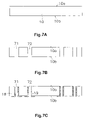
- FIGS. 7A , 7 B, and 7 C are cross-sectional views showing manufacturing steps of a semiconductor device.
- FIGS. 8A , 8 B, and 8 C are cross-sectional views showing manufacturing steps of a semiconductor device.
- FIGS. 9A and 9B are cross-sectional views showing manufacturing steps of a semiconductor device.
- FIG. 10 is an equivalent circuit of a semiconductor device in accordance with an alternative embodiment of the present invention.
- FIG. 1 shows a schematic cross-sectional view of a semiconductor device in accordance with an embodiment of the present invention.
- FIG. 2 shows a cross-sectional view of a cross section II-II of the semiconductor device shown in FIG. 1 .
- FIG. 3 shows a cross-sectional view of a cross section III-III of the semiconductor device shown in FIG. 1 .
- FIG. 4 shows an equivalent circuit of a semiconductor device. Note that a drawing of sealing resin filled in the spaces among the semiconductor substrates is omitted in FIG. 1 , and a circuit element is indicated with a dashed line in FIG. 3 .
- FIG. 1 Structural overview of a semiconductor device in accordance with an embodiment of the present invention will be hereinafter explained mainly with reference to FIG. 1 .
- a semiconductor device 1 is chiefly composed of a semiconductor substrate 10 , a capacitor chip 20 , a third semiconductor substrate 30 , a fourth semiconductor substrate 40 , an external input terminal 2 , an external output terminal 3 , a ground output terminal 4 , an interposer 5 , a first re-wiring 51 , and a second re-wiring 52 .
- the first semiconductor substrate 10 , the capacitor chip 20 , the third semiconductor substrate 30 , and the fourth semiconductor substrate 40 are laminated on the interposer 5 approximately parallel to each other.
- a circuit element (see a circuit element 16 shown in FIG. 3 ), an eleventh through-hole electrode 11 , a twelfth through-hole electrode 12 , a thirteenth through-hole electrode 13 , a fourteenth through-hole electrode 14 , a fifteenth through-hole electrode 15 , a seventeenth through-hole electrode 17 , and the like are formed in/on the first semiconductor substrate 10 .
- the eleventh through-hole electrode 11 , the twelfth through-hole electrode 12 , the thirteenth through-hole electrode 13 , and the seventeenth through-hole electrode 17 are formed to pass through the first semiconductor substrate 10 from the upper surface (i.e., top) to the lower surface (i.e., bottom). Because of this, the top and the bottom of the first semiconductor substrate 10 are configured to be able to communicate an electric signal.
- configurations of the third semiconductor substrate 30 and the fourth semiconductor substrate 40 are the same as the configuration of the first semiconductor substrate 10 .
- a capacitor element C 1 (see FIG. 5 ) to be described below is formed on the capacitor chip 20 .
- a simple element is formed on the capacitor chip 20 , compared to the first semiconductor substrate 10 , the third semiconductor substrate 30 , and the fourth semiconductor substrate 40 . Therefore, the area of the capacitor chip 20 is formed to be smaller than those of the first semiconductor substrate 10 , the third semiconductor substrate 30 , and the fourth semiconductor substrate 40 , while those of the first semiconductor substrate 10 , the third semiconductor substrate 30 , and the fourth semiconductor substrate 40 are approximately the same as each other.
- the capacitor chip 20 is located across the first semiconductor substrate 10 from the external input terminal 2 and the external output terminal 3 . In other words, it is laminated on the top of the laminated semiconductor substrates.
- the first re-wiring 51 is formed to extend horizontally so that it connects the capacitor chip 20 , and the eleventh through-hole electrode 11 and the twelfth through-hole electrode 12 .
- the second re-wiring 52 is formed to extend horizontally so that it connects the thirteenth through-hole electrode 13 and the capacitor chip 20 .
- the interposer 5 is chiefly composed of an insulating resin.
- a through-hole wiring 53 , a through-hole wiring 54 , and a through-hole wiring 55 , and the like are formed therein.
- the external input terminal 2 is coupled to the eleventh through-hole electrode 11 through the through-hole wiring 55 , a forty-first through-hole electrode 41 , and a thirty-first through-hole electrode 31 .
- the eleventh through-hole electrode 11 is coupled to the twelfth through-hole electrode 12 and the fourteenth through-hole electrode 14 through the first re-wiring 51 so that it branch off in two directions (See FIG. 3 ).
- the twelfth through-hole electrode 12 is connected to the input side of the circuit element 16 .
- the external output terminal 3 is coupled to the output side of the circuit element 16 through the seventeenth through-hole electrode 17 (see FIG. 3 ), a thirty-seventh through-hole electrode 37 , a forty-seventh through-hole electrode 47 , and the through-hole wiring 53 .
- the fourteenth through-hole electrode 14 is coupled to either of electrodes of the capacitor element C 1 formed on the capacitor chip 20 through a solder ball 24 (see FIG. 5 ).
- the ground output terminal 4 is coupled to the other electrode of the capacitor element C 1 through a solder ball 25 (see FIG. 5 ), the fifteenth through-hole electrode 15 , the second re-wiring 52 , the thirteenth through-hole electrode 13 , a thirty-third through-hole electrode 33 , a forty-third through-hole electrode 43 , and the through-hole wiring 54 .
- the ground output terminal 4 is coupled to the ground level.
- FIGS. 1 to 4 An operational overview of the semiconductor device in accordance with an embodiment of the present invention will be hereinafter explained with reference to FIGS. 1 to 4 .
- An externally input signal through the external input terminal 2 is transmitted to the first re-wiring 51 through the through-hole wiring 55 , the forty-first through-hole electrode 41 , the thirty-first through-hole electrode 31 , and the eleventh through-hole electrode 11 .
- high-frequency noise contained in a signal that is transmitted to the first re-wiring 51 will be allowed to escape to the ground level through the solder ball 24 , the capacitor element C 1 , the solder ball 25 , the thirteenth through-hole electrode 13 , the thirty-third through-hole electrode 33 , the forty-third through-hole electrode 43 , the through-hole wiring 54 , and the ground output terminal 4 .
- a signal that is transmitted to the first re-wiring 51 is input into the circuit element 16 through the twelfth through-hole electrode 12 in a state that the high-frequency noise is removed therefrom.
- a signal that is output from the circuit element 16 is externally output through the seventeenth through-hole electrode 17 , the thirty-seventh through-hole electrode 37 , the forty-seventh through-hole electrode 47 , the through-hole wiring 53 , and the external output terminal 3 .
- FIG. 5 shows an enlarged cross-sectional view of the capacitor chip. Note that the top and the bottom of the capacitor in FIG. 5 is shown to be turned upside down, compared to those of the capacitor shown in FIG. 1 .
- the capacitor chip 20 has a twenty-first surface 20 a and a twenty-second surface 20 b .
- the capacitor element C 1 , the solder ball 24 , the solder ball 25 , a metal post 26 , a metal post 27 , and a sealing resin 28 are chiefly formed on the twenty-first surface 20 a .
- the twenty-second surface 20 b is the surface of the capacitor chip 20 that is located opposite from the twenty-first surface 20 a.
- the capacitor element C 1 is formed to extend along the twenty-first surface 20 a .
- the capacitor element C 1 is chiefly composed of a first conductive layer 21 , a capacitor insulating layer 23 , and a second conductive layer 22 .
- the first conductive layer 21 chiefly consists of conductive material, and is formed on the entirety of the twenty-first surface 20 a .
- the capacitor insulating layer 23 chiefly consists of insulating material, and is formed to be located immediately above the first conductive layer 21 .
- the second conductive layer 22 chiefly consists of conductive material, and is formed to be located immediately above the capacitor insulating layer 23 .
- a protection film 29 is formed to cover the first conductive layer 21 , the capacitor insulating layer 23 , and the second conductive layer 22 .
- the first conductive layer 21 is formed to have the dimension of (55 ⁇ m) ⁇ (75 ⁇ m) and the thickness of approximately 100 ⁇ , for instance.
- the capacitor insulating layer 23 chiefly consists of insulating material (e.g., material of Ba—Sr—Ti—O system or Sr—Bi—Ta—O system) whose permittivity is larger than that of SiO 2 (e.g., permittivity is approximately 800), and is formed to have the dimension of (53 ⁇ m) ⁇ (60 ⁇ m) and the thickness of approximately 0.15 ⁇ m, for instance.
- the second conductive layer 22 is formed to have the dimension of (50 ⁇ m) ⁇ (50 ⁇ m) and the thickness of approximately 100 ⁇ , for instance.
- the capacitor element C 1 is configured to have capacitance (e.g., 2000 to 3000 pF) that is much larger than that of the capacitor element (normally approximately 0.1 to 1.5 pF) that is formed in a general semiconductor memory element. In other words, it is configured to be able to remove high-frequency noise from a sent/received signal.
- the solder ball 24 is coupled to the second conductive layer 22 through the metal post 26 .
- the solder ball 25 is coupled to the first conductive layer 21 through the metal post 27 .
- the sealing resin 28 is filled in a space between the metal post 26 and the metal post 27 . Because of this, it will be easier to electrically access the first conductive layer 21 and the second conductive layer 22 of the capacitor element C 1 separately.
- FIG. 6 shows an enlarged cross-sectional view of the first semiconductor substrate. Note that the top and the bottom of the semiconductor substrate in FIG. 6 is shown to be turned upside down, compared to those of the semiconductor substrate shown in FIG. 1 .
- the first semiconductor substrate 10 includes an eleventh surface 10 a , a twelfth surface 10 b , the eleventh through-hole electrode 11 , the twelfth through-hole electrode 12 , the thirteenth through-hole electrode 13 (see FIG. 1 ), and other members.
- the circuit element 16 , a protection film 62 , and a sealing resin 61 are chiefly formed on the eleventh surface 10 a .
- the twelfth surface 10 b is the surface of the first semiconductor substrate 10 that is located opposite from the eleventh surface 10 a .
- the protection film 63 is chiefly formed on the twelfth surface 10 b .
- the eleventh through-hole electrode 11 , the twelfth through-hole electrode 12 , the thirteenth through-hole electrode 13 , the seventeenth through-hole electrode 17 (see FIG. 1 ) and other members are formed to pass through the first semiconductor substrate 10 so that the eleventh surface 10 a side and the twelfth surface 10 b side are electrically connected to each other.
- the eleventh through-hole electrode 11 chiefly includes an upper electrode 11 a , a lower electrode 11 b , a through-hole wiring 11 c , an interconnecting electrode 11 h , an interconnecting wiring 11 i , a metal post 11 f , a solder ball 11 g , a backside wiring 11 d , and a land 11 e .
- the through-hole wiring 11 c is formed to pass through the semiconductor substrate 10 from the eleventh surface 10 a to the twelfth surface 10 b .
- the upper electrode 11 a and the lower electrode 11 b are electrically coupled to each other through the through-hole wiring 11 c .
- the solder ball 11 g is coupled to the upper electrode 11 a through the interconnecting wiring 11 i , the interconnecting electrode 11 h , the metal post 11 f .
- the land 11 e is coupled to the lower electrode 11 b through the backside wiring 11 d .
- the solder ball 11 g and the land 11 e are electrically coupled to each other.
- the twelfth through-hole electrode 12 chiefly includes an upper electrode 12 a , a lower electrode 12 b , a through-hole wiring 12 c , an interconnecting electrode 12 h , an interconnecting wiring 12 i , a metal post 12 f , a solder ball 12 g , a backside wiring 12 d , and a land 12 e .
- the through-hole wiring 12 c is formed to pass through the semiconductor substrate 10 from the eleventh surface 10 a to the twelfth surface 10 b .
- the upper electrode 12 a and the lower electrode 12 b are electrically coupled to each other through the through-hole wiring 12 c .
- the solder ball 12 g is coupled to the upper electrode 12 a through the metal post 12 f .
- the land 12 e is coupled to the lower electrode 12 b through the backside wiring 12 d .
- the solder ball 12 g and the land 12 e are electrically coupled to each other.
- a circuit element 16 chiefly includes an internal circuit 16 a and a connection wiring 16 b .
- the circuit element 16 is shown to have a single layer for a simplified explanation. However, the circuit element 16 is actually formed to have a more complex configuration. For example, an interlayer film may be formed in the circuit element 16 so that it is located to contact the first semiconductor substrate 10 .
- the eleventh through-hole electrode 11 and the twelfth through-hole electrode 12 are compared, they are different from each other in that the eleventh through-hole electrode 11 is electrically isolated from the circuit element 16 but the twelfth through-hole electrode 12 is electrically coupled to the circuit element 16 .
- the twelfth through-hole electrode 12 is different from the eleventh through-hole electrode 11 in that it is coupled to the internal circuit 16 a through the upper electrode 12 a and the connection wiring 16 b .
- a signal is configured to be provided to the circuit element 16 through the twelfth through-hole electrode 12 .
- the thirteenth through-hole electrode 13 and the seventeenth through-hole electrode 17 are compared, they are different from each other in that the thirteenth through-hole electrode 13 is electrically isolated from the circuit element 16 but the seventeenth through-hole electrode 17 is electrically coupled to the circuit element 16 .
- a signal is configured to be able to be output from the circuit element 16 to the external output terminal 3 through the seventeenth through-hole electrode 17 .
- the thirteenth electrode 13 (see FIGS. 4 and 5 ) that is electrically coupled to the first conductive layer 21 of the capacitor element C 1 on the capacitor chip 20 is electrically isolated from the circuit element 16 . Therefore, high-frequency noise is allowed to escape to the ground level without mixing into a signal in the circuit element 16 .
- a method configured to manufacture a semiconductor device will be hereinafter explained with reference to FIGS. 1 and 5 and cross-sectional views of manufacturing steps thereof shown in FIGS. 6 , 7 A to 7 C, 8 A to 8 C, and 9 A to 9 B.
- manufacturing methods of the eleventh through-hole electrode 11 and the twelfth through-hole electrode 12 will be hereinafter explained, and those of other through-hole electrodes (e.g., the thirteenth electrode 13 and the like) will be hereinafter omitted.
- the other through-hole electrodes are formed in the similar way used for forming the eleventh through-hole electrode 11 and the twelfth through-hole electrode 12 .
- a first semiconductor substrate is prepared in a preparation step S 1 .
- a first semiconductor substrate 10 includes an eleventh surface 10 a and a twelfth surface 10 b.
- an eleventh through-hole electrode 11 and a twelfth through-hole electrode 12 will be formed in a through-hole electrode formation step S 2 .
- through-holes 71 and 72 will be formed so that they pass through a protection film 62 and the first semiconductor substrate 10 in a direction from the eleventh surface 10 a to the twelfth surface 10 b in a region in which a circuit element 16 is not formed (see FIG. 6 ).
- FIG. 7B through-holes 71 and 72 will be formed so that they pass through a protection film 62 and the first semiconductor substrate 10 in a direction from the eleventh surface 10 a to the twelfth surface 10 b in a region in which a circuit element 16 is not formed (see FIG. 6 ).
- insulating layers 18 and 19 are formed to extend continuously from the inner sidewalls of the through holes 71 and 72 to the vicinity of the openings on the twelfth surface 10 b side. Then, as shown in FIG. 8A , through-hole wirings 11 c and 12 c will be formed by filling conductive material into the through holes 71 and 72 .
- a circuit element and upper electrodes will be formed on the eleventh surface of the first semiconductor substrate in an element formation step S 3 . More specifically, a circuit element 16 (i.e., an internal circuit 16 a and a connection wiring 16 b ) will be formed on the first surface 10 a of the first semiconductor substrate 10 by means of a photolithography step and the like. In addition, upper electrodes 11 a and 12 a will be formed on the eleventh through-hole electrode 11 and the twelfth through-hole electrode 12 , respectively.
- a circuit element 16 i.e., the internal circuit 16 a and the connection wiring 16 b
- the protection film 62 will be formed on the circuit element 16 , and the upper electrodes 11 a and 12 a.
- an interconnecting electrode and an interconnecting wiring will be formed in an interconnecting electrode formation step S 4 . More specifically, as shown in FIG. 9A , portions of the protection film 62 located immediately above the upper electrodes 11 a and 12 a will be removed, and openings 73 and 74 will be formed. Then, interconnecting wirings 11 i and 12 i will be formed by filling the openings 73 and 74 with conductive material. In addition, interconnecting electrodes 11 h and 12 h will be formed immediately above the interconnecting wirings 11 i and 11 i , respectively, by means of a photolithography step and the like.
- a lower electrode, a protection film, and a backside wiring will be formed on the twelfth surface of the first semiconductor substrate in a backside wiring formation step S 5 . More specifically, lower electrodes 11 b and 12 b will be formed immediately below the eleventh through-hole electrode 11 and the twelfth through-hole electrode 12 , respectively. Then, a protection film 63 will be formed to fill spaces including a space between the lower electrodes 11 b and 12 b . In addition, backside wirings 11 d and 12 d will be formed immediately below the lower electrodes 11 b and 12 b , respectively.
- resin seal will be performed to fill the first semiconductor substrate with a resin in a first resin sealing step S 6 . More specifically, as shown in FIG. 6 , metal posts 11 f and 12 f are formed, and a sealing resin 61 will be filled with a space between the metal posts 11 f and 12 f . Furthermore, solder balls 11 g and 12 g will be formed on the metal posts 11 f and 12 f , respectively. On the other hand, lands 11 e and 12 e will be formed immediately below the backside wirings 11 d and 12 d , respectively.
- a third semiconductor substrate 30 and a fourth semiconductor substrate 40 will be formed in steps that are similar to the steps S 1 to S 6 .
- the first semiconductor substrate, the third semiconductor substrate, and the fourth semiconductor substrate will be laminated in a first lamination step S 7 . More specifically, as shown in FIG. 1 , the third semiconductor substrate 30 will be laminated on the fourth semiconductor substrate 40 so that a solder ball 31 g of the third semiconductor substrate 30 contacts a land 41 e of the fourth semiconductor substrate 40 . Then, the first semiconductor substrate 10 will be laminated on the third semiconductor substrate 30 so that the solder ball 11 g of the first semiconductor substrate 10 contacts a land 31 e of the third semiconductor substrate 30 .
- a re-wiring layer will be formed on a land of the first semiconductor substrate in a re-wiring layer formation step S 8 . More specifically, as shown in FIG. 1 , a re-wiring layer 51 will be formed on the land 11 e of the first semiconductor substrate 10 so that the eleventh through-hole electrode 11 , the twelfth through-hole electrode 12 , and a fourteenth through-hole electrode 14 are coupled to each other (see FIG. 3 ). In addition, a re-wiring layer 52 will be formed on the land 17 e of the first semiconductor substrate 10 so that a fifteenth through-hole electrode 15 and a thirteenth through-hole electrode 13 are coupled to each other (see FIG. 3 ).
- a capacitor chip will be further laminated on the first semiconductor substrate in a second lamination step S 8 . More specifically, a capacitor chip 20 will be laminated on the first semiconductor substrate 10 so that a solder ball 24 formed on the capacitor chip 20 contacts a land 14 e of the fourteenth through-hole electrode 14 and a solder ball 25 contacts a land 15 e of the fifteenth through-hole electrode 15 (see FIG. 2 ).
- a sealing resin will be filled with the spaces among the capacitor chip, the first semiconductor substrate, the third semiconductor substrate, and the fourth semiconductor substrate in a second resin sealing step S 9 .
- the external input terminal 2 is herein electrically coupled to the capacitor element C 1 and the twelfth through-hole electrode 12 through the eleventh through-hole electrode 11 .
- the capacitor element C 1 is configured so that a signal is externally input therein through the first through-hole electrode 11 . Because of this, the degree-of-freedom of the electrode arrangement is increased, and the path length of a portion through which a signal is transmitted is reduced when a signal is transmitted to the capacitor element C 1 , compared to a case in which the external input terminal 2 is coupled to the capacitor element C 1 and the through-hole electrode 12 through a bonding wire.
- the degree-of-freedom of electrode arrangement is increased, and path length of a portion through which a signal is transmitted is reduced. Accordingly, the implementation area and transmission time for a signal will be reduced.
- the second conductive layer 22 of the capacitor element C 1 is herein coupled to the external input terminal 2 through the eleventh through-hole electrode 11 , and coupled to the circuit element 16 through the twelfth through-hole electrode 12 .
- the first conductive layer 21 is coupled to the ground level. Because of this, a signal that is externally input into the external input terminal 2 is configured to be input into the circuit element 16 in a state that high-frequency noise escapes to the ground level.
- the capacitor element C 1 is herein coupled to the external input terminal 2 through the eleventh through-hole electrode 11 and the thirty-first through-hole electrode 31 . Because of this, even if a plurality of semiconductor substrates on which a circuit element is formed are used, the degree-of-freedom of the electrode arrangement will be increased when a signal is transmitted to the capacitor element C 1 . Accordingly, the path length of a portion through which a signal is transmitted will be reduced.
- semiconductor substrates 10 , 30 , and 40 may be laminated in the semiconductor device.
- semiconductor substrates 10 , 30 , and 40 may be laminated in the semiconductor device.
- only one semiconductor substrate may be used in the semiconductor device.
- two semiconductor substrates may be laminated in the semiconductor device.
- the capacitor element C 1 may be formed with the wafer-level chip size package (WCSP) technique.
- WSP wafer-level chip size package
- the capacitor element C 1 may be coupled to the output side of the circuit element 16 instead of being coupled to the input side thereof.
- a semiconductor substrate 1 i includes a fourteenth through-hole electrode 14 i instead of including the above described fourteenth through-hole electrode 14 .
- the fourteenth through-hole electrode 14 i is coupled to the output side of the circuit element 16 and a seventeenth through-hole electrode 17 so that it branches off in two directions.
- the second conductive layer 22 of the capacitor element C 1 is configured to be coupled to the external output terminal 3 through the seventeenth through-hole electrode 17 . Because of this, a signal that is output from the circuit element 16 is configured to be able to be externally output from the external output terminal in a state that high-frequency noise escapes to the ground level.
- the equivalent circuit used in the semiconductor device may be formed by a combination of those shown in FIGS. 4 and 10 .
- the semiconductor device and the method configured to manufacture the same in accordance with the present invention are useful, in that they have an effect that transmission time for a signal is allowed to be reduced and implementation area is allowed to be reduced.
- a method for manufacturing a semiconductor device includes the steps of preparing a first semiconductor chip, forming a first circuit on the first surface of the semiconductor chip, forming a first through-hole electrode, a second through-hole electrode, and a third through-hole electrode, and laminating a capacitor chip on the first semiconductor chip.
- a step of preparing a first semiconductor chip a first semiconductor chip is prepared, and the first semiconductor chip includes a first surface and a second surface.
- the second surface is disposed on the opposite side of the first surface.
- a first circuit element is formed on the first surface of the first semiconductor chip.
- a first through-hole electrode, a second through-hole electrode, and a third through-hole electrode are formed.
- the first through-hole electrode penetrates the first semiconductor chip from the first surface to the second surface and is electrically isolated form the first circuit element.
- the second and third through-hole electrodes penetrate the first semiconductor chip from the first surface to the second surface and are electrically coupled to the first circuit element.
- a capacitor chip is laminated on the semiconductor chip.
- the capacitor chip includes a third surface, and a capacitor element is formed on the third surface. The capacitor element functions as a peripheral condenser component of the first semiconductor chip.
- a step of electrically coupling either of external input and output terminals to the capacitor element and second through-hole electrode and coupling the other of them to the first circuit element is performed at the same time as the step of laminating the capacitor chip on the first semiconductor chip.
- either the external input terminal or the external output terminal is electrically coupled to the capacitor element and the second through-hole electrode through the first through-hole electrode, and the other of the external input terminal and the external output terminal is coupled to the first circuit element through the third through-hole electrode.
- the external input terminal is disposed on the opposite side of the capacitor chip across the first semiconductor chip, and is configured such that a signal is externally input therein.
- the external output terminal is disposed on the opposite side of the capacitor chip across the first semiconductor chip, and is configured such that a signal is externally output therefrom.
- either the external input terminal or the external output terminal is allowed to be electrically coupled to the capacitor element and the second through-hole electrode through the first through-hole electrode at the same time as the step of laminating the capacitor chip on the first semiconductor chip.
- a signal is allowed to be externally input into the capacitor element through the first through-hole electrode.
- a signal is allowed to be output from the capacitor element through the first through-hole electrode.
- this enables the degree-of-freedom of the electrode arrangement to be increased, and enables the path length of a portion through which a signal is transmitted to be reduced when a signal is sent/received to/from the capacitor element, compared to a case in which either the external input terminal or the external output terminal is coupled to the capacitor element and the second through-hole electrode through a bonding wire.
- the degree-of-freedom of electrode arrangement is allowed to be increased, and the path length of a portion through which a signal is transmitted is allowed to be decreased. Therefore, implementation area and transmission time of a signal is allowed to be reduced.
- the term “configured” as used herein to describe a component, section or part of a device includes hardware and/or software that is constructed and/or programmed to carry out the desired function.
- the term “comprising” and its derivatives, as used herein are intended to be open ended terms that specify the presence of the stated features, elements, components, groups, integers, and/or steps, but do not exclude the presence of other unstated features, elements, components, groups, integers and/or steps.
- the foregoing also applied to words having similar meanings such as the terms, “including,” “having,” and their derivatives.
- the term “part,” “section,” “portion,” “member,” or “element” when used in the singular can have the dual meaning of a single part or a plurality of parts.
- terms of degree such as “substantially,” “about,” and “approximately” as used herein mean a reasonable amount of deviation of the modified term such that the end result is not significantly changed. For example, these terms can be construed as including a deviation of at least ⁇ 5% of the modified term if this deviation would not negate the meaning of the word it modifies.
Abstract
Description
Claims (3)
Applications Claiming Priority (2)
| Application Number | Priority Date | Filing Date | Title |
|---|---|---|---|
| JP2006-070286 | 2006-03-15 | ||
| JP2006070286A JP4714049B2 (en) | 2006-03-15 | 2006-03-15 | Semiconductor device and manufacturing method of semiconductor device |
Publications (2)
| Publication Number | Publication Date |
|---|---|
| US20070216020A1 US20070216020A1 (en) | 2007-09-20 |
| US7598618B2 true US7598618B2 (en) | 2009-10-06 |
Family
ID=38516955
Family Applications (1)
| Application Number | Title | Priority Date | Filing Date |
|---|---|---|---|
| US11/678,619 Active 2027-12-08 US7598618B2 (en) | 2006-03-15 | 2007-02-26 | Semiconductor device |
Country Status (2)
| Country | Link |
|---|---|
| US (1) | US7598618B2 (en) |
| JP (1) | JP4714049B2 (en) |
Cited By (10)
| Publication number | Priority date | Publication date | Assignee | Title |
|---|---|---|---|---|
| US20080303146A1 (en) * | 2007-06-07 | 2008-12-11 | Advanced Semiconductor Engineering, Inc. | Process for manufacturing substrate with bumps and substrate structure |
| US20090032969A1 (en) * | 2007-07-30 | 2009-02-05 | Camillo Pilla | Arrangement of Integrated Circuit Dice and Method for Fabricating Same |
| US20110062592A1 (en) * | 2009-09-11 | 2011-03-17 | Taiwan Semiconductor Manufacturing Company, Ltd. | Delamination Resistance of Stacked Dies in Die Saw |
| US20110278739A1 (en) * | 2010-05-11 | 2011-11-17 | Yi-Shao Lai | Semiconductor Package |
| US20120007251A1 (en) * | 2010-07-08 | 2012-01-12 | National Tsing Hua University | Stacked multi-chip |
| US20130214427A1 (en) * | 2012-02-16 | 2013-08-22 | Elpida Memory, Inc. | Semiconductor device having plural semiconductor chips stacked with each other |
| US9418876B2 (en) | 2011-09-02 | 2016-08-16 | Taiwan Semiconductor Manufacturing Company, Ltd. | Method of three dimensional integrated circuit assembly |
| US9859181B2 (en) | 2011-09-02 | 2018-01-02 | Taiwan Semiconductor Manufacturing Company, Ltd. | Underfill dispensing in 3D IC using metrology |
| US20190363042A1 (en) * | 2018-05-22 | 2019-11-28 | Murata Manufacturing Co., Ltd. | Semiconductor device |
| US10797030B2 (en) | 2017-06-19 | 2020-10-06 | Samsung Electronics Co., Ltd. | Semiconductor packages |
Families Citing this family (6)
| Publication number | Priority date | Publication date | Assignee | Title |
|---|---|---|---|---|
| JP5358089B2 (en) | 2007-12-21 | 2013-12-04 | スパンション エルエルシー | Semiconductor device |
| KR101465948B1 (en) * | 2007-12-27 | 2014-12-10 | 삼성전자주식회사 | A wafer level stack package and method of manufacturing a wafer level stack package |
| KR20100109241A (en) | 2009-03-31 | 2010-10-08 | 삼성전자주식회사 | Chip stack package and fabrication method thereof |
| US8710629B2 (en) * | 2009-12-17 | 2014-04-29 | Qualcomm Incorporated | Apparatus and method for controlling semiconductor die warpage |
| US9035194B2 (en) * | 2012-10-30 | 2015-05-19 | Intel Corporation | Circuit board with integrated passive devices |
| US20140167900A1 (en) | 2012-12-14 | 2014-06-19 | Gregorio R. Murtagian | Surface-mount inductor structures for forming one or more inductors with substrate traces |
Citations (3)
| Publication number | Priority date | Publication date | Assignee | Title |
|---|---|---|---|---|
| JPH113969A (en) | 1997-06-13 | 1999-01-06 | Matsushita Electric Ind Co Ltd | Substrate component laminated with chip component |
| US6914322B2 (en) * | 2001-12-26 | 2005-07-05 | Shinko Electric Industries Co., Ltd. | Semiconductor device package and method of production and semiconductor device of same |
| US20070126085A1 (en) * | 2005-12-02 | 2007-06-07 | Nec Electronics Corporation | Semiconductor device and method of manufacturing the same |
Family Cites Families (2)
| Publication number | Priority date | Publication date | Assignee | Title |
|---|---|---|---|---|
| JP2005340555A (en) * | 2004-05-28 | 2005-12-08 | Hitachi Ltd | Semiconductor integrated circuit element |
| JP4370993B2 (en) * | 2004-07-23 | 2009-11-25 | 日本電気株式会社 | Semiconductor device |
-
2006
- 2006-03-15 JP JP2006070286A patent/JP4714049B2/en active Active
-
2007
- 2007-02-26 US US11/678,619 patent/US7598618B2/en active Active
Patent Citations (3)
| Publication number | Priority date | Publication date | Assignee | Title |
|---|---|---|---|---|
| JPH113969A (en) | 1997-06-13 | 1999-01-06 | Matsushita Electric Ind Co Ltd | Substrate component laminated with chip component |
| US6914322B2 (en) * | 2001-12-26 | 2005-07-05 | Shinko Electric Industries Co., Ltd. | Semiconductor device package and method of production and semiconductor device of same |
| US20070126085A1 (en) * | 2005-12-02 | 2007-06-07 | Nec Electronics Corporation | Semiconductor device and method of manufacturing the same |
Cited By (16)
| Publication number | Priority date | Publication date | Assignee | Title |
|---|---|---|---|---|
| US7999380B2 (en) * | 2007-06-07 | 2011-08-16 | Advanced Semiconductor Engineering, Inc. | Process for manufacturing substrate with bumps and substrate structure |
| US20080303146A1 (en) * | 2007-06-07 | 2008-12-11 | Advanced Semiconductor Engineering, Inc. | Process for manufacturing substrate with bumps and substrate structure |
| US20090032969A1 (en) * | 2007-07-30 | 2009-02-05 | Camillo Pilla | Arrangement of Integrated Circuit Dice and Method for Fabricating Same |
| US7880309B2 (en) * | 2007-07-30 | 2011-02-01 | Qimonda Ag | Arrangement of stacked integrated circuit dice having a direct electrical connection |
| US20110062592A1 (en) * | 2009-09-11 | 2011-03-17 | Taiwan Semiconductor Manufacturing Company, Ltd. | Delamination Resistance of Stacked Dies in Die Saw |
| US8803332B2 (en) * | 2009-09-11 | 2014-08-12 | Taiwan Semiconductor Manufacturing Company, Ltd. | Delamination resistance of stacked dies in die saw |
| US20110278739A1 (en) * | 2010-05-11 | 2011-11-17 | Yi-Shao Lai | Semiconductor Package |
| US20120007251A1 (en) * | 2010-07-08 | 2012-01-12 | National Tsing Hua University | Stacked multi-chip |
| US8174126B2 (en) * | 2010-07-08 | 2012-05-08 | National Tsing Hua University | Stacked multi-chip |
| US9859181B2 (en) | 2011-09-02 | 2018-01-02 | Taiwan Semiconductor Manufacturing Company, Ltd. | Underfill dispensing in 3D IC using metrology |
| US9418876B2 (en) | 2011-09-02 | 2016-08-16 | Taiwan Semiconductor Manufacturing Company, Ltd. | Method of three dimensional integrated circuit assembly |
| US20130214427A1 (en) * | 2012-02-16 | 2013-08-22 | Elpida Memory, Inc. | Semiconductor device having plural semiconductor chips stacked with each other |
| US10797030B2 (en) | 2017-06-19 | 2020-10-06 | Samsung Electronics Co., Ltd. | Semiconductor packages |
| US11018121B2 (en) | 2017-06-19 | 2021-05-25 | Samsung Electronics Co., Ltd. | Semiconductor packages |
| US20190363042A1 (en) * | 2018-05-22 | 2019-11-28 | Murata Manufacturing Co., Ltd. | Semiconductor device |
| US11056423B2 (en) * | 2018-05-22 | 2021-07-06 | Murata Manufacturing Co., Ltd. | Semiconductor device |
Also Published As
| Publication number | Publication date |
|---|---|
| JP2007250708A (en) | 2007-09-27 |
| JP4714049B2 (en) | 2011-06-29 |
| US20070216020A1 (en) | 2007-09-20 |
Similar Documents
| Publication | Publication Date | Title |
|---|---|---|
| US7598618B2 (en) | Semiconductor device | |
| KR100535181B1 (en) | Semiconductor chip package having decoupling capacitor and manufacturing method thereof | |
| JP4917225B2 (en) | Semiconductor device | |
| US7884458B2 (en) | Decoupling capacitor, wafer stack package including the decoupling capacitor, and method of fabricating the wafer stack package | |
| US6891248B2 (en) | Semiconductor component with on board capacitor | |
| US6061228A (en) | Multi-chip module having an integral capacitor element | |
| US8178975B2 (en) | Semiconductor package with pad parts electrically connected to bonding pads through re-distribution layers | |
| US20090032973A1 (en) | Semiconductor stack package having wiring extension part which has hole for wiring | |
| JPS6355213B2 (en) | ||
| JP2002305283A (en) | Three-dimensional multichip package and method of manufacturing the same | |
| EP1280203A2 (en) | 3D-Semiconductor Package | |
| US8520402B1 (en) | Decoupling capacitor circuit assembly | |
| JP2009141169A (en) | Semiconductor device | |
| US6528871B1 (en) | Structure and method for mounting semiconductor devices | |
| US20120083096A1 (en) | Semiconductor device having a simplified stack and method for manufacturing tehreof | |
| TW201802946A (en) | Semiconductor device | |
| JP2000124015A (en) | Low-crosstalk ball grid array resistor circuit network | |
| US20090250801A1 (en) | Semiconductor device | |
| US20020100949A1 (en) | Bonding pad structure of semiconductor device and method for fabricating the same | |
| JP7015691B2 (en) | Semiconductor device | |
| KR101696705B1 (en) | Chip embedded type printed circuit board and method of manufacturing the same and stack package using the same | |
| JP2010206021A (en) | Electronic component mounting structure and method of manufacturing the same | |
| US8546186B2 (en) | Planar interconnect structure for hybrid circuits | |
| KR102508909B1 (en) | Semiconductor device and method for manufacturing same | |
| KR100818116B1 (en) | Semiconductor package |
Legal Events
| Date | Code | Title | Description |
|---|---|---|---|
| AS | Assignment |
Owner name: OKI ELECTRIC INDUSTRY CO., LTD., JAPAN Free format text: ASSIGNMENT OF ASSIGNORS INTEREST;ASSIGNOR:SHIRAISHI, YASUSHI;REEL/FRAME:018938/0758 Effective date: 20070222 |
|
| AS | Assignment |
Owner name: OKI SEMICONDUCTOR CO., LTD., JAPAN Free format text: CHANGE OF NAME;ASSIGNOR:OKI ELECTRIC INDUSTRY CO., LTD.;REEL/FRAME:022162/0586 Effective date: 20081001 Owner name: OKI SEMICONDUCTOR CO., LTD.,JAPAN Free format text: CHANGE OF NAME;ASSIGNOR:OKI ELECTRIC INDUSTRY CO., LTD.;REEL/FRAME:022162/0586 Effective date: 20081001 |
|
| STCF | Information on status: patent grant |
Free format text: PATENTED CASE |
|
| FPAY | Fee payment |
Year of fee payment: 4 |
|
| AS | Assignment |
Owner name: LAPIS SEMICONDUCTOR CO., LTD., JAPAN Free format text: CHANGE OF NAME;ASSIGNOR:OKI SEMICONDUCTOR CO., LTD;REEL/FRAME:032495/0483 Effective date: 20111003 |
|
| FPAY | Fee payment |
Year of fee payment: 8 |
|
| MAFP | Maintenance fee payment |
Free format text: PAYMENT OF MAINTENANCE FEE, 12TH YEAR, LARGE ENTITY (ORIGINAL EVENT CODE: M1553); ENTITY STATUS OF PATENT OWNER: LARGE ENTITY Year of fee payment: 12 |
|
| AS | Assignment |
Owner name: ACHLYS TECHNOLOGIES INC., CANADA Free format text: ASSIGNMENT OF ASSIGNORS INTEREST;ASSIGNOR:LAPIS SEMICONDUCTOR CO., LTD.;REEL/FRAME:059559/0280 Effective date: 20220311 |
|
| AS | Assignment |
Owner name: TAIWAN SEMICONDUCTOR MANUFACTURING COMPANY, LTD., TAIWAN Free format text: ASSIGNMENT OF ASSIGNORS INTEREST;ASSIGNOR:ACHLYS TECHNOLOGIES INC.;REEL/FRAME:060244/0398 Effective date: 20220414 |