US7522156B2 - Optical scanning-type touch panel - Google Patents
Optical scanning-type touch panel Download PDFInfo
- Publication number
- US7522156B2 US7522156B2 US09/875,084 US87508401A US7522156B2 US 7522156 B2 US7522156 B2 US 7522156B2 US 87508401 A US87508401 A US 87508401A US 7522156 B2 US7522156 B2 US 7522156B2
- Authority
- US
- United States
- Prior art keywords
- scanning
- light
- unit
- optical
- light receiving
- Prior art date
- Legal status (The legal status is an assumption and is not a legal conclusion. Google has not performed a legal analysis and makes no representation as to the accuracy of the status listed.)
- Expired - Fee Related, expires
Links
Images


Classifications
-
- G—PHYSICS
- G06—COMPUTING; CALCULATING OR COUNTING
- G06F—ELECTRIC DIGITAL DATA PROCESSING
- G06F3/00—Input arrangements for transferring data to be processed into a form capable of being handled by the computer; Output arrangements for transferring data from processing unit to output unit, e.g. interface arrangements
- G06F3/01—Input arrangements or combined input and output arrangements for interaction between user and computer
- G06F3/03—Arrangements for converting the position or the displacement of a member into a coded form
- G06F3/041—Digitisers, e.g. for touch screens or touch pads, characterised by the transducing means
- G06F3/042—Digitisers, e.g. for touch screens or touch pads, characterised by the transducing means by opto-electronic means
- G06F3/0421—Digitisers, e.g. for touch screens or touch pads, characterised by the transducing means by opto-electronic means by interrupting or reflecting a light beam, e.g. optical touch-screen
- G06F3/0423—Digitisers, e.g. for touch screens or touch pads, characterised by the transducing means by opto-electronic means by interrupting or reflecting a light beam, e.g. optical touch-screen using sweeping light beams, e.g. using rotating or vibrating mirror
Definitions
- the display region has a rectangular shape
- the diagonal section is the farthest point for scanning light and has a large incident angle
- the level of the light receiving signal becomes lower at the diagonal section.
- the S/N ratio is impaired, causing a malfunction.
- FIG. 16 is a graph showing the relationship between the film thickness of a protective film of the polygon mirror and the reflectance
- FIG. 19 is a schematic diagram showing an indicator and a cut-off range
- FIG. 20 is a timing chart showing the relationship between the light receiving signal and the scanning angle and scanning time.
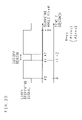
- FIG. 1 is a schematic diagram showing the basic structure of an optical scanning-type touch panel of the present invention.
- Optical units 1 a and 1 b having therein an optical system composed of a light emitting element, a light receiving element, a polygon mirror and various lenses are respectively provided on the outside of both corners of one short side (the right side in this embodiment) of this rectangular display screen 10 that is the extent of a plane specified as a target area to be touched by an indicator S such as a finger and pen.
- a recurrence reflection sheet 7 as a retro-reflector is provided on the outside of three sides other than the right side of the display screen 10 , namely, the upper, lower and left sides.
- This structure secures the aperture mirror 15 with a light receiving surface height as high as the height of the light receiving surface of the polygon mirror 14 , and it is meaningless to make the aperture mirror 15 larger than this level because even if the aperture mirror 15 is made larger than this level, only a region which does not contribute to the reception of light increases.
- the aperture mirror 15 By designing the aperture mirror 15 to have such a structure, it is possible to improve the light receiving efficiency in comparison with a structure having a light receiving surface symmetrical in the vertical direction, without changing the scanning surface height.
- FIG. 8 is a graph showing the relationship between the scanning angle and the light receiving scanning surface opening width. Since the beam width is finite, the light receiving surface on the scanning region side must not extend into a detection region. The S/N ratio is most lowered when scanning the diagonal section (when the scanning angle is 66 degrees) at which the quantity of the reflected light is minimum, and, therefore, in the present invention, in order to secure a light receiving scanning surface opening width (w+W) for this scanning, the width of the aperture mirror 15 is specified to this light receiving scanning surface opening width (w+W). Moreover, in the present invention, the polygon mirror 14 is set at a mountable maximum height, and the height of the aperture mirror 15 is determined in accordance with the height of the polygon mirror 14 .
- FIG. 13 is a graph showing the reflectance characteristic of this cold mirror coat and the transmittance characteristic of this visible light cut-off filter, and it will be understood from FIG. 13 that only light in the vicinity of 780 nm can be selectively reflected. Further, it is also possible to perform a similar function by combining a hot mirror coat and an infrared light cut-off filter.
- the beam width of the scanning light is denoted by d
- the following condition (1) it is possible to receive the reflected light of the scanning light from the recurrence reflection sheet 7 by the light receiving elements 13 without being cut-off by the optical units 1 a and 1 b .
- the positions of the respective optical members are designed to satisfy this condition (1).
- ⁇ 00 and ⁇ 00 represent the angles from the scanning reference line to the respective light receiving elements
- ⁇ 0 and ⁇ 0 represent the angles from the scanning reference line to the ends of the recurrence reflection sheet 7
- ⁇ 1 and ⁇ 1 represent the angles from the scanning reference line to one end of the indicator S on the reference line side
- ⁇ 2 and ⁇ 2 represent the angles from the scanning reference line to another end of the indicator S on the opposite side to the reference side, respectively.
- FIG. 20 is a timing chart showing the relationship between the light receiving signal from the light receiving signal detector 3 a and the scanning angle ⁇ and scanning time T of the polygon mirror 14 in the optical unit 1 a .
- the scanning angular velocity of the polygon mirror 14 is constant, if the scanning angular velocity is represented by ⁇ , a proportional relationship as shown by equation (6) below is established between the scanning angle ⁇ and the scanning time T.
- ⁇ ⁇ T (6)
- any optical member having the light transmitting and light reflecting functions may be used, and, it is possible to use a half mirror, beam splitter, etc., for example.
- the height of the deflecting unit is arranged to be the same as the height of the optical scanning unit, it is possible to eliminate an unnecessary light receiving surface from the deflecting unit and prevent reception of disturbing light, thereby achieving a high S/N ratio.
Abstract
Laser light emitted by a light emitting element is made parallel light by a collimation lens, passes through an aperture of an aperture mirror, and is then angularly scanned in a plane substantially parallel to a display screen by rotation of a polygon mirror and projected onto a recurrence reflection sheet. Then, after the reflected light from the recurrence reflection sheet is reflected by the polygon mirror and aperture mirror, the light is focused by a condenser lens to enter a light receiving element. The aperture mirror has an asymmetrical shape in the scanning direction and/or the vertical direction about the optical axis, according to a scanning surface opening width of the polygon mirror.
Description
This application is a continuation of international application PCT/JP99/06809 filed Dec. 3, 1999.
The present invention relates to an optical scanning-type touch panel for optically detecting the position of an indicator on a display screen.
With the spread of computer systems, mainly personal computers, there has been used a device for inputting new information or giving various instructions to a computer system by pointing at a position on a display screen of a display device on which information is displayed by the computer system, with a person's finger or a specific indicator.
In order to perform an input operation with respect to the information displayed on the display screen of the display device of a personal computer or the like by a touching method, it is necessary to detect a touched position (indicated position) on the display screen with high accuracy. As one example of such a method of detecting the indicated position on the display screen serving as a coordinate surface, Japanese Patent Application Laid-Open No. 62-5428/1987 discloses an optical position detecting method. In this method, a light retro-reflector is positioned on a frame on both sides of the display screen, return light of an angularly scanned laser beam from the light retro-reflector is detected, an angle of a position where a finger or pen exists is calculated from a timing that the light beam is cut off by the finger or pen, and the coordinate of the position is detected from the calculated angle according to the triangulation principle. In this method, the accuracy of detection can be maintained with a small number of parts, and the position of the finger, arbitrary pen or the like is also detectable.
An optical scanning-type touch panel for performing such a position detection by scanning light is constructed by a retro-reflector which is generally positioned on the outside of the display screen, a light emitting element for emitting light such as laser light, an optical scanning unit such as a polygon mirror for angularly scanning the emitted light, a deflecting element for deflecting the reflected light of the scanning light from the retro-reflector, and a light receiving element for receiving the deflected reflected light so that the light from the light emitting element is scanned by the optical scanning unit, the reflected light of the scanning light from the retro-reflector is reflected again by the optical scanning unit, and the resultant reflected light is received by the light receiving element through the deflecting element. When an indicator, such as a pen and arbitrary pen, is present on the path of the scanning light, the light reflected by the retro-reflector is not received by the light receiving element. It is therefore possible to detect the position of such an indicator based on the scanning angle of the optical scanning unit and the light receiving result at the light receiving element.
In such an optical scanning-type touch panel, in general, the larger the incident angle on the retro-reflector becomes, the lower the efficiency of retro-reflection becomes, and the longer the distance from the optical scanning unit to the retro-reflector becomes, the lower the luminance becomes because the reflected light from the retro-reflector is wider due to the diffraction effect of the beam. Hence, in the case where the display region has a rectangular shape, since the diagonal section is the farthest point for scanning light and has a large incident angle, the level of the light receiving signal becomes lower at the diagonal section. As a result, the S/N ratio is impaired, causing a malfunction. In addition, it is also important to take some measures against disturbing light that impairs the S/N ratio.
The present invention was invented in view of such circumstances, and an object of the present invention is to provide an optical scanning-type touch panel capable of achieving a high S/N ratio by increasing the level of the light receiving signal and thereby accurately detecting the position of the indicator.
An optical scanning-type touch panel of the first invention comprising: an optical scanning unit for angularly scanning light in a plane substantially parallel to a predetermined region; a deflecting unit for deflecting scanning light of the optical scanning unit; and a light receiving unit for receiving the deflected scanning light, for detecting a scanning light cut-off position, which is produced in the predetermined region by an indicator, based on a light receiving output of the light receiving unit that corresponds to a scanning angle, wherein the deflecting unit has an asymmetrical shape about an optical axis. In the optical scanning-type touch panel of the first invention, the deflecting unit is formed in an asymmetrical shape about the optical axis so as to enlarge the effective light receiving area for the scanning light and improve the light receiving signal level.
In an optical scanning-type touch panel of the second invention according to the first invention, the shape of the deflecting unit is asymmetrical in the scanning direction. In the optical scanning-type touch panel of the second invention, the shape of the deflecting unit is made asymmetrical in the scanning direction so as to enlarge the effective light receiving area for the scanning light and improve the light receiving signal level.
In an optical scanning-type touch panel of the third invention according to the first invention, the shape of the deflecting unit is asymmetrical in the height direction. In the optical scanning-type touch panel of the third invention, the shape of the deflecting unit is made asymmetrical in the height direction so as to enlarge the effective light receiving area for the scanning light and improve the light receiving signal level.
In an optical scanning-type touch panel of the fourth invention according to the third invention, the height of the deflecting unit is substantially equal to the height of the optical scanning unit. In the optical scanning-type touch panel of the fourth invention, the height of the deflecting unit is made substantially equal to the height of the optical scanning unit so as to eliminate an unnecessary light receiving surface from the deflecting unit and prevent reception of disturbing light.
In an optical scanning-type touch panel of the fifth invention according to the fourth invention, the predetermined region has a rectangular shape, and the width of the deflecting unit is substantially equal to a scanning surface opening width of the optical scanning unit in scanning a diagonal section of the predetermined region with light. In the optical scanning-type touch panel of the fifth invention, the width of the deflecting unit is made substantially equal to the scanning surface opening width of the optical scanning unit in scanning the diagonal section of the predetermined region with light so as to eliminate an unnecessary light receiving surface from the deflecting unit and prevent reception of disturbing light.
An optical scanning-type touch panel of the sixth invention comprising: an optical scanning unit for angularly scanning light in a plane substantially parallel to a predetermined region; a deflecting unit for deflecting scanning light of the optical scanning unit; and a light receiving unit for receiving the deflected scanning light, for detecting a scanning light cut-off position, which is produced in the predetermined region by an indicator, based on a light receiving output of the light receiving unit that corresponds to a scanning angle, wherein the optical scanning-type touch panel satisfies a condition
d/2+w<D tan δ
where D is a distance from the optical scanning unit to the deflecting unit, w is a width on the deflecting unit from a path of the scanning light to an end on the predetermined region side, d is a beam width of the scanning light, and δ is a scanning start angle.
d/2+w<D tan δ
where D is a distance from the optical scanning unit to the deflecting unit, w is a width on the deflecting unit from a path of the scanning light to an end on the predetermined region side, d is a beam width of the scanning light, and δ is a scanning start angle.
In the optical scanning-type touch panel of the sixth invention, it is possible to certainly scan light within the predetermined region by satisfying the relationship as described above.
An optical scanning-type touch panel of the seventh invention comprising: a light retro-reflector provided outside of a predetermined region; an optical scanning unit for angularly scanning light in a plane substantially parallel to the predetermined region; and a light receiving unit for receiving reflected light of scanning light of the optical scanning unit from the light retro-reflector, for detecting a scanning light cut-off position, which is produced in the predetermined region by an indicator, based on a light receiving output of the light receiving unit that corresponds to a scanning angle, wherein the optical scanning unit is provided with a protective film having a maximum reflectance at an angle of incidence corresponding to a scanning angle at which the quantity of the reflected light is minimum. In the optical scanning-type touch panel of the seventh invention, the optical scanning unit is provided with the protective film having the maximum reflectance at an angle of incidence corresponding to a scanning angle at which the quantity of the reflected light is minimum so as to improve the light receiving signal level in scanning the position at which the quantity of the reflected light is minimum with light.
The following description will explain the present invention in detail with reference to the drawings illustrating an embodiment thereof. FIG. 1 is a schematic diagram showing the basic structure of an optical scanning-type touch panel of the present invention.
In FIG. 1 , reference numeral 10 is a rectangular display screen of a CRT, flat display panel (PDP, LCD, EL, etc.) or projection-type image display device of electronic equipment such as a personal computer, and the optical scanning-type touch panel is constructed as the display screen of a PDP (Plasma Display Panel) in this embodiment.
Optical units 1 a and 1 b having therein an optical system composed of a light emitting element, a light receiving element, a polygon mirror and various lenses are respectively provided on the outside of both corners of one short side (the right side in this embodiment) of this rectangular display screen 10 that is the extent of a plane specified as a target area to be touched by an indicator S such as a finger and pen. Moreover, a recurrence reflection sheet 7 as a retro-reflector is provided on the outside of three sides other than the right side of the display screen 10, namely, the upper, lower and left sides.
The laser light emitted by the light emitting element 11 is made parallel light by the collimation lens 12, passes through the aperture 15 a of the aperture mirror 15, and is then angularly scanned in a plane substantially parallel with the display screen 10 by rotation of the polygon mirror 14 and projected onto the recurrence reflection sheet 7. After the reflected light from the recurrence reflection sheet 7 is reflected by the polygon mirror 14 and aperture mirror 15, the reflected light is focused by the condenser lens 16 to enter the light receiving element 13. However, if the indicator S is present on the optical path of the scanning light, the scanning light is cut off, and therefore the reflected light does not enter the light receiving element 13.
The optical units 1 a and 1 b are connected with light emitting element drivers 2 a and 2 b for driving the respective light emitting elements 11, light receiving signal detectors 3 a and 3 b for converting the quantity of light received by the respective light receiving elements 13 into electric signals, and a polygon controller 4 for controlling the operation of the respective polygon mirrors 14. Moreover, reference numeral 5 represents an MPU for calculating the position and size of the indicator S and for controlling the operation of the entire apparatus, and 6 represents a display device for displaying the results of calculations performed by the MPU 5.
The MPU 5 transmits drive control signals to the light emitting element drivers 2 a and 2 b, so that the light emitting element drivers 2 a and 2 b are driven according to the drive control signals and the light emitting operations of the respective light emitting elements 11 are controlled. The light receiving signal detectors 3 a and 3 b transmit the light receiving signals of the reflected light of the respective light receiving elements 13 to the MPU 5. The MPU 5 calculates the position and size of the indicator S based on the light receiving signals from the respective light receiving elements 13, and displays the results of the calculations on the display device 6. Here, the display device 6 may also serve as the display screen 10.
In such an optical scanning-type touch panel of the present invention, if the explanation is given with respect to the optical unit 1 b, for example, as shown in FIG. 1 , the projected light from the optical unit 1 b is scanned in a counterclockwise direction in FIG. 1 from a position where the projected light is reflected by the aperture mirror 15 and directly enters the light receiving element 13 to a position (Ps) where the projected light is reflected by an end of the recurrence reflection sheet 7, that is, a scanning start position. Then, the projected light is reflected by the recurrence reflection sheet 7 until it comes to a position (P1) where the projected light reaches one end of the indicator S, but the projected light is cut off by the indicator S up to a position (P2) where it reaches the other end of the indicator S, and then the projected light is reflected by the recurrence reflection sheet 7 until it comes to a scanning end position (Pe).
In such scanning of light, a detected light signal given when the projected light from the light emitting element 11 directly enters the light receiving element 13 from the polygon mirror 14 through the aperture mirror 15 without reaching the recurrence reflection sheet 7 is used as a reference signal. Moreover, a detected light signal given when the scanning light reaches the end (PS in FIG. 1 ) of the recurrence reflection sheet 7 and is reflected therefrom serves as a scanning start signal, and then a recurrence reflection signal is obtained when the reflected light from the recurrence reflection sheet 7 enters the light receiving element 13. Besides, the scanning angle is measured upon the detection of this reference signal.
At this time, the reflected light B becomes wider in comparison with the scanning light A. FIG. 4 is an illustration showing the profiles of the scanning light A and reflected light B cut along the C-C line in the scanning region of FIG. 3 . In comparison with the scanning light A having a diameter of around 1 mm with the optical axis at its center, the reflected light B has a larger diameter of around 30 mm with the optical axis at its center.
Therefore, when a noise level is specified, an increase of the light receiving area, that is, the effective light receiving area of the aperture mirror 15, contributes to an improvement of the S/N ratio. However, it is not preferable to increase the aperture mirror 15 boundlessly, and the aperture mirror 15 should be fabricated in a small size in view of an improvement of the degree of freedom of the mount design. For this reason, it is necessary to design the polygon mirror 14 and aperture mirror 15 in optimum sizes. In particular, the effective light receiving area of the polygon mirror 14 varies according to a scanning angle in scanning. Moreover, since the light receiving signal level in scanning the farthest point within the scanning region determines the lowest level, it is desirable to design the aperture mirror 15 and polygon mirror 14 so that a cross-sectional area of the polygon mirror 14 seen from the aperture mirror 15 and a cross-sectional area of the aperture mirror 15 seen from an optical axis direction in scanning the farthest point are identical with each other, and it is possible to construct an optimum scanning light receiving system in such a design.
By the way, since the display screen 10 is located below the path of the scanning light, even when the lower side of the light receiving surface of the aperture mirror 15 is enlarged, it does not contribute to an improvement of the light receiving efficiency. It is therefore preferable to secure a large light receiving area on the side higher than the scanning surface of the polygon mirror 14 by designing the shape of the aperture mirror 15 asymmetrical in the vertical direction about the optical axis. FIG. 6 is a front view of the aperture mirror 15 designed accordingly, and FIG. 7 is a schematic diagram of a scanning light receiving system of the present invention using such an aperture mirror 15.
This structure secures the aperture mirror 15 with a light receiving surface height as high as the height of the light receiving surface of the polygon mirror 14, and it is meaningless to make the aperture mirror 15 larger than this level because even if the aperture mirror 15 is made larger than this level, only a region which does not contribute to the reception of light increases. By designing the aperture mirror 15 to have such a structure, it is possible to improve the light receiving efficiency in comparison with a structure having a light receiving surface symmetrical in the vertical direction, without changing the scanning surface height.
The aperture mirror 15 is made of a metal such as aluminum, but, when its surface rusts, its reflectance characteristic deteriorates. In the present invention, therefore, a surface of the aperture mirror 15 that faces the polygon mirror 14 has a mirror finish, and the mirror-finished surface is covered with a protective film 15 b made of a dielectric such as SiO and SiO2 for protecting the mirror-finished surface from moisture and dust which cause rust. Besides, in this example, the angle of incidence of the reflected light from the recurrence reflection sheet 7 on the aperture mirror 15 (protective film 15 b) is 45 degrees.
Moreover, it is possible to provide on the surface of the aperture mirror 15 an antireflection film having a multi-layer film structure for preventing reflection of light other than the scanning light of a specific wavelength (780 nm). FIG. 12 is a graph showing the wavelength-reflectance characteristics of this antireflection film when the angle of incidence is 45 degrees, and this antireflection film has a characteristic of selectively reflecting light in the vicinity of 780 nm. Thus, since a high reflectance characteristic can be exhibited only for the specific angle of incidence (45 degrees) and wavelength (780 nm) of incident light by providing such an antireflection film, it is possible to guide only desired recurrence reflected light to the light receiving system and prevent reflection of disturbing light, thereby improving the S/N ratio.
Furthermore, by combining a cold mirror coat for efficiently removing infrared ray components and a visible light cut-off filter and appropriately using the band difference therebetween, it is possible to perform a function of selectively reflecting the recurrence reflected light of the specific wavelength (780 nm). FIG. 13 is a graph showing the reflectance characteristic of this cold mirror coat and the transmittance characteristic of this visible light cut-off filter, and it will be understood from FIG. 13 that only light in the vicinity of 780 nm can be selectively reflected. Further, it is also possible to perform a similar function by combining a hot mirror coat and an infrared light cut-off filter.
Next, the following description will explain an arrangement of the optical units 1 a and 1 b in the optical scanning-type touch panel of the present invention. FIG. 14 is a schematic diagram showing the positional design of the optical members of the optical units 1 a and 1 b and a state of scanning light.
In FIG. 14 , δ represents a scanning start angle (the angle formed by the optical axis of parallel light from the aperture 15 a and the optical path of scanning light corresponding to Ps in FIG. 1 that actually strikes the recurrence reflection sheet 7), and the scanning start angle δ is expressed by the sum of an angle α formed by a scanning reference line (the line connecting both the optical units 1 a and 1 b) and the optical axis of parallel light from the aperture 15 a (i.e., the angle of tilting the optical unit 1 a, 1 b from the scanning reference line toward a non-scanning region side (non-detection region side) and an angle β formed by the scanning reference line and the optical path of the scanning light corresponding to Ps. Besides, D represents the distance from the aperture mirror 15 to the polygon mirror 14, w is a width on the aperture mirror 15 from the optical path of the scanning light to an end on the scanning region side (detection region side), and W is a width on the aperture mirror 15 from the optical path of the scanning light to an end on the non-scanning region side (non-detection region side).
Here, when the beam width of the scanning light is denoted by d, if the following condition (1) is further satisfied, it is possible to receive the reflected light of the scanning light from the recurrence reflection sheet 7 by the light receiving elements 13 without being cut-off by the optical units 1 a and 1 b. Hence, the positions of the respective optical members are designed to satisfy this condition (1).
d/2+w<D tan δ (1)
d/2+w<D tan δ (1)
By adopting such design specifications, it is possible to eliminate unnecessary space for mounting, scan light within the scanning range and receive the reflected light, and receive only the recurrence reflected light even at the start of scanning. Further, an example of specific numerical values is, for instance, α=6 degrees, β=3 degrees, δ=9 degrees, w+W=7 mm, d=3 mm, and D=45 mm. In this case, the aperture mirror 15 may have an asymmetrical shape (w≠W) or a symmetrical shape (w=W).
By the way, as described above, in order to secure the minimum quantity of light in scanning the diagonal section (the direction of 60 degrees from the scanning reference line) within the scanning region, when the polygon mirror 14 with four faces is used, since the angle of incidence is 33 degrees (the scanning angle is 66 degrees) for a scanning start angle δ of 6 degrees, it is possible to secure an effective light receiving area of cos 33° of the face width of the polygon mirror 14. Accordingly, when the face width of the polygon mirror 14 is 11 mm, the width (w+W) of the aperture mirror 15 is given by 11×cos 33°=9.23 mm.
Like the above-described aperture mirror 15, when the surface of the polygon mirror 14 rusts, the reflectance characteristic is impaired. In the present invention, therefore, as shown in FIG. 15 , the surface of the polygon mirror 14 is covered with a protective film 14 a made of a dielectric such as SiO and SiO2 for protecting the mirror-finished surface from moisture and dust which cause rust.
Next, the following description will explain an operation of calculating the position and size of the indicator S by the optical scanning-type touch panel of the present invention. FIG. 17 is a schematic diagram showing a state of implementation of the optical scanning-type touch panel. In FIG. 17 , however, illustration of the constituent members other than the optical units 1 a, 1 b, recurrence reflection sheet 7 and display screen 10 is omitted. Incidentally, FIG. 17 shows an example in which a finger is used as the indicator S.
The MPU 5 controls the polygon controller 4 to rotate the respective polygon mirrors 14 in the optical units 1 a and 1 b, thereby angularly scanning the laser light from the respective light emitting elements 11. As a result, the reflected light from the recurrence reflection sheet 7 enters the respective light receiving elements 13. The quantity of the received light that entered the respective light receiving elements 13 as mentioned above is obtained as the light receiving signals which are the outputs of light receiving signal detectors 3 a and 3 b.
Further, in FIG. 17 , θ00 and φ00 represent the angles from the scanning reference line to the respective light receiving elements, θ0 and φ0 represent the angles from the scanning reference line to the ends of the recurrence reflection sheet 7, θ1 and φ1 represent the angles from the scanning reference line to one end of the indicator S on the reference line side, and θ2 and φ2 represent the angles from the scanning reference line to another end of the indicator S on the opposite side to the reference side, respectively. Here, θ00 or φ00 correspond to the above-mentioned angle α; θ0 or φ0 correspond to the above-mentioned angle β; and (θ00+θ0) or (φ00+φ0) correspond to the above-mentioned scanning start angle δ.
When the indicator S is present on the optical path of the scanning light on the display screen 10, the light projected from the optical units 1 a and 1 b and then reflected by the indicator S does not enter the respective light receiving elements 13. Therefore, in a state as shown in FIG. 17 , the reflected light does not enter the light receiving element 13 in the optical unit 1 a when the scanning angle is in a range between 0° and θ0, the reflected light enters that light receiving element 13 when the scanning angle is in a range between θ0 and θ1, and the reflected light does not enter that light receiving element 13 when the scanning angle is in a range between θ1 and θ2. Similarly, the reflected light does not enter the light receiving element 13 in the optical unit 1 b when the scanning angle is in a range between 0° and φ0, the reflected light enters that light receiving element 13 when the scanning angle is in a range between φ0 and φ1, and the reflected light does not enter that light receiving element 13 when the scanning angle is in a range between φ1 and φ2,
Next, the following description will explain a process of calculating a coordinate of a central position (indicated position) of the indicator S (a finger in this example) from the cut-off range calculated in the above-mentioned manner. First, conversion of an angle into an orthogonal coordinate based on the triangulation will be explained. As shown in FIG. 18 , the position of the optical unit 1 a is set as an origin O, the right side and upper side of the display screen 10 are set as the X-axis and Y-axis, and the length of the reference line (the distance between the optical units 1 a and 1 b) is set as L. Moreover, the position of the optical unit 1 b is set as B. When a central point P (Px, Py) indicated by the indicator S on the display screen 10 is positioned at angles of θ and φ with respect to the X-axis from the optical units 1 a and 1 b, the values of X coordinate Px and Y coordinate Py of the point P can be calculated according to the principle of the triangulation as shown by equations (2) and (3) below, respectively.
Px(θ, φ)=(tan φ)÷(tan θ+tan φ)×L (2)
Py(θ, φ)=(tan θ·tan φ)÷(tan θ+tan φ)×L (3)
Px(θ, φ)=(tan φ)÷(tan θ+tan φ)×L (2)
Py(θ, φ)=(tan θ·tan φ)÷(tan θ+tan φ)×L (3)
By the way, since the indicator S (finger) has dimensions, when the detection angle at the timing of rise/fall of the detected light receiving signal is adopted, as shown in FIG. 19 , four points (P1 through P4 in FIG. 19 ) on the edge of the indicator S (finger) are detected. These four points are all different from the indicated central point (Pc in FIG. 19 ). Thus, a coordinate (Pcx, Pcy) of the central point Pc is calculated as follows. Pcx and Pcy can be expressed as shown by the following equations (4) and (5), respectively.
Pcx(θ, φ)=Pcx(θ1+dθ/2, φ1+dφ/2) (4)
Pcy(θ, φ)=Pcy(θ1+dθ/2, φ1+dφ/2) (5)
Pcx(θ, φ)=Pcx(θ1+dθ/2, φ1+dφ/2) (4)
Pcy(θ, φ)=Pcy(θ1+dθ/2, φ1+dφ/2) (5)
Then, by substituting θ1+dθ/2 and φ1+dφ/2 expressed by equations (4) and (5) for θ and φ of equations (2) and (3) above, the coordinate of the indicated central point Pc can be obtained.
In the above-mentioned example, the average value of the angle is calculated first and then substituted into the converting equations (1) and (2) of triangulation to calculate the coordinate of the central point Pc as the indicated position. However, it is also possible to calculate the coordinate of the central point Pc by first calculating the orthogonal coordinates of the four points P1 through P4 from the scanning angle according to the converting equations (2) and (3) of triangulation and then calculating the average of the calculated coordinate values of the four points. Moreover, it is also possible to determine the coordinate of the central point Pc as the indicated position by considering parallax and easy viewing of the indicated position.
By the way, when the scanning angular velocity of the respective polygon mirrors 14 is constant, the information about the scanning angle is obtainable by measuring the time. FIG. 20 is a timing chart showing the relationship between the light receiving signal from the light receiving signal detector 3 a and the scanning angle θ and scanning time T of the polygon mirror 14 in the optical unit 1 a. When the scanning angular velocity of the polygon mirror 14 is constant, if the scanning angular velocity is represented by ω, a proportional relationship as shown by equation (6) below is established between the scanning angle θ and the scanning time T.
θ=ω×T (6)
θ=ω×T (6)
Therefore, the angles θ1 and θ2 at the time of the fall and rise of the light receiving signal establish the relationships shown by equations (7) and (8) below with the scanning time t1 and t2.
θ1=ω×t1 (7)
θ2=ω×t2 (8)
θ1=ω×t1 (7)
θ2=ω×t2 (8)
Thus, when the scanning angular velocity of the polygon mirrors 14 is constant, it is possible to measure the cut-off range and coordinate position of the indicator S (finger) by using the time information.
Moreover, in the optical scanning-type touch panel of the present invention, it is possible to calculate the size (the diameter of the cross section) of the indicator S (finger) from the measured cut-off range. FIG. 21 is a schematic diagram showing the principle of measuring the diameter of the cross section of the indicator S. In FIG. 21 , D1 and D2 represent diameters of cross sections of the indicator S seen from the optical units 1 a and 1 b, respectively. First, distances OPc (r1) and BPc (r2) from the positions O (0, 0) and B (L, 0) of the optical units 1 a and 1 b to the central point Pc (Pcx, Pcy) of the indicator S are calculated as shown by equations (9) and (10) below.
OPc=r1=(Pcx 2 +Pcy 2)1/2 (9)
BPc=r2={(L−Pcx)2 +Pcy 2}1/2 (10)
OPc=r1=(Pcx 2 +Pcy 2)1/2 (9)
BPc=r2={(L−Pcx)2 +Pcy 2}1/2 (10)
Since the radius of the cross section of the indicator S can be approximated by the product of the distance to the central point and sine of a half of the cut-off angle, the diameters D1 and D2 of the cross sections are measurable according to equations (11) and (12) below.
Further, when dθ/2, dφ/2≈0, it is possible to approximate sin(dθ/2)≈dθ/2≈tan(dθ/2) and sin(dφ/2)≈dφ/2≈tan(dφ/2), and therefore dθ/2 or tan(dθ/2), or dφ/2 or tan(dφ/2) may be substituted for sin(dθ/2) and sin(dφ/2) in equations (11) and (12).
Besides, in the above example, while the aperture mirror 15 is used as the deflecting unit, any optical member having the light transmitting and light reflecting functions may be used, and, it is possible to use a half mirror, beam splitter, etc., for example.
As described above, in the present invention, since the shape of the deflecting unit is asymmetrical in the scanning direction and/or the vertical direction about the optical axis, it is possible to enlarge the effective light receiving area for the scanning light and improve the light receiving signal level, thereby achieving a high S/N ratio.
Moreover, since the height of the deflecting unit is arranged to be the same as the height of the optical scanning unit, it is possible to eliminate an unnecessary light receiving surface from the deflecting unit and prevent reception of disturbing light, thereby achieving a high S/N ratio.
Furthermore, since the width of the deflecting unit is arranged to be the same as the scanning surface opening width of the optical scanning unit in scanning the diagonal section within the predetermined region, it is possible to eliminate an unnecessary light receiving surface from the deflecting unit and prevent reception of disturbing light, thereby achieving a high S/N ratio.
In addition, since the optical members are positioned to satisfy the above-mentioned condition (1), it is possible to certainly scan light within the predetermined region and surely receive the reflected light.
Besides, since the optical scanning unit is provided with a protective film giving the maximum reflectance at an angle of incidence corresponding to a scanning angle at which the quantity of the reflected light is minimum, it is possible to improve the light receiving signal level in scanning a position where the quantity of the reflected light is minimum, thereby achieving a high S/N ratio.
Claims (7)
1. An optical scanning-type touch panel, comprising:
an optical scanning unit for angularly scanning light in a plane substantially parallel to a predetermined region;
a mirrored deflecting unit for deflecting scanning light of said optical scanning unit; and
a light receiving unit for receiving the deflected scanning light, for detecting a scanning light cut-off position, which is produced in said predetermined region by an indicator, based on a light receiving output of said light receiving unit that corresponds to a scanning angle,
wherein said deflecting unit has an asymmetrical shape about an optical axis.
2. The optical scanning-type touch panel as set forth in claim 1 ,
wherein the shape of said deflecting unit is asymmetrical in a scanning direction.
3. The optical scanning-type touch panel as set forth in claim 1 ,
wherein the shape of said deflecting unit is asymmetrical in a height direction.
4. The optical scanning-type touch panel as set forth in claim 3 ,
wherein a height of said deflecting unit is substantially equal to a height of said optical scanning unit.
5. The optical scanning-type touch panel as set forth in claim 4 ,
wherein said predetermined region has a rectangular shape, and a width of said deflecting unit is substantially equal to a scanning surface opening width of said optical scanning unit in scanning a diagonal section of said predetermined region with light.
6. An optical scanning-type touch panel, comprising:
an optical scanning unit for angularly scanning light in a plane substantially parallel to a predetermined region;
a deflecting unit for deflecting scanning light of said optical scanning unit; and
a light receiving unit for receiving the deflected scanning light, for detecting a scanning light cut-off position, which is produced in said predetermined region by an indicator, based on a light receiving output of said light receiving unit that corresponds to a scanning angle,
wherein said optical scanning-type touch panel satisfies a condition
d/2+w<D tan δ
d/2+w<D tan δ
where D is a distance from said optical scanning unit to said deflecting unit, w is a width on said deflecting unit from a path of said scanning light to an end on said predetermined region side, d is a beam width of said scanning light, and δ is a scanning start angle.
7. An optical scanning-type touch panel, comprising:
an optical scanning unit for angularly scanning light in a plane substantially parallel to a predetermined region;
a deflecting unit for deflecting scanning light of said optical scanning unit; and
a light receiving unit for receiving the deflected scanning light, for detecting a scanning light cut-off position, which is produced in said predetermined region by an indicator, based on a light receiving output of said light receiving unit that corresponds to a scanning angle,
wherein said deflecting unit has an asymmetrical shape about an optical axis and an asymmetrical shape in a height direction,
wherein a height of said deflecting unit is substantially equal to a height of said optical scanning unit, and
wherein said predetermined region has a rectangular shape, and a width of said deflecting unit is substantially equal to a scanning surface opening width of said optical scanning unit in scanning a diagonal section of said predetermined region with light.
Applications Claiming Priority (3)
| Application Number | Priority Date | Filing Date | Title |
|---|---|---|---|
| JP11-047233 | 1999-02-24 | ||
| JP4723399A JP4043128B2 (en) | 1999-02-24 | 1999-02-24 | Optical scanning touch panel |
| PCT/JP1999/006809 WO2000050980A1 (en) | 1999-02-24 | 1999-12-03 | Optical scanning touch panel |
Related Parent Applications (1)
| Application Number | Title | Priority Date | Filing Date |
|---|---|---|---|
| PCT/JP1999/006809 Continuation WO2000050980A1 (en) | 1999-02-24 | 1999-12-03 | Optical scanning touch panel |
Publications (2)
| Publication Number | Publication Date |
|---|---|
| US20010055006A1 US20010055006A1 (en) | 2001-12-27 |
| US7522156B2 true US7522156B2 (en) | 2009-04-21 |
Family
ID=12769506
Family Applications (1)
| Application Number | Title | Priority Date | Filing Date |
|---|---|---|---|
| US09/875,084 Expired - Fee Related US7522156B2 (en) | 1999-02-24 | 2001-06-07 | Optical scanning-type touch panel |
Country Status (5)
| Country | Link |
|---|---|
| US (1) | US7522156B2 (en) |
| EP (2) | EP1164466B1 (en) |
| JP (1) | JP4043128B2 (en) |
| DE (2) | DE69915383T2 (en) |
| WO (1) | WO2000050980A1 (en) |
Cited By (10)
| Publication number | Priority date | Publication date | Assignee | Title |
|---|---|---|---|---|
| US20080198457A1 (en) * | 2007-02-20 | 2008-08-21 | Pentax Corporation | Dust-proof, reflecting mirror and optical apparatus comprising same |
| US20110050649A1 (en) * | 2009-09-01 | 2011-03-03 | John David Newton | Determining the Location of Touch Points in a Position Detection System |
| US8115753B2 (en) | 2007-04-11 | 2012-02-14 | Next Holdings Limited | Touch screen system with hover and click input methods |
| US8149221B2 (en) | 2004-05-07 | 2012-04-03 | Next Holdings Limited | Touch panel display system with illumination and detection provided from a single edge |
| US8289299B2 (en) | 2003-02-14 | 2012-10-16 | Next Holdings Limited | Touch screen signal processing |
| US8384693B2 (en) | 2007-08-30 | 2013-02-26 | Next Holdings Limited | Low profile touch panel systems |
| US8405637B2 (en) | 2008-01-07 | 2013-03-26 | Next Holdings Limited | Optical position sensing system and optical position sensor assembly with convex imaging window |
| US8432377B2 (en) | 2007-08-30 | 2013-04-30 | Next Holdings Limited | Optical touchscreen with improved illumination |
| US8456447B2 (en) | 2003-02-14 | 2013-06-04 | Next Holdings Limited | Touch screen signal processing |
| US8508508B2 (en) | 2003-02-14 | 2013-08-13 | Next Holdings Limited | Touch screen signal processing with single-point calibration |
Families Citing this family (65)
| Publication number | Priority date | Publication date | Assignee | Title |
|---|---|---|---|---|
| WO2001079981A1 (en) * | 2000-04-14 | 2001-10-25 | Fujitsu Limited | Optical position sensor and recorded medium |
| US6803906B1 (en) | 2000-07-05 | 2004-10-12 | Smart Technologies, Inc. | Passive touch system and method of detecting user input |
| US9164654B2 (en) | 2002-12-10 | 2015-10-20 | Neonode Inc. | User interface for mobile computer unit |
| US9471170B2 (en) * | 2002-11-04 | 2016-10-18 | Neonode Inc. | Light-based touch screen with shift-aligned emitter and receiver lenses |
| US9052771B2 (en) * | 2002-11-04 | 2015-06-09 | Neonode Inc. | Touch screen calibration and update methods |
| US8674966B2 (en) | 2001-11-02 | 2014-03-18 | Neonode Inc. | ASIC controller for light-based touch screen |
| US9052777B2 (en) | 2001-11-02 | 2015-06-09 | Neonode Inc. | Optical elements with alternating reflective lens facets |
| US8095879B2 (en) | 2002-12-10 | 2012-01-10 | Neonode Inc. | User interface for mobile handheld computer unit |
| US6778740B2 (en) * | 2002-07-31 | 2004-08-17 | Agilent Technologies, Inc. | Alignment of optical fiber elements |
| US8896575B2 (en) * | 2002-11-04 | 2014-11-25 | Neonode Inc. | Pressure-sensitive touch screen |
| US8416217B1 (en) | 2002-11-04 | 2013-04-09 | Neonode Inc. | Light-based finger gesture user interface |
| US8587562B2 (en) | 2002-11-04 | 2013-11-19 | Neonode Inc. | Light-based touch screen using elliptical and parabolic reflectors |
| US6954197B2 (en) | 2002-11-15 | 2005-10-11 | Smart Technologies Inc. | Size/scale and orientation determination of a pointer in a camera-based touch system |
| US9389730B2 (en) * | 2002-12-10 | 2016-07-12 | Neonode Inc. | Light-based touch screen using elongated light guides |
| US9195344B2 (en) * | 2002-12-10 | 2015-11-24 | Neonode Inc. | Optical surface using a reflected image for determining three-dimensional position information |
| US8902196B2 (en) * | 2002-12-10 | 2014-12-02 | Neonode Inc. | Methods for determining a touch location on a touch screen |
| US8403203B2 (en) * | 2002-12-10 | 2013-03-26 | Neonoda Inc. | Component bonding using a capillary effect |
| US7532206B2 (en) | 2003-03-11 | 2009-05-12 | Smart Technologies Ulc | System and method for differentiating between pointers used to contact touch surface |
| US7411575B2 (en) | 2003-09-16 | 2008-08-12 | Smart Technologies Ulc | Gesture recognition method and touch system incorporating the same |
| US7274356B2 (en) | 2003-10-09 | 2007-09-25 | Smart Technologies Inc. | Apparatus for determining the location of a pointer within a region of interest |
| US7355593B2 (en) | 2004-01-02 | 2008-04-08 | Smart Technologies, Inc. | Pointer tracking across multiple overlapping coordinate input sub-regions defining a generally contiguous input region |
| US7460110B2 (en) | 2004-04-29 | 2008-12-02 | Smart Technologies Ulc | Dual mode touch system |
| US8120596B2 (en) | 2004-05-21 | 2012-02-21 | Smart Technologies Ulc | Tiled touch system |
| US7593593B2 (en) | 2004-06-16 | 2009-09-22 | Microsoft Corporation | Method and system for reducing effects of undesired signals in an infrared imaging system |
| US7911444B2 (en) | 2005-08-31 | 2011-03-22 | Microsoft Corporation | Input method for surface of interactive display |
| US7630002B2 (en) * | 2007-01-05 | 2009-12-08 | Microsoft Corporation | Specular reflection reduction using multiple cameras |
| US9442607B2 (en) | 2006-12-04 | 2016-09-13 | Smart Technologies Inc. | Interactive input system and method |
| US8212857B2 (en) | 2007-01-26 | 2012-07-03 | Microsoft Corporation | Alternating light sources to reduce specular reflection |
| US8094137B2 (en) | 2007-07-23 | 2012-01-10 | Smart Technologies Ulc | System and method of detecting contact on a display |
| US8184101B2 (en) * | 2007-10-03 | 2012-05-22 | Microsoft Corporation | Detecting touch on a surface via a scanning laser |
| RU2519392C2 (en) | 2008-01-11 | 2014-06-10 | О-Нэт Вэйв Тач Лимитед | Sensor device |
| US8902193B2 (en) | 2008-05-09 | 2014-12-02 | Smart Technologies Ulc | Interactive input system and bezel therefor |
| TW201009671A (en) * | 2008-08-21 | 2010-03-01 | Tpk Touch Solutions Inc | Optical semiconductor laser touch-control device |
| TW201015404A (en) * | 2008-10-03 | 2010-04-16 | Univ Nat Chiao Tung | Optical touch display device, optical touch sensing device and touch sensing method |
| DE102008053881A1 (en) * | 2008-10-30 | 2010-05-12 | I.L.E.E. Ag Industrial Laser And Electronic Engineering | Reflection barrier with surveying and / or localization function |
| TW201030376A (en) * | 2008-10-31 | 2010-08-16 | Rpo Pty Ltd | A transmissive body |
| US8339378B2 (en) | 2008-11-05 | 2012-12-25 | Smart Technologies Ulc | Interactive input system with multi-angle reflector |
| US20100201808A1 (en) * | 2009-02-09 | 2010-08-12 | Microsoft Corporation | Camera based motion sensing system |
| US20100201637A1 (en) * | 2009-02-11 | 2010-08-12 | Interacta, Inc. | Touch screen display system |
| US20100207909A1 (en) * | 2009-02-13 | 2010-08-19 | Ming-Cho Wu | Detection module and an optical detection device comprising the same |
| US9063614B2 (en) | 2009-02-15 | 2015-06-23 | Neonode Inc. | Optical touch screens |
| US8775023B2 (en) | 2009-02-15 | 2014-07-08 | Neanode Inc. | Light-based touch controls on a steering wheel and dashboard |
| US20100245264A1 (en) * | 2009-03-31 | 2010-09-30 | Arima Lasers Corp. | Optical Detection Apparatus and Method |
| TWI399677B (en) * | 2009-03-31 | 2013-06-21 | Arima Lasers Corp | Optical detection apparatus and method |
| US20100315376A1 (en) * | 2009-06-10 | 2010-12-16 | Dave Jaeyeong Choi | Control interface assemblies and vehicles including same |
| EP2472371A1 (en) * | 2009-08-25 | 2012-07-04 | Sharp Kabushiki Kaisha | Location identification sensor, electronic device, and display device |
| TW201118669A (en) * | 2009-11-20 | 2011-06-01 | Sitronix Technology Corp | Position detection device of touch panel |
| KR101070865B1 (en) * | 2010-01-08 | 2011-10-10 | 김성한 | camera module for optical touch screen |
| CN101847063B (en) * | 2010-03-03 | 2013-04-17 | 苏州佳世达电通有限公司 | System and method for detecting object by using non-coincident fields of light |
| JP5494261B2 (en) * | 2010-06-11 | 2014-05-14 | セイコーエプソン株式会社 | Processing device, optical detection device, display device, and electronic apparatus |
| KR20110138975A (en) * | 2010-06-22 | 2011-12-28 | 삼성전기주식회사 | Apparatus for detecting coordinates, display device, security device and electronic blackboard including the same |
| KR101153555B1 (en) * | 2010-08-06 | 2012-06-11 | 삼성전기주식회사 | Apparatus for touch screen |
| US8605046B2 (en) | 2010-10-22 | 2013-12-10 | Pq Labs, Inc. | System and method for providing multi-dimensional touch input vector |
| US9063616B2 (en) * | 2011-06-02 | 2015-06-23 | Uc-Logic Technology Corp. | Optical touch device with symmetric light sources and locating method thereof |
| WO2012171181A1 (en) * | 2011-06-14 | 2012-12-20 | 香港应用科技研究院有限公司 | Image sensor module |
| KR101315305B1 (en) | 2012-01-17 | 2013-10-04 | 주식회사 스마트센스테크놀러지 | Apparatus for sensing the position of an object |
| KR101380678B1 (en) * | 2012-06-27 | 2014-04-04 | 주식회사 스마트센스테크놀러지 | Scan assembly and apparatus for sensing the position of an object, having the same |
| US10282034B2 (en) | 2012-10-14 | 2019-05-07 | Neonode Inc. | Touch sensitive curved and flexible displays |
| US9164625B2 (en) | 2012-10-14 | 2015-10-20 | Neonode Inc. | Proximity sensor for determining two-dimensional coordinates of a proximal object |
| US9207800B1 (en) | 2014-09-23 | 2015-12-08 | Neonode Inc. | Integrated light guide and touch screen frame and multi-touch determination method |
| US9921661B2 (en) | 2012-10-14 | 2018-03-20 | Neonode Inc. | Optical proximity sensor and associated user interface |
| CN102915161A (en) * | 2012-10-31 | 2013-02-06 | Tcl通力电子(惠州)有限公司 | Infrared touch device and identification method thereof |
| US9697745B2 (en) * | 2013-03-15 | 2017-07-04 | Verizon Patent And Licensng Inc. | Auxiliary sensor for touchscreen device |
| EP4085321A4 (en) | 2019-12-31 | 2024-01-24 | Neonode Inc | Contactless touch input system |
| EP4222586A1 (en) | 2020-09-30 | 2023-08-09 | Neonode Inc. | Optical touch sensor |
Citations (15)
| Publication number | Priority date | Publication date | Assignee | Title |
|---|---|---|---|---|
| US4558313A (en) | 1981-12-31 | 1985-12-10 | International Business Machines Corporation | Indicator to data processing interface |
| JPS625428A (en) | 1985-06-05 | 1987-01-12 | ウエルズ−ガ−ドナ−エレクトロニクス コ−ポレイション | Optical positioning apparatus |
| JPS6299823A (en) | 1985-10-21 | 1987-05-09 | インタ−ナショナル ビジネス マシ−ンズ コ−ポレ−ション | Object position information generator |
| JPS63275906A (en) | 1987-04-28 | 1988-11-14 | ウェルズ ガードナー エレクトロニクス コーポレーション | Optical positioning device |
| JPS6418823U (en) | 1987-07-22 | 1989-01-30 | ||
| JPH05266623A (en) | 1992-03-19 | 1993-10-15 | Hitachi Ltd | Magnetic disc unit and floating gap measuring apparatus and support therefor |
| US5438446A (en) * | 1992-01-10 | 1995-08-01 | Eastman Kodak Company | Uniform reflectance optical mirror |
| US5525764A (en) | 1994-06-09 | 1996-06-11 | Junkins; John L. | Laser scanning graphic input system |
| JPH09284483A (en) | 1996-04-15 | 1997-10-31 | Ricoh Co Ltd | Original illuminator |
| JPH1130710A (en) | 1997-07-11 | 1999-02-02 | Asahi Optical Co Ltd | Reflection type scanning optical system |
| EP0897161A1 (en) | 1997-08-07 | 1999-02-17 | Fujitsu Limited | Optical scanning-type touch panel |
| JPH11110116A (en) | 1997-08-07 | 1999-04-23 | Fujitsu Ltd | Optical position detection device |
| US6104522A (en) * | 1996-09-13 | 2000-08-15 | Ricoh Company, Ltd. | Optical scanning apparatus with controlled sag and ghost |
| US6421042B1 (en) * | 1998-06-09 | 2002-07-16 | Ricoh Company, Ltd. | Coordinate position inputting/detecting device, a method for inputting/detecting the coordinate position, and a display board system |
| US6563491B1 (en) * | 1999-09-10 | 2003-05-13 | Ricoh Company, Ltd. | Coordinate input apparatus and the recording medium thereof |
Family Cites Families (1)
| Publication number | Priority date | Publication date | Assignee | Title |
|---|---|---|---|---|
| US4811004A (en) * | 1987-05-11 | 1989-03-07 | Dale Electronics, Inc. | Touch panel system and method for using same |
-
1999
- 1999-02-24 JP JP4723399A patent/JP4043128B2/en not_active Expired - Fee Related
- 1999-12-03 EP EP99957415A patent/EP1164466B1/en not_active Expired - Lifetime
- 1999-12-03 DE DE69915383T patent/DE69915383T2/en not_active Expired - Lifetime
- 1999-12-03 WO PCT/JP1999/006809 patent/WO2000050980A1/en active IP Right Grant
- 1999-12-03 EP EP03009707A patent/EP1331594B1/en not_active Expired - Lifetime
- 1999-12-03 DE DE69931529T patent/DE69931529T2/en not_active Expired - Lifetime
-
2001
- 2001-06-07 US US09/875,084 patent/US7522156B2/en not_active Expired - Fee Related
Patent Citations (17)
| Publication number | Priority date | Publication date | Assignee | Title |
|---|---|---|---|---|
| US4558313A (en) | 1981-12-31 | 1985-12-10 | International Business Machines Corporation | Indicator to data processing interface |
| JPS625428A (en) | 1985-06-05 | 1987-01-12 | ウエルズ−ガ−ドナ−エレクトロニクス コ−ポレイション | Optical positioning apparatus |
| JPS6299823A (en) | 1985-10-21 | 1987-05-09 | インタ−ナショナル ビジネス マシ−ンズ コ−ポレ−ション | Object position information generator |
| US4762990A (en) * | 1985-10-21 | 1988-08-09 | International Business Machines Corporation | Data processing input interface determining position of object |
| JPS63275906A (en) | 1987-04-28 | 1988-11-14 | ウェルズ ガードナー エレクトロニクス コーポレーション | Optical positioning device |
| US4820050A (en) | 1987-04-28 | 1989-04-11 | Wells-Gardner Electronics Corporation | Solid-state optical position determining apparatus |
| JPS6418823U (en) | 1987-07-22 | 1989-01-30 | ||
| US5438446A (en) * | 1992-01-10 | 1995-08-01 | Eastman Kodak Company | Uniform reflectance optical mirror |
| JPH05266623A (en) | 1992-03-19 | 1993-10-15 | Hitachi Ltd | Magnetic disc unit and floating gap measuring apparatus and support therefor |
| US5525764A (en) | 1994-06-09 | 1996-06-11 | Junkins; John L. | Laser scanning graphic input system |
| JPH09284483A (en) | 1996-04-15 | 1997-10-31 | Ricoh Co Ltd | Original illuminator |
| US6104522A (en) * | 1996-09-13 | 2000-08-15 | Ricoh Company, Ltd. | Optical scanning apparatus with controlled sag and ghost |
| JPH1130710A (en) | 1997-07-11 | 1999-02-02 | Asahi Optical Co Ltd | Reflection type scanning optical system |
| EP0897161A1 (en) | 1997-08-07 | 1999-02-17 | Fujitsu Limited | Optical scanning-type touch panel |
| JPH11110116A (en) | 1997-08-07 | 1999-04-23 | Fujitsu Ltd | Optical position detection device |
| US6421042B1 (en) * | 1998-06-09 | 2002-07-16 | Ricoh Company, Ltd. | Coordinate position inputting/detecting device, a method for inputting/detecting the coordinate position, and a display board system |
| US6563491B1 (en) * | 1999-09-10 | 2003-05-13 | Ricoh Company, Ltd. | Coordinate input apparatus and the recording medium thereof |
Non-Patent Citations (3)
| Title |
|---|
| Japanese Office Action dated Jun. 6, 2006. |
| Japanese Office Action dated May 29, 2007, Application No. 11-047233. |
| Satoshi Sano, et al., "Size Detecting Touch Input Panel Suitable for Large Screens", IEICE. MVE98-85 (Dec. 1998). |
Cited By (13)
| Publication number | Priority date | Publication date | Assignee | Title |
|---|---|---|---|---|
| US8456447B2 (en) | 2003-02-14 | 2013-06-04 | Next Holdings Limited | Touch screen signal processing |
| US8508508B2 (en) | 2003-02-14 | 2013-08-13 | Next Holdings Limited | Touch screen signal processing with single-point calibration |
| US8466885B2 (en) | 2003-02-14 | 2013-06-18 | Next Holdings Limited | Touch screen signal processing |
| US8289299B2 (en) | 2003-02-14 | 2012-10-16 | Next Holdings Limited | Touch screen signal processing |
| US8149221B2 (en) | 2004-05-07 | 2012-04-03 | Next Holdings Limited | Touch panel display system with illumination and detection provided from a single edge |
| US20080198457A1 (en) * | 2007-02-20 | 2008-08-21 | Pentax Corporation | Dust-proof, reflecting mirror and optical apparatus comprising same |
| US8115753B2 (en) | 2007-04-11 | 2012-02-14 | Next Holdings Limited | Touch screen system with hover and click input methods |
| US8384693B2 (en) | 2007-08-30 | 2013-02-26 | Next Holdings Limited | Low profile touch panel systems |
| US8432377B2 (en) | 2007-08-30 | 2013-04-30 | Next Holdings Limited | Optical touchscreen with improved illumination |
| US8405636B2 (en) | 2008-01-07 | 2013-03-26 | Next Holdings Limited | Optical position sensing system and optical position sensor assembly |
| US8405637B2 (en) | 2008-01-07 | 2013-03-26 | Next Holdings Limited | Optical position sensing system and optical position sensor assembly with convex imaging window |
| US7932899B2 (en) | 2009-09-01 | 2011-04-26 | Next Holdings Limited | Determining the location of touch points in a position detection system |
| US20110050649A1 (en) * | 2009-09-01 | 2011-03-03 | John David Newton | Determining the Location of Touch Points in a Position Detection System |
Also Published As
| Publication number | Publication date |
|---|---|
| DE69915383D1 (en) | 2004-04-08 |
| EP1331594A1 (en) | 2003-07-30 |
| EP1331594B1 (en) | 2006-05-24 |
| JP4043128B2 (en) | 2008-02-06 |
| EP1164466A4 (en) | 2002-12-04 |
| US20010055006A1 (en) | 2001-12-27 |
| EP1164466B1 (en) | 2004-03-03 |
| WO2000050980A1 (en) | 2000-08-31 |
| DE69931529D1 (en) | 2006-06-29 |
| JP2000242406A (en) | 2000-09-08 |
| DE69915383T2 (en) | 2004-07-22 |
| EP1164466A1 (en) | 2001-12-19 |
| DE69931529T2 (en) | 2006-10-12 |
Similar Documents
| Publication | Publication Date | Title |
|---|---|---|
| US7522156B2 (en) | Optical scanning-type touch panel | |
| JP4097353B2 (en) | Optical scanning touch panel | |
| US6664952B2 (en) | Optical scanning-type touch panel | |
| US6362468B1 (en) | Optical unit for detecting object and coordinate input apparatus using same | |
| US8847882B2 (en) | Apparatus for recognizing the position of an indicating object | |
| US9063618B2 (en) | Coordinate input apparatus | |
| WO2022080173A1 (en) | Aerial display device | |
| US6627871B2 (en) | Optical position detecting device having mounting member for retroreflector and optical transceiver | |
| US8890848B2 (en) | Optical touch device | |
| JP4454667B2 (en) | Optical scanning touch panel | |
| JP2004199714A (en) | Optical scanning touch panel | |
| JP4531081B2 (en) | Optical scanning touch panel | |
| JP4004177B2 (en) | Optical scanning touch panel | |
| JP2007280433A (en) | Optical scanning type touch panel | |
| JP2003337658A (en) | Light scanning touch panel | |
| JPH11184618A (en) | Optical scanning type touch panel | |
| JP4183327B2 (en) | Optical scanning touch panel | |
| JP4167789B2 (en) | Display device | |
| JP4175715B2 (en) | Optical scanning touch panel | |
| WO2000014623A1 (en) | Optical scanning touch panel | |
| JP4320101B2 (en) | Light blocking detection device and information display system | |
| JP2002149327A (en) | Coordinate input device | |
| JP2018010376A (en) | Optical position detection apparatus and optical position detection method |
Legal Events
| Date | Code | Title | Description |
|---|---|---|---|
| AS | Assignment |
Owner name: FUJITSU LIMITED, JAPAN Free format text: ASSIGNMENT OF ASSIGNORS INTEREST;ASSIGNORS:SANO, SATOSHI;IWAMOTO, YASUHIDE;NAKAZAWA, FUMIHIKO;AND OTHERS;REEL/FRAME:011881/0478 Effective date: 20010514 |
|
| FEPP | Fee payment procedure |
Free format text: PAYOR NUMBER ASSIGNED (ORIGINAL EVENT CODE: ASPN); ENTITY STATUS OF PATENT OWNER: LARGE ENTITY |
|
| FPAY | Fee payment |
Year of fee payment: 4 |
|
| REMI | Maintenance fee reminder mailed | ||
| LAPS | Lapse for failure to pay maintenance fees | ||
| STCH | Information on status: patent discontinuation |
Free format text: PATENT EXPIRED DUE TO NONPAYMENT OF MAINTENANCE FEES UNDER 37 CFR 1.362 |
|
| FP | Lapsed due to failure to pay maintenance fee |
Effective date: 20170421 |