US7511368B2 - Carrier device for electronic chip - Google Patents
Carrier device for electronic chip Download PDFInfo
- Publication number
- US7511368B2 US7511368B2 US11/184,392 US18439205A US7511368B2 US 7511368 B2 US7511368 B2 US 7511368B2 US 18439205 A US18439205 A US 18439205A US 7511368 B2 US7511368 B2 US 7511368B2
- Authority
- US
- United States
- Prior art keywords
- chip
- frame
- clip
- tabs
- bend
- Prior art date
- Legal status (The legal status is an assumption and is not a legal conclusion. Google has not performed a legal analysis and makes no representation as to the accuracy of the status listed.)
- Active, expires
Links
Images


Classifications
-
- H—ELECTRICITY
- H01—ELECTRIC ELEMENTS
- H01R—ELECTRICALLY-CONDUCTIVE CONNECTIONS; STRUCTURAL ASSOCIATIONS OF A PLURALITY OF MUTUALLY-INSULATED ELECTRICAL CONNECTING ELEMENTS; COUPLING DEVICES; CURRENT COLLECTORS
- H01R13/00—Details of coupling devices of the kinds covered by groups H01R12/70 or H01R24/00 - H01R33/00
- H01R13/66—Structural association with built-in electrical component
- H01R13/719—Structural association with built-in electrical component specially adapted for high frequency, e.g. with filters
- H01R13/7195—Structural association with built-in electrical component specially adapted for high frequency, e.g. with filters with planar filters with openings for contacts
-
- H—ELECTRICITY
- H02—GENERATION; CONVERSION OR DISTRIBUTION OF ELECTRIC POWER
- H02K—DYNAMO-ELECTRIC MACHINES
- H02K11/00—Structural association of dynamo-electric machines with electric components or with devices for shielding, monitoring or protection
- H02K11/02—Structural association of dynamo-electric machines with electric components or with devices for shielding, monitoring or protection for suppression of electromagnetic interference
- H02K11/026—Suppressors associated with brushes, brush holders or their supports
-
- H—ELECTRICITY
- H02—GENERATION; CONVERSION OR DISTRIBUTION OF ELECTRIC POWER
- H02K—DYNAMO-ELECTRIC MACHINES
- H02K11/00—Structural association of dynamo-electric machines with electric components or with devices for shielding, monitoring or protection
- H02K11/02—Structural association of dynamo-electric machines with electric components or with devices for shielding, monitoring or protection for suppression of electromagnetic interference
- H02K11/028—Suppressors associated with the rotor
-
- H—ELECTRICITY
- H01—ELECTRIC ELEMENTS
- H01R—ELECTRICALLY-CONDUCTIVE CONNECTIONS; STRUCTURAL ASSOCIATIONS OF A PLURALITY OF MUTUALLY-INSULATED ELECTRICAL CONNECTING ELEMENTS; COUPLING DEVICES; CURRENT COLLECTORS
- H01R2201/00—Connectors or connections adapted for particular applications
- H01R2201/10—Connectors or connections adapted for particular applications for dynamoelectric machines
Definitions
- Low-pass EMI filters are widely used to suppress interference. Such filters have used multilayer capacitors in the form of surface mount chip capacitors, and entire EMI filters have been available as surface mount chips.
- an electronic chip is an EMI filter for interference suppression within a motor housing. It is known to mount such a filter directly within a conductive outer casing for a motor as in automotive applications. There may be as many as 100 motors in a present luxury automobile.
- the RF emissions of DC motors are a significant problem, as an electrical motor is a noisy RF source that can easily interfere with other electronic devices through common and differential mode noise on the power lines. For noise above a certain frequency on the power lines, the power lines tend to act as an antenna and radiate energy into free space.
- Substantial RF noise is generated from a small DC motor by the high speed switching which occurs at angular velocities as high as 24,000 rpm at 12 V DC.
- EMI filters are used to suppress the RF noise at the source.
- One known layout for a chip capacitor EMI filter comprises a rectangular casing, with connections at each end wall and connections at opposite side walls. These connections are for example tin-lead coating layers.
- This chip is typically soldered into a carrier provided with the motor housing. In motor applications, there are particularly harsh environmental demands, and the installation must be able to withstand large thermal shock as well as technical vibration. The conventional mounting technique may not meet these demands.
- applicant provides apparatus for supporting and making connections to an electronic chip, which provides easy installation and secure holding of the chip.
- the apparatus includes a carrier device comprising a dielectric frame with four walls forming a cavity with an open top.
- a plurality of sheet metal spring clips each has a 180° bend mounted on the top of a wall, and has inner and outer tabs. The inner tabs engage contact pads of the chip while the outer tabs engage terminals of a holder that holds the frame.
- the chip is installed by merely pushing it into the cavity, and the carrier device is installed by merely pushing it between terminals of the holder.
- Each inner tab of a clip can be formed with a finger that projects into a recess in a corresponding frame wall, to lock the clip in place.
- a contact bump can be provided on the inner tab.
- FIG. 1 is an isometric view of a known package design for an EMI suppression electronic chip.
- FIG. 2 is an isometric view of a carrier device of the invention.
- FIG. 3A is an isometric view of a spring clip of the carrier device of FIG. 2 .
- FIG. 3B is an isometric view of a spring clip of another embodiment of the invention.
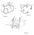
- FIG. 4 is an isometric view of the carrier device of FIG. 2 , with the electronic chip of FIG. 1 installed thereon.
- FIG. 5 is an isometric view showing the underside of the carrier device of FIG. 4 .
- FIG. 6 is a partial isometric view of a holder with the carrier device and chip of FIG. 4 installed thereon.
- FIG. 7 is a partial isometric view of a motor housing with the carrier device and chip of FIG. 4 installed thereon.
- FIG. 8 is a sectional side view of a portion of the holder of FIG. 6 with the carrier device and chip thereon.
- FIG. 1 shows an electronic chip 10 which is an EMI suppression chip, designed as a surface mount component.
- the chip has positive and negative chip contacts 12 , 13 forming contact pads 14 , 16 that lie at laterally L opposite sides of the chip, and has a ground contact 17 with portions in the form of contact pads 20 , 22 on longitudinal M opposite sides of the chip.
- the chip also has top and bottom surfaces 24 , 26 .
- FIG. 2 shows a carrier device or carrier 30 which receives the suppression chip of FIG. 1 in a simple press fit connection.
- the carrier device includes a dielectric (insulative) frame 32 which is shaped as a rectangular container having four side walls 34 respectively labeled 34 A- 34 D and an open top, and with a base 35 .
- the carrier device also includes four sheet metal contact clips 36 , each including an approximately 180° bent part 40 mounted on the top edge 42 of a side wall of the frame.
- Each spring clip has inner and outer tabs 44 , 46 that extend largely downward D from opposite ends of the bent part.
- the inner tabs connect to contact pads of the chip, while the outer tabs connect to terminals of a holder that holds the carrier device.
- the space between the four side walls of the carrier frame, and between the inner tabs of the clips forms a cavity 48 for receiving the chip.
- FIGS. 3A and 3B show spring clips 36 , 36 B of different designs, with the clip of FIG. 3A shown in FIG. 2 .
- the inner tab 44 , 44 B has a locking finger 50 formed by a cutout 52 and bend 54 in the surrounding area 56 of the inner tab. The locking finger is bent to extend at an incline and into a slot of the carrier frame, to hold the clip on the frame.
- the inner tab has a convex bump 58 on its inner face to provide a definite contact location against a holder terminal.
- FIG. 4 shows the electronic chip 10 of FIG. 1 fully installed in the carrier device 30 of FIG. 2 .
- the inner tab of each of four spring clips makes electrical contact with one of the contact pads of the chip, and soldering is not required.
- FIG. 5 shows that the carrier frame has a bottom or base 35 .
- FIG. 5 also shows that each side wall has a recess, or slot 62 for receiving a finger of the inner tab of a clip.
- the inner tabs are biased outward and the locking fingers are securely pressed into the slots.
- the slots can extend fully or only partially into the carrier walls.
- FIG. 6 shows a holder 70 with a housing 72 for receiving the carrier device 30 .
- the holder has positive and negative terminal 74 , 76 , as well as a ground terminal 80 with opposite sides 82 , 84 .
- the terminals form a cradle 78 in the space between the terminals, including the opposite sides of the ground terminal, that receives the carrier device in a push fit with soldering not required.
- FIG. 8 shows that when the carrier device 30 lies in the holder 70 , and with the electronic chip 10 in the carrier device, the tabs 44 , 46 of the spring clips 36 are resiliently deflected toward corresponding carrier walls 34 A, 34 C by a pair of holder terminals 74 , 76 and a pair of chip contact pads 14 , 16 .
- the ground contact pads and terminals that lie at longitudinally opposite sides of the carrier deflect corresponding clips.
- the spring clips provide mechanical retention of the chip in the carrier device and mechanical retention of the carrier device in the holder.
- the clips provide an electrical connection between each chip contact pad and one of the holder terminals, using only a single element which is a clip.
- the approximately 180° bend (135° to 235°) 40 at the top of each clip results in bend part sides 41 that lie closely adjacent to opposite sides of the frame wall.
- the base 35 of the frame of the carrier device projects beyond the side walls. This enables easier latching of the carrier device to the holder.
- FIG. 7 shows an example of a holder in the form of a motor casing 80 which functions as a Faraday cage, with the carrier device 30 mounted in the motor casing.
- the carrier device lies between terminal 82 , 84 of the motor.
- the clips are formed of sheet metal and are preferably plated with a corrosion resistant and conductive material, such as silver.
- the clips are shown mounted by the approximately 180° bent part lying over the top of a carrier wall.
- a clip with inner and outer tabs that are deflected toward a carrier frame wall, can be mounted in other ways.
- the clip can be mounted in a slot of a carrier frame wall.
- the invention provides a means for electrically and mechanically mounting a surface mount electronic chip so it lies securely on a holder and electrically connects to terminals of the holder.
- a carrier device which has walls forming a cavity and which holds a plurality of sheet metal clips at a plurality of the walls.
- Each clip has inner and outer tabs.
- the chip can be installed on the carrier by merely pushing it into the cavity.
- the carrier can be installed on the holder by merely pushing the carrier into a cradle on the carrier formed between terminals of the holder.
- Each clip inner tab is pressed outward by the force of a chip contact pad on an inner tab, and each clip outer tab is pressed inward by the force of a holder terminal against the outer tab.
- the electrical and mechanical connections are made by merely pushing the chip into the carrier device and by merely pushing the carrier device into the cradle formed in the holder (between the holder terminals). Solder connections are not required.
Abstract
Description
Claims (9)
Applications Claiming Priority (2)
| Application Number | Priority Date | Filing Date | Title |
|---|---|---|---|
| GBGB0417204.5 | 2004-08-02 | ||
| GB0417204A GB2416928A (en) | 2004-08-02 | 2004-08-02 | Carrier for compression chip |
Publications (2)
| Publication Number | Publication Date |
|---|---|
| US20060022329A1 US20060022329A1 (en) | 2006-02-02 |
| US7511368B2 true US7511368B2 (en) | 2009-03-31 |
Family
ID=32947854
Family Applications (1)
| Application Number | Title | Priority Date | Filing Date |
|---|---|---|---|
| US11/184,392 Active 2027-01-22 US7511368B2 (en) | 2004-08-02 | 2005-07-19 | Carrier device for electronic chip |
Country Status (6)
| Country | Link |
|---|---|
| US (1) | US7511368B2 (en) |
| EP (1) | EP1624550B1 (en) |
| CN (1) | CN1783665A (en) |
| DE (1) | DE602005000438T2 (en) |
| ES (1) | ES2276378T3 (en) |
| GB (1) | GB2416928A (en) |
Cited By (2)
| Publication number | Priority date | Publication date | Assignee | Title |
|---|---|---|---|---|
| US20130105654A1 (en) * | 2011-10-28 | 2013-05-02 | Hon Hai Precision Industry Co., Ltd. | Fixing apparatus for waveguide plate |
| US20160141131A1 (en) * | 2013-08-30 | 2016-05-19 | Yazaki Corporation | Connection structure of electronic component and terminal metal fittings |
Families Citing this family (7)
| Publication number | Priority date | Publication date | Assignee | Title |
|---|---|---|---|---|
| US7525825B2 (en) * | 2005-09-02 | 2009-04-28 | Gm Global Technology Operations, Inc. | Snap in high power, high current connector with integrated EMI filtering |
| US20080198565A1 (en) * | 2007-02-16 | 2008-08-21 | Tyco Electronics Corporation | Surface mount foot with coined edge surface |
| GB0809764D0 (en) | 2008-05-30 | 2008-07-09 | Johnson Electric Sa | Electric motor |
| DE102011013449B4 (en) * | 2011-03-09 | 2013-12-05 | Continental Automotive Gmbh | Assembly with a carrier, an SMD component and a stamped grid part |
| US8523576B2 (en) | 2011-10-24 | 2013-09-03 | GM Global Technology Operations LLC | Connector for coupling an electric motor to a power source |
| DE102014217924B4 (en) * | 2014-09-08 | 2016-07-28 | Continental Automotive Gmbh | Method for mounting SMD components on contact springs in electric motors |
| JP7310182B2 (en) | 2018-12-25 | 2023-07-19 | Tdk株式会社 | electronic components |
Citations (21)
| Publication number | Priority date | Publication date | Assignee | Title |
|---|---|---|---|---|
| US4037270A (en) * | 1976-05-24 | 1977-07-19 | Control Data Corporation | Circuit packaging and cooling |
| US4089575A (en) | 1976-09-27 | 1978-05-16 | Amp Incorporated | Connector for connecting a circuit element to the surface of a substrate |
| US4378139A (en) | 1981-07-14 | 1983-03-29 | Wells Electronics, Inc. | Integrated circuit carrier connector |
| GB2122429A (en) | 1982-04-08 | 1984-01-11 | Harris Corp | Socket for connecting leadless integrated circuit packages to a printed circuit board |
| US4571015A (en) * | 1984-03-16 | 1986-02-18 | Amp Incorporated | Electrical connector having rotating clamps for securing electronic packages therein |
| US4616895A (en) | 1982-09-29 | 1986-10-14 | Fujitsu Limited | Integrated circuit socket |
| US4639058A (en) * | 1984-08-22 | 1987-01-27 | Minnesota Mining & Manufacturing Co. | Low profile test clip and handle therefor |
| US5226824A (en) * | 1992-05-13 | 1993-07-13 | Foxconn International, Inc. | IC socket and contact therein |
| US5249971A (en) * | 1991-09-13 | 1993-10-05 | Foxconn International, Inc. | IC package connector |
| US5360353A (en) * | 1992-08-28 | 1994-11-01 | Murata Manufacturing Co., Ltd. | Connector |
| JPH08273781A (en) | 1995-03-30 | 1996-10-18 | Oki Electric Ind Co Ltd | Chip part packaging socket |
| US5846098A (en) * | 1995-07-31 | 1998-12-08 | Yazaki Corporation | Capacitor connecting structure and capacitor |
| US6232684B1 (en) | 1999-07-21 | 2001-05-15 | Delphi Technologies, Inc. | Automotive deck lid actuator |
| US20010014548A1 (en) * | 1998-10-20 | 2001-08-16 | Jun Matsukawa | Electrical connector |
| US6319025B1 (en) * | 1997-07-17 | 2001-11-20 | Nec Corporation | Surface installing type connector |
| EP1193839A2 (en) | 2000-08-21 | 2002-04-03 | Johnson Electric S.A. | End cap assembly |
| US6400551B1 (en) * | 2001-05-10 | 2002-06-04 | Ming Chang Lin | Structure of a capacitor |
| US6473291B1 (en) | 1999-03-16 | 2002-10-29 | Gb Aquisition Co., Inc. | Low inductance four terminal capacitor lead frame |
| US6540561B1 (en) * | 1999-10-25 | 2003-04-01 | Japan Aviation Electronic Industry, Ltd. | Locking mechanism for securely preventing disconnection between a plug and a receptacle |
| US6793506B1 (en) * | 2003-08-27 | 2004-09-21 | Molex Incorporated | Board-to-board electrical connector assembly |
| US7156679B1 (en) * | 2005-01-28 | 2007-01-02 | Chen Uei Precision Industry Co., Ltd. | Module connector |
Family Cites Families (2)
| Publication number | Priority date | Publication date | Assignee | Title |
|---|---|---|---|---|
| US6324076B1 (en) * | 1997-05-22 | 2001-11-27 | Fci Americas Technology, Inc. | Electronic card with shield cover having tabs where each tab engages with recess of corresponding shield cover |
| TW359394U (en) * | 1997-07-11 | 1999-05-21 | Hon Hai Prec Ind Co Ltd | Electrinic card device |
-
2004
- 2004-08-02 GB GB0417204A patent/GB2416928A/en not_active Withdrawn
-
2005
- 2005-07-15 DE DE602005000438T patent/DE602005000438T2/en active Active
- 2005-07-15 ES ES05254439T patent/ES2276378T3/en active Active
- 2005-07-15 EP EP05254439A patent/EP1624550B1/en not_active Expired - Fee Related
- 2005-07-19 US US11/184,392 patent/US7511368B2/en active Active
- 2005-08-02 CN CNA200510088260XA patent/CN1783665A/en active Pending
Patent Citations (21)
| Publication number | Priority date | Publication date | Assignee | Title |
|---|---|---|---|---|
| US4037270A (en) * | 1976-05-24 | 1977-07-19 | Control Data Corporation | Circuit packaging and cooling |
| US4089575A (en) | 1976-09-27 | 1978-05-16 | Amp Incorporated | Connector for connecting a circuit element to the surface of a substrate |
| US4378139A (en) | 1981-07-14 | 1983-03-29 | Wells Electronics, Inc. | Integrated circuit carrier connector |
| GB2122429A (en) | 1982-04-08 | 1984-01-11 | Harris Corp | Socket for connecting leadless integrated circuit packages to a printed circuit board |
| US4616895A (en) | 1982-09-29 | 1986-10-14 | Fujitsu Limited | Integrated circuit socket |
| US4571015A (en) * | 1984-03-16 | 1986-02-18 | Amp Incorporated | Electrical connector having rotating clamps for securing electronic packages therein |
| US4639058A (en) * | 1984-08-22 | 1987-01-27 | Minnesota Mining & Manufacturing Co. | Low profile test clip and handle therefor |
| US5249971A (en) * | 1991-09-13 | 1993-10-05 | Foxconn International, Inc. | IC package connector |
| US5226824A (en) * | 1992-05-13 | 1993-07-13 | Foxconn International, Inc. | IC socket and contact therein |
| US5360353A (en) * | 1992-08-28 | 1994-11-01 | Murata Manufacturing Co., Ltd. | Connector |
| JPH08273781A (en) | 1995-03-30 | 1996-10-18 | Oki Electric Ind Co Ltd | Chip part packaging socket |
| US5846098A (en) * | 1995-07-31 | 1998-12-08 | Yazaki Corporation | Capacitor connecting structure and capacitor |
| US6319025B1 (en) * | 1997-07-17 | 2001-11-20 | Nec Corporation | Surface installing type connector |
| US20010014548A1 (en) * | 1998-10-20 | 2001-08-16 | Jun Matsukawa | Electrical connector |
| US6473291B1 (en) | 1999-03-16 | 2002-10-29 | Gb Aquisition Co., Inc. | Low inductance four terminal capacitor lead frame |
| US6232684B1 (en) | 1999-07-21 | 2001-05-15 | Delphi Technologies, Inc. | Automotive deck lid actuator |
| US6540561B1 (en) * | 1999-10-25 | 2003-04-01 | Japan Aviation Electronic Industry, Ltd. | Locking mechanism for securely preventing disconnection between a plug and a receptacle |
| EP1193839A2 (en) | 2000-08-21 | 2002-04-03 | Johnson Electric S.A. | End cap assembly |
| US6400551B1 (en) * | 2001-05-10 | 2002-06-04 | Ming Chang Lin | Structure of a capacitor |
| US6793506B1 (en) * | 2003-08-27 | 2004-09-21 | Molex Incorporated | Board-to-board electrical connector assembly |
| US7156679B1 (en) * | 2005-01-28 | 2007-01-02 | Chen Uei Precision Industry Co., Ltd. | Module connector |
Cited By (4)
| Publication number | Priority date | Publication date | Assignee | Title |
|---|---|---|---|---|
| US20130105654A1 (en) * | 2011-10-28 | 2013-05-02 | Hon Hai Precision Industry Co., Ltd. | Fixing apparatus for waveguide plate |
| US8864090B2 (en) * | 2011-10-28 | 2014-10-21 | Hong Fu Jin Precision Industry (Shenzhen) Co., Ltd. | Fixing apparatus for waveguide plate |
| US20160141131A1 (en) * | 2013-08-30 | 2016-05-19 | Yazaki Corporation | Connection structure of electronic component and terminal metal fittings |
| US9520255B2 (en) * | 2013-08-30 | 2016-12-13 | Yazaki Corporation | Connection structure of electronic component and terminal metal fittings |
Also Published As
| Publication number | Publication date |
|---|---|
| EP1624550B1 (en) | 2007-01-10 |
| GB2416928A (en) | 2006-02-08 |
| DE602005000438D1 (en) | 2007-02-22 |
| DE602005000438T2 (en) | 2007-10-31 |
| GB0417204D0 (en) | 2004-09-01 |
| EP1624550A1 (en) | 2006-02-08 |
| US20060022329A1 (en) | 2006-02-02 |
| CN1783665A (en) | 2006-06-07 |
| ES2276378T3 (en) | 2007-06-16 |
Similar Documents
| Publication | Publication Date | Title |
|---|---|---|
| US7511368B2 (en) | Carrier device for electronic chip | |
| US7435139B2 (en) | Electrical connector having improved shield | |
| US20050215087A1 (en) | Electronic part-mounting socket | |
| US20080014797A1 (en) | Electrical connector with reliable shielding member | |
| KR20020000004U (en) | Surface mount electrical connector | |
| JP3959529B2 (en) | Socket for mounting electronic components | |
| US5463531A (en) | PCMCIA electronics housing | |
| US20020193006A1 (en) | Sink-type audio socket connector having improved grounding structure | |
| US11769961B2 (en) | Electrical connector module and heat dissipation housing | |
| US7269033B2 (en) | Suppressor device | |
| EP1803195A1 (en) | Socket for digital camera module | |
| JP6960996B2 (en) | Electronic device | |
| US20070077804A1 (en) | Electrical connector | |
| US20080242126A1 (en) | Circuit board assembly | |
| KR200145503Y1 (en) | Earth system for ic card | |
| US20220087070A1 (en) | Electrical connector module and heat dissipation housing | |
| US8279028B2 (en) | Electromagnetic relay | |
| US6875055B2 (en) | Electrical connector | |
| US20020039285A1 (en) | Device for reducing electromagnetic interference in a processor assembly | |
| US11553607B2 (en) | Electronic device | |
| US20220294161A1 (en) | Conductive housing for connector and Connector comprising the same | |
| EP3945662A1 (en) | Dc motor arrangement for an automotive wiper | |
| JP2005032568A (en) | Socket device | |
| KR20150070038A (en) | Planar transformer and electrical component | |
| JPS6091577A (en) | Device for connecting leadless flat circuit and connector |
Legal Events
| Date | Code | Title | Description |
|---|---|---|---|
| AS | Assignment |
Owner name: ITT MANUFACTURING ENTERPRISES, INC., DELAWARE Free format text: ASSIGNMENT OF ASSIGNORS INTEREST;ASSIGNOR:JORDAN, PETER;REEL/FRAME:016789/0356 Effective date: 20050719 |
|
| STCF | Information on status: patent grant |
Free format text: PATENTED CASE |
|
| FPAY | Fee payment |
Year of fee payment: 4 |
|
| FPAY | Fee payment |
Year of fee payment: 8 |
|
| MAFP | Maintenance fee payment |
Free format text: PAYMENT OF MAINTENANCE FEE, 12TH YEAR, LARGE ENTITY (ORIGINAL EVENT CODE: M1553); ENTITY STATUS OF PATENT OWNER: LARGE ENTITY Year of fee payment: 12 |