US7488622B2 - Method for producing a surface-mountable semiconductor component - Google Patents
Method for producing a surface-mountable semiconductor component Download PDFInfo
- Publication number
- US7488622B2 US7488622B2 US11/731,911 US73191107A US7488622B2 US 7488622 B2 US7488622 B2 US 7488622B2 US 73191107 A US73191107 A US 73191107A US 7488622 B2 US7488622 B2 US 7488622B2
- Authority
- US
- United States
- Prior art keywords
- encapsulation material
- array
- film
- film strip
- semiconductor chip
- Prior art date
- Legal status (The legal status is an assumption and is not a legal conclusion. Google has not performed a legal analysis and makes no representation as to the accuracy of the status listed.)
- Expired - Fee Related, expires
Links
Images


Classifications
-
- H—ELECTRICITY
- H01—ELECTRIC ELEMENTS
- H01L—SEMICONDUCTOR DEVICES NOT COVERED BY CLASS H10
- H01L21/00—Processes or apparatus adapted for the manufacture or treatment of semiconductor or solid state devices or of parts thereof
- H01L21/02—Manufacture or treatment of semiconductor devices or of parts thereof
- H01L21/04—Manufacture or treatment of semiconductor devices or of parts thereof the devices having at least one potential-jump barrier or surface barrier, e.g. PN junction, depletion layer or carrier concentration layer
- H01L21/50—Assembly of semiconductor devices using processes or apparatus not provided for in a single one of the subgroups H01L21/06 - H01L21/326, e.g. sealing of a cap to a base of a container
- H01L21/56—Encapsulations, e.g. encapsulation layers, coatings
- H01L21/561—Batch processing
-
- H—ELECTRICITY
- H01—ELECTRIC ELEMENTS
- H01L—SEMICONDUCTOR DEVICES NOT COVERED BY CLASS H10
- H01L21/00—Processes or apparatus adapted for the manufacture or treatment of semiconductor or solid state devices or of parts thereof
- H01L21/02—Manufacture or treatment of semiconductor devices or of parts thereof
- H01L21/04—Manufacture or treatment of semiconductor devices or of parts thereof the devices having at least one potential-jump barrier or surface barrier, e.g. PN junction, depletion layer or carrier concentration layer
- H01L21/50—Assembly of semiconductor devices using processes or apparatus not provided for in a single one of the subgroups H01L21/06 - H01L21/326, e.g. sealing of a cap to a base of a container
- H01L21/56—Encapsulations, e.g. encapsulation layers, coatings
- H01L21/565—Moulds
-
- H—ELECTRICITY
- H01—ELECTRIC ELEMENTS
- H01L—SEMICONDUCTOR DEVICES NOT COVERED BY CLASS H10
- H01L23/00—Details of semiconductor or other solid state devices
- H01L23/28—Encapsulations, e.g. encapsulating layers, coatings, e.g. for protection
- H01L23/31—Encapsulations, e.g. encapsulating layers, coatings, e.g. for protection characterised by the arrangement or shape
- H01L23/3107—Encapsulations, e.g. encapsulating layers, coatings, e.g. for protection characterised by the arrangement or shape the device being completely enclosed
- H01L23/3121—Encapsulations, e.g. encapsulating layers, coatings, e.g. for protection characterised by the arrangement or shape the device being completely enclosed a substrate forming part of the encapsulation
-
- H—ELECTRICITY
- H01—ELECTRIC ELEMENTS
- H01L—SEMICONDUCTOR DEVICES NOT COVERED BY CLASS H10
- H01L23/00—Details of semiconductor or other solid state devices
- H01L23/48—Arrangements for conducting electric current to or from the solid state body in operation, e.g. leads, terminal arrangements ; Selection of materials therefor
- H01L23/488—Arrangements for conducting electric current to or from the solid state body in operation, e.g. leads, terminal arrangements ; Selection of materials therefor consisting of soldered or bonded constructions
- H01L23/498—Leads, i.e. metallisations or lead-frames on insulating substrates, e.g. chip carriers
- H01L23/49838—Geometry or layout
-
- H—ELECTRICITY
- H01—ELECTRIC ELEMENTS
- H01L—SEMICONDUCTOR DEVICES NOT COVERED BY CLASS H10
- H01L23/00—Details of semiconductor or other solid state devices
- H01L23/48—Arrangements for conducting electric current to or from the solid state body in operation, e.g. leads, terminal arrangements ; Selection of materials therefor
- H01L23/488—Arrangements for conducting electric current to or from the solid state body in operation, e.g. leads, terminal arrangements ; Selection of materials therefor consisting of soldered or bonded constructions
- H01L23/498—Leads, i.e. metallisations or lead-frames on insulating substrates, e.g. chip carriers
- H01L23/4985—Flexible insulating substrates
-
- H—ELECTRICITY
- H01—ELECTRIC ELEMENTS
- H01L—SEMICONDUCTOR DEVICES NOT COVERED BY CLASS H10
- H01L24/00—Arrangements for connecting or disconnecting semiconductor or solid-state bodies; Methods or apparatus related thereto
- H01L24/93—Batch processes
- H01L24/95—Batch processes at chip-level, i.e. with connecting carried out on a plurality of singulated devices, i.e. on diced chips
- H01L24/97—Batch processes at chip-level, i.e. with connecting carried out on a plurality of singulated devices, i.e. on diced chips the devices being connected to a common substrate, e.g. interposer, said common substrate being separable into individual assemblies after connecting
-
- H—ELECTRICITY
- H01—ELECTRIC ELEMENTS
- H01L—SEMICONDUCTOR DEVICES NOT COVERED BY CLASS H10
- H01L33/00—Semiconductor devices with at least one potential-jump barrier or surface barrier specially adapted for light emission; Processes or apparatus specially adapted for the manufacture or treatment thereof or of parts thereof; Details thereof
- H01L33/48—Semiconductor devices with at least one potential-jump barrier or surface barrier specially adapted for light emission; Processes or apparatus specially adapted for the manufacture or treatment thereof or of parts thereof; Details thereof characterised by the semiconductor body packages
- H01L33/483—Containers
- H01L33/486—Containers adapted for surface mounting
-
- H—ELECTRICITY
- H01—ELECTRIC ELEMENTS
- H01L—SEMICONDUCTOR DEVICES NOT COVERED BY CLASS H10
- H01L33/00—Semiconductor devices with at least one potential-jump barrier or surface barrier specially adapted for light emission; Processes or apparatus specially adapted for the manufacture or treatment thereof or of parts thereof; Details thereof
- H01L33/48—Semiconductor devices with at least one potential-jump barrier or surface barrier specially adapted for light emission; Processes or apparatus specially adapted for the manufacture or treatment thereof or of parts thereof; Details thereof characterised by the semiconductor body packages
- H01L33/62—Arrangements for conducting electric current to or from the semiconductor body, e.g. lead-frames, wire-bonds or solder balls
-
- H—ELECTRICITY
- H01—ELECTRIC ELEMENTS
- H01L—SEMICONDUCTOR DEVICES NOT COVERED BY CLASS H10
- H01L2224/00—Indexing scheme for arrangements for connecting or disconnecting semiconductor or solid-state bodies and methods related thereto as covered by H01L24/00
- H01L2224/01—Means for bonding being attached to, or being formed on, the surface to be connected, e.g. chip-to-package, die-attach, "first-level" interconnects; Manufacturing methods related thereto
- H01L2224/02—Bonding areas; Manufacturing methods related thereto
- H01L2224/04—Structure, shape, material or disposition of the bonding areas prior to the connecting process
- H01L2224/05—Structure, shape, material or disposition of the bonding areas prior to the connecting process of an individual bonding area
- H01L2224/0554—External layer
- H01L2224/05599—Material
-
- H—ELECTRICITY
- H01—ELECTRIC ELEMENTS
- H01L—SEMICONDUCTOR DEVICES NOT COVERED BY CLASS H10
- H01L2224/00—Indexing scheme for arrangements for connecting or disconnecting semiconductor or solid-state bodies and methods related thereto as covered by H01L24/00
- H01L2224/01—Means for bonding being attached to, or being formed on, the surface to be connected, e.g. chip-to-package, die-attach, "first-level" interconnects; Manufacturing methods related thereto
- H01L2224/42—Wire connectors; Manufacturing methods related thereto
- H01L2224/44—Structure, shape, material or disposition of the wire connectors prior to the connecting process
- H01L2224/45—Structure, shape, material or disposition of the wire connectors prior to the connecting process of an individual wire connector
- H01L2224/45001—Core members of the connector
- H01L2224/45099—Material
-
- H—ELECTRICITY
- H01—ELECTRIC ELEMENTS
- H01L—SEMICONDUCTOR DEVICES NOT COVERED BY CLASS H10
- H01L2224/00—Indexing scheme for arrangements for connecting or disconnecting semiconductor or solid-state bodies and methods related thereto as covered by H01L24/00
- H01L2224/01—Means for bonding being attached to, or being formed on, the surface to be connected, e.g. chip-to-package, die-attach, "first-level" interconnects; Manufacturing methods related thereto
- H01L2224/42—Wire connectors; Manufacturing methods related thereto
- H01L2224/47—Structure, shape, material or disposition of the wire connectors after the connecting process
- H01L2224/48—Structure, shape, material or disposition of the wire connectors after the connecting process of an individual wire connector
- H01L2224/4805—Shape
- H01L2224/4809—Loop shape
- H01L2224/48091—Arched
-
- H—ELECTRICITY
- H01—ELECTRIC ELEMENTS
- H01L—SEMICONDUCTOR DEVICES NOT COVERED BY CLASS H10
- H01L2224/00—Indexing scheme for arrangements for connecting or disconnecting semiconductor or solid-state bodies and methods related thereto as covered by H01L24/00
- H01L2224/01—Means for bonding being attached to, or being formed on, the surface to be connected, e.g. chip-to-package, die-attach, "first-level" interconnects; Manufacturing methods related thereto
- H01L2224/42—Wire connectors; Manufacturing methods related thereto
- H01L2224/47—Structure, shape, material or disposition of the wire connectors after the connecting process
- H01L2224/48—Structure, shape, material or disposition of the wire connectors after the connecting process of an individual wire connector
- H01L2224/481—Disposition
- H01L2224/48151—Connecting between a semiconductor or solid-state body and an item not being a semiconductor or solid-state body, e.g. chip-to-substrate, chip-to-passive
- H01L2224/48221—Connecting between a semiconductor or solid-state body and an item not being a semiconductor or solid-state body, e.g. chip-to-substrate, chip-to-passive the body and the item being stacked
- H01L2224/48225—Connecting between a semiconductor or solid-state body and an item not being a semiconductor or solid-state body, e.g. chip-to-substrate, chip-to-passive the body and the item being stacked the item being non-metallic, e.g. insulating substrate with or without metallisation
- H01L2224/48227—Connecting between a semiconductor or solid-state body and an item not being a semiconductor or solid-state body, e.g. chip-to-substrate, chip-to-passive the body and the item being stacked the item being non-metallic, e.g. insulating substrate with or without metallisation connecting the wire to a bond pad of the item
-
- H—ELECTRICITY
- H01—ELECTRIC ELEMENTS
- H01L—SEMICONDUCTOR DEVICES NOT COVERED BY CLASS H10
- H01L2224/00—Indexing scheme for arrangements for connecting or disconnecting semiconductor or solid-state bodies and methods related thereto as covered by H01L24/00
- H01L2224/80—Methods for connecting semiconductor or other solid state bodies using means for bonding being attached to, or being formed on, the surface to be connected
- H01L2224/85—Methods for connecting semiconductor or other solid state bodies using means for bonding being attached to, or being formed on, the surface to be connected using a wire connector
- H01L2224/8538—Bonding interfaces outside the semiconductor or solid-state body
- H01L2224/85399—Material
-
- H—ELECTRICITY
- H01—ELECTRIC ELEMENTS
- H01L—SEMICONDUCTOR DEVICES NOT COVERED BY CLASS H10
- H01L2224/00—Indexing scheme for arrangements for connecting or disconnecting semiconductor or solid-state bodies and methods related thereto as covered by H01L24/00
- H01L2224/93—Batch processes
- H01L2224/95—Batch processes at chip-level, i.e. with connecting carried out on a plurality of singulated devices, i.e. on diced chips
- H01L2224/97—Batch processes at chip-level, i.e. with connecting carried out on a plurality of singulated devices, i.e. on diced chips the devices being connected to a common substrate, e.g. interposer, said common substrate being separable into individual assemblies after connecting
-
- H—ELECTRICITY
- H01—ELECTRIC ELEMENTS
- H01L—SEMICONDUCTOR DEVICES NOT COVERED BY CLASS H10
- H01L24/00—Arrangements for connecting or disconnecting semiconductor or solid-state bodies; Methods or apparatus related thereto
- H01L24/01—Means for bonding being attached to, or being formed on, the surface to be connected, e.g. chip-to-package, die-attach, "first-level" interconnects; Manufacturing methods related thereto
- H01L24/42—Wire connectors; Manufacturing methods related thereto
- H01L24/47—Structure, shape, material or disposition of the wire connectors after the connecting process
- H01L24/48—Structure, shape, material or disposition of the wire connectors after the connecting process of an individual wire connector
-
- H—ELECTRICITY
- H01—ELECTRIC ELEMENTS
- H01L—SEMICONDUCTOR DEVICES NOT COVERED BY CLASS H10
- H01L2924/00—Indexing scheme for arrangements or methods for connecting or disconnecting semiconductor or solid-state bodies as covered by H01L24/00
- H01L2924/0001—Technical content checked by a classifier
- H01L2924/00014—Technical content checked by a classifier the subject-matter covered by the group, the symbol of which is combined with the symbol of this group, being disclosed without further technical details
-
- H—ELECTRICITY
- H01—ELECTRIC ELEMENTS
- H01L—SEMICONDUCTOR DEVICES NOT COVERED BY CLASS H10
- H01L2924/00—Indexing scheme for arrangements or methods for connecting or disconnecting semiconductor or solid-state bodies as covered by H01L24/00
- H01L2924/01—Chemical elements
- H01L2924/01004—Beryllium [Be]
-
- H—ELECTRICITY
- H01—ELECTRIC ELEMENTS
- H01L—SEMICONDUCTOR DEVICES NOT COVERED BY CLASS H10
- H01L2924/00—Indexing scheme for arrangements or methods for connecting or disconnecting semiconductor or solid-state bodies as covered by H01L24/00
- H01L2924/01—Chemical elements
- H01L2924/01005—Boron [B]
-
- H—ELECTRICITY
- H01—ELECTRIC ELEMENTS
- H01L—SEMICONDUCTOR DEVICES NOT COVERED BY CLASS H10
- H01L2924/00—Indexing scheme for arrangements or methods for connecting or disconnecting semiconductor or solid-state bodies as covered by H01L24/00
- H01L2924/01—Chemical elements
- H01L2924/01006—Carbon [C]
-
- H—ELECTRICITY
- H01—ELECTRIC ELEMENTS
- H01L—SEMICONDUCTOR DEVICES NOT COVERED BY CLASS H10
- H01L2924/00—Indexing scheme for arrangements or methods for connecting or disconnecting semiconductor or solid-state bodies as covered by H01L24/00
- H01L2924/01—Chemical elements
- H01L2924/01015—Phosphorus [P]
-
- H—ELECTRICITY
- H01—ELECTRIC ELEMENTS
- H01L—SEMICONDUCTOR DEVICES NOT COVERED BY CLASS H10
- H01L2924/00—Indexing scheme for arrangements or methods for connecting or disconnecting semiconductor or solid-state bodies as covered by H01L24/00
- H01L2924/01—Chemical elements
- H01L2924/01029—Copper [Cu]
-
- H—ELECTRICITY
- H01—ELECTRIC ELEMENTS
- H01L—SEMICONDUCTOR DEVICES NOT COVERED BY CLASS H10
- H01L2924/00—Indexing scheme for arrangements or methods for connecting or disconnecting semiconductor or solid-state bodies as covered by H01L24/00
- H01L2924/01—Chemical elements
- H01L2924/01032—Germanium [Ge]
-
- H—ELECTRICITY
- H01—ELECTRIC ELEMENTS
- H01L—SEMICONDUCTOR DEVICES NOT COVERED BY CLASS H10
- H01L2924/00—Indexing scheme for arrangements or methods for connecting or disconnecting semiconductor or solid-state bodies as covered by H01L24/00
- H01L2924/01—Chemical elements
- H01L2924/01033—Arsenic [As]
-
- H—ELECTRICITY
- H01—ELECTRIC ELEMENTS
- H01L—SEMICONDUCTOR DEVICES NOT COVERED BY CLASS H10
- H01L2924/00—Indexing scheme for arrangements or methods for connecting or disconnecting semiconductor or solid-state bodies as covered by H01L24/00
- H01L2924/01—Chemical elements
- H01L2924/01061—Promethium [Pm]
-
- H—ELECTRICITY
- H01—ELECTRIC ELEMENTS
- H01L—SEMICONDUCTOR DEVICES NOT COVERED BY CLASS H10
- H01L2924/00—Indexing scheme for arrangements or methods for connecting or disconnecting semiconductor or solid-state bodies as covered by H01L24/00
- H01L2924/01—Chemical elements
- H01L2924/01068—Erbium [Er]
-
- H—ELECTRICITY
- H01—ELECTRIC ELEMENTS
- H01L—SEMICONDUCTOR DEVICES NOT COVERED BY CLASS H10
- H01L2924/00—Indexing scheme for arrangements or methods for connecting or disconnecting semiconductor or solid-state bodies as covered by H01L24/00
- H01L2924/01—Chemical elements
- H01L2924/01075—Rhenium [Re]
-
- H—ELECTRICITY
- H01—ELECTRIC ELEMENTS
- H01L—SEMICONDUCTOR DEVICES NOT COVERED BY CLASS H10
- H01L2924/00—Indexing scheme for arrangements or methods for connecting or disconnecting semiconductor or solid-state bodies as covered by H01L24/00
- H01L2924/01—Chemical elements
- H01L2924/01079—Gold [Au]
-
- H—ELECTRICITY
- H01—ELECTRIC ELEMENTS
- H01L—SEMICONDUCTOR DEVICES NOT COVERED BY CLASS H10
- H01L2924/00—Indexing scheme for arrangements or methods for connecting or disconnecting semiconductor or solid-state bodies as covered by H01L24/00
- H01L2924/01—Chemical elements
- H01L2924/01082—Lead [Pb]
-
- H—ELECTRICITY
- H01—ELECTRIC ELEMENTS
- H01L—SEMICONDUCTOR DEVICES NOT COVERED BY CLASS H10
- H01L2924/00—Indexing scheme for arrangements or methods for connecting or disconnecting semiconductor or solid-state bodies as covered by H01L24/00
- H01L2924/01—Chemical elements
- H01L2924/01084—Polonium [Po]
-
- H—ELECTRICITY
- H01—ELECTRIC ELEMENTS
- H01L—SEMICONDUCTOR DEVICES NOT COVERED BY CLASS H10
- H01L2924/00—Indexing scheme for arrangements or methods for connecting or disconnecting semiconductor or solid-state bodies as covered by H01L24/00
- H01L2924/10—Details of semiconductor or other solid state devices to be connected
- H01L2924/11—Device type
- H01L2924/12—Passive devices, e.g. 2 terminal devices
- H01L2924/1204—Optical Diode
- H01L2924/12041—LED
-
- H—ELECTRICITY
- H01—ELECTRIC ELEMENTS
- H01L—SEMICONDUCTOR DEVICES NOT COVERED BY CLASS H10
- H01L2924/00—Indexing scheme for arrangements or methods for connecting or disconnecting semiconductor or solid-state bodies as covered by H01L24/00
- H01L2924/10—Details of semiconductor or other solid state devices to be connected
- H01L2924/11—Device type
- H01L2924/12—Passive devices, e.g. 2 terminal devices
- H01L2924/1204—Optical Diode
- H01L2924/12042—LASER
-
- H—ELECTRICITY
- H01—ELECTRIC ELEMENTS
- H01L—SEMICONDUCTOR DEVICES NOT COVERED BY CLASS H10
- H01L2924/00—Indexing scheme for arrangements or methods for connecting or disconnecting semiconductor or solid-state bodies as covered by H01L24/00
- H01L2924/10—Details of semiconductor or other solid state devices to be connected
- H01L2924/11—Device type
- H01L2924/12—Passive devices, e.g. 2 terminal devices
- H01L2924/1204—Optical Diode
- H01L2924/12043—Photo diode
-
- H—ELECTRICITY
- H01—ELECTRIC ELEMENTS
- H01L—SEMICONDUCTOR DEVICES NOT COVERED BY CLASS H10
- H01L2924/00—Indexing scheme for arrangements or methods for connecting or disconnecting semiconductor or solid-state bodies as covered by H01L24/00
- H01L2924/15—Details of package parts other than the semiconductor or other solid state devices to be connected
- H01L2924/181—Encapsulation
Definitions
- the invention relates to a method for producing a surface-mountable semiconductor component having a semiconductor chip, at least two external electrical connections, which are electrically conductively connected to at least two electrical contacts of the semiconductor chip, and an encapsulation material.
- Luminescence diode housings with an installation area dimensioned as 0402 (corresponding to 0.5 mm ⁇ 1.0 mm) and a device height of 400 ⁇ m-600 ⁇ m have become available in the meantime. See the data sheet from FAIRCHILD SEMICONDUCTOR® concerning the QTLP690C-x design. The corresponding device concept is described in the document U.S. Pat. No. 4,843,280.
- One object of the present invention is to provide a surface-mountable semiconductor component, in particular a surface-mountable miniature luminescence diode and/or photo diode, which permits the structural size to be reduced more extensively.
- a surface-mountable semiconductor component comprising a semiconductor chip, at least two external electrical connections, which are electrically conductively connected to at least two electrical contacts of the semiconductor chip, and a chip encapsulation material.
- the two external electrical connections are formed at a film having a thickness of less than or equal to 100 ⁇ m.
- the semiconductor chip is fixed at a first surface of the film, and the encapsulation material is applied on the first surface.
- Designs with a very small structural height can be obtained by mounting the semiconductor chip on a very thin film on which the external electrical connections are formed, which designs can, moreover, be produced with high packing density and thus with low production costs.
- the design according to an embodiment of the invention is, for example, suitable for application in electromagnetic radiation emitting and/or receiving components having one or more electromagnetic radiation emitting and/or receiving semiconductor chips, in particular for luminescence diode components having a housing installation area dimensioned as 0402 (corresponding to 0.5 mm ⁇ 1.0 mm) or less and a device height of less than 400 ⁇ m in particular less than 350 ⁇ m.
- the encapsulation material is produced from an electromagnetic radiation-transmissive, in particular transparent or translucent material, in particular from an electromagnetic radiation-transmissive, preferably unfilled clear plastic material.
- the encapsulation material may be admixed with a phosphor that absorbs at least a portion of the electromagnetic radiation emitted by the luminescence diode chip and emits electromagnetic radiation having a different wavelength and color than the absorbed radiation.
- the encapsulation material is preferably produced by means of an injection-molding method.
- the film including the external electrical connections, on the side on which the semiconductor chips are arranged can be coated with a covering layer that is adhesion-promoting with respect to the encapsulation material and has mounting windows at the chip mounting locations and at the wire mounting locations, no covering layer being present in said mounting windows.
- two external electrical connections are in each case formed by a first electrical connection region on the first main area of the film, a second electrical connection region on the second main area of the film and at least one electrical leadthrough through the film, which electrically connects the first connection region to the associated second connection region.
- the electrical connection regions can be produced by means of patterned metal layers on the film. Conventional suitable methods can be used for patterning the metal layers.
- the metal layers are constructed in multilayered fashion and preferably have, as seen from the film, a first layer made of copper or a copper based alloy, which is responsible for the electrical conduction of the metal layer, a second layer made of nickel or a nickel based alloy, which constitutes a barrier layer, and a third layer made of gold or a gold based alloy, which serves for improving the bondability and solderability of the metal layer.
- the metal layers situated on the chip side preferably have, as seen from the plastic film, a copper layer followed by a nickel layer, on which, in turn, an NiP layer (phosphorus content for example between 5% and 15%, preferably 8%) is applied.
- the NiP layer advantageously has a higher reflectivity than an Ni layer and its bondability is at least similarly as good as that of an Ni layer. Moreover, it advantageously has a significantly lower tendency to tarnishing (oxidizing) than an Ni layer.
- the metal layers situated on the rear side of the leadframe then have the same layer sequence, as seen from the plastic layer, in order in particular to simplify the production of the leadframe. In order to increase the storage stability, a gold layer may preferably be applied to the NiP layer.
- the first layer has a thickness of between 5 ⁇ m and 25 ⁇ m inclusive.
- the latter is fixed on one of the two first electrical connection regions by means of a connecting means having good thermal conductivity and the corresponding external electrical connection is formed in such a way that it constitutes a sufficiently good thermal connection for the semiconductor chip.
- a connecting means having good thermal conductivity and the corresponding external electrical connection is formed in such a way that it constitutes a sufficiently good thermal connection for the semiconductor chip.
- the semiconductor chip may be mounted onto the associated electrical connection region both by its substrate side (i.e. upside up mounting) and by its epitaxial layer side (upside down or flip-chip mounting).
- the connecting means is, by way of example, a sufficiently thermally conductive adhesive or a metallic solder.
- the encapsulation material preferably has, in an edge region toward its lateral edge as seen in the perpendicular direction with respect to the film, a smaller thickness than in a central region that spans at least the semiconductor chip and, if appropriate, one or more bonding wires to the light-emitting diode chip. This advantageously reduces the volume of the encapsulation material, as a result of which it is possible to counteract a warpage of the film during the production method on account of different thermal expansions of film and encapsulation material.
- the mutually opposite ends of the external electrical connections have regions that project in each case in an offset manner with respect to one another, the electrical leadthroughs through the film being arranged in said regions.
- the mutually opposite ends of the external electrical connections can run in an S-like manner such that the projecting parts overlap.
- Another aspect of the present invention directed to a method for simultaneously producing a multiplicity of surface-mountable semiconductor components each having at least one semiconductor chip, at least two external electrical connections, which are electrically conductively connected to at least two electrical contacts of the semiconductor chip, and an encapsulation material.
- a film strip is provided which has on both sides electrically conductive layers that are patterned and through-connected through the film strip in such a way that an array comprising a multiplicity of component region arranged next to one another is formed.
- Each of the component regions includes structures of the electrically conductive layers for the at least two external electrical connections.
- At least one semiconductor chip is applied on each of the component regions and the semiconductor chip is electrically connected to the associated external electrical connections.
- the array is introduced into an injection mold, in which a single cavity which spans all the semiconductor chips of the array and forms a void there essentially exclusively on the side of the semiconductor chips is provided for an array.
- Encapsulation material is injected into the cavity and at least partially cured before removing the array from the injection mold.
- the array is singulated into individual semiconductor components by means of severing the encapsulation material and the film strip with the patterned electrically conductive layers between the component regions.
- the cavity has a multiplicity of cutouts in each case spanning one or more semiconductor chips.
- the volume of encapsulation material is reduced in that the thickness of the encapsulation material is reduced in regions where this is permissible compared with the thickness in the region of semiconductor chips and, if appropriate, one or more bonding wires to the semiconductor chip.
- a separate cutout can be provided above each semiconductor chip of the array in such a way that the encapsulation material has, after the injection-molding process, a multiplicity of elevations arranged next to one another, in particular a structure similar to a chocolate bar.
- the array is singulated by means of severing the encapsulation material and the film strip with the patterned electrically conductive layers in the trenches between the elevations.
- an adhesion promoter is applied to the film and/or the electrically conductive layers, which adhesion promoter improves the adhesion of the encapsulation material on the film and/or the electrically conductive layers.
- a PI covering coating is preferably used for this purpose.
- the adhesion promoter is preferably in each case applied to the entire component region, except for the chip mounting regions, on which the semiconductor chips are fixed, and, if appropriate, the wire mounting regions, on which connection wires are fixed.
- the adhesion promoter has contact-making windows in these regions.
- the film strip with the patterned electrically conductive layers is laminated onto an auxiliary film by its rear side prior to introduction into the injection mold.
- Said auxiliary film protects the electrical connections on the one hand against mechanical damage (e.g. scratching) and on the other hand against undesirable covering of the connections with encapsulation material, that is to say against a so-called flash on the rear side of the film strip.
- the auxiliary film expediently has a coefficient of thermal expansion which is similar to or greater than that of the encapsulation material in such a way that it counteracts to the greatest possible extent a warpage of the array on account of shrinkage of the encapsulation material to a greater extent than the film strip during the curing and/or cooling of said encapsulation material after the array has been encapsulated by injection molding.
- the film strip may have, outside the arrays, holes, perforations and/or slots for reducing mechanical strains on account of different thermal expansions and/or material shrinkages.
- the film strip may be composed of a material that has a coefficient of thermal expansion similar to that of the encapsulation material.
- the array is applied to a film by the encapsulation side prior to singulation and afterward, if appropriate, the auxiliary film is stripped from the rear side of the film.
- said film is preferably transmissive to electromagnetic radiation and the measurement is effected through the film.
- the array is preferably singulated by means of sawing, laser separation and/or water jet cutting.
- an embodiment of the invention affords the possibility of dispensing with taping of the devices.
- a plurality of associated devices may be supplied after a chip test on the flexible frame together with a wafer map.
- the devices may be singulated, taped and supplied as before after the chip test.
- FIG. 1 shows a schematic sectional view through the semiconductor component in accordance with the exemplary embodiment
- FIG. 2 shows a schematic illustration of a plan view of the front side of a detail from a film strip
- FIG. 3 shows a schematic illustration of a plan view of the rear side of the detail from FIG. 2 ;
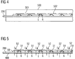
- FIG. 4 shows a partial schematic illustration of a sectional view of an injection mold with an introduced film strip
- FIG. 5 shows a partial schematic illustration of a sectional view of a film strip with encapsulated semiconductor chips
- FIG. 6 shows a partial schematic illustration of a plan view of a film strip with encapsulated semiconductor chips
- FIG. 7 shows an enlarged schematic illustration of a detail from the film strip illustrated in FIG. 6 .
- the semiconductor component according to the invention as illustrated in FIG. 1 is a surface-mountable miniature light-emitting diode component having a footprint of the 0402 type.
- two external electrical connections 3 , 4 are formed on a plastic film 2 , which is made for example of polyimide (PI) or polyethylene naphthalate (PEN).
- the thickness of the plastic film 2 is approximately 50 ⁇ m or less.
- a light-emitting diode chip 1 is fixed at an upper surface 22 of the plastic film 2 and is encapsulated there with an encapsulation material 50 applied on the upper surface 22 .
- the encapsulation material 50 is preferably composed of a clear plastic material, preferably an unfilled clear epoxy resin material, which can be processed by means of injection molding or transfer molding.
- the two external electrical connections 3 , 4 in each case comprise a first metalized region 31 , 32 on the upper surface 22 of the film 2 , a second metalized region 41 , 42 on a lower surface 23 of the film 2 and at least one metallic electrical leadthrough 314 , 324 through the film 2 , which respectively electrically connect the first metalized region 31 , 32 to the associated second metalized region 41 , 42 .
- the metalized regions 31 , 32 , 41 and 42 in each case have a plurality of layers and contain, as seen from the film 2 , successively an electrical conduction layer having copper or a copper based alloy and a barrier layer having nickel or a nickel based alloy.
- a connection layer having gold or a gold based alloy is in each case situated on the barrier layer for the purpose of improving the bondability or solderability.
- Copper based alloy, nickel based alloy and gold based alloy are to be understood to mean all alloys whose properties are substantially determined by copper, nickel and gold, respectively.
- the metalized regions 31 and 32 situated on the upper surface 22 preferably have, as seen from the plastic film 2 , a copper layer followed by a nickel layer, on which, in turn, an NiP layer (phosphorus content for example between 5% and 15%, preferably 8%) is applied.
- the NiP layer advantageously has a higher reflectivity than an Ni layer and its bondability is at least similarly as good as that of an Ni layer. Moreover, it advantageously has a significantly lower tendency to tarnishing (oxidizing) than an Ni layer.
- the metalized regions 41 and 42 situated on the lower surface 23 preferably have the same layer sequence of metalized regions 31 and 32 as seen from the plastic layer 2 .
- a gold layer may preferably be applied to the NiP layer.
- the thickness of the electrical conduction layer lies between 5 and 25 ⁇ m inclusive.
- the light-emitting diode chip 1 is fixed on the electrical connection region 31 by means of a connecting means having good thermal conductivity and the associated external electrical connection 31 , 314 , 41 is formed in such a way that it can be utilized as a thermal connection for the light-emitting diode chip.
- the light-emitting diode chip can be mounted onto the electrical connection region 31 both by its substrate side (i.e. upside up mounting) and by its epitaxial layer side (upside down or flip-chip mounting).
- the connecting means is, by way of example, a sufficiently thermally conductive adhesive or a metallic solder.
- the encapsulation material 50 preferably has, in an edge region 52 (see FIG. 5 ) toward its lateral edge as seen in the perpendicular direction with respect to the film, a smaller thickness than in a central region 51 (see FIG. 5 ) that spans at least the semiconductor chip 1 and, if appropriate, one or more bonding wires 6 to the light-emitting diode chip 1 . This is indicated by the dashed lines 53 , 54 in FIG. 1 and can be seen from FIGS. 5 , 6 and 7 .
- the lateral dimensions of the surface-mountable light-emitting diode component are at most 0.5 mm ⁇ 1 mm and the device height is less than or equal to 0.4 mm, preferably less than or equal to 0.35 mm.
- the encapsulation material may be admixed with a phosphor that absorbs at least a portion of the electromagnetic radiation emitted by the luminescence diode chip and emits electromagnetic radiation having a greater wavelength than the absorbed radiation.
- the mutually opposite ends of the external electrical connection regions 31 and 32 in each case have an S-like course, in the case of which a projecting part of one end respectively projects into a recessed part of the other end.
- the electrical leadthroughs 314 , 324 are in each case arranged in a projecting part of the ends running in an S-like manner.
- a film strip 200 is produced, which is provided, on both sides, with electrically conductive layers 203 , 204 that are patterned and through-connected by means of metallic leadthroughs through the film strip in such a way that an array 201 comprising a multiplicity of component regions 202 arranged next to one another is formed.
- the front side of the film strip 200 with the front-side metalization structure 203 is illustrated in FIG. 2 and the rear side of the film strip 200 with the rear-side metalization structure 204 is illustrated in FIG. 3 .
- a component region is indicated by the dash-dotted lines 202 in the enlarged details of FIGS. 2 and 3 .
- Each of the component regions 202 has, on the front and rear side of the film strip 200 , in each case a metalization structure 203 , 204 which, together with electrical leadthroughs 314 , 324 (cf. FIG. 7 ), form a first 3 and a second external electrical contact 4 .
- each component region 202 two external electrical connections 31 / 314 / 41 and 32 / 324 / 42 (cf. FIG. 1 ) are formed on the upper and lower surfaces 22 , 23 of the film strip 2 , each of the connection areas 31 , 32 on the upper surface 22 being electrically connected to one of the connection areas 41 , 42 on the lower surface 23 by means of at least one electrical leadthrough 314 , 324 through the film strip 2 .
- a light-emitting diode chip 1 is applied to each of the component regions, to be precise directly to the patterned metalized region 31 .
- the connection between the light-emitting diode chip 1 and the metallic layer 31 is effected by means of an electrically and thermally conductive adhesive which contact-connects a rear-side contact of the light-emitting diode chip 1 both electrically and thermally to the metallic layer 31 of the external electrical connection 3 .
- a front-side contact of each light-emitting diode chip 1 is connected to the metallic layer 32 of the associated external electrical connection 4 by means of a respective bonding wire 6 .
- the array 201 In a step subsequent to this chip mounting and connection procedure, the array 201 —provided with the light-emitting diode chips 1 —is introduced into an injection mold 500 (cf. FIG. 4 ). At least one cavity 501 is formed in said injection mold 500 , which cavity spans all the semiconductor chips 1 of the array 201 and leaves a void for the encapsulation composition only on the side of the light-emitting diode chips 1 above the film strip.
- the encapsulation material is subsequently injected into said cavity, preferably by means of a film gate from a side of the cavity.
- the cavity 501 has a multiplicity of cutouts 502 that are in each case positioned above a semiconductor chip 1 during injection-molding. Consequently, the thickness of the encapsulation material 50 is in each case made larger in the regions of the light-emitting diode chips 1 and the bonding wires 6 than in the remaining region of the array 201 .
- the encapsulation material After removal of the array 201 from the injection mold, the encapsulation material has a multiplicity of elevations 51 arranged next to one another, so that the array overall has, after encapsulation, a structure similar to a chocolate bar structure (cf. FIGS. 6 and 7 ).
- the light-emitting diode array 201 encapsulated by injection molding is removed from the injection mold 500 and preferably applied to an adhesive film 400 by the rear side of the film strip 200 (cf. FIG. 5 ).
- This application to an adhesive film 400 serves to hold the array 201 together in the assemblage during and after later singulation into individual light-emitting diode components.
- the array 201 is singulated by means of severing the encapsulation material and the film strip 200 with the patterned metalizations 203 , 204 between the component regions 202 , that is to say in the trenches 52 between the elevations 51 of the encapsulation material 50 .
- Conventional methods such as sawing, laser separation or water jet cutting may be used for this purpose.
- an adhesion promoter in particular in the form of a covering coating made of polyimide, is applied to the film strip 200 and/or the electrically conductive layers 203 , 204 .
- the adhesion promoter is in each case applied to the entire region of the array 201 , excluding the chip mounting regions, in which the light-emitting diode chips 1 are mounted onto the assigned external electrical connections 3 and contact-connected, and excluding the wire mounting regions, on which the bonding wires 6 are connected to the associated external electrical connections 4 .
- the film strip 200 with the patterned metalization layers 203 , 204 is laminated onto an auxiliary film prior to introduction into the injection mold 500 , which auxiliary film has a coefficient of thermal expansion that is similar to or greater than that of the encapsulation material.
- the auxiliary film can thus counteract a warpage of the array on account of shrinkage of the encapsulation material 50 to a greater extent than the film strip 200 during the curing and/or cooling of said encapsulation material after the encapsulation of the array 201 by injection molding.
- the auxiliary film may perform the function of the adhesive film described above.
- a further measure for counteracting the warpage of the array on account of mechanical strains owing to different thermal expansions and/or material shrinkages of encapsulation material and film strip is to form holes, perforations and/or slots 210 (see FIG. 3 ) outside the array 201 .
- a film strip 200 that is composed of a material having a coefficient of thermal expansion that is similar to the encapsulation material 50 .
Abstract
Description
Claims (14)
Priority Applications (1)
| Application Number | Priority Date | Filing Date | Title |
|---|---|---|---|
| US11/731,911 US7488622B2 (en) | 2002-07-31 | 2007-04-02 | Method for producing a surface-mountable semiconductor component |
Applications Claiming Priority (7)
| Application Number | Priority Date | Filing Date | Title |
|---|---|---|---|
| DE10234978.9 | 2002-07-31 | ||
| DE10234978A DE10234978A1 (en) | 2002-07-31 | 2002-07-31 | Surface-mounted semiconductor component used in the production of luminescent diodes in mobile telephone keypads comprises a semiconductor chip, external electrical connections, and a chip casing |
| DE10244888.4 | 2002-09-26 | ||
| DE10244888 | 2002-09-26 | ||
| PCT/DE2003/002259 WO2004017407A1 (en) | 2002-07-31 | 2003-07-07 | Surface-mounted semiconductor component and method for the production thereof |
| US11/052,712 US7199470B2 (en) | 2002-07-31 | 2005-01-31 | Surface-mountable semiconductor component and method for producing it |
| US11/731,911 US7488622B2 (en) | 2002-07-31 | 2007-04-02 | Method for producing a surface-mountable semiconductor component |
Related Parent Applications (1)
| Application Number | Title | Priority Date | Filing Date |
|---|---|---|---|
| US11/052,712 Division US7199470B2 (en) | 2002-07-31 | 2005-01-31 | Surface-mountable semiconductor component and method for producing it |
Publications (2)
| Publication Number | Publication Date |
|---|---|
| US20070184629A1 US20070184629A1 (en) | 2007-08-09 |
| US7488622B2 true US7488622B2 (en) | 2009-02-10 |
Family
ID=31889088
Family Applications (2)
| Application Number | Title | Priority Date | Filing Date |
|---|---|---|---|
| US11/052,712 Expired - Lifetime US7199470B2 (en) | 2002-07-31 | 2005-01-31 | Surface-mountable semiconductor component and method for producing it |
| US11/731,911 Expired - Fee Related US7488622B2 (en) | 2002-07-31 | 2007-04-02 | Method for producing a surface-mountable semiconductor component |
Family Applications Before (1)
| Application Number | Title | Priority Date | Filing Date |
|---|---|---|---|
| US11/052,712 Expired - Lifetime US7199470B2 (en) | 2002-07-31 | 2005-01-31 | Surface-mountable semiconductor component and method for producing it |
Country Status (6)
| Country | Link |
|---|---|
| US (2) | US7199470B2 (en) |
| EP (1) | EP1525619A1 (en) |
| JP (1) | JP2005535144A (en) |
| CN (1) | CN1672260A (en) |
| TW (1) | TWI227569B (en) |
| WO (1) | WO2004017407A1 (en) |
Cited By (2)
| Publication number | Priority date | Publication date | Assignee | Title |
|---|---|---|---|---|
| US20090154513A1 (en) * | 2007-12-12 | 2009-06-18 | Kyung Ho Shin | Multilayer board and light-emitting module having the same |
| US20100207153A1 (en) * | 2009-02-18 | 2010-08-19 | Jung Joo Yong | Semiconductor light emitting device and light emitting device package including the same |
Families Citing this family (20)
| Publication number | Priority date | Publication date | Assignee | Title |
|---|---|---|---|---|
| JP3764160B2 (en) * | 2004-09-10 | 2006-04-05 | 三井金属鉱業株式会社 | A printed wiring board comprising a capacitor layer forming material and a built-in capacitor circuit obtained using the capacitor layer forming material. |
| DE102005055293A1 (en) * | 2005-08-05 | 2007-02-15 | Osram Opto Semiconductors Gmbh | Method for producing semiconductor chips and thin-film semiconductor chip |
| US8044412B2 (en) | 2006-01-20 | 2011-10-25 | Taiwan Semiconductor Manufacturing Company, Ltd | Package for a light emitting element |
| DE102007004303A1 (en) | 2006-08-04 | 2008-02-07 | Osram Opto Semiconductors Gmbh | Thin-film semiconductor device and device composite |
| DE102007004304A1 (en) | 2007-01-29 | 2008-07-31 | Osram Opto Semiconductors Gmbh | Thin-film light emitting diode chip, has layer stack made of primary radiation surfaces lying opposite to each other so that thin-film light emitting diode chip has two primary radiation directions |
| US8678271B2 (en) * | 2007-06-26 | 2014-03-25 | Globalfoundries Inc. | Method for preventing void formation in a solder joint |
| TWI348230B (en) * | 2007-08-08 | 2011-09-01 | Huga Optotech Inc | Semiconductor light-emitting device with high heat-dissipation efficiency and method of fabricating the same |
| TWI352438B (en) * | 2007-08-31 | 2011-11-11 | Huga Optotech Inc | Semiconductor light-emitting device |
| DE102007061261A1 (en) * | 2007-12-19 | 2009-07-02 | Bayer Materialscience Ag | Luminaire with LED DIEs and their manufacture |
| DE102008011809A1 (en) * | 2007-12-20 | 2009-06-25 | Osram Opto Semiconductors Gmbh | Optoelectronic component |
| TW200937667A (en) * | 2008-02-20 | 2009-09-01 | Advanced Optoelectronic Tech | Package structure of chemical compound semiconductor device and fabricating method thereof |
| GB2472047B (en) * | 2009-07-22 | 2011-08-10 | Novalia Ltd | Packaging or mounting a component |
| US9508904B2 (en) * | 2011-01-31 | 2016-11-29 | Cree, Inc. | Structures and substrates for mounting optical elements and methods and devices for providing the same background |
| US8710350B2 (en) * | 2011-04-21 | 2014-04-29 | Paul Shufflebotham | Combination photovoltaic and wind power generation installation |
| WO2013101240A1 (en) | 2011-12-31 | 2013-07-04 | Intel Corporation | Manufacturing advanced test probes |
| CN103972355A (en) * | 2013-01-29 | 2014-08-06 | 台达电子工业股份有限公司 | Light-emitting component and manufacturing method thereof |
| DE102013114107A1 (en) * | 2013-12-16 | 2015-07-02 | Osram Opto Semiconductors Gmbh | Optoelectronic semiconductor component |
| CN104576631B (en) * | 2014-12-05 | 2020-03-17 | 复旦大学 | Photoelectric detection integrated chip |
| DE102015114645B4 (en) | 2015-09-02 | 2023-03-23 | Infineon Technologies Ag | SMART CARD, DEVICE AND METHOD |
| US11121076B2 (en) * | 2019-06-27 | 2021-09-14 | Texas Instruments Incorporated | Semiconductor die with conversion coating |
Citations (19)
| Publication number | Priority date | Publication date | Assignee | Title |
|---|---|---|---|---|
| US4843280A (en) | 1988-01-15 | 1989-06-27 | Siemens Corporate Research & Support, Inc. | A modular surface mount component for an electrical device or led's |
| US5162896A (en) | 1987-06-02 | 1992-11-10 | Kabushiki Kaisha Toshiba | IC package for high-speed semiconductor integrated circuit device |
| US5371404A (en) | 1993-02-04 | 1994-12-06 | Motorola, Inc. | Thermally conductive integrated circuit package with radio frequency shielding |
| WO1997050132A1 (en) | 1996-06-26 | 1997-12-31 | Siemens Aktiengesellschaft | Light-emitting semiconductor component with luminescence conversion element |
| US5814837A (en) | 1994-12-06 | 1998-09-29 | Sharp Kabushiki Kaisha | Compact light-emitting device with sealing member |
| US5859475A (en) | 1996-04-24 | 1999-01-12 | Amkor Technology, Inc. | Carrier strip and molded flex circuit ball grid array |
| WO1999018609A1 (en) | 1997-10-08 | 1999-04-15 | Minnesota Mining And Manufacturing Company | Chip scale ball grid array for integrated circuit package |
| US5994773A (en) | 1996-03-06 | 1999-11-30 | Hirakawa; Tadashi | Ball grid array semiconductor package |
| JP2000049382A (en) | 1998-07-27 | 2000-02-18 | Matsushita Electron Corp | Semiconductor light-emitting device and its manufacture |
| EP1056126A2 (en) | 1999-05-27 | 2000-11-29 | Matsushita Electronics Corporation | Electronic device, method of manufacturing the same, and apparatus for manufacturing the same |
| US6174175B1 (en) | 1999-04-29 | 2001-01-16 | International Business Machines Corporation | High density Z-axis connector |
| US20010013647A1 (en) | 1999-12-07 | 2001-08-16 | Kao-Yu Hsu | Flexible substrate based ball grid array (BGA) package |
| DE10008203A1 (en) | 2000-02-23 | 2001-08-30 | Vishay Semiconductor Gmbh | Manufacturing electronic semiconducting components involves attaching semiconducting body to conductive substrate, making electrical connections, encapsulating body, dividing substrate |
| DE19963806C2 (en) | 1999-12-30 | 2002-02-07 | Osram Opto Semiconductors Gmbh | Process for producing a light-emitting diode white light source, use of a plastic molding compound for producing a light-emitting diode white light source and surface-mountable light-emitting diode white light source |
| JP2002064164A (en) | 2000-08-21 | 2002-02-28 | New Japan Radio Co Ltd | Semiconductor device and manufacturing method thereof |
| DE10041328A1 (en) | 2000-08-23 | 2002-03-14 | Osram Opto Semiconductors Gmbh | Packaging unit for semiconductor chips |
| US6365979B1 (en) * | 1998-03-06 | 2002-04-02 | Kabushiki Kaisha Toshiba | Semiconductor device and manufacturing method thereof |
| JP2002110858A (en) | 1994-03-18 | 2002-04-12 | Hitachi Chem Co Ltd | Semiconductor package and its manufacturing method |
| US7015593B2 (en) | 2000-06-22 | 2006-03-21 | Oki Electric Industry Co., Ltd. | Semiconductor device having contact prevention spacer |
Family Cites Families (1)
| Publication number | Priority date | Publication date | Assignee | Title |
|---|---|---|---|---|
| JP4492905B2 (en) | 2001-03-19 | 2010-06-30 | 本田技研工業株式会社 | Electric assist bicycle |
-
2003
- 2003-07-07 CN CNA038184087A patent/CN1672260A/en active Pending
- 2003-07-07 WO PCT/DE2003/002259 patent/WO2004017407A1/en active Application Filing
- 2003-07-07 JP JP2004528349A patent/JP2005535144A/en not_active Withdrawn
- 2003-07-07 EP EP03787632A patent/EP1525619A1/en not_active Withdrawn
- 2003-07-24 TW TW092120211A patent/TWI227569B/en not_active IP Right Cessation
-
2005
- 2005-01-31 US US11/052,712 patent/US7199470B2/en not_active Expired - Lifetime
-
2007
- 2007-04-02 US US11/731,911 patent/US7488622B2/en not_active Expired - Fee Related
Patent Citations (22)
| Publication number | Priority date | Publication date | Assignee | Title |
|---|---|---|---|---|
| US5162896A (en) | 1987-06-02 | 1992-11-10 | Kabushiki Kaisha Toshiba | IC package for high-speed semiconductor integrated circuit device |
| US4843280A (en) | 1988-01-15 | 1989-06-27 | Siemens Corporate Research & Support, Inc. | A modular surface mount component for an electrical device or led's |
| US5371404A (en) | 1993-02-04 | 1994-12-06 | Motorola, Inc. | Thermally conductive integrated circuit package with radio frequency shielding |
| JP2002110858A (en) | 1994-03-18 | 2002-04-12 | Hitachi Chem Co Ltd | Semiconductor package and its manufacturing method |
| US5814837A (en) | 1994-12-06 | 1998-09-29 | Sharp Kabushiki Kaisha | Compact light-emitting device with sealing member |
| US5994773A (en) | 1996-03-06 | 1999-11-30 | Hirakawa; Tadashi | Ball grid array semiconductor package |
| US5859475A (en) | 1996-04-24 | 1999-01-12 | Amkor Technology, Inc. | Carrier strip and molded flex circuit ball grid array |
| WO1997050132A1 (en) | 1996-06-26 | 1997-12-31 | Siemens Aktiengesellschaft | Light-emitting semiconductor component with luminescence conversion element |
| WO1999018609A1 (en) | 1997-10-08 | 1999-04-15 | Minnesota Mining And Manufacturing Company | Chip scale ball grid array for integrated circuit package |
| US6365979B1 (en) * | 1998-03-06 | 2002-04-02 | Kabushiki Kaisha Toshiba | Semiconductor device and manufacturing method thereof |
| JP2000049382A (en) | 1998-07-27 | 2000-02-18 | Matsushita Electron Corp | Semiconductor light-emitting device and its manufacture |
| US6174175B1 (en) | 1999-04-29 | 2001-01-16 | International Business Machines Corporation | High density Z-axis connector |
| EP1056126A2 (en) | 1999-05-27 | 2000-11-29 | Matsushita Electronics Corporation | Electronic device, method of manufacturing the same, and apparatus for manufacturing the same |
| US20010013647A1 (en) | 1999-12-07 | 2001-08-16 | Kao-Yu Hsu | Flexible substrate based ball grid array (BGA) package |
| DE19963806C2 (en) | 1999-12-30 | 2002-02-07 | Osram Opto Semiconductors Gmbh | Process for producing a light-emitting diode white light source, use of a plastic molding compound for producing a light-emitting diode white light source and surface-mountable light-emitting diode white light source |
| US20020195935A1 (en) * | 1999-12-30 | 2002-12-26 | Harald Jager | Surface-mountable light-emitting diode light source and method of producing a light-emitting diode light source |
| DE10008203A1 (en) | 2000-02-23 | 2001-08-30 | Vishay Semiconductor Gmbh | Manufacturing electronic semiconducting components involves attaching semiconducting body to conductive substrate, making electrical connections, encapsulating body, dividing substrate |
| JP2001274463A (en) | 2000-02-23 | 2001-10-05 | Vishay Semiconductor Gmbh | Manufacturing method for semiconductor electronic element |
| US7015593B2 (en) | 2000-06-22 | 2006-03-21 | Oki Electric Industry Co., Ltd. | Semiconductor device having contact prevention spacer |
| JP2002064164A (en) | 2000-08-21 | 2002-02-28 | New Japan Radio Co Ltd | Semiconductor device and manufacturing method thereof |
| DE10041328A1 (en) | 2000-08-23 | 2002-03-14 | Osram Opto Semiconductors Gmbh | Packaging unit for semiconductor chips |
| US20040047151A1 (en) | 2000-08-23 | 2004-03-11 | Georg Bogner | Optoelectronic component and method for the production thereof, module and device comprising a module of this type |
Non-Patent Citations (2)
| Title |
|---|
| "Surface Mount LED Lamp, Super Bright 0402", p. 1-6, Fairchild Semiconductor Corp., Aug. 3, 2001. |
| Search Report dated Nov. 27, 2003 issued for the underlying International Application No. PCT/DE2003/02259. |
Cited By (4)
| Publication number | Priority date | Publication date | Assignee | Title |
|---|---|---|---|---|
| US20090154513A1 (en) * | 2007-12-12 | 2009-06-18 | Kyung Ho Shin | Multilayer board and light-emitting module having the same |
| US8823145B2 (en) * | 2007-12-12 | 2014-09-02 | Lg Innotek Co., Ltd. | Multilayer board and light-emitting module having the same |
| US20100207153A1 (en) * | 2009-02-18 | 2010-08-19 | Jung Joo Yong | Semiconductor light emitting device and light emitting device package including the same |
| US8421103B2 (en) * | 2009-02-18 | 2013-04-16 | Lg Innotek Co., Ltd. | Semiconductor light emitting device and light emitting device package including the same |
Also Published As
| Publication number | Publication date |
|---|---|
| US7199470B2 (en) | 2007-04-03 |
| CN1672260A (en) | 2005-09-21 |
| EP1525619A1 (en) | 2005-04-27 |
| US20070184629A1 (en) | 2007-08-09 |
| TW200406071A (en) | 2004-04-16 |
| TWI227569B (en) | 2005-02-01 |
| JP2005535144A (en) | 2005-11-17 |
| US20050212098A1 (en) | 2005-09-29 |
| WO2004017407A1 (en) | 2004-02-26 |
Similar Documents
| Publication | Publication Date | Title |
|---|---|---|
| US7488622B2 (en) | Method for producing a surface-mountable semiconductor component | |
| US7695990B2 (en) | Fabricating surface mountable semiconductor components with leadframe strips | |
| US7102213B2 (en) | Leadframe-based housing, leadframe strip, surface-mounted optoelectronic-component, and production method | |
| US7679172B2 (en) | Semiconductor package without chip carrier and fabrication method thereof | |
| US6429508B1 (en) | Semiconductor package having implantable conductive lands and method for manufacturing the same | |
| US9159588B2 (en) | Packaged leadless semiconductor device | |
| US6730533B2 (en) | Plastic packaging of LED arrays | |
| US9954150B2 (en) | Light-emitting semiconductor component and method for producing a light-emitting semiconductor component | |
| US20020027297A1 (en) | Semiconductor package | |
| US7776648B2 (en) | High thermal performance packaging for circuit dies | |
| US20240096759A1 (en) | Smds integration on qfn by 3d stacked solution | |
| US20090001609A1 (en) | Semiconductor Device and Method of Assembly | |
| US7402459B2 (en) | Quad flat no-lead (QFN) chip package assembly apparatus and method | |
| US20050051877A1 (en) | Semiconductor package having high quantity of I/O connections and method for fabricating the same | |
| US8581375B2 (en) | Leadframe-based mold array package heat spreader and fabrication method therefor | |
| US7867908B2 (en) | Method of fabricating substrate | |
| US8859333B2 (en) | Integrated circuit package and a method for dissipating heat in an integrated circuit package | |
| JP2814006B2 (en) | Substrate for mounting electronic components | |
| KR100233860B1 (en) | Semiconductor package and method for manufacture of the same | |
| KR20010004611A (en) | Chip size package | |
| JP2002026180A (en) | Method for manufacturing circuit device |
Legal Events
| Date | Code | Title | Description |
|---|---|---|---|
| STCF | Information on status: patent grant |
Free format text: PATENTED CASE |
|
| CC | Certificate of correction | ||
| FEPP | Fee payment procedure |
Free format text: PAYOR NUMBER ASSIGNED (ORIGINAL EVENT CODE: ASPN); ENTITY STATUS OF PATENT OWNER: LARGE ENTITY |
|
| FPAY | Fee payment |
Year of fee payment: 4 |
|
| FPAY | Fee payment |
Year of fee payment: 8 |
|
| FEPP | Fee payment procedure |
Free format text: MAINTENANCE FEE REMINDER MAILED (ORIGINAL EVENT CODE: REM.); ENTITY STATUS OF PATENT OWNER: LARGE ENTITY |
|
| LAPS | Lapse for failure to pay maintenance fees |
Free format text: PATENT EXPIRED FOR FAILURE TO PAY MAINTENANCE FEES (ORIGINAL EVENT CODE: EXP.); ENTITY STATUS OF PATENT OWNER: LARGE ENTITY |
|
| STCH | Information on status: patent discontinuation |
Free format text: PATENT EXPIRED DUE TO NONPAYMENT OF MAINTENANCE FEES UNDER 37 CFR 1.362 |
|
| FP | Lapsed due to failure to pay maintenance fee |
Effective date: 20210210 |