US7482677B2 - Dielectric structures having high dielectric constants, and non-volatile semiconductor memory devices having the dielectric structures - Google Patents
Dielectric structures having high dielectric constants, and non-volatile semiconductor memory devices having the dielectric structures Download PDFInfo
- Publication number
- US7482677B2 US7482677B2 US11/339,086 US33908606A US7482677B2 US 7482677 B2 US7482677 B2 US 7482677B2 US 33908606 A US33908606 A US 33908606A US 7482677 B2 US7482677 B2 US 7482677B2
- Authority
- US
- United States
- Prior art keywords
- layer
- dielectric
- layer pattern
- dielectric layer
- semiconductor memory
- Prior art date
- Legal status (The legal status is an assumption and is not a legal conclusion. Google has not performed a legal analysis and makes no representation as to the accuracy of the status listed.)
- Active, expires
Links
- 239000004065 semiconductor Substances 0.000 title claims abstract description 64
- 229910052751 metal Inorganic materials 0.000 claims abstract description 61
- 239000002184 metal Substances 0.000 claims abstract description 61
- XUIMIQQOPSSXEZ-UHFFFAOYSA-N Silicon Chemical compound [Si] XUIMIQQOPSSXEZ-UHFFFAOYSA-N 0.000 claims abstract description 42
- 229910052710 silicon Inorganic materials 0.000 claims abstract description 42
- 239000010703 silicon Substances 0.000 claims abstract description 42
- VYPSYNLAJGMNEJ-UHFFFAOYSA-N Silicium dioxide Chemical compound O=[Si]=O VYPSYNLAJGMNEJ-UHFFFAOYSA-N 0.000 claims abstract description 29
- 229910052814 silicon oxide Inorganic materials 0.000 claims abstract description 29
- 239000000758 substrate Substances 0.000 claims abstract description 28
- 229910052723 transition metal Inorganic materials 0.000 claims description 19
- 150000003624 transition metals Chemical class 0.000 claims description 19
- 229910021420 polycrystalline silicon Inorganic materials 0.000 claims description 14
- 229920005591 polysilicon Polymers 0.000 claims description 14
- 229910052761 rare earth metal Inorganic materials 0.000 claims description 10
- 150000002910 rare earth metals Chemical class 0.000 claims description 10
- 229910021417 amorphous silicon Inorganic materials 0.000 claims description 7
- 239000012535 impurity Substances 0.000 claims description 7
- 239000000463 material Substances 0.000 claims description 6
- 229910021332 silicide Inorganic materials 0.000 claims description 6
- FVBUAEGBCNSCDD-UHFFFAOYSA-N silicide(4-) Chemical compound [Si-4] FVBUAEGBCNSCDD-UHFFFAOYSA-N 0.000 claims description 6
- 238000004519 manufacturing process Methods 0.000 abstract description 8
- 239000010410 layer Substances 0.000 description 256
- 238000000034 method Methods 0.000 description 48
- 230000008569 process Effects 0.000 description 43
- ILCYGSITMBHYNK-UHFFFAOYSA-N [Si]=O.[Hf] Chemical compound [Si]=O.[Hf] ILCYGSITMBHYNK-UHFFFAOYSA-N 0.000 description 26
- 229910052735 hafnium Inorganic materials 0.000 description 16
- VBJZVLUMGGDVMO-UHFFFAOYSA-N hafnium atom Chemical compound [Hf] VBJZVLUMGGDVMO-UHFFFAOYSA-N 0.000 description 16
- 229920002120 photoresistant polymer Polymers 0.000 description 14
- 239000002356 single layer Substances 0.000 description 14
- 238000005530 etching Methods 0.000 description 13
- 229910016310 MxSiy Inorganic materials 0.000 description 12
- 238000002955 isolation Methods 0.000 description 12
- 238000005229 chemical vapour deposition Methods 0.000 description 10
- QGZKDVFQNNGYKY-UHFFFAOYSA-N Ammonia Chemical compound N QGZKDVFQNNGYKY-UHFFFAOYSA-N 0.000 description 8
- 238000007669 thermal treatment Methods 0.000 description 8
- 238000009413 insulation Methods 0.000 description 7
- 239000000203 mixture Substances 0.000 description 7
- 239000000126 substance Substances 0.000 description 7
- 239000010936 titanium Substances 0.000 description 7
- IJGRMHOSHXDMSA-UHFFFAOYSA-N Atomic nitrogen Chemical compound N#N IJGRMHOSHXDMSA-UHFFFAOYSA-N 0.000 description 5
- 239000010955 niobium Substances 0.000 description 5
- 150000004767 nitrides Chemical class 0.000 description 5
- RTAQQCXQSZGOHL-UHFFFAOYSA-N Titanium Chemical compound [Ti] RTAQQCXQSZGOHL-UHFFFAOYSA-N 0.000 description 4
- 238000000231 atomic layer deposition Methods 0.000 description 4
- 239000007789 gas Substances 0.000 description 4
- 229910052746 lanthanum Inorganic materials 0.000 description 4
- FZLIPJUXYLNCLC-UHFFFAOYSA-N lanthanum atom Chemical compound [La] FZLIPJUXYLNCLC-UHFFFAOYSA-N 0.000 description 4
- TWNQGVIAIRXVLR-UHFFFAOYSA-N oxo(oxoalumanyloxy)alumane Chemical compound O=[Al]O[Al]=O TWNQGVIAIRXVLR-UHFFFAOYSA-N 0.000 description 4
- SIWVEOZUMHYXCS-UHFFFAOYSA-N oxo(oxoyttriooxy)yttrium Chemical compound O=[Y]O[Y]=O SIWVEOZUMHYXCS-UHFFFAOYSA-N 0.000 description 4
- XHXFXVLFKHQFAL-UHFFFAOYSA-N phosphoryl trichloride Chemical compound ClP(Cl)(Cl)=O XHXFXVLFKHQFAL-UHFFFAOYSA-N 0.000 description 4
- 238000005240 physical vapour deposition Methods 0.000 description 4
- 229910052715 tantalum Inorganic materials 0.000 description 4
- GUVRBAGPIYLISA-UHFFFAOYSA-N tantalum atom Chemical compound [Ta] GUVRBAGPIYLISA-UHFFFAOYSA-N 0.000 description 4
- 229910052719 titanium Inorganic materials 0.000 description 4
- 229910021529 ammonia Inorganic materials 0.000 description 3
- 238000002513 implantation Methods 0.000 description 3
- 238000012986 modification Methods 0.000 description 3
- 230000004048 modification Effects 0.000 description 3
- 229910052758 niobium Inorganic materials 0.000 description 3
- GUCVJGMIXFAOAE-UHFFFAOYSA-N niobium atom Chemical compound [Nb] GUCVJGMIXFAOAE-UHFFFAOYSA-N 0.000 description 3
- 230000003647 oxidation Effects 0.000 description 3
- 238000007254 oxidation reaction Methods 0.000 description 3
- 238000000623 plasma-assisted chemical vapour deposition Methods 0.000 description 3
- 229910052706 scandium Inorganic materials 0.000 description 3
- SIXSYDAISGFNSX-UHFFFAOYSA-N scandium atom Chemical compound [Sc] SIXSYDAISGFNSX-UHFFFAOYSA-N 0.000 description 3
- VSZWPYCFIRKVQL-UHFFFAOYSA-N selanylidenegallium;selenium Chemical compound [Se].[Se]=[Ga].[Se]=[Ga] VSZWPYCFIRKVQL-UHFFFAOYSA-N 0.000 description 3
- LEONUFNNVUYDNQ-UHFFFAOYSA-N vanadium atom Chemical compound [V] LEONUFNNVUYDNQ-UHFFFAOYSA-N 0.000 description 3
- 229910052727 yttrium Inorganic materials 0.000 description 3
- VWQVUPCCIRVNHF-UHFFFAOYSA-N yttrium atom Chemical compound [Y] VWQVUPCCIRVNHF-UHFFFAOYSA-N 0.000 description 3
- 229910019213 POCl3 Inorganic materials 0.000 description 2
- 229910052581 Si3N4 Inorganic materials 0.000 description 2
- QCWXUUIWCKQGHC-UHFFFAOYSA-N Zirconium Chemical compound [Zr] QCWXUUIWCKQGHC-UHFFFAOYSA-N 0.000 description 2
- CEPICIBPGDWCRU-UHFFFAOYSA-N [Si].[Hf] Chemical compound [Si].[Hf] CEPICIBPGDWCRU-UHFFFAOYSA-N 0.000 description 2
- 238000004380 ashing Methods 0.000 description 2
- 238000000151 deposition Methods 0.000 description 2
- 238000009792 diffusion process Methods 0.000 description 2
- 238000001312 dry etching Methods 0.000 description 2
- 238000011065 in-situ storage Methods 0.000 description 2
- 238000005468 ion implantation Methods 0.000 description 2
- 229910000069 nitrogen hydride Inorganic materials 0.000 description 2
- BPUBBGLMJRNUCC-UHFFFAOYSA-N oxygen(2-);tantalum(5+) Chemical compound [O-2].[O-2].[O-2].[O-2].[O-2].[Ta+5].[Ta+5] BPUBBGLMJRNUCC-UHFFFAOYSA-N 0.000 description 2
- HQVNEWCFYHHQES-UHFFFAOYSA-N silicon nitride Chemical compound N12[Si]34N5[Si]62N3[Si]51N64 HQVNEWCFYHHQES-UHFFFAOYSA-N 0.000 description 2
- 238000001039 wet etching Methods 0.000 description 2
- 229910052726 zirconium Inorganic materials 0.000 description 2
- 229910019044 CoSix Inorganic materials 0.000 description 1
- UGACIEPFGXRWCH-UHFFFAOYSA-N [Si].[Ti] Chemical compound [Si].[Ti] UGACIEPFGXRWCH-UHFFFAOYSA-N 0.000 description 1
- NVZBIFPUMFLZLM-UHFFFAOYSA-N [Si].[Y] Chemical compound [Si].[Y] NVZBIFPUMFLZLM-UHFFFAOYSA-N 0.000 description 1
- CPOIJYXGUPKOCR-UHFFFAOYSA-N [Si][Sc] Chemical compound [Si][Sc] CPOIJYXGUPKOCR-UHFFFAOYSA-N 0.000 description 1
- MANBDHUBXBMZNV-UHFFFAOYSA-N [V]=[Si] Chemical compound [V]=[Si] MANBDHUBXBMZNV-UHFFFAOYSA-N 0.000 description 1
- QVGXLLKOCUKJST-UHFFFAOYSA-N atomic oxygen Chemical compound [O] QVGXLLKOCUKJST-UHFFFAOYSA-N 0.000 description 1
- 230000015572 biosynthetic process Effects 0.000 description 1
- 230000008859 change Effects 0.000 description 1
- 229910017052 cobalt Inorganic materials 0.000 description 1
- 239000010941 cobalt Substances 0.000 description 1
- GUTLYIVDDKVIGB-UHFFFAOYSA-N cobalt atom Chemical compound [Co] GUTLYIVDDKVIGB-UHFFFAOYSA-N 0.000 description 1
- 238000010276 construction Methods 0.000 description 1
- 238000013500 data storage Methods 0.000 description 1
- 230000008021 deposition Effects 0.000 description 1
- GNTDGMZSJNCJKK-UHFFFAOYSA-N divanadium pentaoxide Chemical compound O=[V](=O)O[V](=O)=O GNTDGMZSJNCJKK-UHFFFAOYSA-N 0.000 description 1
- 239000001257 hydrogen Substances 0.000 description 1
- 229910052739 hydrogen Inorganic materials 0.000 description 1
- 125000004435 hydrogen atom Chemical class [H]* 0.000 description 1
- 239000007943 implant Substances 0.000 description 1
- 229910044991 metal oxide Inorganic materials 0.000 description 1
- 150000004706 metal oxides Chemical class 0.000 description 1
- LIZIAPBBPRPPLV-UHFFFAOYSA-N niobium silicon Chemical compound [Si].[Nb] LIZIAPBBPRPPLV-UHFFFAOYSA-N 0.000 description 1
- 229910052757 nitrogen Inorganic materials 0.000 description 1
- 239000001301 oxygen Substances 0.000 description 1
- 229910052760 oxygen Inorganic materials 0.000 description 1
- 238000005498 polishing Methods 0.000 description 1
- HWEYZGSCHQNNEH-UHFFFAOYSA-N silicon tantalum Chemical compound [Si].[Ta] HWEYZGSCHQNNEH-UHFFFAOYSA-N 0.000 description 1
- UVGLBOPDEUYYCS-UHFFFAOYSA-N silicon zirconium Chemical compound [Si].[Zr] UVGLBOPDEUYYCS-UHFFFAOYSA-N 0.000 description 1
- 238000004544 sputter deposition Methods 0.000 description 1
- 230000003068 static effect Effects 0.000 description 1
- 229910001936 tantalum oxide Inorganic materials 0.000 description 1
- 230000003685 thermal hair damage Effects 0.000 description 1
- 229910021341 titanium silicide Inorganic materials 0.000 description 1
- WQJQOUPTWCFRMM-UHFFFAOYSA-N tungsten disilicide Chemical compound [Si]#[W]#[Si] WQJQOUPTWCFRMM-UHFFFAOYSA-N 0.000 description 1
- 229910021342 tungsten silicide Inorganic materials 0.000 description 1
- 229910052720 vanadium Inorganic materials 0.000 description 1
Images


Classifications
-
- H—ELECTRICITY
- H01—ELECTRIC ELEMENTS
- H01L—SEMICONDUCTOR DEVICES NOT COVERED BY CLASS H10
- H01L21/00—Processes or apparatus adapted for the manufacture or treatment of semiconductor or solid state devices or of parts thereof
- H01L21/02—Manufacture or treatment of semiconductor devices or of parts thereof
- H01L21/02104—Forming layers
- H01L21/02107—Forming insulating materials on a substrate
- H01L21/02109—Forming insulating materials on a substrate characterised by the type of layer, e.g. type of material, porous/non-porous, pre-cursors, mixtures or laminates
- H01L21/022—Forming insulating materials on a substrate characterised by the type of layer, e.g. type of material, porous/non-porous, pre-cursors, mixtures or laminates the layer being a laminate, i.e. composed of sublayers, e.g. stacks of alternating high-k metal oxides
-
- E—FIXED CONSTRUCTIONS
- E01—CONSTRUCTION OF ROADS, RAILWAYS, OR BRIDGES
- E01C—CONSTRUCTION OF, OR SURFACES FOR, ROADS, SPORTS GROUNDS, OR THE LIKE; MACHINES OR AUXILIARY TOOLS FOR CONSTRUCTION OR REPAIR
- E01C13/00—Pavings or foundations specially adapted for playgrounds or sports grounds; Drainage, irrigation or heating of sports grounds
- E01C13/08—Surfaces simulating grass ; Grass-grown sports grounds
-
- E—FIXED CONSTRUCTIONS
- E01—CONSTRUCTION OF ROADS, RAILWAYS, OR BRIDGES
- E01C—CONSTRUCTION OF, OR SURFACES FOR, ROADS, SPORTS GROUNDS, OR THE LIKE; MACHINES OR AUXILIARY TOOLS FOR CONSTRUCTION OR REPAIR
- E01C9/00—Special pavings; Pavings for special parts of roads or airfields
- E01C9/004—Pavings specially adapted for allowing vegetation
- E01C9/005—Coverings around trees forming part of the road
-
- E—FIXED CONSTRUCTIONS
- E02—HYDRAULIC ENGINEERING; FOUNDATIONS; SOIL SHIFTING
- E02B—HYDRAULIC ENGINEERING
- E02B3/00—Engineering works in connection with control or use of streams, rivers, coasts, or other marine sites; Sealings or joints for engineering works in general
- E02B3/04—Structures or apparatus for, or methods of, protecting banks, coasts, or harbours
- E02B3/12—Revetment of banks, dams, watercourses, or the like, e.g. the sea-floor
-
- E—FIXED CONSTRUCTIONS
- E04—BUILDING
- E04D—ROOF COVERINGS; SKY-LIGHTS; GUTTERS; ROOF-WORKING TOOLS
- E04D11/00—Roof covering, as far as not restricted to features covered by only one of groups E04D1/00 - E04D9/00; Roof covering in ways not provided for by groups E04D1/00 - E04D9/00, e.g. built-up roofs, elevated load-supporting roof coverings
- E04D11/002—Roof covering, as far as not restricted to features covered by only one of groups E04D1/00 - E04D9/00; Roof covering in ways not provided for by groups E04D1/00 - E04D9/00, e.g. built-up roofs, elevated load-supporting roof coverings consisting of two or more layers, at least one of the layers permitting turfing of the roof
-
- H—ELECTRICITY
- H01—ELECTRIC ELEMENTS
- H01L—SEMICONDUCTOR DEVICES NOT COVERED BY CLASS H10
- H01L21/00—Processes or apparatus adapted for the manufacture or treatment of semiconductor or solid state devices or of parts thereof
- H01L21/02—Manufacture or treatment of semiconductor devices or of parts thereof
- H01L21/02104—Forming layers
- H01L21/02107—Forming insulating materials on a substrate
- H01L21/02109—Forming insulating materials on a substrate characterised by the type of layer, e.g. type of material, porous/non-porous, pre-cursors, mixtures or laminates
- H01L21/02112—Forming insulating materials on a substrate characterised by the type of layer, e.g. type of material, porous/non-porous, pre-cursors, mixtures or laminates characterised by the material of the layer
- H01L21/02123—Forming insulating materials on a substrate characterised by the type of layer, e.g. type of material, porous/non-porous, pre-cursors, mixtures or laminates characterised by the material of the layer the material containing silicon
- H01L21/02142—Forming insulating materials on a substrate characterised by the type of layer, e.g. type of material, porous/non-porous, pre-cursors, mixtures or laminates characterised by the material of the layer the material containing silicon the material containing silicon and at least one metal element, e.g. metal silicate based insulators or metal silicon oxynitrides
-
- H—ELECTRICITY
- H01—ELECTRIC ELEMENTS
- H01L—SEMICONDUCTOR DEVICES NOT COVERED BY CLASS H10
- H01L21/00—Processes or apparatus adapted for the manufacture or treatment of semiconductor or solid state devices or of parts thereof
- H01L21/02—Manufacture or treatment of semiconductor devices or of parts thereof
- H01L21/04—Manufacture or treatment of semiconductor devices or of parts thereof the devices having at least one potential-jump barrier or surface barrier, e.g. PN junction, depletion layer or carrier concentration layer
- H01L21/18—Manufacture or treatment of semiconductor devices or of parts thereof the devices having at least one potential-jump barrier or surface barrier, e.g. PN junction, depletion layer or carrier concentration layer the devices having semiconductor bodies comprising elements of Group IV of the Periodic System or AIIIBV compounds with or without impurities, e.g. doping materials
- H01L21/30—Treatment of semiconductor bodies using processes or apparatus not provided for in groups H01L21/20 - H01L21/26
- H01L21/31—Treatment of semiconductor bodies using processes or apparatus not provided for in groups H01L21/20 - H01L21/26 to form insulating layers thereon, e.g. for masking or by using photolithographic techniques; After treatment of these layers; Selection of materials for these layers
- H01L21/314—Inorganic layers
- H01L21/316—Inorganic layers composed of oxides or glassy oxides or oxide based glass
- H01L21/31604—Deposition from a gas or vapour
- H01L21/31637—Deposition of Tantalum oxides, e.g. Ta2O5
-
- H—ELECTRICITY
- H01—ELECTRIC ELEMENTS
- H01L—SEMICONDUCTOR DEVICES NOT COVERED BY CLASS H10
- H01L21/00—Processes or apparatus adapted for the manufacture or treatment of semiconductor or solid state devices or of parts thereof
- H01L21/02—Manufacture or treatment of semiconductor devices or of parts thereof
- H01L21/04—Manufacture or treatment of semiconductor devices or of parts thereof the devices having at least one potential-jump barrier or surface barrier, e.g. PN junction, depletion layer or carrier concentration layer
- H01L21/18—Manufacture or treatment of semiconductor devices or of parts thereof the devices having at least one potential-jump barrier or surface barrier, e.g. PN junction, depletion layer or carrier concentration layer the devices having semiconductor bodies comprising elements of Group IV of the Periodic System or AIIIBV compounds with or without impurities, e.g. doping materials
- H01L21/30—Treatment of semiconductor bodies using processes or apparatus not provided for in groups H01L21/20 - H01L21/26
- H01L21/31—Treatment of semiconductor bodies using processes or apparatus not provided for in groups H01L21/20 - H01L21/26 to form insulating layers thereon, e.g. for masking or by using photolithographic techniques; After treatment of these layers; Selection of materials for these layers
- H01L21/314—Inorganic layers
- H01L21/316—Inorganic layers composed of oxides or glassy oxides or oxide based glass
- H01L21/31604—Deposition from a gas or vapour
- H01L21/31641—Deposition of Zirconium oxides, e.g. ZrO2
-
- H—ELECTRICITY
- H01—ELECTRIC ELEMENTS
- H01L—SEMICONDUCTOR DEVICES NOT COVERED BY CLASS H10
- H01L21/00—Processes or apparatus adapted for the manufacture or treatment of semiconductor or solid state devices or of parts thereof
- H01L21/02—Manufacture or treatment of semiconductor devices or of parts thereof
- H01L21/04—Manufacture or treatment of semiconductor devices or of parts thereof the devices having at least one potential-jump barrier or surface barrier, e.g. PN junction, depletion layer or carrier concentration layer
- H01L21/18—Manufacture or treatment of semiconductor devices or of parts thereof the devices having at least one potential-jump barrier or surface barrier, e.g. PN junction, depletion layer or carrier concentration layer the devices having semiconductor bodies comprising elements of Group IV of the Periodic System or AIIIBV compounds with or without impurities, e.g. doping materials
- H01L21/30—Treatment of semiconductor bodies using processes or apparatus not provided for in groups H01L21/20 - H01L21/26
- H01L21/31—Treatment of semiconductor bodies using processes or apparatus not provided for in groups H01L21/20 - H01L21/26 to form insulating layers thereon, e.g. for masking or by using photolithographic techniques; After treatment of these layers; Selection of materials for these layers
- H01L21/314—Inorganic layers
- H01L21/316—Inorganic layers composed of oxides or glassy oxides or oxide based glass
- H01L21/31604—Deposition from a gas or vapour
- H01L21/31645—Deposition of Hafnium oxides, e.g. HfO2
-
- H—ELECTRICITY
- H01—ELECTRIC ELEMENTS
- H01L—SEMICONDUCTOR DEVICES NOT COVERED BY CLASS H10
- H01L29/00—Semiconductor devices adapted for rectifying, amplifying, oscillating or switching, or capacitors or resistors with at least one potential-jump barrier or surface barrier, e.g. PN junction depletion layer or carrier concentration layer; Details of semiconductor bodies or of electrodes thereof ; Multistep manufacturing processes therefor
- H01L29/40—Electrodes ; Multistep manufacturing processes therefor
- H01L29/401—Multistep manufacturing processes
- H01L29/4011—Multistep manufacturing processes for data storage electrodes
- H01L29/40114—Multistep manufacturing processes for data storage electrodes the electrodes comprising a conductor-insulator-conductor-insulator-semiconductor structure
-
- H—ELECTRICITY
- H10—SEMICONDUCTOR DEVICES; ELECTRIC SOLID-STATE DEVICES NOT OTHERWISE PROVIDED FOR
- H10B—ELECTRONIC MEMORY DEVICES
- H10B41/00—Electrically erasable-and-programmable ROM [EEPROM] devices comprising floating gates
- H10B41/30—Electrically erasable-and-programmable ROM [EEPROM] devices comprising floating gates characterised by the memory core region
-
- H—ELECTRICITY
- H10—SEMICONDUCTOR DEVICES; ELECTRIC SOLID-STATE DEVICES NOT OTHERWISE PROVIDED FOR
- H10B—ELECTRONIC MEMORY DEVICES
- H10B53/00—Ferroelectric RAM [FeRAM] devices comprising ferroelectric memory capacitors
-
- H—ELECTRICITY
- H01—ELECTRIC ELEMENTS
- H01L—SEMICONDUCTOR DEVICES NOT COVERED BY CLASS H10
- H01L21/00—Processes or apparatus adapted for the manufacture or treatment of semiconductor or solid state devices or of parts thereof
- H01L21/02—Manufacture or treatment of semiconductor devices or of parts thereof
- H01L21/02104—Forming layers
- H01L21/02107—Forming insulating materials on a substrate
- H01L21/02109—Forming insulating materials on a substrate characterised by the type of layer, e.g. type of material, porous/non-porous, pre-cursors, mixtures or laminates
- H01L21/02112—Forming insulating materials on a substrate characterised by the type of layer, e.g. type of material, porous/non-porous, pre-cursors, mixtures or laminates characterised by the material of the layer
- H01L21/02123—Forming insulating materials on a substrate characterised by the type of layer, e.g. type of material, porous/non-porous, pre-cursors, mixtures or laminates characterised by the material of the layer the material containing silicon
- H01L21/02142—Forming insulating materials on a substrate characterised by the type of layer, e.g. type of material, porous/non-porous, pre-cursors, mixtures or laminates characterised by the material of the layer the material containing silicon the material containing silicon and at least one metal element, e.g. metal silicate based insulators or metal silicon oxynitrides
- H01L21/02156—Forming insulating materials on a substrate characterised by the type of layer, e.g. type of material, porous/non-porous, pre-cursors, mixtures or laminates characterised by the material of the layer the material containing silicon the material containing silicon and at least one metal element, e.g. metal silicate based insulators or metal silicon oxynitrides the material containing at least one rare earth element, e.g. silicate of lanthanides, scandium or yttrium
-
- H—ELECTRICITY
- H01—ELECTRIC ELEMENTS
- H01L—SEMICONDUCTOR DEVICES NOT COVERED BY CLASS H10
- H01L21/00—Processes or apparatus adapted for the manufacture or treatment of semiconductor or solid state devices or of parts thereof
- H01L21/02—Manufacture or treatment of semiconductor devices or of parts thereof
- H01L21/02104—Forming layers
- H01L21/02107—Forming insulating materials on a substrate
- H01L21/02109—Forming insulating materials on a substrate characterised by the type of layer, e.g. type of material, porous/non-porous, pre-cursors, mixtures or laminates
- H01L21/02112—Forming insulating materials on a substrate characterised by the type of layer, e.g. type of material, porous/non-porous, pre-cursors, mixtures or laminates characterised by the material of the layer
- H01L21/02172—Forming insulating materials on a substrate characterised by the type of layer, e.g. type of material, porous/non-porous, pre-cursors, mixtures or laminates characterised by the material of the layer the material containing at least one metal element, e.g. metal oxides, metal nitrides, metal oxynitrides or metal carbides
- H01L21/02175—Forming insulating materials on a substrate characterised by the type of layer, e.g. type of material, porous/non-porous, pre-cursors, mixtures or laminates characterised by the material of the layer the material containing at least one metal element, e.g. metal oxides, metal nitrides, metal oxynitrides or metal carbides characterised by the metal
-
- H—ELECTRICITY
- H01—ELECTRIC ELEMENTS
- H01L—SEMICONDUCTOR DEVICES NOT COVERED BY CLASS H10
- H01L21/00—Processes or apparatus adapted for the manufacture or treatment of semiconductor or solid state devices or of parts thereof
- H01L21/02—Manufacture or treatment of semiconductor devices or of parts thereof
- H01L21/04—Manufacture or treatment of semiconductor devices or of parts thereof the devices having at least one potential-jump barrier or surface barrier, e.g. PN junction, depletion layer or carrier concentration layer
- H01L21/18—Manufacture or treatment of semiconductor devices or of parts thereof the devices having at least one potential-jump barrier or surface barrier, e.g. PN junction, depletion layer or carrier concentration layer the devices having semiconductor bodies comprising elements of Group IV of the Periodic System or AIIIBV compounds with or without impurities, e.g. doping materials
- H01L21/30—Treatment of semiconductor bodies using processes or apparatus not provided for in groups H01L21/20 - H01L21/26
- H01L21/31—Treatment of semiconductor bodies using processes or apparatus not provided for in groups H01L21/20 - H01L21/26 to form insulating layers thereon, e.g. for masking or by using photolithographic techniques; After treatment of these layers; Selection of materials for these layers
- H01L21/314—Inorganic layers
- H01L21/3141—Deposition using atomic layer deposition techniques [ALD]
Definitions
- the present invention relates generally to non-volatile semiconductor memory devices and, more particularly, to methods of forming structures for non-volatile semiconductor memory devices.
- Non-volatile semiconductor memory devices are generally divided into volatile semiconductor memory devices that lose data as time passes, such as a dynamic random access memory (DRAM) device or a static random access memory-(SRAM) device, and non-volatile semiconductor memory devices.
- DRAM dynamic random access memory
- SRAM static random access memory-
- non-volatile semiconductor memory devices have characteristics that maintain data stored therein even though time passes by.
- non-volatile semiconductor memory devices such as flash memory devices, of which data may be electrically input and output, are widely used.
- a memory cell storing data generally has a stacked structure that includes a tunnel oxide layer formed on a silicon substrate, a floating gate formed on the tunnel oxide layer, a dielectric layer formed on the floating gate and a control gate formed on the dielectric layer.
- data may be stored by injecting electrons into the floating gate while applying proper voltages to the control gate and the substrate.
- the dielectric layer may maintain electrons accumulated in the floating gate and transfer the voltage applied to the control gate into the floating gate.
- FIG. 1 is a cross-sectional view illustrating a conventional non-volatile semiconductor memory device.
- the conventional non-volatile semiconductor memory device includes a tunnel oxide layer 10 formed on a semiconductor substrate 5 having an isolation layer (not shown), a floating gate 15 formed on the tunnel oxide layer 10 , a dielectric layer 35 formed on the floating gate 15 , and a control gate 40 formed on the dielectric layer 35 .
- the dielectric layer 35 has an oxide/nitride/oxide (ONO) structure in which a first oxide film 20 , a nitride film 25 and a second oxide film 30 are formed.
- the floating gate 15 and the control gate 40 generally include polysilicon doped with impurities.
- data may be stored or erased by injecting or extracting electrons into or out of the floating gate 15 while applying predetermined voltages to the control gate 40 and the semiconductor substrate 5 .
- the dielectric layer 35 maintains the electrons charged in the floating gate 15 and transfers the predetermined voltage to the floating gate 15 .
- the dielectric layer 35 since the dielectric layer 35 has several films of oxide and the nitride, the dielectric layer may not have a sufficient dielectric constant, and also, a process for forming the dielectric layer may be complicated. Additionally, the dielectric layer may be somewhat thick because the dielectric layer includes several films.
- Korean Laid-Open Patent Publication No. 1998-32692 discloses a semiconductor device including a dielectric layer formed using aluminum oxide (Al 2 O 3 ), yttrium oxide (Y 2 O 3 ), tantalum oxide (Ta 2 O 5 ) or vanadium oxide (V 2 O 5 ) doped with an element in Group IV, such as zirconium (Zr), silicon (Si), titanium (Ti) or hafnium (Hf).
- an element in Group IV such as zirconium (Zr), silicon (Si), titanium (Ti) or hafnium (Hf).
- 1999-77767 discloses a floating gate memory device having a dielectric layer that includes aluminum oxide, yttrium oxide, aluminum oxide doped with an element in Group IV, such as zirconium or silicon (Si), yttrium oxide doped with an element in Group IV, or tantalum oxide doped with an element in Group IV.
- an element in Group IV such as zirconium or silicon (Si)
- Si zirconium or silicon
- yttrium oxide doped with an element in Group IV or tantalum oxide doped with an element in Group IV.
- the dielectric layer including the metal oxide doped with the element in Group IV is employed in a non-volatile semiconductor memory device, even though the dielectric layer may have a reduced thickness, a leakage current may be generated from the dielectric layer, and also, the dielectric layer may not have a sufficient dielectric constant.
- Some embodiments of the present invention provide a dielectric structure having a high dielectric constant.
- Some embodiments of the present invention provide a method of forming a dielectric structure having a high dielectric constant.
- Some embodiments of the present invention provide a non-volatile semiconductor memory device including a dielectric structure that has a high dielectric constant.
- Some embodiments of the present invention provide a method of manufacturing a non-volatile semiconductor memory device including a dielectric structure that has a high dielectric constant.
- the dielectric structure includes at least one first dielectric layer pattern including a metal silicon oxide and at least one second dielectric layer pattern including a metal silicon oxynitride.
- the metal silicon oxide may have a composition represented by the following chemical formula (1): M x Si y O 2 (1)
- the metal silicon oxynitride may have a composition represented by the following chemical formula (2): M x Si y O 2-z N z (2)
- the dielectric structure may have a composition represented by the following chemical formula (3): [M x Si y O 2 /M x Si y O 2-z N z ] A (3)
- the second dielectric layer pattern may be formed from the first dielectric layer pattern.
- the first dielectric layer pattern may include a metal silicon oxide including a transition metal in Group IV, a metal silicon oxide including a transition metal in Group V or a metal silicon oxide including a rare earth metal.
- the metal silicon oxide may include a metal such as titanium (Ti), zirconium (Zr), hafnium (Hf), vanadium (V), niobium (Nb), tantalum (Ta), scandium (Sc), yttrium (Y) or lanthanum (La).
- the second dielectric layer pattern may include a metal silicon oxynitride including a transition metal in Group IV, a metal silicon oxynitride including a transition metal in Group V or a metal silicon oxynitride including a rare earth metal.
- the metal silicon oxynitride may include a metal such as titanium, zirconium, hafnium, vanadium, niobium, tantalum, scandium, yttrium or lanthanum.
- a method of forming a dielectric structure In the method of forming the dielectric structure, at least one first dielectric layer including a metal silicon oxide is formed on a substrate having a conductive layer pattern. At least one second dielectric layer including a metal silicon oxynitride is formed on the first dielectric layer by treating the first dielectric layer using a plasma. At least one first dielectric layer pattern and at least one second dielectric layer pattern are formed on the conductive layer pattern by partially etching the first dielectric layer and the second dielectric layer.
- the first dielectric layer may be formed by a chemical vapor deposition (CVD) process, an atomic layer deposition (ALD) process, a physical vapor deposition (PVD) process or a pulse laser deposition (PLD) process.
- CVD chemical vapor deposition
- ALD atomic layer deposition
- PVD physical vapor deposition
- PLD pulse laser deposition
- the first dielectric layer may be treated using the plasma including ammonia (NH 3 ) plasma or nitrogen (N 2 ) plasma.
- the plasma including ammonia (NH 3 ) plasma or nitrogen (N 2 ) plasma.
- the first dielectric layer may be treated at a temperature of about 300° C. to about 900° C. for about 60 seconds to about 180 seconds by applying a power of about 250 W to about 800 W.
- the first dielectric layer and the second dielectric layer may be repeatedly formed in order K (K is a positive integer) times.
- a non-volatile semiconductor memory device includes a tunnel oxide layer pattern formed on a semiconductor substrate, a floating gate formed on the tunnel oxide layer pattern, a dielectric structure formed on the floating gate and a control gate formed on the dielectric structure.
- the dielectric structure includes at least one first dielectric layer pattern containing a metal silicon oxide and at least one second dielectric layer pattern containing a metal silicon oxynitride.
- the floating gate may include a first conductive layer pattern formed on the tunnel oxide layer pattern and a second conductive layer pattern formed on the first conductive layer pattern.
- the first conductive layer pattern and the second conductive layer pattern may include polysilicon doped with impurities or amorphous silicon.
- the first dielectric layer pattern may include a metal silicon oxide containing a transition metal in Group IV, a metal silicon oxide containing a transition metal in Group V or a metal silicon oxide containing a rare earth metal.
- the second dielectric layer pattern may include a metal silicon oxynitride containing a transition metal in Group IV, a metal silicon oxynitride containing a transition metal in Group V or a metal silicon oxynitride containing a rare earth metal.
- the dielectric structure may include a plurality of first dielectric layer patterns and a plurality of second dielectric layer patterns.
- control gate may include doped polysilicon or polysilicon and a metal silicide.
- a method of manufacturing a non-volatile semiconductor memory device In the method of manufacturing the non-volatile semiconductor memory device, a tunnel oxide layer pattern is formed on a substrate. A floating gate is formed on the tunnel oxide layer pattern. A dielectric structure is formed on the floating gate. The dielectric structure includes at least one first dielectric layer pattern containing a metal silicon oxide and at least one second dielectric layer pattern containing a metal silicon oxynitride. A control gate is formed on the dielectric structure.
- the dielectric structure may be formed by forming at least one first dielectric layer on the floating gate, by forming at least one second dielectric layer on the first dielectric layer, by treating the first dielectric layer using a plasma, and by partially etching the first dielectric layer and the second dielectric layer.
- the first dielectric layer may be formed by a CVD process, an ALD process, a PVD process or a PLD process.
- the first dielectric layer may be treated using the plasma including ammonia plasma or nitrogen plasma.
- the first dielectric layer and the second dielectric layer may be repeatedly formed in order K (K is a positive integer) times.
- a dielectric structure has a high dielectric constant and also has a good thermal resistance because the dielectric structure includes at least one metal silicon oxide layer and at least one metal silicon oxynitride layer. Additionally, non-volatile semiconductor memory device has good electrical characteristics such as a large capacitance and a low leakage current when the non-volatile semiconductor memory device includes the dielectric structure.
- FIG. 1 is a cross-sectional view illustrating a conventional non-volatile semiconductor memory device
- FIGS. 2A to 2H are cross-sectional views illustrating a method of manufacturing a non-volatile semiconductor memory device in accordance with some embodiments of the present invention
- FIG. 3 is a graph illustrating capacitance variations of a single layer including hafnium silicon oxide and a double layer including hafnium silicon oxide/hafnium silicon oxynitride after thermal treatment processes;
- FIG. 4 is a graph illustrating leakage current densities of a single layer including hafnium silicon oxide and a double layer including hafnium silicon oxide/hafnium silicon oxynitride after thermal treatment processes.
- first, second, third etc. may be used herein to describe various elements, components, regions, layers and/or sections, these elements, components, regions, layers and/or sections should not be limited by these terms. These terms are only used to distinguish one element, component, region, layer or section from another region, layer or section. Thus, a first element, component, region, layer or section discussed below could be termed a second element, component, region, layer or section without departing from the teachings of the present invention.
- spatially relative terms such as “beneath”, “below”, “lower”, “above”, “upper” and the like, may be used herein for ease of description to describe one element or feature's relationship to another element(s) or feature(s) as illustrated in the figures. It will be understood that the spatially relative terms are intended to encompass different orientations of the device in use or operation in addition to the orientation depicted in the figures. For example, if the device in the figures is turned over, elements described as “below” or “beneath” other elements or features would then be oriented “above” the other elements or features. Thus, the exemplary term “below” can encompass both an orientation of above and below. The device may be otherwise oriented (rotated 90 degrees or at other orientations) and the spatially relative descriptors used herein interpreted accordingly.
- Example embodiments of the present invention are described herein with reference to cross-section illustrations that are schematic illustrations of idealized embodiments (and intermediate structures) of the present invention. As such, variations from the shapes of the illustrations as a result, for example, of manufacturing techniques and/or tolerances, are to be expected. Thus, embodiments of the present invention should not be construed as limited to the particular shapes of regions illustrated herein but are to include deviations in shapes that result, for example, from manufacturing. For example, an implanted region illustrated as a rectangle will, typically, have rounded or curved features and/or a gradient of implant concentration at its edges rather than a binary change from implanted to non-implanted region.
- a buried region formed by implantation may result in some implantation in the region between the buried region and the surface through which the implantation takes place.
- the regions illustrated in the figures are schematic in nature and their shapes are not intended to illustrate the actual shape of a region of a device and are not intended to limit the scope of the present invention.
- FIGS. 2A to 2H are cross-sectional views illustrating a method of manufacturing a non-volatile semiconductor memory device in accordance with some embodiments of the present invention.
- FIGS. 2A to 2G are cross-sectional views illustrating the non-volatile semiconductor memory device taken along a first direction substantially perpendicular to a field insulation layer pattern.
- FIG. 2H is a cross-sectional view illustrating the non-volatile semiconductor memory device taken along a second direction substantially parallel to the field insulation layer pattern.
- a tunnel oxide layer 55 is formed on a semiconductor substrate 50 such as a silicon wafer.
- the tunnel oxide layer 55 is formed on the semiconductor substrate 50 to have a thickness of about 30 ⁇ to 90 ⁇ .
- the tunnel oxide layer 55 has a thickness of about 60 ⁇ .
- the tunnel oxide layer 55 may be formed by a thermal oxidation process or a CVD process. Since data storage capacity of a non-volatile semiconductor memory device mainly depends on a reliability of the tunnel oxide layer 55 , the tunnel oxide layer 55 may become a limitation in the number of cycles including programming and erasing. A recent non-volatile semiconductor memory device endures at least about one million times of programming and erasing. Therefore, the tunnel oxide layer 55 may be formed by a radical oxidation process at a high temperature above about 800° C.
- the tunnel oxide layer 55 may have a proper thickness and also have a dense structure.
- a first conductive layer 60 is formed on the tunnel oxide layer 55 by a CVD process.
- the first conductive layer 60 may have a thickness of about 300 ⁇ to 700 ⁇ .
- the first conductive layer 60 has a thickness of about 500 ⁇ .
- the first conductive layer 60 is formed by doping impurities into the polysilicon layer or the amorphous silicon layer through a POCl 3 diffusion process, an ion implantation process or an in-situ doping process.
- a first hard mask layer 65 is formed on the first conductive layer 60 by a CVD process.
- the first hard mask layer 65 may be formed using a material that has an etching selectivity with respect to the first conductive layer 60 , the tunnel oxide layer 55 and the semiconductor substrate 50 .
- the first hard mask layer 65 is formed using a nitride such as silicon nitride or an oxynitride such as silicon oxynitride.
- a first photoresist film pattern 70 is formed on the first hard mask layer 65 by exposing and developing the first photoresist film.
- the first hard mask layer 65 is etched using the first photoresist pattern 70 as an etching mask to thereby form a first hard mask 75 on the first conductive layer 60 .
- the first hard mask 75 defines a trench 80 and a first conductive layer pattern 85 .
- the first conductive layer 60 and the tunnel oxide layer 55 are etched using the first hard mask 75 as an etching mask.
- a first conductive layer pattern 85 and a tunnel oxide layer pattern 90 are formed on the semiconductor substrate 50 .
- An upper portion of the semiconductor substrate 50 exposed by the first conductive layer pattern 85 and the tunnel oxide layer pattern 90 is partially etched to form the trench 80 at the upper portion of the semiconductor substrate 50 .
- the semiconductor substrate 50 is loaded into a chamber in order to etch the first conductive layer 60 , the tunnel oxide layer 55 and the upper portion of the semiconductor substrate 50 .
- an etching gas for etching the first conductive layer 60 and the tunnel oxide layer 55 is introduced into the chamber, the first conductive layer 60 and the tunnel oxide layer 55 are sequentially etched.
- the tunnel oxide layer pattern 90 and the first conductive layer pattern 85 are formed on the semiconductor substrate 50 .
- the trench 80 is formed at the upper portion of the semiconductor substrate 50 by partially etching the upper portion of the semiconductor substrate 50 in the chamber.
- the trench 80 may have a depth of about 1,200 ⁇ to about 2,500 ⁇ .
- the trench 80 has a depth of about 1,700 ⁇ .
- the first conductive layer 60 , the tunnel oxide layer 55 and the upper portion of the semiconductor substrate 50 may be sequentially etched so that the trench 80 may be formed at the upper portion of the semiconductor substrate 50 , and the tunnel oxide layer pattern 90 and the first conductive layer pattern 85 may be simultaneously formed on the semiconductor substrate 50 .
- the first photoresist pattern 70 may be completely consumed without performing any additional process while forming the first conductive layer pattern 85 , the tunnel oxide layer pattern 90 and the trench 80 .
- an insulation layer (not shown) is formed on the semiconductor substrate 50 to fill up the trench 80 by a CVD process
- the insulation layer is partially removed by a chemical mechanical polishing (CMP) process, an etch-back process, or a combination process of CMP and etch-back.
- CMP chemical mechanical polishing
- an etch-back process or a combination process of CMP and etch-back.
- an isolation layer 95 filling up the trench 80 is formed at the upper portion of the semiconductor substrate 50 .
- the insulation layer is formed on the semiconductor substrate 50 and the first hard mask 75 using an oxide that has a good gap filling characteristic to sufficiently fill up the trench 80 .
- the insulation layer is formed using a high-density plasma-chemical vapor deposition (HDP-CVD) oxide.
- the first hard mask 75 is removed by a dry etching process or a wet etching process.
- the isolation layer 95 filling the trench 80 may have a height substantially the same as that of the first conductive pattern 85 .
- a second conductive layer 100 and a second hard mask layer 105 are sequentially formed on the first conductive layer 85 and the isolation layer 95 .
- the second conductive layer 100 may have a thickness of about 1,000 ⁇ to about 1,400 ⁇ .
- the second conductive layer 100 has a thickness of about 1,200 ⁇ .
- the second conductive layer 100 is formed by doping impurities into the polysilicon layer or the amorphous silicon layer.
- the impurities may be doped into the polysilicon layer or the amorphous silicon layer by a POCl 3 diffusion process, an ion implantation process or an in-situ doping process.
- the second hard mask layer 105 is formed using a material having an etching selectivity relative to the isolation layer 95 and the second conductive layer 100 .
- the second hard mask layer 105 is formed using a nitride such as silicon nitride or an oxynitride such as silicon oxynitride.
- the first and the second hard mask layers 65 and 105 may be formed using substantially similar materials.
- the first hard mask layer 65 may be formed using a material different from that of the second hard mask layer 105 .
- a second photoresist pattern 110 is formed on the second hard mask layer 105 by exposing and developing the second photoresist film.
- the second hard mask layer 105 is etched using the second photoresist pattern 110 as an etching mask, thereby forming a second hard mask 115 on the second conductive layer 100 .
- the second conductive layer 100 is partially etched using the second hard mask 115 as an etching mask.
- a second conductive layer pattern 120 is formed on the first conductive layer pattern 85 .
- the second photoresist pattern 110 may be completely consumed without performing any additional process while forming the second conductive layer pattern 120 .
- the second conductive layer pattern 120 may have a width slightly wider than that of the first conductive layer pattern 85 along the first direction.
- a floating gate 125 including the first and the second conductive layer patterns 85 and 120 is formed on the semiconductor substrate 50 .
- the floating gate 125 further includes the tunnel oxide layer pattern 90 positioned beneath the first conductive layer pattern 85 .
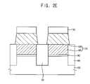
- a first dielectric layer 130 and a second dielectric layer 135 are successively formed on the second conductive layer pattern 120 of the floating gate 125 and the isolation layer 95 .
- the first dielectric layer 130 may be formed by depositing a metal silicon oxide (M x Si y O 2 ) on the isolation layer 95 to cover the second conductive layer pattern 120 .
- M x Si y O 2 metal silicon oxide
- x is about 0.75 and y is about 0.25.
- the first dielectric layer 130 may be formed by a CVD process or a PVD process.
- the first dielectric layer 130 is formed by a PECVD process, an ALD process, a sputtering process or a PLD process.
- the first dielectric layer 130 may have a thickness of about 30 ⁇ to 100 ⁇ measured from an upper face of the second conductive layer pattern 120 .
- the first dielectric layer 130 may include the metal silicon oxide such as a metal silicon oxide containing a transition metal in Group IV, a metal silicon oxide containing a transition metal in Group V or a metal silicon oxide containing a rare earth metal.
- the transition metal in Group IV may include titanium (Ti), zirconium (Zr) or hafnium (Hf).
- the transition metal in Group V may include vanadium (V), niobium (Nb) or tantalum (Ta).
- the rare earth metal may include scandium (Sc), yttrium (Y) or lanthanum (La).
- the first dielectric layer 130 includes a hafnium silicon oxide (Hf x Si y O 2 ).
- the second dielectric layer 135 may be formed on the first dielectric layer 130 by converting the metal silicon oxide in an upper portion of the first dielectric layer 130 into a metal silicon oxynitride (M x Si y O 2-z N z ).
- M x Si y O 2-z N z metal silicon oxynitride
- 0 ⁇ x ⁇ 1, 0 ⁇ y ⁇ 1, x+y 1 and 0 ⁇ z ⁇ 1.
- the second dielectric layer 135 may be formed by treating the upper portion of the first dielectric layer 130 using a plasma.
- the plasma may include ammonia (NH 3 ) plasma or nitrogen (N 2 ) plasma.
- the second dielectric layer 135 may include a metal silicon oxynitride generated from the metal silicon oxide in the first dielectric layer 130 .
- the first dielectric layer 130 may be treated at a temperature of about 300° C. to about 900° C. for about 60 seconds to about 180 seconds by applying a power of about 250 W to about 800 W. Since the first dielectric layer 130 contains the metal silicon oxide including the transition metal or the rare earth metal, the second dielectric layer 135 also contains the metal silicon oxynitride including a transition metal in Group IV, a transition metal in Group V or a rare earth metal.
- the second dielectric layer 135 includes titanium silicon oxynitride, zirconium silicon oxynitride, hafnium silicon oxynitride, a vanadium silicon oxynitride, niobium silicon oxynitride, tantalum silicon oxynitride, scandium silicon oxynitride, yttrium silicon oxynitride, lanthanum oxynitride, etc.
- the preliminary structure 140 may have a composition represented by [M x Si y O 2 /M x Si y O 2-z N z ]. That is, the preliminary dielectric structure 140 includes a metal a silicon oxide layer and a metal silicon oxynitride layer.
- the preliminary dielectric structure 140 including K (K is a positive integer) numbers of the first dielectric layers 130 and K numbers of the second dielectric layers 135 may be formed on the floating gate 125 and the isolation layer 95 . Since each of the first and the second dielectric layers 130 and 135 has a composition of M x Si y O 2 and a composition of M x Si y O 2-z N z , the preliminary dielectric structure 140 has an entire composition represented by [M x Si y O 2 /M x Si y O 2-z N z ] A .
- a wet etching process for removing a native oxide layer from on the semiconductor substrate 50 may be performed before the preliminary dielectric structure 140 is formed on the semiconductor 50 having the floating gate 125 and the isolation layer 95 .
- FIG. 3 is a graph illustrating capacitance variations of a single layer including hafnium silicon oxide and a double layer including hafnium silicon oxide/hafnium silicon oxynitride after thermal treatment processes.
- the capacitance variation is measured relative to an applied gate voltage.
- “ ⁇ ” represents the capacitance variation of the single layer including hafnium silicon oxide
- “ ⁇ ” indicates the capacitance variation of the double layer including hafnium silicon oxide/hafnium silicon oxynitride.
- FIG. 4 is a graph illustrating leakage current densities of a single layer including hafnium silicon oxide and a double layer including hafnium silicon oxide/hafnium silicon oxynitride after thermal treatment processes.
- the leakage current densities are measured relative to an applied gate voltage.
- ⁇ denotes the leakage current density of the single layer including hafnium silicon oxide
- ⁇ means the leakage current density of the double layer including hafnium silicon oxide/hafnium silicon oxynitride.
- the single layer and the double layer were formed by a first thermal treatment process at a temperature of about 750° C. and by a second thermal treatment process at a temperature of about 950° C. Since a typical dielectric layer of a non-volatile semiconductor memory device is thermally treated at a temperature of about 850° C. for about 20 minutes after the dielectric layer is formed on a typical floating gate, the capacitance variations and the leakage current densities of the single layer and the double layer were measured through the twice thermal treatment processes.
- the double layer including hafnium silicon oxide/hafnium silicon oxynitride has a capacitance higher than that of the single layer including hafnium silicon oxide. Additionally, the double layer including hafnium silicon oxide/hafnium silicon oxynitride has a leakage current density lower than that of the single layer including hafnium silicon oxide.
- a capacitance equivalent thickness (CET) of the double layer including hafnium silicon oxide/hafnium silicon oxynitride is about 24.1 ⁇
- a capacitance equivalent thickness (CET) of the single layer including hafnium silicon oxide is about 25.8 ⁇ .
- the double layer including hafnium silicon oxide/hafnium silicon oxynitride may have electrical characteristics considerably improved in comparison with those of the single layer including hafnium silicon oxide. Since hafnium silicon oxynitride has a thermal resistance superior to that of hafnium silicon oxide, the double layer including hafnium silicon oxide/hafnium silicon oxynitride may have a thermal resistance high than that of the single layer including hafnium silicon oxide.
- a third conductive layer 145 is formed on the preliminary dielectric structure 140 .
- the third conductive layer 145 may be formed using polysilicon doped in N + type impurities.
- the third conductive layer 145 may include polysilicon and a metal silicide.
- the metal silicide may include tungsten silicide (WSi x ), titanium silicide (TiSi x ), cobalt silicide (CoSi x ) or tantalum silicide (TaSi x ).
- the third conductive layer 145 and a preliminary dielectric structure 140 are sequentially etched using the third photoresist pattern as an etching mask.
- a dielectric structure 165 and a control gate 150 are formed on the floating gate 125 .
- the third conductive layer 145 , the second dielectric layer 135 and the first dielectric layer 130 are sequentially etched to thereby form a first dielectric layer pattern 160 , a second dielectric layer pattern 155 and a third conductive layer pattern 150 (i.e., the control gate 150 ) on the floating gate 125 .
- the first and the second dielectric layers 130 and 135 and the third conductive layer 145 may be etched by a dry etching process.
- a dielectric structure since a dielectric structure includes at least one metal silicon oxide layer and at least one metal silicon oxynitride layer, the dielectric structure may have a high dielectric constant and also have a good thermal resistance without thermal damage in a thermal treatment process.
- the non-volatile semiconductor memory device may also have good electrical characteristics such as a high capacitance and a low leakage current.
Abstract
Description
MxSiyO2 (1)
MxSiyO2-zNz (2)
[MxSiyO2/MxSiyO2-zNz]A (3)
Claims (7)
Applications Claiming Priority (2)
| Application Number | Priority Date | Filing Date | Title |
|---|---|---|---|
| KR10-2005-0006547 | 2005-01-25 | ||
| KR1020050006547A KR100623177B1 (en) | 2005-01-25 | 2005-01-25 | Dielectric structure having a high dielectric constant, method of forming the dielectric structure, non-volatile semiconductor memory device including the dielectric structure, and method of manufacturing the non-volatile semiconductor memory device |
Publications (2)
| Publication Number | Publication Date |
|---|---|
| US20060244147A1 US20060244147A1 (en) | 2006-11-02 |
| US7482677B2 true US7482677B2 (en) | 2009-01-27 |
Family
ID=37175282
Family Applications (1)
| Application Number | Title | Priority Date | Filing Date |
|---|---|---|---|
| US11/339,086 Active 2026-07-31 US7482677B2 (en) | 2005-01-25 | 2006-01-25 | Dielectric structures having high dielectric constants, and non-volatile semiconductor memory devices having the dielectric structures |
Country Status (2)
| Country | Link |
|---|---|
| US (1) | US7482677B2 (en) |
| KR (1) | KR100623177B1 (en) |
Cited By (33)
| Publication number | Priority date | Publication date | Assignee | Title |
|---|---|---|---|---|
| US8552771B1 (en) | 2012-05-29 | 2013-10-08 | Life Technologies Corporation | System for reducing noise in a chemical sensor array |
| US8692298B2 (en) | 2006-12-14 | 2014-04-08 | Life Technologies Corporation | Chemical sensor array having multiple sensors per well |
| US8731847B2 (en) | 2010-06-30 | 2014-05-20 | Life Technologies Corporation | Array configuration and readout scheme |
| US8742472B2 (en) | 2006-12-14 | 2014-06-03 | Life Technologies Corporation | Chemically sensitive sensors with sample and hold capacitors |
| US8841217B1 (en) | 2013-03-13 | 2014-09-23 | Life Technologies Corporation | Chemical sensor with protruded sensor surface |
| US8912580B2 (en) | 2009-05-29 | 2014-12-16 | Life Technologies Corporation | Active chemically-sensitive sensors with in-sensor current sources |
| US8912005B1 (en) | 2010-09-24 | 2014-12-16 | Life Technologies Corporation | Method and system for delta double sampling |
| US8963216B2 (en) | 2013-03-13 | 2015-02-24 | Life Technologies Corporation | Chemical sensor with sidewall spacer sensor surface |
| US8962366B2 (en) | 2013-01-28 | 2015-02-24 | Life Technologies Corporation | Self-aligned well structures for low-noise chemical sensors |
| US9116117B2 (en) | 2013-03-15 | 2015-08-25 | Life Technologies Corporation | Chemical sensor with sidewall sensor surface |
| US9128044B2 (en) | 2013-03-15 | 2015-09-08 | Life Technologies Corporation | Chemical sensors with consistent sensor surface areas |
| US9194000B2 (en) | 2008-06-25 | 2015-11-24 | Life Technologies Corporation | Methods and apparatus for measuring analytes using large scale FET arrays |
| US9239313B2 (en) | 2010-06-30 | 2016-01-19 | Life Technologies Corporation | Ion-sensing charge-accumulation circuits and methods |
| US9404920B2 (en) | 2006-12-14 | 2016-08-02 | Life Technologies Corporation | Methods and apparatus for detecting molecular interactions using FET arrays |
| US9618475B2 (en) | 2010-09-15 | 2017-04-11 | Life Technologies Corporation | Methods and apparatus for measuring analytes |
| US9671363B2 (en) | 2013-03-15 | 2017-06-06 | Life Technologies Corporation | Chemical sensor with consistent sensor surface areas |
| US9823217B2 (en) | 2013-03-15 | 2017-11-21 | Life Technologies Corporation | Chemical device with thin conductive element |
| US9835585B2 (en) | 2013-03-15 | 2017-12-05 | Life Technologies Corporation | Chemical sensor with protruded sensor surface |
| US9841398B2 (en) | 2013-01-08 | 2017-12-12 | Life Technologies Corporation | Methods for manufacturing well structures for low-noise chemical sensors |
| US9852919B2 (en) | 2013-01-04 | 2017-12-26 | Life Technologies Corporation | Methods and systems for point of use removal of sacrificial material |
| US9927393B2 (en) | 2009-05-29 | 2018-03-27 | Life Technologies Corporation | Methods and apparatus for measuring analytes |
| US9944981B2 (en) | 2008-10-22 | 2018-04-17 | Life Technologies Corporation | Methods and apparatus for measuring analytes |
| US9960253B2 (en) | 2010-07-03 | 2018-05-01 | Life Technologies Corporation | Chemically sensitive sensor with lightly doped drains |
| US9970984B2 (en) | 2011-12-01 | 2018-05-15 | Life Technologies Corporation | Method and apparatus for identifying defects in a chemical sensor array |
| US10077472B2 (en) | 2014-12-18 | 2018-09-18 | Life Technologies Corporation | High data rate integrated circuit with power management |
| US10100357B2 (en) | 2013-05-09 | 2018-10-16 | Life Technologies Corporation | Windowed sequencing |
| US10379079B2 (en) | 2014-12-18 | 2019-08-13 | Life Technologies Corporation | Methods and apparatus for measuring analytes using large scale FET arrays |
| US10451585B2 (en) | 2009-05-29 | 2019-10-22 | Life Technologies Corporation | Methods and apparatus for measuring analytes |
| US10458942B2 (en) | 2013-06-10 | 2019-10-29 | Life Technologies Corporation | Chemical sensor array having multiple sensors per well |
| US10605767B2 (en) | 2014-12-18 | 2020-03-31 | Life Technologies Corporation | High data rate integrated circuit with transmitter configuration |
| US11231451B2 (en) | 2010-06-30 | 2022-01-25 | Life Technologies Corporation | Methods and apparatus for testing ISFET arrays |
| US11307166B2 (en) | 2010-07-01 | 2022-04-19 | Life Technologies Corporation | Column ADC |
| US11339430B2 (en) | 2007-07-10 | 2022-05-24 | Life Technologies Corporation | Methods and apparatus for measuring analytes using large scale FET arrays |
Families Citing this family (7)
| Publication number | Priority date | Publication date | Assignee | Title |
|---|---|---|---|---|
| US8536661B1 (en) | 2004-06-25 | 2013-09-17 | University Of Hawaii | Biosensor chip sensor protection methods |
| TW200816282A (en) * | 2006-09-27 | 2008-04-01 | Promos Technologies Inc | Method for reducing stress between a conductive layer and a mask layer and use of the same |
| US8673627B2 (en) | 2009-05-29 | 2014-03-18 | Life Technologies Corporation | Apparatus and methods for performing electrochemical reactions |
| JP5732827B2 (en) | 2010-02-09 | 2015-06-10 | ソニー株式会社 | Storage element, storage device, and operation method of storage device |
| JP2013016530A (en) * | 2011-06-30 | 2013-01-24 | Sony Corp | Memory element, method for manufacturing the same, and memory device |
| US8747748B2 (en) | 2012-01-19 | 2014-06-10 | Life Technologies Corporation | Chemical sensor with conductive cup-shaped sensor surface |
| US8821798B2 (en) | 2012-01-19 | 2014-09-02 | Life Technologies Corporation | Titanium nitride as sensing layer for microwell structure |
Citations (12)
| Publication number | Priority date | Publication date | Assignee | Title |
|---|---|---|---|---|
| US5057448A (en) * | 1988-02-26 | 1991-10-15 | Hitachi, Ltd. | Method of making a semiconductor device having DRAM cells and floating gate memory cells |
| KR19980032692A (en) | 1996-10-10 | 1998-07-25 | 알.제이.보토스 | Floating gate memory device and its memory device manufacturing process |
| KR19990077767A (en) | 1998-03-12 | 1999-10-25 | 루센트 테크놀러지스 인크 | Electronic Components With Doped Metal Oxide Dielectric Materials And A Process For Making Electronic Components With Doped Metal Oxide Dielectric Materials |
| US20030141536A1 (en) * | 2000-04-06 | 2003-07-31 | Weimer Ronald A. | Integrated circuit with a dielectric layer exposed to a hydrogen-bearing nitrogen source |
| US20040046197A1 (en) * | 2002-05-16 | 2004-03-11 | Cem Basceri | MIS capacitor and method of formation |
| KR20040057535A (en) | 2002-12-26 | 2004-07-02 | 주식회사 하이닉스반도체 | Method of manufacturing a semiconductor device |
| KR20040072051A (en) | 2003-02-07 | 2004-08-16 | 가부시끼가이샤 도시바 | Semiconductor device and method for manufacturing the same |
| US6783997B2 (en) * | 2001-12-19 | 2004-08-31 | Texas Instruments Incorporated | Gate structure and method |
| US6797567B2 (en) | 2002-12-24 | 2004-09-28 | Macronix International Co., Ltd. | High-K tunneling dielectric for read only memory device and fabrication method thereof |
| US20040195094A1 (en) * | 2002-08-06 | 2004-10-07 | Shuichi Irumata | Hafnium silicide target and manufacturing method for preparation thereof |
| US20040201058A1 (en) * | 2003-04-11 | 2004-10-14 | Masahisa Sonoda | Nonvolatile semiconductor memory device having grooves isolating the floating electrodes of memory cells and method of manufacturing the nonvolatile semiconductor memory device |
| US20050046007A1 (en) * | 2003-08-25 | 2005-03-03 | Casio Computer Co., Ltd. | Junction substrate and method of bonding substrates together |
Family Cites Families (6)
| Publication number | Priority date | Publication date | Assignee | Title |
|---|---|---|---|---|
| JP4342621B2 (en) * | 1998-12-09 | 2009-10-14 | 株式会社東芝 | Nonvolatile semiconductor memory device |
| KR100760078B1 (en) * | 2000-03-13 | 2007-09-18 | 다다히로 오미 | Method for forming dielectric film |
| KR100359489B1 (en) * | 2000-11-07 | 2002-11-04 | 광주과학기술원 | Method of fabricating gate dielectric for use in semiconductor device |
| JP3987418B2 (en) * | 2002-11-15 | 2007-10-10 | 株式会社東芝 | Semiconductor memory device |
| KR100973281B1 (en) * | 2003-06-10 | 2010-07-30 | 삼성전자주식회사 | SONOS memory device and method of manufacturing the same |
| KR100604846B1 (en) * | 2004-04-23 | 2006-07-31 | 삼성전자주식회사 | Memory Device with Dielectric Multilayer and Method of Manufacturing the same |
-
2005
- 2005-01-25 KR KR1020050006547A patent/KR100623177B1/en active IP Right Grant
-
2006
- 2006-01-25 US US11/339,086 patent/US7482677B2/en active Active
Patent Citations (12)
| Publication number | Priority date | Publication date | Assignee | Title |
|---|---|---|---|---|
| US5057448A (en) * | 1988-02-26 | 1991-10-15 | Hitachi, Ltd. | Method of making a semiconductor device having DRAM cells and floating gate memory cells |
| KR19980032692A (en) | 1996-10-10 | 1998-07-25 | 알.제이.보토스 | Floating gate memory device and its memory device manufacturing process |
| KR19990077767A (en) | 1998-03-12 | 1999-10-25 | 루센트 테크놀러지스 인크 | Electronic Components With Doped Metal Oxide Dielectric Materials And A Process For Making Electronic Components With Doped Metal Oxide Dielectric Materials |
| US20030141536A1 (en) * | 2000-04-06 | 2003-07-31 | Weimer Ronald A. | Integrated circuit with a dielectric layer exposed to a hydrogen-bearing nitrogen source |
| US6783997B2 (en) * | 2001-12-19 | 2004-08-31 | Texas Instruments Incorporated | Gate structure and method |
| US20040046197A1 (en) * | 2002-05-16 | 2004-03-11 | Cem Basceri | MIS capacitor and method of formation |
| US20040195094A1 (en) * | 2002-08-06 | 2004-10-07 | Shuichi Irumata | Hafnium silicide target and manufacturing method for preparation thereof |
| US6797567B2 (en) | 2002-12-24 | 2004-09-28 | Macronix International Co., Ltd. | High-K tunneling dielectric for read only memory device and fabrication method thereof |
| KR20040057535A (en) | 2002-12-26 | 2004-07-02 | 주식회사 하이닉스반도체 | Method of manufacturing a semiconductor device |
| KR20040072051A (en) | 2003-02-07 | 2004-08-16 | 가부시끼가이샤 도시바 | Semiconductor device and method for manufacturing the same |
| US20040201058A1 (en) * | 2003-04-11 | 2004-10-14 | Masahisa Sonoda | Nonvolatile semiconductor memory device having grooves isolating the floating electrodes of memory cells and method of manufacturing the nonvolatile semiconductor memory device |
| US20050046007A1 (en) * | 2003-08-25 | 2005-03-03 | Casio Computer Co., Ltd. | Junction substrate and method of bonding substrates together |
Non-Patent Citations (1)
| Title |
|---|
| Wilk et al., Electrical porperties of hafnium silicate gate dielectrics deposited directly on silicon, May 10, 1999, Applied Physics Letters, vol. 74 No. 19, pp. 2854-2856. * |
Cited By (81)
| Publication number | Priority date | Publication date | Assignee | Title |
|---|---|---|---|---|
| US10816506B2 (en) | 2006-12-14 | 2020-10-27 | Life Technologies Corporation | Method for measuring analytes using large scale chemfet arrays |
| US10502708B2 (en) | 2006-12-14 | 2019-12-10 | Life Technologies Corporation | Chemically-sensitive sensor array calibration circuitry |
| US9951382B2 (en) | 2006-12-14 | 2018-04-24 | Life Technologies Corporation | Methods and apparatus for measuring analytes using large scale FET arrays |
| US9023189B2 (en) | 2006-12-14 | 2015-05-05 | Life Technologies Corporation | High density sensor array without wells |
| US11732297B2 (en) * | 2006-12-14 | 2023-08-22 | Life Technologies Corporation | Methods and apparatus for measuring analytes using large scale FET arrays |
| US8742472B2 (en) | 2006-12-14 | 2014-06-03 | Life Technologies Corporation | Chemically sensitive sensors with sample and hold capacitors |
| US9989489B2 (en) | 2006-12-14 | 2018-06-05 | Life Technnologies Corporation | Methods for calibrating an array of chemically-sensitive sensors |
| US10203300B2 (en) | 2006-12-14 | 2019-02-12 | Life Technologies Corporation | Methods and apparatus for measuring analytes using large scale FET arrays |
| US20220340965A1 (en) * | 2006-12-14 | 2022-10-27 | Life Technologies Corporation | Methods and Apparatus for Measuring Analytes Using Large Scale FET Arrays |
| US8890216B2 (en) | 2006-12-14 | 2014-11-18 | Life Technologies Corporation | Methods and apparatus for measuring analytes using large scale FET arrays |
| US10415079B2 (en) | 2006-12-14 | 2019-09-17 | Life Technologies Corporation | Methods and apparatus for detecting molecular interactions using FET arrays |
| US9404920B2 (en) | 2006-12-14 | 2016-08-02 | Life Technologies Corporation | Methods and apparatus for detecting molecular interactions using FET arrays |
| US11435314B2 (en) | 2006-12-14 | 2022-09-06 | Life Technologies Corporation | Chemically-sensitive sensor array device |
| US9269708B2 (en) | 2006-12-14 | 2016-02-23 | Life Technologies Corporation | Methods and apparatus for measuring analytes using large scale FET arrays |
| US8692298B2 (en) | 2006-12-14 | 2014-04-08 | Life Technologies Corporation | Chemical sensor array having multiple sensors per well |
| US10633699B2 (en) | 2006-12-14 | 2020-04-28 | Life Technologies Corporation | Methods and apparatus for measuring analytes using large scale FET arrays |
| US8766328B2 (en) | 2006-12-14 | 2014-07-01 | Life Technologies Corporation | Chemically-sensitive sample and hold sensors |
| US9134269B2 (en) | 2006-12-14 | 2015-09-15 | Life Technologies Corporation | Methods and apparatus for measuring analytes using large scale FET arrays |
| US11339430B2 (en) | 2007-07-10 | 2022-05-24 | Life Technologies Corporation | Methods and apparatus for measuring analytes using large scale FET arrays |
| US9194000B2 (en) | 2008-06-25 | 2015-11-24 | Life Technologies Corporation | Methods and apparatus for measuring analytes using large scale FET arrays |
| US11448613B2 (en) | 2008-10-22 | 2022-09-20 | Life Technologies Corporation | ChemFET sensor array including overlying array of wells |
| US9964515B2 (en) | 2008-10-22 | 2018-05-08 | Life Technologies Corporation | Integrated sensor arrays for biological and chemical analysis |
| US9944981B2 (en) | 2008-10-22 | 2018-04-17 | Life Technologies Corporation | Methods and apparatus for measuring analytes |
| US11874250B2 (en) | 2008-10-22 | 2024-01-16 | Life Technologies Corporation | Integrated sensor arrays for biological and chemical analysis |
| US11137369B2 (en) | 2008-10-22 | 2021-10-05 | Life Technologies Corporation | Integrated sensor arrays for biological and chemical analysis |
| US10718733B2 (en) | 2009-05-29 | 2020-07-21 | Life Technologies Corporation | Methods and apparatus for measuring analytes |
| US10451585B2 (en) | 2009-05-29 | 2019-10-22 | Life Technologies Corporation | Methods and apparatus for measuring analytes |
| US10809226B2 (en) | 2009-05-29 | 2020-10-20 | Life Technologies Corporation | Methods and apparatus for measuring analytes |
| US8912580B2 (en) | 2009-05-29 | 2014-12-16 | Life Technologies Corporation | Active chemically-sensitive sensors with in-sensor current sources |
| US11692964B2 (en) | 2009-05-29 | 2023-07-04 | Life Technologies Corporation | Methods and apparatus for measuring analytes |
| US9927393B2 (en) | 2009-05-29 | 2018-03-27 | Life Technologies Corporation | Methods and apparatus for measuring analytes |
| US11768171B2 (en) | 2009-05-29 | 2023-09-26 | Life Technologies Corporation | Methods and apparatus for measuring analytes |
| US10641729B2 (en) | 2010-06-30 | 2020-05-05 | Life Technologies Corporation | Column ADC |
| US9164070B2 (en) | 2010-06-30 | 2015-10-20 | Life Technologies Corporation | Column adc |
| US8731847B2 (en) | 2010-06-30 | 2014-05-20 | Life Technologies Corporation | Array configuration and readout scheme |
| US10481123B2 (en) | 2010-06-30 | 2019-11-19 | Life Technologies Corporation | Ion-sensing charge-accumulation circuits and methods |
| US8742471B2 (en) | 2010-06-30 | 2014-06-03 | Life Technologies Corporation | Chemical sensor array with leakage compensation circuit |
| US8741680B2 (en) | 2010-06-30 | 2014-06-03 | Life Technologies Corporation | Two-transistor pixel array |
| US9239313B2 (en) | 2010-06-30 | 2016-01-19 | Life Technologies Corporation | Ion-sensing charge-accumulation circuits and methods |
| US11231451B2 (en) | 2010-06-30 | 2022-01-25 | Life Technologies Corporation | Methods and apparatus for testing ISFET arrays |
| US8983783B2 (en) | 2010-06-30 | 2015-03-17 | Life Technologies Corporation | Chemical detection device having multiple flow channels |
| US11307166B2 (en) | 2010-07-01 | 2022-04-19 | Life Technologies Corporation | Column ADC |
| US9960253B2 (en) | 2010-07-03 | 2018-05-01 | Life Technologies Corporation | Chemically sensitive sensor with lightly doped drains |
| US9958414B2 (en) | 2010-09-15 | 2018-05-01 | Life Technologies Corporation | Apparatus for measuring analytes including chemical sensor array |
| US9618475B2 (en) | 2010-09-15 | 2017-04-11 | Life Technologies Corporation | Methods and apparatus for measuring analytes |
| US9110015B2 (en) | 2010-09-24 | 2015-08-18 | Life Technologies Corporation | Method and system for delta double sampling |
| US8912005B1 (en) | 2010-09-24 | 2014-12-16 | Life Technologies Corporation | Method and system for delta double sampling |
| US10365321B2 (en) | 2011-12-01 | 2019-07-30 | Life Technologies Corporation | Method and apparatus for identifying defects in a chemical sensor array |
| US10598723B2 (en) | 2011-12-01 | 2020-03-24 | Life Technologies Corporation | Method and apparatus for identifying defects in a chemical sensor array |
| US9970984B2 (en) | 2011-12-01 | 2018-05-15 | Life Technologies Corporation | Method and apparatus for identifying defects in a chemical sensor array |
| US9985624B2 (en) | 2012-05-29 | 2018-05-29 | Life Technologies Corporation | System for reducing noise in a chemical sensor array |
| US8552771B1 (en) | 2012-05-29 | 2013-10-08 | Life Technologies Corporation | System for reducing noise in a chemical sensor array |
| US8786331B2 (en) | 2012-05-29 | 2014-07-22 | Life Technologies Corporation | System for reducing noise in a chemical sensor array |
| US10404249B2 (en) | 2012-05-29 | 2019-09-03 | Life Technologies Corporation | System for reducing noise in a chemical sensor array |
| US9270264B2 (en) | 2012-05-29 | 2016-02-23 | Life Technologies Corporation | System for reducing noise in a chemical sensor array |
| US9852919B2 (en) | 2013-01-04 | 2017-12-26 | Life Technologies Corporation | Methods and systems for point of use removal of sacrificial material |
| US9841398B2 (en) | 2013-01-08 | 2017-12-12 | Life Technologies Corporation | Methods for manufacturing well structures for low-noise chemical sensors |
| US10436742B2 (en) | 2013-01-08 | 2019-10-08 | Life Technologies Corporation | Methods for manufacturing well structures for low-noise chemical sensors |
| US8962366B2 (en) | 2013-01-28 | 2015-02-24 | Life Technologies Corporation | Self-aligned well structures for low-noise chemical sensors |
| US9995708B2 (en) | 2013-03-13 | 2018-06-12 | Life Technologies Corporation | Chemical sensor with sidewall spacer sensor surface |
| US8841217B1 (en) | 2013-03-13 | 2014-09-23 | Life Technologies Corporation | Chemical sensor with protruded sensor surface |
| US8963216B2 (en) | 2013-03-13 | 2015-02-24 | Life Technologies Corporation | Chemical sensor with sidewall spacer sensor surface |
| US9823217B2 (en) | 2013-03-15 | 2017-11-21 | Life Technologies Corporation | Chemical device with thin conductive element |
| US10481124B2 (en) | 2013-03-15 | 2019-11-19 | Life Technologies Corporation | Chemical device with thin conductive element |
| US10422767B2 (en) | 2013-03-15 | 2019-09-24 | Life Technologies Corporation | Chemical sensor with consistent sensor surface areas |
| US9671363B2 (en) | 2013-03-15 | 2017-06-06 | Life Technologies Corporation | Chemical sensor with consistent sensor surface areas |
| US9128044B2 (en) | 2013-03-15 | 2015-09-08 | Life Technologies Corporation | Chemical sensors with consistent sensor surface areas |
| US9116117B2 (en) | 2013-03-15 | 2015-08-25 | Life Technologies Corporation | Chemical sensor with sidewall sensor surface |
| US9835585B2 (en) | 2013-03-15 | 2017-12-05 | Life Technologies Corporation | Chemical sensor with protruded sensor surface |
| US10100357B2 (en) | 2013-05-09 | 2018-10-16 | Life Technologies Corporation | Windowed sequencing |
| US10655175B2 (en) | 2013-05-09 | 2020-05-19 | Life Technologies Corporation | Windowed sequencing |
| US11028438B2 (en) | 2013-05-09 | 2021-06-08 | Life Technologies Corporation | Windowed sequencing |
| US11774401B2 (en) | 2013-06-10 | 2023-10-03 | Life Technologies Corporation | Chemical sensor array having multiple sensors per well |
| US10816504B2 (en) | 2013-06-10 | 2020-10-27 | Life Technologies Corporation | Chemical sensor array having multiple sensors per well |
| US11499938B2 (en) | 2013-06-10 | 2022-11-15 | Life Technologies Corporation | Chemical sensor array having multiple sensors per well |
| US10458942B2 (en) | 2013-06-10 | 2019-10-29 | Life Technologies Corporation | Chemical sensor array having multiple sensors per well |
| US10077472B2 (en) | 2014-12-18 | 2018-09-18 | Life Technologies Corporation | High data rate integrated circuit with power management |
| US11536688B2 (en) | 2014-12-18 | 2022-12-27 | Life Technologies Corporation | High data rate integrated circuit with transmitter configuration |
| US10605767B2 (en) | 2014-12-18 | 2020-03-31 | Life Technologies Corporation | High data rate integrated circuit with transmitter configuration |
| US10767224B2 (en) | 2014-12-18 | 2020-09-08 | Life Technologies Corporation | High data rate integrated circuit with power management |
| US10379079B2 (en) | 2014-12-18 | 2019-08-13 | Life Technologies Corporation | Methods and apparatus for measuring analytes using large scale FET arrays |
Also Published As
| Publication number | Publication date |
|---|---|
| KR20060085735A (en) | 2006-07-28 |
| KR100623177B1 (en) | 2006-09-13 |
| US20060244147A1 (en) | 2006-11-02 |
Similar Documents
| Publication | Publication Date | Title |
|---|---|---|
| US7482677B2 (en) | Dielectric structures having high dielectric constants, and non-volatile semiconductor memory devices having the dielectric structures | |
| US7419918B2 (en) | Methods of forming a thin-film structure, methods of manufacturing non-volatile semiconductor devices using the same, and resulting non-volatile semiconductor devices | |
| US7648874B2 (en) | Method of forming a dielectric structure having a high dielectric constant and method of manufacturing a semiconductor device having the dielectric structure | |
| US6927145B1 (en) | Bitline hard mask spacer flow for memory cell scaling | |
| US6998667B2 (en) | Scalable gate and storage dielectric | |
| US20070120179A1 (en) | SONOS type non-volatile memory devices having a laminate blocking insulation layer and methods of manufacturing the same | |
| US7427533B2 (en) | Methods of fabricating semiconductor devices including trench device isolation layers having protective insulating layers and related devices | |
| US8329598B2 (en) | Sacrificial nitride and gate replacement | |
| US8481387B2 (en) | Method of forming an insulation structure and method of manufacturing a semiconductor device using the same | |
| US7018868B1 (en) | Disposable hard mask for memory bitline scaling | |
| US7727893B2 (en) | Method of forming a dielectric layer pattern and method of manufacturing a non-volatile memory device using the same | |
| US7902059B2 (en) | Methods of forming void-free layers in openings of semiconductor substrates | |
| US8049269B2 (en) | Non-volatile memory device and method of manufacturing the same | |
| US20140080298A1 (en) | Non-volatile memory devices and methods of manufacturing the same | |
| US8270216B2 (en) | Semiconductor storage device and method of manufacturing the same | |
| US20050266640A1 (en) | Method of forming a dielectric layer and method of manufacturing a nonvolatile memory device using the same | |
| US20090039405A1 (en) | Oro and orpro with bit line trench to suppress transport program disturb | |
| US20070176225A1 (en) | Semiconductor device and method of manufacturing the same | |
| US7402491B2 (en) | Methods of manufacturing a semiconductor device including a dielectric layer including zirconium | |
| US7585787B2 (en) | Semiconductor memory device and method of manufacturing the same | |
| US6316316B1 (en) | Method of forming high density and low power flash memories with a high capacitive-coupling ratio | |
| US7498222B1 (en) | Enhanced etching of a high dielectric constant layer | |
| US20090101963A1 (en) | Split charge storage node inner spacer process | |
| US7867849B2 (en) | Method of manufacturing a non-volatile semiconductor device | |
| US20060138523A1 (en) | Semiconductor memory device and method of manufacturing the semiconductor memory device |
Legal Events
| Date | Code | Title | Description |
|---|---|---|---|
| AS | Assignment |
Owner name: SAMSUNG ELECTRONICS CO., LTD., KOREA, REPUBLIC OF Free format text: ASSIGNMENT OF ASSIGNORS INTEREST;ASSIGNORS:LEE, JONG-CHEOL;KIM, SUNG-TAE;KIM, YOUNG-SUN;AND OTHERS;REEL/FRAME:017879/0009;SIGNING DATES FROM 20060323 TO 20060630 |
|
| STCF | Information on status: patent grant |
Free format text: PATENTED CASE |
|
| FPAY | Fee payment |
Year of fee payment: 4 |
|
| FPAY | Fee payment |
Year of fee payment: 8 |
|
| MAFP | Maintenance fee payment |
Free format text: PAYMENT OF MAINTENANCE FEE, 12TH YEAR, LARGE ENTITY (ORIGINAL EVENT CODE: M1553); ENTITY STATUS OF PATENT OWNER: LARGE ENTITY Year of fee payment: 12 |