US7473959B2 - Non-volatile semiconductor memory devices and methods of fabricating the same - Google Patents

Non-volatile semiconductor memory devices and methods of fabricating the same Download PDF

Info

Publication number
US7473959B2
US7473959B2 US11/601,505 US60150506A US7473959B2 US 7473959 B2 US7473959 B2 US 7473959B2 US 60150506 A US60150506 A US 60150506A US 7473959 B2 US7473959 B2 US 7473959B2
Authority
US
United States
Prior art keywords
insulation film
charge
film
barrier
layer
Prior art date
Legal status (The legal status is an assumption and is not a legal conclusion. Google has not performed a legal analysis and makes no representation as to the accuracy of the status listed.)
Active, expires
Application number
US11/601,505
Other versions
US20070063265A1 (en
Inventor
Sung-Hae Lee
Chang-Hyun Lee
Ki-Hyun Hwang
Sung-Kweon Baek
Kwang-Min Park
Current Assignee (The listed assignees may be inaccurate. Google has not performed a legal analysis and makes no representation or warranty as to the accuracy of the list.)
Samsung Electronics Co Ltd
Original Assignee
Samsung Electronics Co Ltd
Priority date (The priority date is an assumption and is not a legal conclusion. Google has not performed a legal analysis and makes no representation as to the accuracy of the date listed.)
Filing date
Publication date
Priority claimed from KR10-2002-0005622A external-priority patent/KR100456580B1/en
Priority claimed from US11/043,485 external-priority patent/US7400009B2/en
Priority claimed from KR1020060047231A external-priority patent/KR100794655B1/en
Application filed by Samsung Electronics Co Ltd filed Critical Samsung Electronics Co Ltd
Priority to US11/601,505 priority Critical patent/US7473959B2/en
Assigned to SAMSUNG ELECTRONICS CO., LTD. reassignment SAMSUNG ELECTRONICS CO., LTD. ASSIGNMENT OF ASSIGNORS INTEREST (SEE DOCUMENT FOR DETAILS). Assignors: BAEK, SUNG-KWEON, HWANG, KI-HYUN, LEE, CHUNG-HYUN, LEE, SUNG-HAE, PARK, KWANG-MIN
Assigned to SAMSUNG ELECTRONICS CO., LTD. reassignment SAMSUNG ELECTRONICS CO., LTD. RE-RECORD TO CORRECT THE NAME OF THE SECOND ASSIGNOR, PREVIOUSLY RECORDED ON REEL 018617 FRAME 0173. Assignors: BAEK, SUNG-KWEON, HWANG, KI-HYUN, LEE, CHANG-HYUN, LEE, SUNG-HAE, PARK, KWANG-MIN
Publication of US20070063265A1 publication Critical patent/US20070063265A1/en
Application granted granted Critical
Publication of US7473959B2 publication Critical patent/US7473959B2/en
Active legal-status Critical Current
Adjusted expiration legal-status Critical

Links

Images

Classifications

    • HELECTRICITY
    • H01ELECTRIC ELEMENTS
    • H01LSEMICONDUCTOR DEVICES NOT COVERED BY CLASS H10
    • H01L29/00Semiconductor devices adapted for rectifying, amplifying, oscillating or switching, or capacitors or resistors with at least one potential-jump barrier or surface barrier, e.g. PN junction depletion layer or carrier concentration layer; Details of semiconductor bodies or of electrodes thereof  ; Multistep manufacturing processes therefor
    • H01L29/66Types of semiconductor device ; Multistep manufacturing processes therefor
    • H01L29/68Types of semiconductor device ; Multistep manufacturing processes therefor controllable by only the electric current supplied, or only the electric potential applied, to an electrode which does not carry the current to be rectified, amplified or switched
    • H01L29/76Unipolar devices, e.g. field effect transistors
    • H01L29/772Field effect transistors
    • H01L29/78Field effect transistors with field effect produced by an insulated gate
    • H01L29/792Field effect transistors with field effect produced by an insulated gate with charge trapping gate insulator, e.g. MNOS-memory transistors
    • HELECTRICITY
    • H01ELECTRIC ELEMENTS
    • H01LSEMICONDUCTOR DEVICES NOT COVERED BY CLASS H10
    • H01L29/00Semiconductor devices adapted for rectifying, amplifying, oscillating or switching, or capacitors or resistors with at least one potential-jump barrier or surface barrier, e.g. PN junction depletion layer or carrier concentration layer; Details of semiconductor bodies or of electrodes thereof  ; Multistep manufacturing processes therefor
    • H01L29/40Electrodes ; Multistep manufacturing processes therefor
    • H01L29/43Electrodes ; Multistep manufacturing processes therefor characterised by the materials of which they are formed
    • H01L29/49Metal-insulator-semiconductor electrodes, e.g. gates of MOSFET
    • H01L29/51Insulating materials associated therewith
    • H01L29/511Insulating materials associated therewith with a compositional variation, e.g. multilayer structures
    • H01L29/513Insulating materials associated therewith with a compositional variation, e.g. multilayer structures the variation being perpendicular to the channel plane
    • HELECTRICITY
    • H10SEMICONDUCTOR DEVICES; ELECTRIC SOLID-STATE DEVICES NOT OTHERWISE PROVIDED FOR
    • H10BELECTRONIC MEMORY DEVICES
    • H10B43/00EEPROM devices comprising charge-trapping gate insulators
    • H10B43/10EEPROM devices comprising charge-trapping gate insulators characterised by the top-view layout
    • HELECTRICITY
    • H10SEMICONDUCTOR DEVICES; ELECTRIC SOLID-STATE DEVICES NOT OTHERWISE PROVIDED FOR
    • H10BELECTRONIC MEMORY DEVICES
    • H10B69/00Erasable-and-programmable ROM [EPROM] devices not provided for in groups H10B41/00 - H10B63/00, e.g. ultraviolet erasable-and-programmable ROM [UVEPROM] devices

Definitions

  • the present invention relates to non-volatile memory devices and methods of fabricating nonvolatile memory devices.
  • a floating gate type memory device may include a control gate and a conductive floating gate that is isolated, by an insulating layer, from a substrate channel.
  • Floating gate type memory devices may be programmed by storing charges as free carriers on the conductive floating gate.
  • Floating trap type memory devices may include a non-conductive charge storage layer between a gate electrode and a substrate. Floating trap type memory devices may be programmed by storing charges in traps in the non-conductive charge storage layer.
  • Floating gate type memory devices generally have a thicker tunneling insulating layer than floating trap type memory devices to provide comparable reliability for storing charges.
  • a thicker tunneling insulating layer may result in an increased operating voltage for the memory device and an increased complexity of associated peripheral circuitry. Consequently, it may be more difficult to provide high integration density and low power consumption for floating gate type memory devices than for floating trap type memory devices.
  • FIG. 1 A SONOS (silicon-oxide-nitride-oxide-semiconductor) structure of a conventional floating trap type unit memory device is shown in FIG. 1 .
  • the memory device includes a tunneling insulating layer 20 , a charge storage layer 22 , a blocking insulating layer 24 , and a gate electrode 27 that are sequentially stacked on an active region of a P-type semiconductor substrate 10 .
  • An N + type impurity diffusion layer 28 is formed at an active region on opposite sides of the gate electrode 27 .
  • the tunneling insulating layer 20 may include a thermal oxide material and the charge storage layer 22 may include silicon nitride material.
  • FIG. 2 An energy band diagram of a floating trap type unit memory device is shown in FIG. 2 , taken along a line I-I′ of FIG. 1 .
  • Intrinsic energy band gaps are shown for the materials corresponding to the semiconductor substrate 10 , the tunneling insulating layer 20 , the charge storage layer 22 , the blocking insulating layer 24 , and the gate electrode 27 . Differences between the energy band gaps may result in potential barriers at the interfaces between the materials.
  • the charge storage layer 22 can include silicon nitride which has an energy band gap of about 5 eV.
  • the corresponding potential barriers between the tunneling insulating layer 20 and the charge storage layer 22 may be about 1 eV and 2 eV, respectively, for the conduction band and the valence band.
  • a silicon nitride layer is known to have three trap levels.
  • a trap center of the silicon nitride layer includes a silicon atom that combines with three nitrogen atoms 20 and has one dangling bond.
  • the state When no electron combines with the dangling bond (i.e., a hole combines therewith), the state may be called a first trap level E 1 .
  • the state When one electron combines with the dangling bond, the state may be called a second trap level E 2 , which is higher than the first trap level E 1 .
  • the state When two electrons combine with the dangling bond, the state may be called a third trap level E 3 , which is higher than the second trap level E 2 .
  • a floating trap type non-volatile memory device uses trap levels, such as those found in a silicon nitride layer, for memory operations.
  • trap levels such as those found in a silicon nitride layer
  • When a positive voltage is applied on the gate electrode 27 electrons are tunneled via the tunneling insulating layer 20 to become trapped in the charge storage layer 22 .
  • a threshold voltage of the memory device is increased, and the memory device becomes programmed.
  • the quantity of charges from the channel should be relatively greater than the quantity of charges from the gate electrode. For example, when a positive voltage is applied to the gate electrode, if the quantity of holes provided from the gate electrode to the floating trap is equal to the quantity of electrons provided from the channel to the floating trap, negative charges are offset by positive charges and vice versa. Accordingly, the threshold voltage is not changed and programming may be precluded.
  • the thickness of the silicon oxide layer serving as a tunneling oxide layer
  • current flow from direct tunneling may exceed current flow from F-N tunneling and an erase operation may occur.
  • a blocking oxide layer has a thickness of about 50 ⁇
  • charge may be primarily moved by F-N tunneling and the quantity of charges from the channel may be greater than the quantity of charges from the gate electrode.
  • the thickness of the tunneling insulating layer is 20 ⁇ or less and the blocking insulating layer is thicker than the tunneling insulating layer, charges may be primarily provided from the channel in erase and program operations, and the threshold voltage may be more easily controlled.
  • the thickness of the silicon oxide layer may affect the data retention time of the memory device. For example, when the thickness of the silicon oxide layer is 20 ⁇ or less, charges stored in the floating trap may leak more easily and the data retention time of the memory device may be shortened. When the thickness of the silicon oxide layer is 20 ⁇ or higher, the data retention time may be increased but the primary flow of charges to the floating trap may be by F-N tunneling. F-N tunneling may be more easily carried out as the effective mass of charge carriers becomes smaller and the electric field on the charge carrier path becomes stronger.
  • the symbols “ot”, “ob”, and “SIN” represent the tunneling insulating layer, the blocking insulating layer, and the silicon nitride layer, respectively.
  • the symbol “E” represents the electric field
  • “Vg” represents the voltage of a gate electrode
  • “ ⁇ ms” represents a difference of a work function between the substrate and the gate electrode
  • “ ⁇ b” represents a substrate surface potential
  • “X” represents a thickness of the oxide layer
  • “ ⁇ ” represents a dielectric constant.
  • E ⁇ ⁇ ot Vg - ⁇ ⁇ ⁇ m ⁇ ⁇ s - ⁇ ⁇ ⁇ b - Q ⁇ ( X ⁇ ⁇ ot ⁇ ⁇ ( ob ) + X ⁇ ⁇ n 2 ⁇ ⁇ ⁇ ( n ) ) X ⁇ ⁇ ot + X ⁇ ⁇ n ⁇ ⁇ ⁇ ( ot ) ⁇ ⁇ ( n ) + X ⁇ ⁇ ob Equation ⁇ ⁇ 2
  • E ⁇ ⁇ ob E ⁇ ⁇ ot + Q ⁇ ⁇ ( ot ) Equation ⁇ ⁇ 3
  • the symbols “ot”, “ob”, and “SIN” represent the tunneling insulating layer, the blocking insulating layer, and the silicon nitride layer, respectively.
  • the symbol “E” represents an electric field
  • “Vg” represents a voltage of the gate electrode
  • “ ⁇ ms” represents a difference of a work function between the substrate and the gate electrode
  • “ ⁇ b” represents a substrate surface potential
  • “X” represents a thickness of an oxide layer
  • Q represents the quantity of charges at the silicon nitride layer.
  • the thickness of the tunneling insulating layer is 20 ⁇ or more, charges are moved at the tunneling insulating layer and the blocking insulating layer by F-N tunneling.
  • the quantity of electrons provided from the gate electrode may exceed the quantity of holes provided from the channel and the floating trap can accumulate a negative charge, which may make it difficult to sufficiently decrease the threshold voltage to erase the memory.
  • Various embodiments of the present invention are directed to nonvolatile memory devices and related methods of fabricating nonvolatile memory devices.
  • a nonvolatile memory device includes a tunnel insulation film on a semiconductor substrate, a charge-trapping layer on the tunnel insulation film, a block insulation film on the charge-trapping layer, and a gate electrode on the blocking insulation film.
  • the blocking insulation film includes a stacked film structure of a high-dielectric film and a barrier insulation film.
  • the high-dielectric film has a first potential barrier relative to the charge-trapping layer.
  • the barrier insulation film has a second potential barrier relative to the charge-trapping layer which is higher than the first potential barrier.
  • the blocking insulation film has a thickness in a range of about 5 ⁇ to about 15 ⁇ .
  • the barrier insulation film may include a silicon oxide film.
  • the charge-trapping layer may include a silicon nitride film, and the barrier insulation film may include a silicon oxide film as an oxidation layer on a surface of the silicon nitride film.
  • Some other embodiments are directed to methods of fabricating a nonvolatile memory device.
  • a tunnel insulation film is formed on a semiconductor substrate.
  • a charge-trapping layer is formed on the tunnel insulation film.
  • a blocking insulation film is formed on the charge-trapping layer as a stacked film structure.
  • the blocking insulating film is formed from a stacked film structure of a high-dielectric film and a barrier insulation film.
  • the high-dielectric film has a first potential barrier relative to the charge-trapping layer.
  • the barrier insulation film has a second potential barrier relative to the charge-trapping layer which is higher than the first potential barrier.
  • the barrier insulation film is formed to have a thickness in a range of about 5 ⁇ to about 15 ⁇ .
  • the barrier insulation film may be formed from a silicon oxide film.
  • a surface of the charge-trapping layer may be oxidized to form the barrier insulation film, such as by applying an oxygen plasma to oxidize an upper surface of the charge-trapping layer and/or by applying radicals containing oxygen to oxidize an upper surface of the charge-trapping layer.
  • the charge-trapping layer may be formed from a silicon nitride film, and barrier insulating film may be formed as a silicon oxide film by oxidizing a surface of the silicon nitride film.
  • FIG. 1 is a cross-sectional view of a SONOS (silicon oxide nitride oxide semiconductor) structure of a conventional floating trap type unit memory device.
  • SONOS silicon oxide nitride oxide semiconductor
  • FIG. 2 is an energy band diagram of a conventional floating trap type unit memory device taken along a line of I-I′ in FIG. 1 ;
  • FIG. 3 is an energy band diagram of an energy band and carrier flow when a voltage is applied to a gate electrode of a conventional memory device, such as that shown in FIG. 2 ;
  • FIG. 4 is an energy band diagram of a floating trap type memory device according to some embodiments of the present invention.
  • FIG. 5 is an energy band diagram of a floating trap type memory device according to additional embodiments of the present invention.
  • FIG. 6 is an energy band diagram of a floating trap type memory device according to additional embodiments of the present invention.
  • FIG. 7 is an energy band diagram of a floating trap type memory device according to additional embodiments of the present invention.
  • FIG. 8 is a plan view of a memory device according to some embodiments of the present invention.
  • FIG. 9 is a cross-sectional view along a bit line of a memory device, such as the memory device of FIG. 8 , according to some embodiments of the present invention.
  • FIG. 10 is a cross-sectional view along a bit line of a memory device, such as the memory device of FIG. 8 , according to additional embodiments of the present invention.
  • FIG. 11 is an energy band diagram of a nonvolatile memory device in accordance with a first embodiment of the invention.
  • FIG. 12 is an energy band diagram during a write-in operation of a nonvolatile memory device in accordance with the first embodiment of the invention.
  • FIG. 13 is an energy band diagram of a nonvolatile memory device in accordance with a second embodiment of the invention.
  • FIG. 14 is an energy band diagram during a write-in operation of a nonvolatile memory device in accordance with the second embodiment of the invention.
  • FIG. 15 is an energy band diagram of a nonvolatile memory device in accordance with a third embodiment of the invention.
  • FIG. 16 is an energy band diagram during a write-in operation of a nonvolatile memory device in accordance with the third embodiment of the invention.
  • FIG. 17 is a flow chart showing methods of fabricating nonvolatile memory devices in accordance with various embodiment of the invention.
  • Relative terms such as “below” or “above” or “upper” or “lower” or “horizontal” or “vertical” may be used herein to describe a relationship of one element, layer or region to another element, layer or region as illustrated in the figures. It will be understood that these terms are intended to encompass different orientations of the device in addition to the orientation depicted in the figures.
  • the floating trap type memory device may include a substrate 10 , a tunneling insulating layer 20 , a charge storage layer 22 , a dielectric layer 34 , and a gate electrode 27 .
  • the dielectric layer 34 may serve as a blocking insulating layer.
  • electric field intensities of the tunneling insulating layer 20 and the blocking insulating layer 34 may be described by Equations 4 and 5 below.
  • E ⁇ ⁇ ot Vg - ⁇ ⁇ ⁇ m ⁇ ⁇ s - 2 ⁇ ⁇ ⁇ ⁇ b X ⁇ ⁇ ot + X ⁇ ⁇ n ⁇ ⁇ ⁇ ( ot ) ⁇ ⁇ ( n ) + X ⁇ ⁇ ob ⁇ ⁇ ⁇ ( ot ) ⁇ ⁇ ( ob ) Equation ⁇ ⁇ 4
  • E ⁇ ⁇ ob E ⁇ ⁇ ot ⁇ ⁇ ⁇ ( ot ) ⁇ ⁇ ( ob ) Equation ⁇ ⁇ 5
  • the symbols “ot”, “ob”, and “n” represent the tunneling insulating layer 20 , the blocking insulating layer 34 , and the charge storage layer 22 , respectively.
  • the symbol “E” represents an electric field
  • “Vg” represents a voltage of the gate electrode 27
  • “ ⁇ ms” represents a difference of a work function between the substrate 10 and the gate electrode 27
  • “ ⁇ b” represents a substrate surface potential
  • “X” represents a thickness of an oxide layer
  • “ ⁇ ” represents a dielectric constant.
  • a dielectric constant of the dielectric layer 34 may be higher than a dielectric constant of the tunneling insulating layer 20 .
  • a higher dielectric constant for the dielectric layer 34 may provide a higher electric field intensity for the tunneling insulating layer 20 than for the dielectric layer 34 (See Equation 5).
  • an electric field in the tunneling oxide layer 20 (hereinafter referred to as “EF P ”) may be stronger than an electric field in the tunneling oxide layer 20 of FIG. 3 (hereinafter referred to as “EF C ”).
  • EF P an electric field in the tunneling oxide layer 20
  • EF C an electric field in the tunneling oxide layer 20 of FIG. 3
  • the symbol “ ⁇ (ob)” represents a high dielectric constant of the dielectric layer 34 .
  • the high dielectric constant may provide a faster program operation of the memory relative to an equivalent voltage applied to a conventional memory device such as shown in FIG. 2 .
  • Equations 7 and 8 The relationship of the electric fields strengths of the tunneling insulating layer 20 to the dielectric layer 34 during an erase operation may be described by Equations 7 and 8 below.
  • E ⁇ ⁇ ot Vg - ⁇ ⁇ ⁇ m ⁇ ⁇ s - ⁇ ⁇ ⁇ b - Q ⁇ ( X ⁇ ⁇ ot ⁇ ⁇ ( ob ) + X ⁇ ⁇ n 2 ⁇ ⁇ ⁇ ( n ) ) X ⁇ ⁇ ot + X ⁇ ⁇ n ⁇ ⁇ ⁇ ( ot ) ⁇ ⁇ ( n ) + X ⁇ ⁇ ob ⁇ ⁇ ⁇ ( ot ) ⁇ ⁇ ( ob ) Equation ⁇ ⁇ 7
  • E ⁇ ⁇ ob ( E ⁇ ⁇ ot + Q ⁇ ⁇ ( ot ) ) ⁇ ⁇ ⁇ ( ot ) ⁇ ⁇ ( ob ) Equation ⁇ ⁇ 8
  • the symbol “Q” represents a quantity of charges in the charge storage layer 22 and has a negative value
  • “ ⁇ (ob)” represents a dielectric constant of a dielectric layer 34
  • “ ⁇ (ot)” represents a dielectric constant of the tunneling insulating layer 20 .
  • the electric field of the tunneling insulating layer 20 may become stronger than the electric field of the dielectric layer 34 .
  • the change in the charge quantity caused by a charge carrier movement via the tunneling insulating layer 20 i.e., inflow of channel holes and outflow of electrons from the charge storage layer 22
  • the change in the charge quantity caused by a charge carrier movement via the dielectric layer 34 i.e., inflow of electrons from the gate electrode 27 .
  • the threshold voltage may be more easily decreased by the inflow of channel holes at the charge storage layer 22 and an erase operation may be more easily performed.
  • the electric field applied to the tunneling insulating layer 20 of the memory device of FIG. 4 may be stronger than the electric field applied to a tunneling insulating layer 20 of the memory device of FIG. 2 , as may be shown for example by Equation 6. In this manner, the speed of the erase operation may be increased.
  • the memory device includes a semiconductor substrate 10 , a tunneling insulating layer 20 , a charge storage layer 22 , a blocking insulating layer 44 , and a gate electrode 27 .
  • the blocking insulating layer 44 may include a dielectric layer 34 and a silicon oxide layer 36 between the charge storage layer 22 and the gate electrode 27 . More particularly, the silicon oxide layer 36 can be between the dielectric layer 34 and the gate electrode 27 .
  • the memory device includes a semiconductor substrate 10 , a tunneling insulating layer 20 , a charge storage layer 22 , a blocking insulating layer 54 , and a gate electrode 27 .
  • the blocking insulating layer 54 includes a dielectric layer 34 , having a high dielectric constant, and a silicon oxide layer 38 between the charge storage layer 22 and the gate electrode 27 . More particularly, the dielectric layer 34 can be between the silicon oxide layer 38 and the gate electrode 27 .
  • the memory device includes a semiconductor substrate 10 , a tunneling insulating layer 20 , a charge storage layer 22 , a blocking insulating layer 64 , and a gate electrode 27 disposed sequentially.
  • the blocking insulating layer 64 includes a first silicon oxide layer 36 between a high dielectric layer 34 and a gate electrode 27 and a second silicon oxide layer 38 between the high dielectric layer 34 and the charge storage layer 22 .
  • Equations 4 through 7 may describe the respective electric fields of the embodiments of the memory devices in FIGS. 4-7 .
  • a constant “ ⁇ (ob)” of the blocking insulating layers may be related to the constants of the dielectric layers and the oxide layer of the blocking insulating layers.
  • the electric field may become dependent upon the dielectric constant and the thickness of the dielectric layer.
  • the oxide layer of the blocking insulating layer may increase a breakdown voltage of the blocking insulating layer.
  • the oxide layer may also enhance an adhesiveness between the high dielectric layer and the gate electrode or between the high dielectric layer and the charge storage layer.
  • the dielectric layer 34 may comprise metallic oxide or metallic oxynitride of a group III element or group VB element in the Mendeleef Periodic Table. According to other embodiments, the dielectric layer 34 may comprise doped metal oxide or doped metal oxynitride in which metal oxide is doped with a group IV element in the Mendeleef Periodic Table. The group IV element may reduce leakage current from the memory device. The group IV element may be doped with a metal oxide of about 0.1-30 weight percent.
  • the dielectric layer 34 may also comprise one of more of HfO 2 , Al 2 O 3 , La 2 O 3 , Hf 1-x Al x O y , Hf x Si 1-x O 2 , Hf—Si-oxynitride, ZrO 2 , Zr x Si 1-x O 2 , Zr—Si-oxynitride, and combinations thereof.
  • the material Al 2 O 3 has a dielectric constant of 10 and an energy band gap of 8.3 eV and the material ZrO 2 has a dielectric constant of 25 and an energy band gap of 8.3 eV.
  • the dielectric layer 34 may also comprise one or more of AlO, Al 2 O 3 , Ta 2 O 5 , TiO 2 , PZT[Pb(Zr, Ti)O 3 ], PbTiO 3 , PbZrO 3 , PZT[(Pb, La)(Zr, Ti)O 3 ], PbO, SrTiO 3 , BaTiO 3 , V 2 O 5 , BST[(Ba, Sr)TiO 3 ], SBT(SrBi 2 Ta 2 O 9 ), Bi 4 Ti 3 O 12 , and combinations thereof.
  • the charge storage layer 22 may comprise one or more of Si 3 N 4 , silicon oxynitride, silicon-rich oxide, and other ferroelectric materials.
  • a plurality of active regions ACT are disposed on a semiconductor substrate 10 .
  • the active regions ACTs are parallel with one another along one direction of the substrate 10 .
  • a common source line CSL crosses over the active regions ACT.
  • Bitline plugs DC are connected to the respective active regions ACT and separated from the common source line CSL by a predetermined distance.
  • the bitline plugs DCs are parallel to the common source line CSL.
  • a string selection gate electrode 117 s and a ground selection gate electrode 117 g are parallel with each other, and cross over the active regions ACTs between the common source line CSL and the bitline plugs DCs.
  • the string selection gate electrode 117 s is adjacent to the bitline plugs DCs, and the ground selection gate electrode 117 g is adjacent to the common source line CSL.
  • a plurality of memory gate electrodes 117 m cross over the active regions ACTs.
  • the memory gate electrodes 117 m are parallel with one another.
  • a tunneling insulating layer 110 , a charge storage layer 112 , and a blocking insulating layer 114 are sequentially stacked between the active regions ACTs and the memory gate electrodes 117 m .
  • the tunneling insulating layer 110 , the charge storage layer 112 , and the blocking insulating layer 114 can comprise the same materials as previously described.
  • An impurity-doped region 102 is on opposite sides of the string selection gate electrode 117 s , the ground selection gate electrode 117 g , and the memory gate electrodes 117 m .
  • the common source line CSL is connected to the respective impurity-doped region (source region) 102 s that is adjacent to the ground selection electrode 117 g .
  • An interlayer insulating film 120 covers the surface of a semiconductor substrate including the gate electrodes 117 g , 117 m , and 117 s and the common source line CSL.
  • the bitline plugs DCs are connected to impurity-doped regions (drain regions) 102 d adjacent to the string selection gate 117 s .
  • a plurality of bitlines BLs are formed on the interlayer insulating film 120 to cross over the gate electrodes 117 g , 117 m , and 117 s .
  • the bitlines BLs are electrically connected to the bitline plug DC.
  • Memory cells may be provided at intersections of the respective memory gate electrodes 117 m and the active regions ACTs.
  • Selection transistors may be provided at intersections of the respective selection gates 117 s and 117 g and the respective active regions ACTs.
  • the memory device may include a tunnel insulating layer 110 , a charge storage layer 112 , and a blocking insulating layer 114 sequentially stacked to be between the ground selection gate electrode 117 g and the string selection gate electrode 117 s and the active regions (ACTs of FIG. 8 ).
  • a negative voltage may be applied to the ground selection gate electrode 117 g and the string selection gate electrode 117 s to lower the threshold voltage of the selection transistor during memory operations.
  • the memory device can include a gate insulating layer 116 between each of the ground selection gate electrode 117 g and the string selection gate electrode 117 s and the active regions (ACTs of FIG. 8 ).
  • the gate insulating layer 116 can comprise silicon oxide, silicon oxynitride, or a combination thereof.
  • FIG. 11 is an energy band diagram of a nonvolatile memory device in accordance with a first embodiment of the invention.
  • the nonvolatile memory device includes a semiconductor substrate 50 , a tunnel insulation film 60 , a charge-trapping layer 70 , a blocking insulation film 110 , and a gate electrode 100 .
  • the blocking insulation film 110 is formed as a stacked structure of a barrier insulation film 80 and a high-dielectric film 90 .
  • the high-dielectric film 90 has a potential barrier b 1 relative to the charge-trapping film 70 and the barrier insulation film 80 has a potential barrier b 2 relative to the charge-trapping film 70 .
  • the potential barrier b 2 is greater than the potential barrier b 1 of the high-dielectric film 90 .
  • an aluminum oxide film (which the high-dielectric film 90 may include) has a valence band with a barrier of 0.4 eV relative to a silicon nitride film
  • a silicon oxide film (which the barrier insulating film 80 may include) has a valence band with a higher barrier of 1.1 eV relative to a silicon nitride film.
  • the thickness of the barrier insulation film 80 affects charge tunneling through the barrier insulation film 80 during a write-in (write) operation, and affects charge tunneling through the barrier insulating film 80 during an erase operation. Consequently, it may be important to control the thickness of the barrier insulation film 80 during fabrication to avoid or prevent a reduction in the rate at which writing and/or erasing operations can be carried out.
  • FIG. 12 is an energy band diagram during a write-in operation of a nonvolatile memory device in accordance with the first embodiment of the invention.
  • an energy level causes FN tunneling increases from the edge of the valence band of the charge-trapping layer by a level h 2 . Accordingly, even though electrons excited at the valence band of the charge-trapping layer move through the barrier insulation film 80 by means of an FN-tunneling, as indicated by the arrow Jb, electrons held in the charge-trapping layer are restrained from tunneling through the barrier insulation film 80 , as indicated by the arrow Jb 1 .
  • the barrier insulation film 80 functions to retain information in a data retention mode (i.e., retaining stored information in the memory device), and a thickness of the barrier insulating film 80 is controlled during fabrication to have a minimum thickness that reduces or minimizes a reduction in the rate at which writing and/or reading operations can be carried out in the associated memory device.
  • the thickness of the barrier insulation film is controlled to be in a range of about 5 Angstroms ( ⁇ ) to about 15 ⁇ .
  • FIG. 13 and FIG. 14 are energy band diagrams of a nonvolatile memory device in accordance with a second embodiment of the invention.
  • a barrier insulation film 80 a is disposed between the high-dielectric film 90 and the gate electrode 100 .
  • electrons which are present in the valence band of the high-dielectric film 90 above the potential barrier of the high-dielectric film 90 , can be restrained from moving toward the gate electrode 100 by a potential barrier of the barrier insulation film 80 a.
  • a write-in voltage is applied between the semiconductor substrate 50 and the gate electrode 100 .
  • the barrier insulation film 80 a is relatively thicker (as indicated by the broken lines)
  • an energy level, at a location where the FN tunneling occurs in the barrier insulation film 80 a is lower than the edge of the valence band of the high-dielectric film 90 by a level h 3 . Consequently, electrons at the valence band of the high-dielectric film 90 and electrons trapped in the high-dielectric film 90 can FN-tunnel through the barrier insulation film 80 a .
  • an energy level, at a location where the FN tunneling occurs in the barrier insulation film 80 a is higher than the edge of the valence band of the high-dielectric film 90 by a level h 4 and, thereby, restrains charge tunneling through the barrier insulation film 80 a.
  • FIG. 15 and FIG. 16 are energy band diagrams of a nonvolatile memory device in accordance with a third embodiment of the invention.
  • a first barrier insulation film 80 b is between the charge-trapping layer 70 and the high-dielectric film 90
  • a second barrier insulation film 80 c is between the high-dielectric film 90 and the gate electrode 100 .
  • tunneling of electrons in the charge-trapping layer 70 is interrupted by a potential barrier of the first barrier insulation film 80 b
  • tunneling of electrons in the valence band of the high-dielectric film 90 is interrupted by a potential barrier of the second barrier insulation film 80 c , and are thereby restrained from moving to the gate electrode 100 .
  • a write-in voltage is applied between the semiconductor substrate 50 and the gate electrode 100 .
  • energy levels at a location where the FN tunneling occurs in the first and second barrier insulation films 80 b and 80 c , are lower than the edges of the valence bands of the charge-trapping layer 70 and the high-dielectric film 90 , respectively, by a predetermined level.
  • first and second barrier insulation films 80 b and 80 c are relatively thinner, energy levels, at a location where the FN tunneling occurs in the first and second barrier insulation films 80 b and 80 c , are higher than the edges of the valence bands of the charge-trapping layer 70 and the high-dielectric film 90 , respectively, by a predetermined level and thereby restrains charge tunneling through the first and second barrier insulation films 80 b and 80 c.
  • FIG. 17 is a flow chart showing methods of fabricating a nonvolatile memory device in accordance with various embodiments of the invention.
  • the tunnel insulation film 60 is formed on the semiconductor substrate 50 (step S 1 ).
  • the tunnel insulation film 60 may, for example, be formed of a silicon oxide film or a multi-level insulation film including a silicon oxide film.
  • the charge-trapping layer 70 is then formed on the tunnel insulation film 60 (step S 2 ).
  • the charge-trapping layer 70 may be formed of an insulation film including a high density of trap sites and/or an insulation film embedding conductive nano-particles.
  • the charge-trapping layer 70 may be formed of a silicon nitride film or a silicon nitride film having nano-particles therein.
  • the top of the charge-trapping layer 70 is then oxidized so as to be transformed into the barrier insulation film 80 a (step S 3 ).
  • the barrier insulation film 80 a can be formed from silicon oxide by oxidizing the top of the charge-trapping layer 70 with oxygen plasma and/or radicals including oxygen.
  • a silicon oxide film can be formed by plasma-treating the top of the silicon nitride film and/or radical-processing the top of the silicon nitride film with oxygen or hydroxyl radicals.
  • the barrier insulation film 80 a may be formed having a thickness of between about 5 ⁇ and about 15 ⁇ .
  • the barrier insulation film 80 a may be formed by an atomic layer deposition (ALD) process.
  • ALD atomic layer deposition
  • the quality of silicon oxide film used for the barrier insulation film 80 a may become more important to control.
  • the silicon oxide film formed by way of plasma or radical treatment may have a high interface characteristic relative to the silicon nitride film in the charge-trapping layer 70 , and may reliably form the barrier insulation film 80 a .
  • the ALD process may be carried out directly on the charge trapping layer to more reliably form the barrier insulation film.
  • the barrier insulation film 80 a may be formed on the high-dielectric film 90 .
  • the barrier insulation film 80 a may be formed by oxidizing the top of the high-dielectric film 90 with plasma or radicals.
  • a nonvolatile memory device may be fabricated with a thin barrier insulation film having a thickness in a range of about 5 ⁇ to about 15 ⁇ .
  • the fabrication steps for oxidizing the top of the charge-trapping layer 70 may be carried out after depositing the charge-trapping layer 70 .
  • the fabrication steps for oxidizing the top of the high-dielectric film 90 may be carried out after depositing the high-dielectric film 90 . Accordingly, as illustrated in FIG. 8 , the first barrier insulation film 80 b may be formed between the charge-trapping layer 70 and the high-dielectric film 90 , and the second barrier insulation film 80 c may be formed between the high-dielectric film 90 and the gate electrode film 100 .
  • an electric field generated at the blocking insulation film during write-in operations and erasing operations may be reduced, which may enhance the rate at which writing and/or erasing operations may be carried out.
  • the blocking insulation film from a stacked film structure of the high-dielectric film and the barrier insulation film, and where the high-dielectric film has a first potential barrier relative to the charge-trapping layer and the barrier insulation film has a second potential barrier relative to the charge-trapping layer which is higher than the first potential barrier, it may be possible to substantially inhibit/prevent charges from vanishing into the barrier insulation film of the charge-trapping layer during a retention mode.
  • the valence band of the high-dielectric film may be less affected, and FN tunneling through the barrier insulation film may be less inhibited during a write-in operation.
  • write-in and erasing operations may be carried out at a relatively high rate compared to a case where the blocking insulation film is formed of a single layer with a high-dielectric material.

Abstract

Nonvolatile memory devices and related methods of fabricating nonvolatile memory devices are disclosed. A nonvolatile memory device includes a tunnel insulation film on a semiconductor substrate, a charge-trapping layer on the tunnel insulation film, a block insulation film on the charge-trapping layer, and a gate electrode on the blocking insulation film. The blocking insulation film includes a stacked film structure of a high-dielectric film and a barrier insulation film. The high-dielectric film has a first potential barrier relative to the charge-trapping layer. The barrier insulation film has a second potential barrier relative to the charge-trapping layer which is higher than the first potential barrier. The blocking insulation film has a thickness in a range of about 5 Å to about 15 Å.

Description

RELATED APPLICATIONS
This application claims priority to Korean Patent Application No. 10-2006-0047231, Filed May 25, 2006, and claims priority to and is a continuation-in-part of parent U.S. patent application Ser. No. 11/043,485, filed Jan. 26, 2005 now U.S. Pat. No. 7,400,009, which claims the benefit of priority to Korean Patent Application No. 2002-0005622, filed on Jan. 31, 2002 and to Korean Patent Application No. 2001-0037421, filed on Jun. 28, 2001, the disclosures of each of which are hereby incorporated by reference in their entirety.
FIELD OF THE INVENTION
The present invention relates to non-volatile memory devices and methods of fabricating nonvolatile memory devices.
BACKGROUND OF THE INVENTION
Two types of non-volatile memory devices are floating gate type memory devices and floating trap type memory devices. A floating gate type memory device may include a control gate and a conductive floating gate that is isolated, by an insulating layer, from a substrate channel. Floating gate type memory devices may be programmed by storing charges as free carriers on the conductive floating gate.
Floating trap type memory devices may include a non-conductive charge storage layer between a gate electrode and a substrate. Floating trap type memory devices may be programmed by storing charges in traps in the non-conductive charge storage layer.
Floating gate type memory devices generally have a thicker tunneling insulating layer than floating trap type memory devices to provide comparable reliability for storing charges. A thicker tunneling insulating layer may result in an increased operating voltage for the memory device and an increased complexity of associated peripheral circuitry. Consequently, it may be more difficult to provide high integration density and low power consumption for floating gate type memory devices than for floating trap type memory devices.
A SONOS (silicon-oxide-nitride-oxide-semiconductor) structure of a conventional floating trap type unit memory device is shown in FIG. 1. The memory device includes a tunneling insulating layer 20, a charge storage layer 22, a blocking insulating layer 24, and a gate electrode 27 that are sequentially stacked on an active region of a P-type semiconductor substrate 10. An N+ type impurity diffusion layer 28 is formed at an active region on opposite sides of the gate electrode 27. The tunneling insulating layer 20 may include a thermal oxide material and the charge storage layer 22 may include silicon nitride material.
An energy band diagram of a floating trap type unit memory device is shown in FIG. 2, taken along a line I-I′ of FIG. 1. Intrinsic energy band gaps are shown for the materials corresponding to the semiconductor substrate 10, the tunneling insulating layer 20, the charge storage layer 22, the blocking insulating layer 24, and the gate electrode 27. Differences between the energy band gaps may result in potential barriers at the interfaces between the materials.
For example, the charge storage layer 22 can include silicon nitride which has an energy band gap of about 5 eV. The corresponding potential barriers between the tunneling insulating layer 20 and the charge storage layer 22 may be about 1 eV and 2 eV, respectively, for the conduction band and the valence band.
A silicon nitride layer is known to have three trap levels. A trap center of the silicon nitride layer includes a silicon atom that combines with three nitrogen atoms 20 and has one dangling bond. When no electron combines with the dangling bond (i.e., a hole combines therewith), the state may be called a first trap level E1. When one electron combines with the dangling bond, the state may be called a second trap level E2, which is higher than the first trap level E1. When two electrons combine with the dangling bond, the state may be called a third trap level E3, which is higher than the second trap level E2.
A floating trap type non-volatile memory device uses trap levels, such as those found in a silicon nitride layer, for memory operations. When a positive voltage is applied on the gate electrode 27, electrons are tunneled via the tunneling insulating layer 20 to become trapped in the charge storage layer 22. As the electrons are accumulated in the charge storage layer 22, a threshold voltage of the memory device is increased, and the memory device becomes programmed.
In contrast, when a negative voltage is applied to the gate electrode 27 as shown in FIG. 3, trapped electrons are discharged to the semiconductor substrate 10 via the tunneling insulating layer 20. Concurrently, holes become trapped in the first trap level E1 from the semiconductor substrate 10 by the tunneling insulating layer 20. Consequently, the threshold voltage of the unit memory device is decreased, and the memory device becomes erased.
For the memory device to be programmed, the quantity of charges from the channel should be relatively greater than the quantity of charges from the gate electrode. For example, when a positive voltage is applied to the gate electrode, if the quantity of holes provided from the gate electrode to the floating trap is equal to the quantity of electrons provided from the channel to the floating trap, negative charges are offset by positive charges and vice versa. Accordingly, the threshold voltage is not changed and programming may be precluded.
When the thickness of the silicon oxide layer, serving as a tunneling oxide layer, is 20 Å or less, current flow from direct tunneling may exceed current flow from F-N tunneling and an erase operation may occur. When a blocking oxide layer has a thickness of about 50 Å, charge may be primarily moved by F-N tunneling and the quantity of charges from the channel may be greater than the quantity of charges from the gate electrode. In contrast, when the thickness of the tunneling insulating layer is 20 Å or less and the blocking insulating layer is thicker than the tunneling insulating layer, charges may be primarily provided from the channel in erase and program operations, and the threshold voltage may be more easily controlled.
The thickness of the silicon oxide layer may affect the data retention time of the memory device. For example, when the thickness of the silicon oxide layer is 20 Å or less, charges stored in the floating trap may leak more easily and the data retention time of the memory device may be shortened. When the thickness of the silicon oxide layer is 20 Å or higher, the data retention time may be increased but the primary flow of charges to the floating trap may be by F-N tunneling. F-N tunneling may be more easily carried out as the effective mass of charge carriers becomes smaller and the electric field on the charge carrier path becomes stronger.
Conventional operations for programming and erasing a floating trap type memory device will now be described. During an early phase of a programming operation, when the tunneling insulating layer and the blocking insulating layer are oxide materials and a voltage is applied to the gate electrode, the generated electric field can be described by Equation 1 below.
E ot = E ob = Vg - Φ m s - 2 Φ b X ot + ɛ ( ot ) ɛ ( SIN ) + X ob Equation 1
The symbols “ot”, “ob”, and “SIN” represent the tunneling insulating layer, the blocking insulating layer, and the silicon nitride layer, respectively. The symbol “E” represents the electric field, “Vg” represents the voltage of a gate electrode, “Φms” represents a difference of a work function between the substrate and the gate electrode, “Φb” represents a substrate surface potential, “X” represents a thickness of the oxide layer, and “∈” represents a dielectric constant.
During the early phase of the programming operation, when a positive voltage is applied to the gate electrode, a hole is moved from the gate electrode to the floating trap and an electron is moved from the channel to the floating trap. When more electrons are provided to the gate electrode than holes, the threshold voltage is increased. As electrons become trapped in the floating trap of the charge storage layer and accumulate therein, the electric field applied to the blocking insulating layer may become stronger than the electric field applied to the tunneling insulating layer. Once stronger, trapped electrons become increasingly discharged via the blocking insulating layer, or holes become increasing injected from the gate electrode, so that growth of the threshold voltage becomes limited.
During an erasing operation, when a relatively lower voltage is applied to the gate electrode, electrons move by F-N tunneling from the gate electrode to the floating trap and holes move from the channel to the floating trap. Because the effective mass of electrons is lower than that of holes, electrons more easily flow from the gate electrode than holes from the channel. In an early phase of the erasing operation, when the floating trap of the silicon nitride layer (i.e., the charge storage layer) is uniformly filled with electrons, the quantity of charge, Q, may be negative. With a negative Q, the blocking insulating layer and the tunneling insulating layers can be described by Equations 2 and 3 below.
E ot = Vg - Φ m s - Φ b - Q ( X ot ɛ ( ob ) + X n 2 ɛ ( n ) ) X ot + X n ɛ ( ot ) ɛ ( n ) + X ob Equation 2 E ob = E ot + Q ɛ ( ot ) Equation 3
The symbols “ot”, “ob”, and “SIN” represent the tunneling insulating layer, the blocking insulating layer, and the silicon nitride layer, respectively. The symbol “E” represents an electric field, “Vg” represents a voltage of the gate electrode, “Φms” represents a difference of a work function between the substrate and the gate electrode, “Φb” represents a substrate surface potential, “X” represents a thickness of an oxide layer, and “Q” represents the quantity of charges at the silicon nitride layer.
When the thickness of the tunneling insulating layer is 20 Å or more, charges are moved at the tunneling insulating layer and the blocking insulating layer by F-N tunneling. During an erasing operation, the quantity of electrons provided from the gate electrode may exceed the quantity of holes provided from the channel and the floating trap can accumulate a negative charge, which may make it difficult to sufficiently decrease the threshold voltage to erase the memory.
SUMMARY OF THE INVENTION
Various embodiments of the present invention are directed to nonvolatile memory devices and related methods of fabricating nonvolatile memory devices.
In some embodiments, a nonvolatile memory device includes a tunnel insulation film on a semiconductor substrate, a charge-trapping layer on the tunnel insulation film, a block insulation film on the charge-trapping layer, and a gate electrode on the blocking insulation film. The blocking insulation film includes a stacked film structure of a high-dielectric film and a barrier insulation film. The high-dielectric film has a first potential barrier relative to the charge-trapping layer. The barrier insulation film has a second potential barrier relative to the charge-trapping layer which is higher than the first potential barrier. The blocking insulation film has a thickness in a range of about 5 Å to about 15 Å.
The barrier insulation film may include a silicon oxide film. The charge-trapping layer may include a silicon nitride film, and the barrier insulation film may include a silicon oxide film as an oxidation layer on a surface of the silicon nitride film.
Some other embodiments are directed to methods of fabricating a nonvolatile memory device. A tunnel insulation film is formed on a semiconductor substrate. A charge-trapping layer is formed on the tunnel insulation film. A blocking insulation film is formed on the charge-trapping layer as a stacked film structure. The blocking insulating film is formed from a stacked film structure of a high-dielectric film and a barrier insulation film. The high-dielectric film has a first potential barrier relative to the charge-trapping layer. The barrier insulation film has a second potential barrier relative to the charge-trapping layer which is higher than the first potential barrier. The barrier insulation film is formed to have a thickness in a range of about 5 Å to about 15 Å.
The barrier insulation film may be formed from a silicon oxide film. A surface of the charge-trapping layer may be oxidized to form the barrier insulation film, such as by applying an oxygen plasma to oxidize an upper surface of the charge-trapping layer and/or by applying radicals containing oxygen to oxidize an upper surface of the charge-trapping layer. The charge-trapping layer may be formed from a silicon nitride film, and barrier insulating film may be formed as a silicon oxide film by oxidizing a surface of the silicon nitride film.
BRIEF DESCRIPTION OF THE DRAWINGS
The accompanying figures are included to provide a further understanding of the invention, and are incorporated in and constitute a part of this specification. The drawings illustrate exemplary embodiments of the invention and, together with the description, serve to explain principles of the present invention. In the figures:
FIG. 1 is a cross-sectional view of a SONOS (silicon oxide nitride oxide semiconductor) structure of a conventional floating trap type unit memory device.
FIG. 2 is an energy band diagram of a conventional floating trap type unit memory device taken along a line of I-I′ in FIG. 1;
FIG. 3 is an energy band diagram of an energy band and carrier flow when a voltage is applied to a gate electrode of a conventional memory device, such as that shown in FIG. 2;
FIG. 4 is an energy band diagram of a floating trap type memory device according to some embodiments of the present invention;
FIG. 5 is an energy band diagram of a floating trap type memory device according to additional embodiments of the present invention;
FIG. 6 is an energy band diagram of a floating trap type memory device according to additional embodiments of the present invention;
FIG. 7 is an energy band diagram of a floating trap type memory device according to additional embodiments of the present invention;
FIG. 8 is a plan view of a memory device according to some embodiments of the present invention;
FIG. 9 is a cross-sectional view along a bit line of a memory device, such as the memory device of FIG. 8, according to some embodiments of the present invention;
FIG. 10 is a cross-sectional view along a bit line of a memory device, such as the memory device of FIG. 8, according to additional embodiments of the present invention;
FIG. 11 is an energy band diagram of a nonvolatile memory device in accordance with a first embodiment of the invention;
FIG. 12 is an energy band diagram during a write-in operation of a nonvolatile memory device in accordance with the first embodiment of the invention;
FIG. 13 is an energy band diagram of a nonvolatile memory device in accordance with a second embodiment of the invention;
FIG. 14 is an energy band diagram during a write-in operation of a nonvolatile memory device in accordance with the second embodiment of the invention;
FIG. 15 is an energy band diagram of a nonvolatile memory device in accordance with a third embodiment of the invention;
FIG. 16 is an energy band diagram during a write-in operation of a nonvolatile memory device in accordance with the third embodiment of the invention; and
FIG. 17 is a flow chart showing methods of fabricating nonvolatile memory devices in accordance with various embodiment of the invention.
DETAILED DESCRIPTION OF EMBODIMENTS OF THE INVENTION
Embodiments of the present invention now will be described more fully hereinafter with reference to the accompanying drawings, in which embodiments of the invention are shown. This invention may, however, be embodied in many different forms and should not be construed as limited to the embodiments set forth herein. Rather, these embodiments are provided so that this disclosure will be thorough and complete, and will fully convey the scope of the invention to those skilled in the art. Like numbers refer to like elements throughout.
It will be understood that, although the terms first, second, etc. may be used herein to describe various elements, these elements should not be limited by these terms. These terms are only used to distinguish one element from another. For example, a first element could be termed a second element, and, similarly, a second element could be termed a first element, without departing from the scope of the present invention. As used herein, the term “and/or” includes any and all combinations of one or more of the associated listed items.
The terminology used herein is for the purpose of describing particular embodiments only and is not intended to be limiting of the invention. As used herein, the singular forms “a”, “an” and “the” are intended to include the plural forms as well, unless the context clearly indicates otherwise. It will be further understood that the terms “comprises” “comprising,” “includes” and/or “including” when used herein, specify the presence of stated features, integers, steps, operations, elements, and/or components, but do not preclude the presence or addition of one or more other features, integers, steps, operations, elements, components, and/or groups thereof.
Unless otherwise defined, all terms (including technical and scientific terms) used herein have the same meaning as commonly understood by one of ordinary skill in the art to which this invention belongs. It will be further understood that terms used herein should be interpreted as having a meaning that is consistent with their meaning in the context of this specification and the relevant art and will not be interpreted in an idealized or overly formal sense unless expressly so defined herein.
It will be understood that when an element such as a layer, region or substrate is referred to as being “on” or extending “onto” another element, it can be directly on or extend directly onto the other element or intervening elements may also be present. In contrast, when an element is referred to as being “directly on” or extending “directly onto” another element, there are no intervening elements present. It will also be understood that when an element is referred to as being “connected” or “coupled”to another element, it can be directly connected or coupled to the other element or intervening elements may be present. In contrast, when an element is referred to as being “directly connected” or “directly coupled” to another element, there are no intervening elements present.
Relative terms such as “below” or “above” or “upper” or “lower” or “horizontal” or “vertical” may be used herein to describe a relationship of one element, layer or region to another element, layer or region as illustrated in the figures. It will be understood that these terms are intended to encompass different orientations of the device in addition to the orientation depicted in the figures.
An energy band diagram of a floating trap type memory device according to some embodiments of the present invention is shown in FIG. 4. The floating trap type memory device, as represented in the memory band diagram, may include a substrate 10, a tunneling insulating layer 20, a charge storage layer 22, a dielectric layer 34, and a gate electrode 27. The dielectric layer 34 may serve as a blocking insulating layer. Early in a programming operation of the memory device, electric field intensities of the tunneling insulating layer 20 and the blocking insulating layer 34 may be described by Equations 4 and 5 below.
E ot = Vg - Φ m s - 2 Φ b X ot + X n ɛ ( ot ) ɛ ( n ) + X ob ɛ ( ot ) ɛ ( ob ) Equation 4 E ob = E ot ɛ ( ot ) ɛ ( ob ) Equation 5
The symbols “ot”, “ob”, and “n” represent the tunneling insulating layer 20, the blocking insulating layer 34, and the charge storage layer 22, respectively. The symbol “E” represents an electric field, “Vg” represents a voltage of the gate electrode 27, “Φms” represents a difference of a work function between the substrate 10 and the gate electrode 27, “Φb” represents a substrate surface potential, “X”represents a thickness of an oxide layer, and “∈” represents a dielectric constant.
According to some embodiments of the present invention, a dielectric constant of the dielectric layer 34 may be higher than a dielectric constant of the tunneling insulating layer 20. A higher dielectric constant for the dielectric layer 34 may provide a higher electric field intensity for the tunneling insulating layer 20 than for the dielectric layer 34 (See Equation 5). When programming such a memory device, electrons may be more easily injected via the tunneling insulating layer 20 and a higher quantity of electrons may flow from the channel than a quantity of holes from the gate electrode 27. A result may be faster programming of the memory device.
As explained above in the background of the invention section, when programming, electrons flow from the channel to the charge storage layer 22 via the tunneling insulation layer 20 and from the charge storage layer 22 to the gate electrode 27 via the blocking insulating layer 34, and holes flow from the gate electrode 27 to the charge storage layer 22 via the blocking insulating layer 34 and from the charge storage layer 22 to the channel via the tunneling insulating layer 20.
Referring to Equations 4 and 1, during programming of a floating trap type memory device according to embodiments of the present invention an electric field in the tunneling oxide layer 20 (hereinafter referred to as “EFP”) may be stronger than an electric field in the tunneling oxide layer 20 of FIG. 3 (hereinafter referred to as “EFC”). When “EFC” is positive, a positive result may be obtained when “EFP” is subtracted from “EFC”, as shown by Equation 6.
Δ E ot = ( Vg - Φ m s - 2 Φ b ) ( 1 - ɛ ( ot ) ɛ ( ob ) ) X ob ( X ot + X n ɛ ( ot ) ɛ ( n ) + X ob ) ( X ot + X n ɛ ( ot ) ɛ ( n ) + X ɛ ( ot ) ɛ ( ob ) ) Equation 6
The symbol “∈(ob)” represents a high dielectric constant of the dielectric layer 34. The high dielectric constant may provide a faster program operation of the memory relative to an equivalent voltage applied to a conventional memory device such as shown in FIG. 2.
The relationship of the electric fields strengths of the tunneling insulating layer 20 to the dielectric layer 34 during an erase operation may be described by Equations 7 and 8 below.
E ot = Vg - Φ m s - Φ b - Q ( X ot ɛ ( ob ) + X n 2 ɛ ( n ) ) X ot + X n ɛ ( ot ) ɛ ( n ) + X ob ɛ ( ot ) ɛ ( ob ) Equation 7 E ob = ( E ot + Q ɛ ( ot ) ) ɛ ( ot ) ɛ ( ob ) Equation 8
The symbol “Q” represents a quantity of charges in the charge storage layer 22 and has a negative value, “∈(ob)” represents a dielectric constant of a dielectric layer 34, and “∈(ot)” represents a dielectric constant of the tunneling insulating layer 20.
When “∈(ob)” is sufficiently larger than “∈(ot)”, the electric field of the tunneling insulating layer 20 may become stronger than the electric field of the dielectric layer 34. The change in the charge quantity caused by a charge carrier movement via the tunneling insulating layer 20 (i.e., inflow of channel holes and outflow of electrons from the charge storage layer 22) may be larger than the change in the charge quantity caused by a charge carrier movement via the dielectric layer 34 (i.e., inflow of electrons from the gate electrode 27). In such a case, the threshold voltage may be more easily decreased by the inflow of channel holes at the charge storage layer 22 and an erase operation may be more easily performed.
During an erase operation, the electric field applied to the tunneling insulating layer 20 of the memory device of FIG. 4 may be stronger than the electric field applied to a tunneling insulating layer 20 of the memory device of FIG. 2, as may be shown for example by Equation 6. In this manner, the speed of the erase operation may be increased.
Referring to FIG. 5, a memory device according to additional embodiments of the present invention is shown. The memory device includes a semiconductor substrate 10, a tunneling insulating layer 20, a charge storage layer 22, a blocking insulating layer 44, and a gate electrode 27. The blocking insulating layer 44 may include a dielectric layer 34 and a silicon oxide layer 36 between the charge storage layer 22 and the gate electrode 27. More particularly, the silicon oxide layer 36 can be between the dielectric layer 34 and the gate electrode 27.
Referring to FIG. 6, a memory device according to additional embodiments of the present invention is shown. The memory device includes a semiconductor substrate 10, a tunneling insulating layer 20, a charge storage layer 22, a blocking insulating layer 54, and a gate electrode 27. The blocking insulating layer 54 includes a dielectric layer 34, having a high dielectric constant, and a silicon oxide layer 38 between the charge storage layer 22 and the gate electrode 27. More particularly, the dielectric layer 34 can be between the silicon oxide layer 38 and the gate electrode 27.
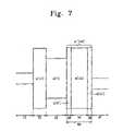
Referring to FIG. 7, a memory device according to additional embodiments of the present invention is shown. The memory device includes a semiconductor substrate 10, a tunneling insulating layer 20, a charge storage layer 22, a blocking insulating layer 64, and a gate electrode 27 disposed sequentially. The blocking insulating layer 64 includes a first silicon oxide layer 36 between a high dielectric layer 34 and a gate electrode 27 and a second silicon oxide layer 38 between the high dielectric layer 34 and the charge storage layer 22.
Equations 4 through 7 may describe the respective electric fields of the embodiments of the memory devices in FIGS. 4-7. For example, in the embodiments of FIGS. 5-7, a constant “∈(ob)” of the blocking insulating layers may be related to the constants of the dielectric layers and the oxide layer of the blocking insulating layers. When a blocking insulating layer of these embodiments has the same thickness as the blocking insulating layer of the memory device of FIG. 2, the electric field may become dependent upon the dielectric constant and the thickness of the dielectric layer. The oxide layer of the blocking insulating layer may increase a breakdown voltage of the blocking insulating layer. The oxide layer may also enhance an adhesiveness between the high dielectric layer and the gate electrode or between the high dielectric layer and the charge storage layer.
According to additional embodiments of the present invention, the dielectric layer 34 may comprise metallic oxide or metallic oxynitride of a group III element or group VB element in the Mendeleef Periodic Table. According to other embodiments, the dielectric layer 34 may comprise doped metal oxide or doped metal oxynitride in which metal oxide is doped with a group IV element in the Mendeleef Periodic Table. The group IV element may reduce leakage current from the memory device. The group IV element may be doped with a metal oxide of about 0.1-30 weight percent. The dielectric layer 34 may also comprise one of more of HfO2, Al2O3, La2O3, Hf1-xAlxOy, HfxSi1-xO2, Hf—Si-oxynitride, ZrO2, ZrxSi1-xO2, Zr—Si-oxynitride, and combinations thereof.
The material Al2O3 has a dielectric constant of 10 and an energy band gap of 8.3 eV and the material ZrO2 has a dielectric constant of 25 and an energy band gap of 8.3 eV. The dielectric layer 34 may also comprise one or more of AlO, Al2O3, Ta2O5, TiO2, PZT[Pb(Zr, Ti)O3], PbTiO3, PbZrO3, PZT[(Pb, La)(Zr, Ti)O3], PbO, SrTiO3, BaTiO3, V2O5, BST[(Ba, Sr)TiO3], SBT(SrBi2Ta2O9), Bi4Ti3O12, and combinations thereof.
The charge storage layer 22 may comprise one or more of Si3N4, silicon oxynitride, silicon-rich oxide, and other ferroelectric materials.
Referring to FIGS. 8-10, memory devices according to additional embodiments of the invention are shown. A plurality of active regions ACT are disposed on a semiconductor substrate 10. The active regions ACTs are parallel with one another along one direction of the substrate 10. A common source line CSL crosses over the active regions ACT. Bitline plugs DC are connected to the respective active regions ACT and separated from the common source line CSL by a predetermined distance. The bitline plugs DCs are parallel to the common source line CSL.
A string selection gate electrode 117 s and a ground selection gate electrode 117 g are parallel with each other, and cross over the active regions ACTs between the common source line CSL and the bitline plugs DCs. The string selection gate electrode 117 s is adjacent to the bitline plugs DCs, and the ground selection gate electrode 117 g is adjacent to the common source line CSL.
Between the string selection gate electrode 117 s and the ground selection gate electrode 117 g, a plurality of memory gate electrodes 117 m cross over the active regions ACTs. The memory gate electrodes 117 m are parallel with one another. A tunneling insulating layer 110, a charge storage layer 112, and a blocking insulating layer 114 are sequentially stacked between the active regions ACTs and the memory gate electrodes 117 m. The tunneling insulating layer 110, the charge storage layer 112, and the blocking insulating layer 114 can comprise the same materials as previously described.
An impurity-doped region 102 is on opposite sides of the string selection gate electrode 117 s, the ground selection gate electrode 117 g, and the memory gate electrodes 117 m. The common source line CSL is connected to the respective impurity-doped region (source region) 102 s that is adjacent to the ground selection electrode 117 g. An interlayer insulating film 120 covers the surface of a semiconductor substrate including the gate electrodes 117 g, 117 m, and 117 s and the common source line CSL. The bitline plugs DCs are connected to impurity-doped regions (drain regions) 102 d adjacent to the string selection gate 117 s. A plurality of bitlines BLs are formed on the interlayer insulating film 120 to cross over the gate electrodes 117 g, 117 m, and 117 s. The bitlines BLs are electrically connected to the bitline plug DC.
Memory cells may be provided at intersections of the respective memory gate electrodes 117 m and the active regions ACTs. Selection transistors may be provided at intersections of the respective selection gates 117 s and 117 g and the respective active regions ACTs.
As shown in FIG. 9, the memory device may include a tunnel insulating layer 110, a charge storage layer 112, and a blocking insulating layer 114 sequentially stacked to be between the ground selection gate electrode 117 g and the string selection gate electrode 117 s and the active regions (ACTs of FIG. 8). A negative voltage may be applied to the ground selection gate electrode 117 g and the string selection gate electrode 117 s to lower the threshold voltage of the selection transistor during memory operations.
According to further embodiments, as shown in FIG. 10, the memory device can include a gate insulating layer 116 between each of the ground selection gate electrode 117 g and the string selection gate electrode 117 s and the active regions (ACTs of FIG. 8). The gate insulating layer 116 can comprise silicon oxide, silicon oxynitride, or a combination thereof.
FIG. 11 is an energy band diagram of a nonvolatile memory device in accordance with a first embodiment of the invention.
Referring to FIG. 11, the nonvolatile memory device includes a semiconductor substrate 50, a tunnel insulation film 60, a charge-trapping layer 70, a blocking insulation film 110, and a gate electrode 100. The blocking insulation film 110 is formed as a stacked structure of a barrier insulation film 80 and a high-dielectric film 90. As illustrated, the high-dielectric film 90 has a potential barrier b1 relative to the charge-trapping film 70 and the barrier insulation film 80 has a potential barrier b2 relative to the charge-trapping film 70. The potential barrier b2 is greater than the potential barrier b1 of the high-dielectric film 90. For instance, an aluminum oxide film (which the high-dielectric film 90 may include) has a valence band with a barrier of 0.4 eV relative to a silicon nitride film, while a silicon oxide film (which the barrier insulating film 80 may include) has a valence band with a higher barrier of 1.1 eV relative to a silicon nitride film.
The thickness of the barrier insulation film 80 affects charge tunneling through the barrier insulation film 80 during a write-in (write) operation, and affects charge tunneling through the barrier insulating film 80 during an erase operation. Consequently, it may be important to control the thickness of the barrier insulation film 80 during fabrication to avoid or prevent a reduction in the rate at which writing and/or erasing operations can be carried out.
FIG. 12 is an energy band diagram during a write-in operation of a nonvolatile memory device in accordance with the first embodiment of the invention.
As illustrated FIG. 12, when the barrier insulation film 80 is relatively thinner (as indicated by solid lines), an energy level causes FN tunneling increases from the edge of the valence band of the charge-trapping layer by a level h2. Accordingly, even though electrons excited at the valence band of the charge-trapping layer move through the barrier insulation film 80 by means of an FN-tunneling, as indicated by the arrow Jb, electrons held in the charge-trapping layer are restrained from tunneling through the barrier insulation film 80, as indicated by the arrow Jb1.
In accordance with some embodiments of the invention, the barrier insulation film 80 functions to retain information in a data retention mode (i.e., retaining stored information in the memory device), and a thickness of the barrier insulating film 80 is controlled during fabrication to have a minimum thickness that reduces or minimizes a reduction in the rate at which writing and/or reading operations can be carried out in the associated memory device. In some embodiments, the thickness of the barrier insulation film is controlled to be in a range of about 5 Angstroms (Å) to about 15 Å.
FIG. 13 and FIG. 14 are energy band diagrams of a nonvolatile memory device in accordance with a second embodiment of the invention.
Referring to FIG. 13, in the nonvolatile memory device according to the second embodiment, a barrier insulation film 80 a is disposed between the high-dielectric film 90 and the gate electrode 100. In a retention mode, electrons, which are present in the valence band of the high-dielectric film 90 above the potential barrier of the high-dielectric film 90, can be restrained from moving toward the gate electrode 100 by a potential barrier of the barrier insulation film 80 a.
Referring to FIG. 14, during a write-in operation, a write-in voltage is applied between the semiconductor substrate 50 and the gate electrode 100. When the barrier insulation film 80 a is relatively thicker (as indicated by the broken lines), an energy level, at a location where the FN tunneling occurs in the barrier insulation film 80 a, is lower than the edge of the valence band of the high-dielectric film 90 by a level h3. Consequently, electrons at the valence band of the high-dielectric film 90 and electrons trapped in the high-dielectric film 90 can FN-tunnel through the barrier insulation film 80 a. In contrast, when the barrier insulation film 80 a is relatively thinner (as indicated by the solid lines), an energy level, at a location where the FN tunneling occurs in the barrier insulation film 80 a, is higher than the edge of the valence band of the high-dielectric film 90 by a level h4 and, thereby, restrains charge tunneling through the barrier insulation film 80 a.
FIG. 15 and FIG. 16 are energy band diagrams of a nonvolatile memory device in accordance with a third embodiment of the invention.
Referring to FIG. 15, in the nonvolatile memory device according to the third embodiment, a first barrier insulation film 80 b is between the charge-trapping layer 70 and the high-dielectric film 90, and a second barrier insulation film 80 c is between the high-dielectric film 90 and the gate electrode 100. In a retention mode, tunneling of electrons in the charge-trapping layer 70 is interrupted by a potential barrier of the first barrier insulation film 80 b, while tunneling of electrons in the valence band of the high-dielectric film 90 is interrupted by a potential barrier of the second barrier insulation film 80 c, and are thereby restrained from moving to the gate electrode 100.
Referring to FIG. 16, during a write-in operation, a write-in voltage is applied between the semiconductor substrate 50 and the gate electrode 100. When the first and second barrier insulation films 80 b and 80 c are relatively thicker, energy levels, at a location where the FN tunneling occurs in the first and second barrier insulation films 80 b and 80 c, are lower than the edges of the valence bands of the charge-trapping layer 70 and the high-dielectric film 90, respectively, by a predetermined level. In contrast, when the first and second barrier insulation films 80 b and 80 c are relatively thinner, energy levels, at a location where the FN tunneling occurs in the first and second barrier insulation films 80 b and 80 c, are higher than the edges of the valence bands of the charge-trapping layer 70 and the high-dielectric film 90, respectively, by a predetermined level and thereby restrains charge tunneling through the first and second barrier insulation films 80 b and 80 c.
FIG. 17 is a flow chart showing methods of fabricating a nonvolatile memory device in accordance with various embodiments of the invention.
Referring to FIG. 17, the tunnel insulation film 60 is formed on the semiconductor substrate 50 (step S1). The tunnel insulation film 60 may, for example, be formed of a silicon oxide film or a multi-level insulation film including a silicon oxide film. The charge-trapping layer 70 is then formed on the tunnel insulation film 60 (step S2). The charge-trapping layer 70 may be formed of an insulation film including a high density of trap sites and/or an insulation film embedding conductive nano-particles. For example, the charge-trapping layer 70 may be formed of a silicon nitride film or a silicon nitride film having nano-particles therein.
The top of the charge-trapping layer 70 is then oxidized so as to be transformed into the barrier insulation film 80 a (step S3). The barrier insulation film 80 a can be formed from silicon oxide by oxidizing the top of the charge-trapping layer 70 with oxygen plasma and/or radicals including oxygen. For example, when the charge-trapping layer (70) is formed of silicon nitride, a silicon oxide film can be formed by plasma-treating the top of the silicon nitride film and/or radical-processing the top of the silicon nitride film with oxygen or hydroxyl radicals. By forming the silicon oxide film with such plasma and/or radicals, the barrier insulation film 80 a may be formed having a thickness of between about 5 Å and about 15 Å.
Alternatively, the barrier insulation film 80 a may be formed by an atomic layer deposition (ALD) process. When using an ALD process, the quality of silicon oxide film used for the barrier insulation film 80 a may become more important to control. The silicon oxide film formed by way of plasma or radical treatment may have a high interface characteristic relative to the silicon nitride film in the charge-trapping layer 70, and may reliably form the barrier insulation film 80 a. The ALD process may be carried out directly on the charge trapping layer to more reliably form the barrier insulation film.
As a modification of the embodiments shown in FIG. 10, the barrier insulation film 80 a may be formed on the high-dielectric film 90. Also in these modified embodiments, the barrier insulation film 80 a may be formed by oxidizing the top of the high-dielectric film 90 with plasma or radicals. By oxidizing the top of the high-dielectric film, as shown in FIG. 13, a nonvolatile memory device may be fabricated with a thin barrier insulation film having a thickness in a range of about 5 Å to about 15 Å.
In some other embodiments of the invention, the fabrication steps for oxidizing the top of the charge-trapping layer 70 may be carried out after depositing the charge-trapping layer 70. The fabrication steps for oxidizing the top of the high-dielectric film 90 may be carried out after depositing the high-dielectric film 90. Accordingly, as illustrated in FIG. 8, the first barrier insulation film 80 b may be formed between the charge-trapping layer 70 and the high-dielectric film 90, and the second barrier insulation film 80 c may be formed between the high-dielectric film 90 and the gate electrode film 100.
By using the high-dielectric film as the blocking insulation film, an electric field generated at the blocking insulation film during write-in operations and erasing operations may be reduced, which may enhance the rate at which writing and/or erasing operations may be carried out.
Further, by forming the blocking insulation film from a stacked film structure of the high-dielectric film and the barrier insulation film, and where the high-dielectric film has a first potential barrier relative to the charge-trapping layer and the barrier insulation film has a second potential barrier relative to the charge-trapping layer which is higher than the first potential barrier, it may be possible to substantially inhibit/prevent charges from vanishing into the barrier insulation film of the charge-trapping layer during a retention mode.
By minimizing a thickness of the barrier insulation film, the valence band of the high-dielectric film may be less affected, and FN tunneling through the barrier insulation film may be less inhibited during a write-in operation. Thus, write-in and erasing operations may be carried out at a relatively high rate compared to a case where the blocking insulation film is formed of a single layer with a high-dielectric material.
The above-disclosed subject matter is to be considered illustrative, and not restrictive, and the appended claims are intended to cover all such modifications, enhancements, and other embodiments, which fall within the spirit and scope of the present invention. Thus, the scope of the present invention is to be determined by the broadest permissible interpretation of the following claims and their equivalents, and shall not be restricted or limited by the foregoing detailed description.

Claims (10)

1. A nonvolatile memory device comprising:
a tunnel insulation film on a semiconductor substrate;
a charge-trapping layer on the tunnel insulation film;
a blocking insulation film on the charge-trapping layer; and
a gate electrode formed on the blocking insulation film,
wherein the blocking insulation film comprises a stacked film structure of a high-dielectric film and a barrier insulation film, the high-dielectric film has a first potential barrier relative to the charge-trapping layer, the barrier insulation film has a second potential barrier relative to the charge-trapping layer which is higher than the first potential barrier, and the blocking insulation film has a thickness in a range of about 5 Å to about 15 Å.
2. The nonvolatile memory device as set forth in claim 1, wherein the barrier insulation film comprises the silicon oxide film.
3. The nonvolatile memory device as set forth in claim 2, wherein:
the charge-trapping layer comprises a silicon nitride film; and
the barrier insulation film comprises the silicon oxide film as an oxidation layer on a surface of the silicon nitride film.
4. A method of fabricating a nonvolatile memory device, the method comprising:
forming a tunnel insulation film on a semiconductor substrate;
forming a charge-trapping layer on the tunnel insulation film;
forming a blocking insulation film on the charge-trapping layer as a stacked film structure, wherein the blocking insulating film is formed from a stacked film structure of high-dielectric film and a barrier insulation film, wherein the high-dielectric film has a first potential barrier relative to the charge-trapping layer, the barrier insulation film has a second potential barrier relative to the charge-trapping layer which is higher than the first potential barrier, and the barrier insulation film is formed to have a thickness in a range of about 5 Å to about 15 Å.
5. The method as set forth in claim 4, wherein the barrier insulation film is formed as the silicon oxide film.
6. The method as set forth in claim 4, wherein forming the blocking insulation film comprises oxidizing a surface of the charge-trapping layer to form the barrier insulation film.
7. The method as set forth in claim 6, wherein oxidizing a surface of the charge-trapping layer to form the barrier insulation film comprises applying an oxygen plasma to oxidize an upper surface of the charge-trapping layer.
8. The method as set forth in claim 6, wherein oxidizing a surface of the charge-trapping layer to form the barrier insulation film comprises applying radicals containing oxygen to oxidize an upper surface of the charge-trapping layer.
9. The method as set forth in claim 6, wherein:
forming a charge-trapping layer comprises forming a silicon nitride film as the charge-trapping layer; and
the barrier insulation film is formed as the silicon oxide film by oxidizing a surface of the silicon nitride film.
10. The method as set forth in claim 4, wherein the barrier insulation film is formed by an atomic layer deposition (ALD) process on the charge trapping layer.
US11/601,505 2001-06-28 2006-11-17 Non-volatile semiconductor memory devices and methods of fabricating the same Active 2025-09-10 US7473959B2 (en)

Priority Applications (1)

Application Number Priority Date Filing Date Title
US11/601,505 US7473959B2 (en) 2001-06-28 2006-11-17 Non-volatile semiconductor memory devices and methods of fabricating the same

Applications Claiming Priority (8)

Application Number Priority Date Filing Date Title
KR2001-0037421 2001-06-28
KR20010037421 2001-06-28
KR2002-0005622 2002-01-31
KR10-2002-0005622A KR100456580B1 (en) 2001-06-28 2002-01-31 Floating trap type memory device of non-volatile semiconductor memory device
US11/043,485 US7400009B2 (en) 2001-06-28 2005-01-26 Floating trap non-volatile semiconductor memory devices including high dielectric constant blocking insulating layers
KR1020060047231A KR100794655B1 (en) 2006-05-25 2006-05-25 Non-volatile memory device and method of fabricating the same
KR10-2006-0047231 2006-05-25
US11/601,505 US7473959B2 (en) 2001-06-28 2006-11-17 Non-volatile semiconductor memory devices and methods of fabricating the same

Related Parent Applications (1)

Application Number Title Priority Date Filing Date
US11/043,485 Continuation-In-Part US7400009B2 (en) 2001-06-28 2005-01-26 Floating trap non-volatile semiconductor memory devices including high dielectric constant blocking insulating layers

Publications (2)

Publication Number Publication Date
US20070063265A1 US20070063265A1 (en) 2007-03-22
US7473959B2 true US7473959B2 (en) 2009-01-06

Family

ID=37883212

Family Applications (1)

Application Number Title Priority Date Filing Date
US11/601,505 Active 2025-09-10 US7473959B2 (en) 2001-06-28 2006-11-17 Non-volatile semiconductor memory devices and methods of fabricating the same

Country Status (1)

Country Link
US (1) US7473959B2 (en)

Cited By (2)

* Cited by examiner, † Cited by third party
Publication number Priority date Publication date Assignee Title
US20090032910A1 (en) * 2004-12-13 2009-02-05 Micron Technology, Inc. Dielectric stack containing lanthanum and hafnium
US20090159962A1 (en) * 2007-12-20 2009-06-25 Samsung Electronics Co., Ltd. Non-Volatile Memory Devices

Families Citing this family (2)

* Cited by examiner, † Cited by third party
Publication number Priority date Publication date Assignee Title
JP5295606B2 (en) 2008-03-28 2013-09-18 株式会社東芝 NAND type nonvolatile semiconductor memory device
KR101512494B1 (en) * 2009-01-09 2015-04-16 삼성전자주식회사 Method of fabricating semiconductor device

Citations (60)

* Cited by examiner, † Cited by third party
Publication number Priority date Publication date Assignee Title
US4630086A (en) 1982-09-24 1986-12-16 Hitachi, Ltd. Nonvolatile MNOS memory
JPS63141A (en) 1986-06-19 1988-01-05 Fujitsu Ltd Semiconductor memory
US4870470A (en) 1987-10-16 1989-09-26 International Business Machines Corporation Non-volatile memory cell having Si rich silicon nitride charge trapping layer
US5270298A (en) 1992-03-05 1993-12-14 Bell Communications Research, Inc. Cubic metal oxide thin film epitaxially grown on silicon
US5424567A (en) 1991-05-15 1995-06-13 North American Philips Corporation Protected programmable transistor with reduced parasitic capacitances and method of fabrication
JPH0817945A (en) 1994-06-27 1996-01-19 Nec Corp Semiconductor storage device and its manufacture
JPH08162549A (en) 1994-05-25 1996-06-21 Hyundai Electron Ind Co Ltd Formation method of gate electrode of semiconductor element
US5583067A (en) 1993-01-22 1996-12-10 Intel Corporation Inverse T-gate semiconductor device with self-aligned punchthrough stops and method of fabrication
JPH09129757A (en) 1995-10-27 1997-05-16 Nkk Corp Non-volatile semiconductor memory device and manufacture thereof
US5768192A (en) 1996-07-23 1998-06-16 Saifun Semiconductors, Ltd. Non-volatile semiconductor memory cell utilizing asymmetrical charge trapping
JPH118325A (en) 1997-04-25 1999-01-12 Nippon Steel Corp Nonvolatile semiconductor device, its manufacturing method, its writing method, its reading method, storage medium and semiconductor device
US5923056A (en) 1996-10-10 1999-07-13 Lucent Technologies Inc. Electronic components with doped metal oxide dielectric materials and a process for making electronic components with doped metal oxide dielectric materials
US6011725A (en) 1997-08-01 2000-01-04 Saifun Semiconductors, Ltd. Two bit non-volatile electrically erasable and programmable semiconductor memory cell utilizing asymmetrical charge trapping
US6141256A (en) 1997-01-29 2000-10-31 Micron Technology, Inc. Differential flash memory cell and method for programming same
WO2000075997A1 (en) 1999-06-08 2000-12-14 Infineon Technologies Ag Non-volatile semiconductor memory cell, comprising a metal-oxide dielectric and a method for producing the same
US6163049A (en) 1998-10-13 2000-12-19 Advanced Micro Devices, Inc. Method of forming a composite interpoly gate dielectric
US6166958A (en) * 1998-07-09 2000-12-26 Kabushiki Kaisha Toshiba Semiconductor memory device, method for manufacturing the same, and method for controlling the same
JP2001035945A (en) 1999-06-28 2001-02-09 Hyundai Electronics Ind Co Ltd Method for forming gate of stack flash type flash eeprom cell
US6225646B1 (en) 2000-01-14 2001-05-01 Advanced Micro Devices, Inc. Integrated circuit incorporating a memory cell and a transistor elevated above an insulating base
US6236076B1 (en) 1999-04-29 2001-05-22 Symetrix Corporation Ferroelectric field effect transistors for nonvolatile memory applications having functional gradient material
KR20010066386A (en) 1999-12-31 2001-07-11 박종섭 Method of forming gate electrode of Flash memory
US6287915B1 (en) 1997-11-19 2001-09-11 Nec Corporation Semiconductor device and manufacturing method therefor
US6294436B1 (en) 1999-08-16 2001-09-25 Infineon Technologies Ag Method for fabrication of enlarged stacked capacitors using isotropic etching
US6297517B1 (en) 2000-02-28 2001-10-02 Matsushita Electric Industrial Co., Ltd. Semiconductor device and method of fabricating the same
WO2001077319A2 (en) 2000-04-07 2001-10-18 Microbiological Research Authority Genetic manipulation of clostridium difficile
US6307775B1 (en) 1997-07-29 2001-10-23 Micron Technology, Inc. Deaprom and transistor with gallium nitride or gallium aluminum nitride gate
US6417537B1 (en) 2000-01-18 2002-07-09 Micron Technology, Inc. Metal oxynitride capacitor barrier layer
JP2002203917A (en) 2000-10-26 2002-07-19 Sony Corp Nonvolatile semiconductor storage device and its manufacturing method
US6458677B1 (en) 1999-10-25 2002-10-01 Advanced Micro Devices, Inc. Process for fabricating an ONO structure
US6465828B2 (en) 1999-07-30 2002-10-15 Micron Technology, Inc. Semiconductor container structure with diffusion barrier
US6489649B2 (en) 1996-12-26 2002-12-03 Hitachi, Ltd. Semiconductor device having nonvolatile memory and method of manufacturing thereof
US6512274B1 (en) 2000-06-22 2003-01-28 Progressant Technologies, Inc. CMOS-process compatible, tunable NDR (negative differential resistance) device and method of operating same
KR20030057851A (en) 2001-12-29 2003-07-07 주식회사 하이닉스반도체 metal line of Nonvolatile Ferroelectric memory
US20030155605A1 (en) 2002-02-15 2003-08-21 Macronix International Co., Ltd. EEPROM memory cell with high radiation resistance
US6614069B2 (en) 1999-07-20 2003-09-02 Infineon Technologies Ag Nonvolatile semiconductor memory cell and method for fabricating the memory cell
US20030183873A1 (en) 1998-11-04 2003-10-02 Ichiro Fujiwara Nonvolatile semiconductor memory device and process of production and write method thereof
JP2003332467A (en) 2000-09-05 2003-11-21 Seiko Epson Corp Semiconductor device
US20040021170A1 (en) 1999-03-24 2004-02-05 Caywood John M. Method and apparatus for injecting charge onto the floating gate of a nonvolatile memory cell
US6706599B1 (en) 2003-03-20 2004-03-16 Motorola, Inc. Multi-bit non-volatile memory device and method therefor
US6730960B2 (en) 2000-02-29 2004-05-04 Micron Technology, Inc. Static NVRAM with ultra thin tunnel oxides
KR20040054146A (en) 2002-12-17 2004-06-25 주식회사 하이닉스반도체 Method for forming a tunnel oxide and method for forming floating gate in flash memory device using the same
US6791883B2 (en) 2002-06-24 2004-09-14 Freescale Semiconductor, Inc. Program and erase in a thin film storage non-volatile memory
US6803272B1 (en) 2001-12-31 2004-10-12 Advanced Micro Devices, Inc. Use of high-K dielectric material in modified ONO structure for semiconductor devices
KR20040106074A (en) 2003-06-10 2004-12-17 삼성전자주식회사 SONOS memory device and method of manufacturing the same
KR20040108309A (en) 2003-06-10 2004-12-23 삼성전자주식회사 SONOS memory device and method of manufacturing the same
US6844604B2 (en) 2001-02-02 2005-01-18 Samsung Electronics Co., Ltd. Dielectric layer for semiconductor device and method of manufacturing the same
US20050023603A1 (en) 2001-08-30 2005-02-03 Micron Technology, Inc. Atomic layer deposition of metal oxide and/or low asymmetrical tunnel barrier interpoly insulators
US6858899B2 (en) 2002-10-15 2005-02-22 Matrix Semiconductor, Inc. Thin film transistor with metal oxide layer and method of making same
US6885058B2 (en) 2000-03-08 2005-04-26 Koninklijke Philips Electronics N.V. Semiconductor device and method of manufacturing such a semiconductor device
US6906366B2 (en) 2001-03-28 2005-06-14 Sharp Laboratories Of America, Inc. Single transistor ferroelectric transistor structure with high-k insulator
US6924186B2 (en) 2000-03-21 2005-08-02 Micron Technology, Inc. Method of forming a memory device and semiconductor device
US20050189600A1 (en) 1998-10-08 2005-09-01 Kabushiki Kaisha Toshiba Semiconductor device having gate electrode of staked structure including polysilicon layer and metal layer and method of manufacturing the same
US6949788B2 (en) 1999-12-17 2005-09-27 Sony Corporation Nonvolatile semiconductor memory device and method for operating the same
KR20050102864A (en) 2004-04-23 2005-10-27 삼성전자주식회사 Memory device with dielectric multilayer and method of manufacturing the same
US6963103B2 (en) 2001-08-30 2005-11-08 Micron Technology, Inc. SRAM cells with repressed floating gate memory, low tunnel barrier interpoly insulators
US20060022252A1 (en) 2004-07-30 2006-02-02 Samsung Electronics Co., Ltd. Nonvolatile memory device and method of fabricating the same
US7087954B2 (en) 2001-08-30 2006-08-08 Micron Technology, Inc. In service programmable logic arrays with low tunnel barrier interpoly insulators
JP2006229195A (en) 2005-01-24 2006-08-31 Renesas Technology Corp Semiconductor nonvolatile memory and its manufacturing method
US7109548B2 (en) 1997-07-29 2006-09-19 Micron Technology, Inc. Operating a memory device
US20060270157A1 (en) 2005-05-30 2006-11-30 Hynix Semiconductor Inc. Method of manufacturing flash memory device

Family Cites Families (1)

* Cited by examiner, † Cited by third party
Publication number Priority date Publication date Assignee Title
US6238076B1 (en) * 1999-03-29 2001-05-29 Primetech Electronics, Inc. Compact light mixing and diffusing apparatus

Patent Citations (70)

* Cited by examiner, † Cited by third party
Publication number Priority date Publication date Assignee Title
US4630086A (en) 1982-09-24 1986-12-16 Hitachi, Ltd. Nonvolatile MNOS memory
JPS63141A (en) 1986-06-19 1988-01-05 Fujitsu Ltd Semiconductor memory
US4870470A (en) 1987-10-16 1989-09-26 International Business Machines Corporation Non-volatile memory cell having Si rich silicon nitride charge trapping layer
US5424567A (en) 1991-05-15 1995-06-13 North American Philips Corporation Protected programmable transistor with reduced parasitic capacitances and method of fabrication
US5270298A (en) 1992-03-05 1993-12-14 Bell Communications Research, Inc. Cubic metal oxide thin film epitaxially grown on silicon
US5583067A (en) 1993-01-22 1996-12-10 Intel Corporation Inverse T-gate semiconductor device with self-aligned punchthrough stops and method of fabrication
JPH08162549A (en) 1994-05-25 1996-06-21 Hyundai Electron Ind Co Ltd Formation method of gate electrode of semiconductor element
US5536667A (en) 1994-05-25 1996-07-16 Hyundai Electronics Industries Co., Ltd. Method for forming a gate electrode in a semiconductor device
US5619051A (en) 1994-06-27 1997-04-08 Nec Corporation Semiconductor nonvolatile memory cell
JPH0817945A (en) 1994-06-27 1996-01-19 Nec Corp Semiconductor storage device and its manufacture
JPH09129757A (en) 1995-10-27 1997-05-16 Nkk Corp Non-volatile semiconductor memory device and manufacture thereof
US5768192A (en) 1996-07-23 1998-06-16 Saifun Semiconductors, Ltd. Non-volatile semiconductor memory cell utilizing asymmetrical charge trapping
US5923056A (en) 1996-10-10 1999-07-13 Lucent Technologies Inc. Electronic components with doped metal oxide dielectric materials and a process for making electronic components with doped metal oxide dielectric materials
US6489649B2 (en) 1996-12-26 2002-12-03 Hitachi, Ltd. Semiconductor device having nonvolatile memory and method of manufacturing thereof
US6141256A (en) 1997-01-29 2000-10-31 Micron Technology, Inc. Differential flash memory cell and method for programming same
JPH118325A (en) 1997-04-25 1999-01-12 Nippon Steel Corp Nonvolatile semiconductor device, its manufacturing method, its writing method, its reading method, storage medium and semiconductor device
US7109548B2 (en) 1997-07-29 2006-09-19 Micron Technology, Inc. Operating a memory device
US6307775B1 (en) 1997-07-29 2001-10-23 Micron Technology, Inc. Deaprom and transistor with gallium nitride or gallium aluminum nitride gate
US7116577B2 (en) 1997-08-01 2006-10-03 Saifun Semiconductors Ltd Two bit non-volatile electrically erasable and programmable semiconductor memory cell utilizing asymmetrical charge trapping
US6011725A (en) 1997-08-01 2000-01-04 Saifun Semiconductors, Ltd. Two bit non-volatile electrically erasable and programmable semiconductor memory cell utilizing asymmetrical charge trapping
US6768165B1 (en) 1997-08-01 2004-07-27 Saifun Semiconductors Ltd. Two bit non-volatile electrically erasable and programmable semiconductor memory cell utilizing asymmetrical charge trapping
US6287915B1 (en) 1997-11-19 2001-09-11 Nec Corporation Semiconductor device and manufacturing method therefor
US6166958A (en) * 1998-07-09 2000-12-26 Kabushiki Kaisha Toshiba Semiconductor memory device, method for manufacturing the same, and method for controlling the same
US20050189600A1 (en) 1998-10-08 2005-09-01 Kabushiki Kaisha Toshiba Semiconductor device having gate electrode of staked structure including polysilicon layer and metal layer and method of manufacturing the same
US6163049A (en) 1998-10-13 2000-12-19 Advanced Micro Devices, Inc. Method of forming a composite interpoly gate dielectric
US20030183873A1 (en) 1998-11-04 2003-10-02 Ichiro Fujiwara Nonvolatile semiconductor memory device and process of production and write method thereof
US20040021170A1 (en) 1999-03-24 2004-02-05 Caywood John M. Method and apparatus for injecting charge onto the floating gate of a nonvolatile memory cell
US6236076B1 (en) 1999-04-29 2001-05-22 Symetrix Corporation Ferroelectric field effect transistors for nonvolatile memory applications having functional gradient material
WO2000075997A1 (en) 1999-06-08 2000-12-14 Infineon Technologies Ag Non-volatile semiconductor memory cell, comprising a metal-oxide dielectric and a method for producing the same
US6204125B1 (en) 1999-06-28 2001-03-20 Hyundai Electronics Industries Co., Ltd. Method of forming a gate in a stack gate flash EEPROM cell
JP2001035945A (en) 1999-06-28 2001-02-09 Hyundai Electronics Ind Co Ltd Method for forming gate of stack flash type flash eeprom cell
US6614069B2 (en) 1999-07-20 2003-09-02 Infineon Technologies Ag Nonvolatile semiconductor memory cell and method for fabricating the memory cell
US6465828B2 (en) 1999-07-30 2002-10-15 Micron Technology, Inc. Semiconductor container structure with diffusion barrier
US6294436B1 (en) 1999-08-16 2001-09-25 Infineon Technologies Ag Method for fabrication of enlarged stacked capacitors using isotropic etching
US6458677B1 (en) 1999-10-25 2002-10-01 Advanced Micro Devices, Inc. Process for fabricating an ONO structure
US6949788B2 (en) 1999-12-17 2005-09-27 Sony Corporation Nonvolatile semiconductor memory device and method for operating the same
US6627494B2 (en) 1999-12-31 2003-09-30 Hynix Semiconductor Inc. Method for forming gate electrode of flash memory
KR20010066386A (en) 1999-12-31 2001-07-11 박종섭 Method of forming gate electrode of Flash memory
US6225646B1 (en) 2000-01-14 2001-05-01 Advanced Micro Devices, Inc. Integrated circuit incorporating a memory cell and a transistor elevated above an insulating base
US6417537B1 (en) 2000-01-18 2002-07-09 Micron Technology, Inc. Metal oxynitride capacitor barrier layer
US6297517B1 (en) 2000-02-28 2001-10-02 Matsushita Electric Industrial Co., Ltd. Semiconductor device and method of fabricating the same
US6730960B2 (en) 2000-02-29 2004-05-04 Micron Technology, Inc. Static NVRAM with ultra thin tunnel oxides
US6885058B2 (en) 2000-03-08 2005-04-26 Koninklijke Philips Electronics N.V. Semiconductor device and method of manufacturing such a semiconductor device
US6924186B2 (en) 2000-03-21 2005-08-02 Micron Technology, Inc. Method of forming a memory device and semiconductor device
WO2001077319A2 (en) 2000-04-07 2001-10-18 Microbiological Research Authority Genetic manipulation of clostridium difficile
US6512274B1 (en) 2000-06-22 2003-01-28 Progressant Technologies, Inc. CMOS-process compatible, tunable NDR (negative differential resistance) device and method of operating same
JP2003332467A (en) 2000-09-05 2003-11-21 Seiko Epson Corp Semiconductor device
JP2002203917A (en) 2000-10-26 2002-07-19 Sony Corp Nonvolatile semiconductor storage device and its manufacturing method
US6844604B2 (en) 2001-02-02 2005-01-18 Samsung Electronics Co., Ltd. Dielectric layer for semiconductor device and method of manufacturing the same
US6906366B2 (en) 2001-03-28 2005-06-14 Sharp Laboratories Of America, Inc. Single transistor ferroelectric transistor structure with high-k insulator
US20050023603A1 (en) 2001-08-30 2005-02-03 Micron Technology, Inc. Atomic layer deposition of metal oxide and/or low asymmetrical tunnel barrier interpoly insulators
US7087954B2 (en) 2001-08-30 2006-08-08 Micron Technology, Inc. In service programmable logic arrays with low tunnel barrier interpoly insulators
US6963103B2 (en) 2001-08-30 2005-11-08 Micron Technology, Inc. SRAM cells with repressed floating gate memory, low tunnel barrier interpoly insulators
KR20030057851A (en) 2001-12-29 2003-07-07 주식회사 하이닉스반도체 metal line of Nonvolatile Ferroelectric memory
US6803272B1 (en) 2001-12-31 2004-10-12 Advanced Micro Devices, Inc. Use of high-K dielectric material in modified ONO structure for semiconductor devices
US20030155605A1 (en) 2002-02-15 2003-08-21 Macronix International Co., Ltd. EEPROM memory cell with high radiation resistance
US6791883B2 (en) 2002-06-24 2004-09-14 Freescale Semiconductor, Inc. Program and erase in a thin film storage non-volatile memory
US6858899B2 (en) 2002-10-15 2005-02-22 Matrix Semiconductor, Inc. Thin film transistor with metal oxide layer and method of making same
KR20040054146A (en) 2002-12-17 2004-06-25 주식회사 하이닉스반도체 Method for forming a tunnel oxide and method for forming floating gate in flash memory device using the same
US6706599B1 (en) 2003-03-20 2004-03-16 Motorola, Inc. Multi-bit non-volatile memory device and method therefor
KR20040108309A (en) 2003-06-10 2004-12-23 삼성전자주식회사 SONOS memory device and method of manufacturing the same
KR20040106074A (en) 2003-06-10 2004-12-17 삼성전자주식회사 SONOS memory device and method of manufacturing the same
KR20050102864A (en) 2004-04-23 2005-10-27 삼성전자주식회사 Memory device with dielectric multilayer and method of manufacturing the same
US20050247970A1 (en) 2004-04-23 2005-11-10 Samsung Electronics Co., Ltd., Memory device including a dielectric multilayer structure and method of fabricating the same
KR20060011478A (en) 2004-07-30 2006-02-03 삼성전자주식회사 Non volatile memory device and method for manufacturing thereof
US20060022252A1 (en) 2004-07-30 2006-02-02 Samsung Electronics Co., Ltd. Nonvolatile memory device and method of fabricating the same
JP2006229195A (en) 2005-01-24 2006-08-31 Renesas Technology Corp Semiconductor nonvolatile memory and its manufacturing method
US20060270157A1 (en) 2005-05-30 2006-11-30 Hynix Semiconductor Inc. Method of manufacturing flash memory device
KR20060124001A (en) 2005-05-30 2006-12-05 주식회사 하이닉스반도체 Method of manufacturing a flash memory device
JP2006339624A (en) 2005-05-30 2006-12-14 Hynix Semiconductor Inc Method of manufacturing flash memory device

Cited By (5)

* Cited by examiner, † Cited by third party
Publication number Priority date Publication date Assignee Title
US20090032910A1 (en) * 2004-12-13 2009-02-05 Micron Technology, Inc. Dielectric stack containing lanthanum and hafnium
US20090159962A1 (en) * 2007-12-20 2009-06-25 Samsung Electronics Co., Ltd. Non-Volatile Memory Devices
US7973357B2 (en) * 2007-12-20 2011-07-05 Samsung Electronics Co., Ltd. Non-volatile memory devices
US20110198685A1 (en) * 2007-12-20 2011-08-18 Hyun-Suk Kim Non-Volatile Memory Devices
US8314457B2 (en) 2007-12-20 2012-11-20 Samsung Electronics Co., Ltd. Non-volatile memory devices

Also Published As

Publication number Publication date
US20070063265A1 (en) 2007-03-22

Similar Documents

Publication Publication Date Title
US7400009B2 (en) Floating trap non-volatile semiconductor memory devices including high dielectric constant blocking insulating layers
US7253467B2 (en) Non-volatile semiconductor memory devices
US9761314B2 (en) Non-volatile memory devices and methods of operating the same
US7420256B2 (en) Nonvolatile semiconductor memory device having a gate stack and method of manufacturing the same
JP5160470B2 (en) Floating trap type non-volatile memory device
US7576386B2 (en) Non-volatile memory semiconductor device having an oxide-nitride-oxide (ONO) top dielectric layer
US20080093661A1 (en) Non-volatile memory device having a charge trapping layer and method for fabricating the same
US20050093054A1 (en) Non-volatile memory devices and methods of fabricating the same
US8044454B2 (en) Non-volatile memory device
US20050167734A1 (en) Flash memory devices using large electron affinity material for charge trapping
US8975687B2 (en) Nonvolatile memory array with continuous charge storage dielectric stack
US7473959B2 (en) Non-volatile semiconductor memory devices and methods of fabricating the same
KR100684900B1 (en) Non-volatile memory device and method of operating the same
US7855114B2 (en) High K stack for non-volatile memory
KR100688586B1 (en) Sonos nonvolatile memory device having local charge trap layer and driving method thereof
KR101244842B1 (en) Operating method of charge trap flash memory device
KR101149572B1 (en) Nonvolatile memory device with staggered tunnel barrier

Legal Events

Date Code Title Description
AS Assignment

Owner name: SAMSUNG ELECTRONICS CO., LTD., KOREA, REPUBLIC OF

Free format text: ASSIGNMENT OF ASSIGNORS INTEREST;ASSIGNORS:LEE, SUNG-HAE;LEE, CHUNG-HYUN;HWANG, KI-HYUN;AND OTHERS;REEL/FRAME:018617/0173

Effective date: 20061102

AS Assignment

Owner name: SAMSUNG ELECTRONICS CO., LTD., KOREA, REPUBLIC OF

Free format text: RE-RECORD TO CORRECT THE NAME OF THE SECOND ASSIGNOR, PREVIOUSLY RECORDED ON REEL 018617 FRAME 0173.;ASSIGNORS:LEE, SUNG-HAE;LEE, CHANG-HYUN;HWANG, KI-HYUN;AND OTHERS;REEL/FRAME:018764/0332

Effective date: 20061102

STCF Information on status: patent grant

Free format text: PATENTED CASE

FPAY Fee payment

Year of fee payment: 4

FPAY Fee payment

Year of fee payment: 8

MAFP Maintenance fee payment

Free format text: PAYMENT OF MAINTENANCE FEE, 12TH YEAR, LARGE ENTITY (ORIGINAL EVENT CODE: M1553); ENTITY STATUS OF PATENT OWNER: LARGE ENTITY

Year of fee payment: 12