US7459400B2 - Patterned structures fabricated by printing mask over lift-off pattern - Google Patents
Patterned structures fabricated by printing mask over lift-off pattern Download PDFInfo
- Publication number
- US7459400B2 US7459400B2 US11/184,304 US18430405A US7459400B2 US 7459400 B2 US7459400 B2 US 7459400B2 US 18430405 A US18430405 A US 18430405A US 7459400 B2 US7459400 B2 US 7459400B2
- Authority
- US
- United States
- Prior art keywords
- pattern
- lift
- portions
- mask
- layer
- Prior art date
- Legal status (The legal status is an assumption and is not a legal conclusion. Google has not performed a legal analysis and makes no representation as to the accuracy of the status listed.)
- Active, expires
Links
- 238000007639 printing Methods 0.000 title claims abstract description 74
- 238000000034 method Methods 0.000 claims abstract description 107
- 239000000758 substrate Substances 0.000 claims abstract description 32
- 239000010409 thin film Substances 0.000 claims abstract description 7
- 229910052751 metal Inorganic materials 0.000 claims description 43
- 239000002184 metal Substances 0.000 claims description 43
- 239000012530 fluid Substances 0.000 claims description 12
- 238000000059 patterning Methods 0.000 claims description 11
- 238000000151 deposition Methods 0.000 claims description 10
- 239000012782 phase change material Substances 0.000 claims description 9
- 230000002093 peripheral effect Effects 0.000 claims description 7
- 239000002904 solvent Substances 0.000 claims description 7
- 239000011800 void material Substances 0.000 claims description 7
- 230000009471 action Effects 0.000 claims description 6
- 238000005530 etching Methods 0.000 claims description 6
- 238000009736 wetting Methods 0.000 claims description 4
- 238000010438 heat treatment Methods 0.000 claims description 3
- 238000000527 sonication Methods 0.000 claims description 3
- 230000008569 process Effects 0.000 abstract description 51
- 229920002120 photoresistant polymer Polymers 0.000 abstract description 24
- 238000001039 wet etching Methods 0.000 abstract description 8
- 239000010410 layer Substances 0.000 description 163
- 238000004519 manufacturing process Methods 0.000 description 29
- 229910021417 amorphous silicon Inorganic materials 0.000 description 12
- 239000004065 semiconductor Substances 0.000 description 11
- 230000015572 biosynthetic process Effects 0.000 description 8
- 239000000463 material Substances 0.000 description 8
- 238000000206 photolithography Methods 0.000 description 8
- VYZAMTAEIAYCRO-UHFFFAOYSA-N Chromium Chemical compound [Cr] VYZAMTAEIAYCRO-UHFFFAOYSA-N 0.000 description 5
- 229910052804 chromium Inorganic materials 0.000 description 5
- 239000011651 chromium Substances 0.000 description 5
- 238000001000 micrograph Methods 0.000 description 5
- VYPSYNLAJGMNEJ-UHFFFAOYSA-N Silicium dioxide Chemical compound O=[Si]=O VYPSYNLAJGMNEJ-UHFFFAOYSA-N 0.000 description 4
- 230000008021 deposition Effects 0.000 description 4
- YXFVVABEGXRONW-UHFFFAOYSA-N Toluene Chemical compound CC1=CC=CC=C1 YXFVVABEGXRONW-UHFFFAOYSA-N 0.000 description 3
- 239000012776 electronic material Substances 0.000 description 3
- 238000004381 surface treatment Methods 0.000 description 3
- 239000000725 suspension Substances 0.000 description 3
- 229910052581 Si3N4 Inorganic materials 0.000 description 2
- WYURNTSHIVDZCO-UHFFFAOYSA-N Tetrahydrofuran Chemical compound C1CCOC1 WYURNTSHIVDZCO-UHFFFAOYSA-N 0.000 description 2
- 229910052782 aluminium Inorganic materials 0.000 description 2
- XAGFODPZIPBFFR-UHFFFAOYSA-N aluminium Chemical compound [Al] XAGFODPZIPBFFR-UHFFFAOYSA-N 0.000 description 2
- 238000003491 array Methods 0.000 description 2
- QVGXLLKOCUKJST-UHFFFAOYSA-N atomic oxygen Chemical compound [O] QVGXLLKOCUKJST-UHFFFAOYSA-N 0.000 description 2
- 230000009286 beneficial effect Effects 0.000 description 2
- 230000008901 benefit Effects 0.000 description 2
- 229910052681 coesite Inorganic materials 0.000 description 2
- 229910052906 cristobalite Inorganic materials 0.000 description 2
- 238000010586 diagram Methods 0.000 description 2
- 239000011521 glass Substances 0.000 description 2
- PCHJSUWPFVWCPO-UHFFFAOYSA-N gold Chemical compound [Au] PCHJSUWPFVWCPO-UHFFFAOYSA-N 0.000 description 2
- 229910052737 gold Inorganic materials 0.000 description 2
- 239000010931 gold Substances 0.000 description 2
- AMGQUBHHOARCQH-UHFFFAOYSA-N indium;oxotin Chemical compound [In].[Sn]=O AMGQUBHHOARCQH-UHFFFAOYSA-N 0.000 description 2
- 229910052760 oxygen Inorganic materials 0.000 description 2
- 239000001301 oxygen Substances 0.000 description 2
- 229920003023 plastic Polymers 0.000 description 2
- 239000004033 plastic Substances 0.000 description 2
- 239000011241 protective layer Substances 0.000 description 2
- 239000000377 silicon dioxide Substances 0.000 description 2
- 239000002356 single layer Substances 0.000 description 2
- 239000007787 solid Substances 0.000 description 2
- 238000007711 solidification Methods 0.000 description 2
- 230000008023 solidification Effects 0.000 description 2
- 229910052682 stishovite Inorganic materials 0.000 description 2
- 229910052905 tridymite Inorganic materials 0.000 description 2
- 239000004593 Epoxy Substances 0.000 description 1
- GRYLNZFGIOXLOG-UHFFFAOYSA-N Nitric acid Chemical compound O[N+]([O-])=O GRYLNZFGIOXLOG-UHFFFAOYSA-N 0.000 description 1
- 239000004020 conductor Substances 0.000 description 1
- 230000007547 defect Effects 0.000 description 1
- 239000003989 dielectric material Substances 0.000 description 1
- 238000005516 engineering process Methods 0.000 description 1
- 125000003700 epoxy group Chemical group 0.000 description 1
- 230000001747 exhibiting effect Effects 0.000 description 1
- 239000004744 fabric Substances 0.000 description 1
- 238000003384 imaging method Methods 0.000 description 1
- 239000007943 implant Substances 0.000 description 1
- 239000007788 liquid Substances 0.000 description 1
- 239000004973 liquid crystal related substance Substances 0.000 description 1
- 230000000873 masking effect Effects 0.000 description 1
- 238000003913 materials processing Methods 0.000 description 1
- 238000001465 metallisation Methods 0.000 description 1
- 238000012986 modification Methods 0.000 description 1
- 230000004048 modification Effects 0.000 description 1
- 229910017604 nitric acid Inorganic materials 0.000 description 1
- 238000007645 offset printing Methods 0.000 description 1
- 230000003287 optical effect Effects 0.000 description 1
- 230000005693 optoelectronics Effects 0.000 description 1
- 229920000620 organic polymer Polymers 0.000 description 1
- 239000002245 particle Substances 0.000 description 1
- 238000002161 passivation Methods 0.000 description 1
- 238000001020 plasma etching Methods 0.000 description 1
- 229920000647 polyepoxide Polymers 0.000 description 1
- 230000009467 reduction Effects 0.000 description 1
- 230000000717 retained effect Effects 0.000 description 1
- 238000007650 screen-printing Methods 0.000 description 1
- 238000004544 sputter deposition Methods 0.000 description 1
- 238000003860 storage Methods 0.000 description 1
- YLQBMQCUIZJEEH-UHFFFAOYSA-N tetrahydrofuran Natural products C=1C=COC=1 YLQBMQCUIZJEEH-UHFFFAOYSA-N 0.000 description 1
Images


Classifications
-
- H—ELECTRICITY
- H01—ELECTRIC ELEMENTS
- H01L—SEMICONDUCTOR DEVICES NOT COVERED BY CLASS H10
- H01L21/00—Processes or apparatus adapted for the manufacture or treatment of semiconductor or solid state devices or of parts thereof
- H01L21/02—Manufacture or treatment of semiconductor devices or of parts thereof
- H01L21/027—Making masks on semiconductor bodies for further photolithographic processing not provided for in group H01L21/18 or H01L21/34
- H01L21/0271—Making masks on semiconductor bodies for further photolithographic processing not provided for in group H01L21/18 or H01L21/34 comprising organic layers
- H01L21/0272—Making masks on semiconductor bodies for further photolithographic processing not provided for in group H01L21/18 or H01L21/34 comprising organic layers for lift-off processes
-
- H—ELECTRICITY
- H01—ELECTRIC ELEMENTS
- H01L—SEMICONDUCTOR DEVICES NOT COVERED BY CLASS H10
- H01L29/00—Semiconductor devices adapted for rectifying, amplifying, oscillating or switching, or capacitors or resistors with at least one potential-jump barrier or surface barrier, e.g. PN junction depletion layer or carrier concentration layer; Details of semiconductor bodies or of electrodes thereof ; Multistep manufacturing processes therefor
- H01L29/66—Types of semiconductor device ; Multistep manufacturing processes therefor
- H01L29/66007—Multistep manufacturing processes
- H01L29/66075—Multistep manufacturing processes of devices having semiconductor bodies comprising group 14 or group 13/15 materials
- H01L29/66227—Multistep manufacturing processes of devices having semiconductor bodies comprising group 14 or group 13/15 materials the devices being controllable only by the electric current supplied or the electric potential applied, to an electrode which does not carry the current to be rectified, amplified or switched, e.g. three-terminal devices
- H01L29/66409—Unipolar field-effect transistors
- H01L29/66477—Unipolar field-effect transistors with an insulated gate, i.e. MISFET
- H01L29/66742—Thin film unipolar transistors
- H01L29/6675—Amorphous silicon or polysilicon transistors
- H01L29/66765—Lateral single gate single channel transistors with inverted structure, i.e. the channel layer is formed after the gate
-
- H—ELECTRICITY
- H10—SEMICONDUCTOR DEVICES; ELECTRIC SOLID-STATE DEVICES NOT OTHERWISE PROVIDED FOR
- H10K—ORGANIC ELECTRIC SOLID-STATE DEVICES
- H10K71/00—Manufacture or treatment specially adapted for the organic devices covered by this subclass
- H10K71/20—Changing the shape of the active layer in the devices, e.g. patterning
- H10K71/221—Changing the shape of the active layer in the devices, e.g. patterning by lift-off techniques
-
- H—ELECTRICITY
- H01—ELECTRIC ELEMENTS
- H01L—SEMICONDUCTOR DEVICES NOT COVERED BY CLASS H10
- H01L27/00—Devices consisting of a plurality of semiconductor or other solid-state components formed in or on a common substrate
- H01L27/02—Devices consisting of a plurality of semiconductor or other solid-state components formed in or on a common substrate including semiconductor components specially adapted for rectifying, oscillating, amplifying or switching and having at least one potential-jump barrier or surface barrier; including integrated passive circuit elements with at least one potential-jump barrier or surface barrier
- H01L27/12—Devices consisting of a plurality of semiconductor or other solid-state components formed in or on a common substrate including semiconductor components specially adapted for rectifying, oscillating, amplifying or switching and having at least one potential-jump barrier or surface barrier; including integrated passive circuit elements with at least one potential-jump barrier or surface barrier the substrate being other than a semiconductor body, e.g. an insulating body
- H01L27/1214—Devices consisting of a plurality of semiconductor or other solid-state components formed in or on a common substrate including semiconductor components specially adapted for rectifying, oscillating, amplifying or switching and having at least one potential-jump barrier or surface barrier; including integrated passive circuit elements with at least one potential-jump barrier or surface barrier the substrate being other than a semiconductor body, e.g. an insulating body comprising a plurality of TFTs formed on a non-semiconducting substrate, e.g. driving circuits for AMLCDs
- H01L27/1259—Multistep manufacturing methods
- H01L27/1292—Multistep manufacturing methods using liquid deposition, e.g. printing
Definitions
- the invention relates generally to electronic materials processing, and more particularly to a system and method for fabricating patterned structures without using photolithography.
- TFTs thin-film transistors
- LCD liquid crystal display
- a lift-off process is sometimes used to generate patterned structures that device openings (vias) and gaps between the various structures that make up the TFT array.
- a base layer on which a patterned photoresist layer is formed is blanket-coated with an overlying thin film, typically a metal layer.
- the patterned photoresist layer is stripped, which removes those portions of the metal layer formed on top of the patterned photoresist layer, leaving a patterned metal layer on the base layer.
- the invention is directed towards methods for forming large area integrated circuit (electronic) devices made up of patterned layer structures that are formed using digital printing systems, a lift-off process, and bulk processing techniques, thereby eliminating the need for complex and expensive photolithograph processing.
- a patterned structure having two portions separated by a void is fabricated by forming a sacrificial lift-off pattern, forming a blanket (e.g., metal) layer over the lift-off pattern, printing a mask over a region of the blanket layer corresponding to the two portions of the patterned structure, and the removing exposed portions of the blanket layer, the printed mask, and the lift-off pattern, thereby forming the patterned structure from the two remaining portions of the blanket layer, which are separated by a gap defined by the now-removed lift-off pattern.
- a blanket e.g., metal
- the lift-off pattern is directly printed by a digital printing system onto a substrate, such as a semiconductor layer, glass, or plastic, or a base layer, such as a dielectric layer formed on a substrate.
- the lift-off pattern is formed indirectly, e.g., using photoresist that is exposed/developed using a previously formed structure (e.g., a gate structure) as a mask.
- the blanket layer (such as gold, chromium, or aluminum) is then deposited over the substrate/base layer and the lift-off pattern.
- an oxygen plasma clean is performed prior to the blanket deposition to improve adherence of the blanket layer to the substrate/base layer.
- the printed mask is then formed using the digital printing system, for example, by printing a wax pattern that overlaps the lift-off pattern, and masks predetermined regions of the blanket layer located on opposite sides of or around the lift-off pattern. Exposed portions of the blanket layer are then removed, for example, by way of a wet etch process, whereby the patterned structure is substantially formed by the remaining layer regions covered by the printed mask. Next, the printed mask and the lift-off pattern are removed, along with any remaining portions of the blanket layer that may overly the lift-off layer, thereby completing the patterned structure.
- This patterned structure can be used as an actual device structure (e.g., source/drain or interconnect structures), or as a mask for processing of underlying layers.
- the fabrication of the present invention provides several benefits over conventional large area electronics fabrication methods.
- the fabrication process of the present invention is non-contact (referred to as digital printing below) and the patterned structure is produced using only digital printing techniques and bulk processing (i.e., layer deposition and surface etching), particle defects, in comparison to a contact mask, can be lower.
- the patterned structures are formed by digital printing processes, the large area integrated circuit devices can be formed on non-planar surfaces, unlike photolithography, which requires a very flat surface to maintain pattern fidelity.
- printed lift-off patterns simplify the alignment of that lift-off pattern with underlying elements, since photomask handling is eliminated completely.
- the present invention provides a method for fabricating TFTs that utilizes back-side exposure to self-align the lift-off pattern to the gate structure, which further reduces the overlap between source/drain and gate of a TFT.
- the TFT fabrication process begins by forming a gate structure, which can be formed directly on a substrate or one or more underlying layers, provided the underlying layers are light transparent.
- a dielectric layer utilized by the TFT is then formed over the gate structure. Photoresist is deposited on the dielectric layer.
- the lift-off pattern utilized to define a self-aligned channel of the TFT is then formed by processing (developing) the photoresist using backside exposure, whereby the gate structure acts as a mask to shade a portion of the photoresist located directly over the gate structure.
- the exposed regions of the photoresist are then removed, leaving a photoresist lift-off pattern that is substantially self-aligned to the corresponding side edges of the underlying gate structure.
- Source/drain structures are then formed by depositing a source/drain metal layer over the lift-off pattern and exposed portions of the dielectric layer.
- a source/drain mask is printed over on the source/drain metal to define the source/drain structures, and exposed portions of the source/drain metal layer are then etched.
- the source/drain mask is then removed and a lift-off process is the performed to remove the lift-off pattern, thereby exposing the desired channel between the spaced apart source and drain structures.
- the TFT can then be completed by the deposition of a semiconducting material over the channel region.
- the semiconducting material could be an organic semiconductor deposited from solution or by sputtering.
- the present invention provides a method for fabricating TFTs that utilize an amorphous silicon (a-Si:H)-based bottom gate structure.
- the TFT fabrication process begins by forming a gate structure (e.g., chromium), then forming a three-layer stack including an a-Si:H layer sandwiched between two dielectric layers (e.g., Si 3 N 4 ) over the gate structure.
- a transparent sacrificial layer e.g., indium-tin oxide (ITO)
- ITO indium-tin oxide
- the island mask is then removed.
- a blanket photoresist layer is then formed, and the gate structure is used as a mask to shade a portion of the photoresist located directly over the gate structure.
- the exposed regions of the photoresist are then removed, leaving a photoresist pattern on the remaining sacrificial layer portion that is substantially self-aligned to the corresponding side edges of the underlying gate structure.
- the photoresist pattern is then used to etch the remaining sacrificial layer and top dielectric portion, thus forming a lift-off pattern that is also substantially self-aligned to the corresponding side edges of the underlying gate structure.
- Source/drain structures are then formed by depositing a doped (N+) Si layer followed by a source/drain metal layer over the lift-off pattern and exposed portions of the semiconductor structure.
- a source/drain mask is printed over on the source/drain metal to define the source/drain structures, and exposed portions of the source/drain metal layer are then etched.
- the source/drain mask is then removed and a lift-off process is then performed to remove the lift-off pattern, thereby exposing the desired channel between the spaced apart source and drain structures.
- TFTs produced in accordance with this embodiment were found to exhibit operating characteristics that were comparable to TFTs produced by standard fabrication methods. Accordingly, the present embodiment provides a method that enables the production of high quality TFTs for large area electronic devices without requiring the use of lithographic masks.
- FIG. 1 is a flow diagram showing a generalized method for fabricating patterned structures on a substrate according to a generalized embodiment of the present invention
- FIGS. 2(A) , 2 (B), 2 (C), 2 (D) and 2 (E) are cross-sectional side views depicting stages of a patterned structure fabrication process in accordance with an embodiment of the invention
- FIG. 3 is a perspective view of a pattern printing system in accordance with an embodiment of the invention.
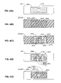
- FIGS. 4(A) , 4 (B), 4 (C), 4 (D) and 4 (E) are plan views depicting stages of a via formation-type patterned structure fabrication process in accordance with another embodiment of the invention.
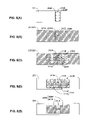
- FIGS. 5(A) , 5 (B), 5 (C), 5 (D) and 5 (E) are plan views depicting stages of a gap formation-type patterned structure fabrication process in accordance with another embodiment of the invention.
- FIGS. 6(A) and 6(B) are side views depicting stages of a gap formation-type patterned structure fabrication process in accordance with another embodiment of the invention.
- FIGS. 7(A) and 7(B) are micrographs showing raised portions of a printed mask produced by underlying lift-off patterns in accordance with an aspect of the present invention
- FIGS. 8(A) , 8 (B), 8 (C), 8 (D), 8 (E), 8 (F), 8 (G), 8 (H), 8 (I), 8 (J), 8 (K), and 8 (L) are side views depicting stages of a TFT fabrication process in accordance with another embodiment of the invention.
- FIGS. 9(A) , 9 (B), 9 (C), 9 (D), 9 (E), 9 (F), 9 (G), 9 (H), 9 (I), 9 (J), 9 (K), and 9 (L) are side views depicting stages of a TFT fabrication process in accordance with yet another embodiment of the invention.
- FIGS. 10(A) and 10(B) are micrographs showing TFT structures at selected stages of the process depicted in FIGS. 9(A) to 9(L) .
- the printed IC pattern typically comprises actual IC features (i.e., elements that will be incorporated into the final IC, such as the gates and source and drain regions of thin film transistors, signal lines, opto-electronic device components, etc.) or a mask for subsequent semiconductor processing (e.g., etch, implant, etc.).
- IC features i.e., elements that will be incorporated into the final IC, such as the gates and source and drain regions of thin film transistors, signal lines, opto-electronic device components, etc.
- a mask for subsequent semiconductor processing e.g., etch, implant, etc.
- the present invention utilizes the pattern printing and lift-off pattern processes of the above-mentioned applications, in combination with standard bulk-processing techniques (e.g., blanket layer formation and wet etching, to generate patterned integrated circuit (IC) structures on a substrate.
- standard bulk-processing techniques e.g., blanket layer formation and wet etching
- the methods of the present invention are utilized to define vias (openings) through patterned structures using a minimum number of etching steps and printing time, thereby facilitating efficient connections between patterned structures of different layers that form an electronic device.
- the methods of the present invention are utilized to fabricate patterned IC structures using pattern printing, bulk processing and lift-off processing that exhibit smaller gaps between features with less overlap between layers.
- the methods of the present invention are utilized to fabricate associated patterned structures formed in two layers (e.g., the gate electrode and source/drain electrodes of a thin-film transistor (TFT)) that minimize or eliminate overlap between the associated patterned structures.
- TFT thin-film transistor
- FIG. 1 is a flow diagram depicting a generalized method according to the present invention for fabricating patterned structures on a substrate such that the patterned structure includes first and second portions that are separated by a void (e.g., a gap or a via (opening)).
- FIGS. 2(A) to 2(E) are cross-sectional side views depicting the method of FIG. 1 in accordance with an exemplary embodiment of the invention.
- the method begins by forming a lift-off pattern in the shape of the desired void over the substrate (block 110 ).
- the lift-off pattern is a sacrificial material that occupies the space ultimately defined by the desired void, and therefore the lift-off pattern is positioned in a predetermined area over, for example, a feature that was previously formed on the substrate.
- a substrate 201 includes a previously formed patterned structure 205 , and a base or intermediate layer 207 (e.g., a blanket dielectric layer) formed over feature 205 .
- Lift-off pattern 210 is the formed on over feature 205 , for example, by wax printing using printing system 300 described below with reference to FIG.
- lift-off pattern 210 may be formed using a resist layer developed using back-side exposure.
- lift-off pattern 210 is deposited using, for example, jet printing, screen printing, gravure, off-set printing, and xerography.
- FIG. 3 is a perspective view of a printing system 300 for printing masks and lift-off patterns (e.g., printed element 210 in FIG. 2(A) ) in accordance with an embodiment of the invention.
- Printing system 300 includes a stage 310 for supporting (and optionally translating) a workpiece 301 (e.g., a substrate or wafer), a print assembly 350 mounted to a printing support structure 380 , and a computer/workstation 390 that serves as both a system controller and data processor.
- Stage 310 includes a rotational platform 312 that allows the orientation of workpiece 301 to be adjusted.
- Optional alignment features 311 on rotational platform 312 can be included to provide gross positioning and capture of workpiece 301 .
- Print assembly 350 includes a print head 330 (on a rotational fixture) and a camera 370 (having high magnification capabilities) mounted in a rigid mount 360 .
- Print head 330 includes one or more ejectors 340 mounted in an ejector base 331 .
- Ejectors 340 are configured to dispense droplets of the appropriate printing fluid on a base layer 320 of workpiece 301 .
- Computer/workstation 390 is configured to receive lift-off pattern and mask data from a data source 391 , and then provide appropriate control signals to printing support structure 380 and stage 310 .
- Data source 391 can comprise any source of lift-off pattern data, including a networked computer, a lift-off pattern database connected via a local area network (LAN) or wide area network (WAN), or even a CD-ROM or other removable storage media.
- the control signals provided by computer/workstation 390 control the motion and printing action of print head 330 as it is translated relative to the base layer 320 .
- Print action can be provided by printing support structure 380 , by stage 310 , or by both in combination. Note further that the printing action does not have to involve actual movement of the print head itself, as print head 330 could be held stationary while stage 310 translates base layer 320 .
- Computer/workstation 390 is also coupled to receive and process imaging data from camera 370 . In one embodiment, camera 370 provides both manual and automated calibration capabilities for printing system 300 .
- the lift-off pattern (e.g., lift-off pattern 210 , FIG. 2(A) ) printed by printing system 300 can be precisely aligned with existing elements in workpiece 301 (e.g., feature 205 , FIG. 2 (A)), thereby ensuring a high-yield manufacturing process.
- system calibration can be accomplished with a video camera microscope (such as camera 370 ) having an optical axis position that is fixed relative to the ejector positions of the print head.
- a video camera microscope such as camera 370
- base layer 207 is depicted as a layer on a substrate 201 for exemplary purposes, according to another embodiment of the invention, lift-off pattern 210 may be formed directly onto a surface of substrate 201 .
- base layer 207 is depicted as a single layer for clarity, according to various other embodiments of the invention, base layer 207 could comprise any number of layers.
- substrate 201 is depicted as a single layer for clarity, according to various other embodiments of the invention, substrate 201 can comprise any number of layers and can include any type of device or structure within those layers.
- lift-off pattern 210 is printed using printing system 300 , described above.
- the printing fluid used to form printed lift-off pattern 210 can comprise a variety of materials, including phase-change materials (e.g., wax, photoresist, and epoxies) and colloidal suspensions (e.g., solution-processable electronic (i.e., conducting, semiconducting, or dielectric materials).
- base layer 207 can comprise any material on which the lift-off pattern can be printed, such as a semiconductor material, a glass plate, or even flexible materials such as fabric or plastics.
- Print lift-off pattern 210 is formed when an ejector of print head 330 ( FIG. 3 ) ejects printing fluid onto base layer 207 .
- the printing fluid attaches itself to base layer 207 through a wetting action and proceeds to solidify in place in a rounded cross-sectional profile.
- the specific size and shape of this profile is guided by competing processes of solidification and wetting.
- solidification occurs when the printed drop loses its thermal energy to the substrate and reverts to a solid form.
- colloidal suspensions such as organic polymers and suspensions of electronic material in a solvent or carrier are printed and wet to the substrate leaving a printed feature.
- the thermal conditions and material properties of the printing fluid and substrate, along with the ambient atmospheric conditions, determine the specific rate at which the deposited printing fluid transforms from a liquid to a solid.
- closely spaced printed elements can be used to create lift-off pattern features that are much smaller than the minimum printed element dimensions.
- a second printed element 215 (indicated by the dotted line) could be printed next to printed lift-off pattern 210 .
- Printed elements 230 and 231 have a minimum width, but may be spaced (edge to edge) by a distance that is smaller than the element width.
- an optional surface treatment is performed on base layer 207 after forming lift-off pattern 210 .
- the surface treatment (such as a clean operation) improves the bonding between base layer 207 and a subsequently deposited blanket layer (described in greater detail below with respect to FIG. 2 (B)), thereby improving the conditions for the eventual lift-off operation.
- the surface treatment can comprise exposing base layer 207 to a plasma etching step (e.g., an oxygen plasma) at room temperature for, e.g., 30 to 120 seconds.
- blanket layer is formed over the substrate and the lift-off pattern (block 120 ).
- blanket 220 is blanket-deposited over base layer 207 and lift-off pattern 210 such that a first portion 221 of blanket layer 220 is formed on base layer 207 and located on a first side of lift-off pattern 210 , a second portion 222 formed on base layer 207 and located on a second (opposite) side of lift-off pattern 210 , and a third portion 223 formed on lift-off pattern 210 .
- blanket layer 220 includes attack points 224 around lift-off pattern 210 .
- Attack points 224 are relatively thin compared to horizontal sections of blanket layer 240 (e.g., sections formed on base layer 207 ), and therefore allow a solvent to penetrate lift-off layer 220 and attack lift-off layer 210 during a subsequent strip operation.
- blanket layer 220 itself can comprise any material that is not significantly affected by the solvent used to strip lift-off pattern 210 .
- lift-off pattern 210 comprises a wax element
- blanket layer 220 could comprise a metal layer (e.g., gold, chromium, or aluminum), an oxide layer, or a semiconductor layer, among others.
- the degree of thinning at attack points 224 depends to a large degree on the profile of lift-off pattern 210 .
- the printing operation parameters e.g., printing material, printing speed
- the printing operation parameters can be adjusted such that the printed lift-off pattern element profile causes actual gaps to be formed in blanket layer 220 , as depicted in FIG. 2(B) .
- a mask is printed onto the blanket layer that overlaps the lift-off pattern and masks the portion of the blanket layer used to form the desired patterned structure (block 230 ).
- structure mask 230 is formed by multiple printed elements 235 that are printed by printing system 300 as described above, and form a substantially unbroken cover over first and second portions 221 and 222 , and over lift-off pattern 210 .
- exposed portions of the blanket layer are then removed, along with the printed structure mask and the lift-off pattern (block 140 ).
- the removal process is performed by wet etching the exposed portions of the blanket layer, followed by a wax removal and/or a lift-off process to remove printed structure mask 230 and lift-off pattern 210 .
- wet etching is performed by applying a suitable etchant 240 to exposed portions of the blanket layer, leaving only portions of the blanket layer that are protected, for example, by printed structure mask 230 (e.g., first portion 221 and second portion 222 ).
- printed structure mask 230 e.g., first portion 221 and second portion 222 .
- nitric acid could be used as etchant 240 during the wet etching process.
- the printed structure mask and lift-off pattern are removed, for example, using a solvent 250 .
- a solvent 250 For example, if printed mask 230 and lift-off pattern 210 comprise wax, and the blanket layer comprises metal, then tetrahydrofuran or toluene could be used as a solvent during the mask removal/lift-off process. Sonication and/or heating may be used to speed up the mask removal/lift-off process.
- patterned structure 225 which includes the retained first portion 221 and second portion 222 separated by void 227 , as shown in FIG. 2(E) .
- First and second portions 221 and 222 of patterned structure 225 therefore have an outer peripheral edge that is substantially the same the printed structure mask, but void 225 has an outer edge that is the inverse of the shape formed by lift-off pattern 210 .
- patterned structure 225 can comprise actual device structures (e.g., contact pads for an IC, electrodes for a transistor device or any other structure in substrate 201 , or bus lines).
- patterned structure 225 can comprise a mask for further processing of base layer 207 .
- patterned structure 225 can serve both as a mask for further processing of base layer 207 , and as an actual device structure.
- FIGS. 4(A) to 4(E) are top plan views showing the formation of a patterned structure 225 A (shown in FIG. 4(E) ) that defines a via (opening) 227 A according to a specific embodiment of the present invention.
- Such vias can be used, for example, to electrically connect the patterned structure to an underlying structure.
- FIGS. 4(A) to 4(E) generally correspond to the processes described above with reference to FIGS. 2A) to 2(E) , respectively, and structures of 4 (A) to 4 (E) are identified with reference numbers that are similar to corresponding structures of FIGS. 2A) to 2(E) .
- FIG. 4(A) shows a substantially dot-like (i.e., substantially one-dimensional) lift-off pattern 210 A that is formed on base layer 207 over feature 205 A.
- blanket layer 220 is formed over base layer 207 , and includes portions 221 A and 222 A formed over corresponding regions of feature 205 A and are generally located on opposite sides of lift-off pattern 210 A.
- FIG. 4(C) shows a printed structure mask 230 A, which is then printed on blanket layer 220 such that printed structure mask 230 A overlaps (covers) lift-off pattern 210 A and is generally aligned with the outer edge of feature 205 A (i.e., such that an outer peripheral edge 231 A (indicated by dashed line) of mask 230 A completely surrounds lift-off pattern 210 A).
- the pattern of mask 230 A is arbitrarily selected for illustrative purposes, and actual mask patterns need not correspond to an underlying feature.
- FIG. 4(D) shows the structure after wet etching has removed exposed portions of the blanket layer surrounding printed mask 230 A, thereby forming a rectangular, island-like patterned structure 225 A including portions 221 A and 222 A, which are located on opposite sides of lift-off pattern 210 A and are linked by portions 223 A that extend around lift-off pattern 210 A between portions 221 A and 222 A.
- FIG. 4(E) shows patterned structure 225 A after mask 230 A and lift-off pattern 210 A are removed, thereby exposing a via 227 A, which is located between first and second portions 221 A and 222 A, and occupies the space previously occupied by the dot-like lift-off pattern.
- via 227 A is positioned over feature 205 A such that via 227 A can be used, for example, to form a metal via connection structure between patterned structure 225 A and feature 205 A in accordance with processes described in co-owned U.S. application Ser. No. 10/741,252 [XCP-038], cited above.
- FIGS. 5(A) to 5(E) are top plan views showing the formation of a patterned structure 225 B (shown in FIG. 5(E) ) that defines a gap 227 B separating spaced-apart portions 221 B and 222 B according to another specific embodiment of the present invention. Such gaps can be used, for example, to form source/drain structures of thin-film transistors (TFTs).
- FIGS. 5(A) to 5(E) generally correspond to the processes described above with reference to FIGS. 2A) to 2(E) , respectively, and structures of 5 (A) to 5 (E) are identified with reference numbers that are similar to corresponding structures of FIGS. 2A) to 2(E) .
- FIGS. 6(A) and 6(B) are side views showing selected stages of the fabrication process that are associated with FIGS. 5(A) and 5(E) , respectively.
- FIGS. 5(A) and 6(A) show an elongated lift-off pattern 210 B that is formed on base layer 207 over a relatively narrow feature 205 B such that elongated lift-off pattern 210 B is aligned with feature 205 B (i.e., the width of elongated lift-off pattern 210 B is substantially equal to feature 205 B, and the peripheral edge 212 B of elongated lift-off pattern 210 B (indicated by dashed line) is generally vertically aligned with a peripheral edge of feature 205 B).
- the width of elongated lift-off pattern 210 B is substantially equal to feature 205 B
- the peripheral edge 212 B of elongated lift-off pattern 210 B is generally vertically aligned with a peripheral edge of feature 205 B.
- blanket layer 220 is formed over base layer 207 , and includes portions 221 B and 222 B formed over corresponding regions of base layer 207 that are generally located on opposite sides of lift-off pattern 210 A.
- FIG. 5(C) shows a printed structure mask 230 B, which is then printed on blanket layer 220 such that printed structure mask 230 B extends across lift-off pattern 210 B such that mask 230 B includes first and second portions that respectively cover first and second portions 221 B and 222 B of blanket layer 220 , where the first and second portions of mask 230 B are separated by elongated lift-off pattern 210 B.
- FIG. 5(D) shows the structure after wet etching has removed exposed portions of the blanket layer surrounding printed mask 230 B, and FIGS.
- 5(E) and 6(E) show patterned structure 225 A after mask 230 A and lift-off pattern 210 A are removed, thereby exposing gap 227 B between spaced-apart portions 221 B and 222 B. Note that opposing outside side edges of gap 227 B (i.e., inside edges of first and second portions 221 B and 222 B) are aligned with outside edges of underlying feature 205 B.
- the printed lift-off pattern can be formed by making multiple printing passes across the same location(s) in the manner set forth in [XC-038], cited above.
- the resulting stacked (multilayer) pattern can then be used to create a patterned lift-off layer having beneficial masking characteristics.
- FIG. 6(A) shows a multi-layer printed lift-off pattern 210 B that is formed from printed elements 211 , 212 and 213 , which are successively printed at the same location during three printing passes, thereby forming the depicted stacked arrangement.
- multi-layer printed lift-off pattern 210 B is described as being formed from three layers for exemplary purposes, according to various embodiments of the invention, any number of layers could be used.
- FIGS. 7(A) and 7(B) are enlarged micrographs (top view) respectively showing printed masks formed over a stacked via-type lift-off pattern ( FIG. 7(A) and a stacked gap-type lift-off pattern ( FIG. 7(B) ).
- the darkened regions in the micrographs show that, although the printed mask is printed over the respective via/gap lift-off pattern, the edges of the via/gap lift-off pattern is not covered by the printed mask, thus facilitating the lift-off process described above.
- patterned structures having vias and gaps using the methods described above may be used to fabricate a wide range of large area electronic structures.
- the via formation method can be used to fabricate solar cells having back-contact architectures where metal electrodes are patterned on the back of a substrate after cell fabrication.
- the resolution needed for this process is very low, typically using line widths of 200 ⁇ m.
- the metal electrodes are deposited on top of a SiO 2 passivation layer. After metal deposition and electrode patterning, a via has to be opened to connect the metal electrodes to the cell.
- the exemplary embodiment described above with reference to FIGS. 4(A) to 4(E) may be used to form the metal electrode with an open via.
- the patterned metal structure can be used as an etch mask for the SiO 2 , enabling the cell to be connected to the outside metal grid.
- the gap formation method can be utilized in the fabrication of TFTs exhibiting minimal source/drain and gate overlap capacitance, where the channel length matches the gate electrode perfectly (e.g., as indicated in FIGS. 5(E) and 6(B) , where feature 205 B is the gate, and patterned structure portions 221 B and 222 B form the source and drain. If the printing process showed a perfect registration from layer to layer, the channel via could be printed in the exact same way as the gate layer, and the device would have no overlap capacitance. However, when the printing registration is on the order of 5 ⁇ m, this offset is enough to reduce transistor performance. One method to avoid this performance reduction is to use the same mask for gates and channel vias.
- the gate layer should be printed at higher temperatures than the channel via layer. Larger gate feature will be obtained by increasing the substrate temperature without the need of printing two pixels for the gate electrode. In this way, the channel length will be more reproducible and the overlap capacitance will be minimized.
- FIGS. 8(A) to 8(L) depict another method for fabricating TFTs that utilizes back-side exposure to self-align the lift-off pattern to the gate structure, which further reduces the overlap between source/drain and gate of a TFT.
- the TFT fabrication process begins by forming a gate structure, which can be formed directly on a substrate 201 or one or more underlying layers, provided the underlying layers are light transparent.
- a gate metal layer 302 is deposited over a substrate 201 (FIG. 8 (A)), and then a gate mask 315 is printed onto a predetermined portion 305 of gate metal layer 302 (indicated by dashed lines in FIG. 8(B) ).
- Gate mask 315 is used in the manner described above to mask a portion of gate metal layer 302 during wet etching, thereby removing exposed portions of the gate metal layer and producing a gate structure 205 C ( FIG. 8(C) ).
- the gate mask is then removed.
- FIGS. 8(D) through 8(H) depict a process for forming a dielectric and a lift-off structure utilized by the TFT according to an aspect of the present embodiment.
- a dielectric layer 207 C is then formed over gate structure 205 C, and then a photoresist layer 321 is formed on dielectric layer 207 C ( FIG. 8(E) ).
- gate structure 205 C is then used as a backside mask to expose portions 322 of the resist layer (i.e., such that gate structure 205 C “shades” a central portion 325 from the radiant energy, which is depicted by dashed arrows 329 ).
- the exposed (second) portions 322 of the photoresist are then removed according to known techniques, whereby central photoresist portion 325 forms a lift-off pattern 210 C.
- the side edges 212 C of lift-off pattern 210 C are substantially self-aligned to the corresponding side edges of gate structure 205 C.
- FIGS. 8(H) to 8(L) depict the formation of source/drain structures separated by a channel gap that is defined by lift-off pattern 210 C using the methods described above.
- a source/drain metal layer 220 C is deposited over lift-off pattern 210 C and exposed portions of dielectric layer 207 C such that source/drain metal layer 220 C includes a first (e.g., source) portion 221 C and a second (e.g., drain) portion 222 C that are respectively located on opposing sides of lift-off pattern 210 C.
- a source/drain mask 230 C is printed using the techniques described above over the first and second portions 221 C and 222 C of source/drain metal layer 220 C, and optionally overlapping lift-off pattern 210 C ( FIG. 8(I) ).
- Etchant 240 is then used to remove portions of the source/drain metal layer exposed by source/drain mask 230 C (FIG. 8 (J)), then the source/drain mask is removed ( FIG. 8(K) , and finally a lift-off process is performed to remove the lift-off pattern, thereby exposing channel gap 227 C between a first (e.g., source) electrode 221 C and second (e.g., drain) electrode 222 C, which are formed on dielectric layer 207 C ( FIG.
- the TFT 300 is completed by deposition and patterning of a semiconducting material island 335 over the channel region. Protective layers and contact electrodes for transmitting signals to the source/drain/gate electrodes are omitted for brevity.
- FIGS. 9(A) to 9(L) depict another method for fabricating TFTs that utilizes an amorphous silicon (a-Si:H)-based bottom gate structure.
- the fabrication process begins by forming a (e.g., chromium) gate structure 205 D on a substrate 201 in a manner similar to that described above.
- a three-layer stack structure 401 is formed over gate structure 205 D that includes an a-Si:H layer 407 sandwiched between two dielectric (e.g., Si 3 N 4 ) layers 402 and 409 .
- dielectric e.g., Si 3 N 4
- FIG. 9(B) a transparent sacrificial layer 410 (e.g., indium-tin oxide (ITO)) is then formed on uppermost dielectric layer 409 , and FIG. 9(C) shows an island mask 420 that is printed on sacrificial layer 410 in a region overlapping gate structure 205 D.
- FIG. 9(D) depicts the structure after the island mask 420 has been used in conjunction with a suitable etchant to remove exposed portions of the sacrificial layer and uppermost dielectric layer, thus forming a sacrificial island 410 D and an underlying dielectric island 409 D, and exposing peripheral portions of a-Si:H layer 407 .
- FIG. 9(E) shows the structure after the island mask has been removed and a blanket photoresist layer 430 is formed on the upper surface of sacrificial island 410 D and the exposed peripheral portions of a-Si:H layer 407 .
- gate structure 205 D is used as a mask to prevent exposure of a portion 435 of the photoresist layer 430 during a backside exposure of (second) portions 432 in a manner similar to that described above.
- FIG. 9(G) shows the structure after the exposed portions of the photoresist layer have been removed using known methods, thereby patterning resist portion 435 such that it is substantially self-aligned to the corresponding side edges of the underlying gate structure 205 D.
- resist portion 435 is then used to remove the exposed portions of the sacrificial island and underlying uppermost dielectric layer, thus forming a lift-off pattern 210 D on a dielectric pattern 409 D 1 , and exposing portions 407 D 1 and 407 D 2 of a-Si:H island 407 D, which are located on opposite sides of lift-off pattern 210 D and are linked by portion 407 D 3 that extends under lift-off pattern 210 D between portions 407 D 1 and 407 D 2 .
- the resist portion located over lift-off pattern 210 D is then removed, and an n+Si layer followed by a source/drain metal layer 440 is then blanket deposited over the entire structure.
- a source/drain mask 450 is then printed on metal layer 440 over a-Si:H island portions 407 D 1 and 407 D 2 , and optionally over lift-off pattern 210 D.
- the exposed portions of metal layer 450 are then etched, and then mask 450 is removed, producing the structure shown in FIG.
- a metal island 440 D including a first (e.g., source) portion 221 D and a second (e.g., drain) portion 222 D that are respectively located on opposing sides of lift-off pattern 210 D, and connected by a third portion 223 D.
- a lift-off process is performed to remove the lift-off pattern in the manner described above, thereby exposing a channel gap 227 D between a first (e.g., source) electrode 221 D and second (e.g., drain) electrode 222 D, which are formed on dielectric layer 207 D (FIG. 9 (L)), essentially completing the fabrication of a TFT 400 (protective layers and contact electrodes for transmitting signals to the source/drain/gate electrodes are omitted for brevity).
- FIGS. 10(A) and 10(B) are micrographs illustrating TFTs formed substantially in accordance with the method described above with reference to FIGS. 9(A) to 9(L) .
- FIG. 10(A) shows the pattern of the s/d contact prior to lift off to the sacrificial layer.
- the self aligned etch mask is a single printed line that crosses over the channel region above the gate electrode. The s/d metal is then etched to define the s/d regions relative to the gate (g) electrode.
- FIG. 10(B) shows the resulting structure after lift-off.
- the resulting TFTs were found to exhibit operating characteristics that were comparable to TFTs produced by standard fabrication methods. Accordingly, the embodiment described with reference to FIGS. 9(A) to 9(L) provide a method in which channel gap 227 D is self-aligned to gate 205 D, thus enabling the production of high quality TFTs for large area electronic devices without requiring the use of lithographic masks.
Abstract
Description
Claims (17)
Priority Applications (1)
| Application Number | Priority Date | Filing Date | Title |
|---|---|---|---|
| US11/184,304 US7459400B2 (en) | 2005-07-18 | 2005-07-18 | Patterned structures fabricated by printing mask over lift-off pattern |
Applications Claiming Priority (1)
| Application Number | Priority Date | Filing Date | Title |
|---|---|---|---|
| US11/184,304 US7459400B2 (en) | 2005-07-18 | 2005-07-18 | Patterned structures fabricated by printing mask over lift-off pattern |
Publications (2)
| Publication Number | Publication Date |
|---|---|
| US20070020883A1 US20070020883A1 (en) | 2007-01-25 |
| US7459400B2 true US7459400B2 (en) | 2008-12-02 |
Family
ID=37679615
Family Applications (1)
| Application Number | Title | Priority Date | Filing Date |
|---|---|---|---|
| US11/184,304 Active 2026-07-07 US7459400B2 (en) | 2005-07-18 | 2005-07-18 | Patterned structures fabricated by printing mask over lift-off pattern |
Country Status (1)
| Country | Link |
|---|---|
| US (1) | US7459400B2 (en) |
Cited By (5)
| Publication number | Priority date | Publication date | Assignee | Title |
|---|---|---|---|---|
| US20100252927A1 (en) * | 2005-07-28 | 2010-10-07 | Palo Alto Research Center Incorporated | Pattern-Print Thin-Film Transistors with Top Gate Geometry |
| US20100304007A1 (en) * | 2008-12-23 | 2010-12-02 | Vipul Dave | Adhesion promoting temporary mask for coated surfaces |
| US8906247B2 (en) | 2012-07-31 | 2014-12-09 | Industrial Technology Research Institute | Patterning process for oxide film |
| US10046584B2 (en) | 2005-12-27 | 2018-08-14 | Palo Alto Research Center Incorporated | Layered structures on thin substrates |
| US10739673B2 (en) | 2014-06-20 | 2020-08-11 | Taiwan Semiconductor Manufacturing Company Limited | Preparing patterned neutral layers and structures prepared using the same |
Families Citing this family (6)
| Publication number | Priority date | Publication date | Assignee | Title |
|---|---|---|---|---|
| US7355225B2 (en) * | 2005-10-26 | 2008-04-08 | Motorola, Inc. | Semiconductor device and method for providing a reduced surface area electrode |
| US7816146B2 (en) * | 2005-12-27 | 2010-10-19 | Palo Alto Research Center Incorporated | Passive electronic devices |
| US7784173B2 (en) * | 2005-12-27 | 2010-08-31 | Palo Alto Research Center Incorporated | Producing layered structures using printing |
| US8318540B2 (en) * | 2008-05-19 | 2012-11-27 | Infineon Technologies Ag | Method of manufacturing a semiconductor structure |
| US20120036308A1 (en) * | 2010-08-06 | 2012-02-09 | Swanson Robert C | Supporting a secure readable memory region for pre-boot and secure mode operations |
| US9373731B2 (en) * | 2011-06-30 | 2016-06-21 | Newsouth Innovations Pty Limited | Dielectric structures in solar cells |
Citations (21)
| Publication number | Priority date | Publication date | Assignee | Title |
|---|---|---|---|---|
| US5521032A (en) * | 1992-02-21 | 1996-05-28 | Hitachi, Ltd. | Exposure mask and method of manufacture thereof |
| US6127725A (en) * | 1998-08-03 | 2000-10-03 | Harris; Ellis D. | Thin film electronics on insulator on metal |
| US6348295B1 (en) * | 1999-03-26 | 2002-02-19 | Massachusetts Institute Of Technology | Methods for manufacturing electronic and electromechanical elements and devices by thin-film deposition and imaging |
| US20030134516A1 (en) * | 2001-04-19 | 2003-07-17 | Palo Alto Research Center Incoporated | Inexpensive fabrication of large-area pixel arrays for displays and sensors |
| US6742884B2 (en) | 2001-04-19 | 2004-06-01 | Xerox Corporation | Apparatus for printing etch masks using phase-change materials |
| US6818959B2 (en) * | 2002-03-12 | 2004-11-16 | Btg International Limited | MEMS devices with voltage driven flexible elements |
| US20050032362A1 (en) * | 2003-05-07 | 2005-02-10 | Microfabrica Inc. | Electrochemical fabrication methods including use of surface treatments to reduce overplating and/or planarization during formation of multi-layer three-dimensional structures |
| US6890050B2 (en) | 2002-08-20 | 2005-05-10 | Palo Alto Research Center Incorporated | Method for the printing of homogeneous electronic material with a multi-ejector print head |
| US20050136358A1 (en) * | 2003-12-19 | 2005-06-23 | Palo Alto Research Center Incorporated | Patterning using wax printing and lift off |
| US6913944B2 (en) * | 2002-12-26 | 2005-07-05 | Konica Minolta Holdings, Inc. | Organic thin-film transistor manufacturing method, organic thin-film transistor, and organic thin-film transistor sheet |
| US20050158880A1 (en) * | 2000-03-17 | 2005-07-21 | President And Fellows Of Harvard College | Cell patterning technique |
| US6972261B2 (en) * | 2002-06-27 | 2005-12-06 | Xerox Corporation | Method for fabricating fine features by jet-printing and surface treatment |
| US20060003475A1 (en) * | 2004-06-30 | 2006-01-05 | Motorola, Inc. | Semiconductor devices shared element(s) apparatus and method |
| US20060105492A1 (en) * | 2002-08-06 | 2006-05-18 | Janos Veres | Organic electronic devices |
| US20060131563A1 (en) * | 2004-12-20 | 2006-06-22 | Palo Alto Research Center Incorporated | Phase-separated composite films and methods of preparing the same |
| US20060131266A1 (en) * | 2004-12-20 | 2006-06-22 | Palo Alto Research Center Incorporated | Large area electronic device with high and low resolution patterned film features |
| US20070026585A1 (en) * | 2005-07-28 | 2007-02-01 | Palo Alto Research Center Incorporated | Patterned-print thin-film transistors with top gate geometry |
| US20070082438A1 (en) * | 2005-10-06 | 2007-04-12 | Seiko Epson Corporation | Thin film transistor and method for fabrication of an electronic device |
| US20070145362A1 (en) * | 2005-12-27 | 2007-06-28 | Palo Alto Research Center Incorporated | Passive electronic devices |
| US20070161163A1 (en) * | 2002-12-26 | 2007-07-12 | Katsura Hirai | Manufacturing method of thin-film transistor, thin-film transistor sheet, and electric circuit |
| US20070166874A1 (en) * | 2004-11-24 | 2007-07-19 | Industrial Technology Research Institute | Fabrication Method of Nanoimprint Mold Core |
-
2005
- 2005-07-18 US US11/184,304 patent/US7459400B2/en active Active
Patent Citations (25)
| Publication number | Priority date | Publication date | Assignee | Title |
|---|---|---|---|---|
| US5521032A (en) * | 1992-02-21 | 1996-05-28 | Hitachi, Ltd. | Exposure mask and method of manufacture thereof |
| US6127725A (en) * | 1998-08-03 | 2000-10-03 | Harris; Ellis D. | Thin film electronics on insulator on metal |
| US6348295B1 (en) * | 1999-03-26 | 2002-02-19 | Massachusetts Institute Of Technology | Methods for manufacturing electronic and electromechanical elements and devices by thin-film deposition and imaging |
| US20050158880A1 (en) * | 2000-03-17 | 2005-07-21 | President And Fellows Of Harvard College | Cell patterning technique |
| US20030134516A1 (en) * | 2001-04-19 | 2003-07-17 | Palo Alto Research Center Incoporated | Inexpensive fabrication of large-area pixel arrays for displays and sensors |
| US6742884B2 (en) | 2001-04-19 | 2004-06-01 | Xerox Corporation | Apparatus for printing etch masks using phase-change materials |
| US6872320B2 (en) | 2001-04-19 | 2005-03-29 | Xerox Corporation | Method for printing etch masks using phase-change materials |
| US6818959B2 (en) * | 2002-03-12 | 2004-11-16 | Btg International Limited | MEMS devices with voltage driven flexible elements |
| US20060057851A1 (en) * | 2002-06-27 | 2006-03-16 | Palo Alto Research Center Incorporated | Method for fabricating fine features by jet-printing and surface treatment |
| US6972261B2 (en) * | 2002-06-27 | 2005-12-06 | Xerox Corporation | Method for fabricating fine features by jet-printing and surface treatment |
| US20060105492A1 (en) * | 2002-08-06 | 2006-05-18 | Janos Veres | Organic electronic devices |
| US6890050B2 (en) | 2002-08-20 | 2005-05-10 | Palo Alto Research Center Incorporated | Method for the printing of homogeneous electronic material with a multi-ejector print head |
| US20050142293A1 (en) * | 2002-08-20 | 2005-06-30 | Palo Alto Research Center Incorporated | Method for the printing of homogeneous electronic material with a multi-ejector print head |
| US20070161163A1 (en) * | 2002-12-26 | 2007-07-12 | Katsura Hirai | Manufacturing method of thin-film transistor, thin-film transistor sheet, and electric circuit |
| US6913944B2 (en) * | 2002-12-26 | 2005-07-05 | Konica Minolta Holdings, Inc. | Organic thin-film transistor manufacturing method, organic thin-film transistor, and organic thin-film transistor sheet |
| US20050032362A1 (en) * | 2003-05-07 | 2005-02-10 | Microfabrica Inc. | Electrochemical fabrication methods including use of surface treatments to reduce overplating and/or planarization during formation of multi-layer three-dimensional structures |
| US7109118B2 (en) * | 2003-05-07 | 2006-09-19 | Microfabrica Inc. | Electrochemical fabrication methods including use of surface treatments to reduce overplating and/or planarization during formation of multi-layer three-dimensional structures |
| US20050136358A1 (en) * | 2003-12-19 | 2005-06-23 | Palo Alto Research Center Incorporated | Patterning using wax printing and lift off |
| US20060003475A1 (en) * | 2004-06-30 | 2006-01-05 | Motorola, Inc. | Semiconductor devices shared element(s) apparatus and method |
| US20070166874A1 (en) * | 2004-11-24 | 2007-07-19 | Industrial Technology Research Institute | Fabrication Method of Nanoimprint Mold Core |
| US20060131563A1 (en) * | 2004-12-20 | 2006-06-22 | Palo Alto Research Center Incorporated | Phase-separated composite films and methods of preparing the same |
| US20060131266A1 (en) * | 2004-12-20 | 2006-06-22 | Palo Alto Research Center Incorporated | Large area electronic device with high and low resolution patterned film features |
| US20070026585A1 (en) * | 2005-07-28 | 2007-02-01 | Palo Alto Research Center Incorporated | Patterned-print thin-film transistors with top gate geometry |
| US20070082438A1 (en) * | 2005-10-06 | 2007-04-12 | Seiko Epson Corporation | Thin film transistor and method for fabrication of an electronic device |
| US20070145362A1 (en) * | 2005-12-27 | 2007-06-28 | Palo Alto Research Center Incorporated | Passive electronic devices |
Non-Patent Citations (1)
| Title |
|---|
| Thomasson D.B., "Fully Self-Aligned Tri-layer a-Si:H Thin-Film Transistors with Deposited Doped Contact Layer" IEEE Electron Device Letters, vol. 19, No. 4 1998 p. 124-126. * |
Cited By (8)
| Publication number | Priority date | Publication date | Assignee | Title |
|---|---|---|---|---|
| US20100252927A1 (en) * | 2005-07-28 | 2010-10-07 | Palo Alto Research Center Incorporated | Pattern-Print Thin-Film Transistors with Top Gate Geometry |
| US7884361B2 (en) | 2005-07-28 | 2011-02-08 | Palo Alto Research Center Incorporated | Pattern-print thin-film transistors with top gate geometry |
| US10046584B2 (en) | 2005-12-27 | 2018-08-14 | Palo Alto Research Center Incorporated | Layered structures on thin substrates |
| US20100304007A1 (en) * | 2008-12-23 | 2010-12-02 | Vipul Dave | Adhesion promoting temporary mask for coated surfaces |
| US8927049B2 (en) * | 2008-12-23 | 2015-01-06 | Cordis Corporation | Adhesion promoting temporary mask for coated surfaces |
| US8906247B2 (en) | 2012-07-31 | 2014-12-09 | Industrial Technology Research Institute | Patterning process for oxide film |
| US10739673B2 (en) | 2014-06-20 | 2020-08-11 | Taiwan Semiconductor Manufacturing Company Limited | Preparing patterned neutral layers and structures prepared using the same |
| US11226555B2 (en) | 2014-06-20 | 2022-01-18 | Taiwan Semiconductor Manufacturing Company Limited | Preparing patterned neutral layers and structures prepared using the same |
Also Published As
| Publication number | Publication date |
|---|---|
| US20070020883A1 (en) | 2007-01-25 |
Similar Documents
| Publication | Publication Date | Title |
|---|---|---|
| US7459400B2 (en) | Patterned structures fabricated by printing mask over lift-off pattern | |
| JP5296303B2 (en) | Electrical component manufacturing method and electrical component structure | |
| US9614102B2 (en) | Self-aligned metal oxide TFT with reduced number of masks and with reduced power consumption | |
| US6746904B2 (en) | Electronic devices comprising thin film transistors | |
| KR100803426B1 (en) | Substrate and process for producing the same | |
| US6495386B2 (en) | Method of manufacturing an active matrix device | |
| US7816193B2 (en) | Method for fabricating a pixel structure of a liquid crystal display | |
| JP6073880B2 (en) | Method for forming top gate type transistor | |
| CN100452304C (en) | Method for producing film transistor and lower substrate for LCD | |
| JP2002268585A (en) | Active matrix substrate and method for manufacturing the same | |
| US7629206B2 (en) | Patterning self-aligned transistors using back surface illumination | |
| US7148090B2 (en) | Method of fabricating a TFT device formed by printing | |
| TW594349B (en) | Liquid crystal display device and method of the same | |
| JPH02273935A (en) | Manufacture of thin film transistor | |
| JP5200408B2 (en) | Thin film transistor manufacturing method | |
| KR20010038188A (en) | a manufacturing method of a thin film transistor panel for a liquid crystal display | |
| KR20050097172A (en) | Method of fabricating array substrate for liquid crystal display device | |
| JPH01250929A (en) | Manufacture of thin film transistor panel | |
| TW201021217A (en) | Bottom substrate of liquid crystal display | |
| JP2000114533A (en) | Manufacture of semiconductor device | |
| JPH0713194A (en) | Liquid crystal display device and its production |
Legal Events
| Date | Code | Title | Description |
|---|---|---|---|
| AS | Assignment |
Owner name: PALO ALTO RESEARCH CENTER INCORPORATED, CALIFORNIA Free format text: ASSIGNMENT OF ASSIGNORS INTEREST;ASSIGNORS:ARIAS, ANA C.;LUJAN, RENE A.;WONG, WILLIAM S.;REEL/FRAME:016791/0659 Effective date: 20050715 |
|
| FEPP | Fee payment procedure |
Free format text: PAYOR NUMBER ASSIGNED (ORIGINAL EVENT CODE: ASPN); ENTITY STATUS OF PATENT OWNER: LARGE ENTITY |
|
| STCF | Information on status: patent grant |
Free format text: PATENTED CASE |
|
| FPAY | Fee payment |
Year of fee payment: 4 |
|
| CC | Certificate of correction | ||
| FPAY | Fee payment |
Year of fee payment: 8 |
|
| FEPP | Fee payment procedure |
Free format text: MAINTENANCE FEE REMINDER MAILED (ORIGINAL EVENT CODE: REM.); ENTITY STATUS OF PATENT OWNER: LARGE ENTITY |
|
| FEPP | Fee payment procedure |
Free format text: 11.5 YR SURCHARGE- LATE PMT W/IN 6 MO, LARGE ENTITY (ORIGINAL EVENT CODE: M1556); ENTITY STATUS OF PATENT OWNER: LARGE ENTITY |
|
| MAFP | Maintenance fee payment |
Free format text: PAYMENT OF MAINTENANCE FEE, 12TH YEAR, LARGE ENTITY (ORIGINAL EVENT CODE: M1553); ENTITY STATUS OF PATENT OWNER: LARGE ENTITY Year of fee payment: 12 |
|
| AS | Assignment |
Owner name: XEROX CORPORATION, CONNECTICUT Free format text: ASSIGNMENT OF ASSIGNORS INTEREST;ASSIGNOR:PALO ALTO RESEARCH CENTER INCORPORATED;REEL/FRAME:064038/0001 Effective date: 20230416 |
|
| AS | Assignment |
Owner name: CITIBANK, N.A., AS COLLATERAL AGENT, NEW YORK Free format text: SECURITY INTEREST;ASSIGNOR:XEROX CORPORATION;REEL/FRAME:064760/0389 Effective date: 20230621 |
|
| AS | Assignment |
Owner name: XEROX CORPORATION, CONNECTICUT Free format text: CORRECTIVE ASSIGNMENT TO CORRECT THE REMOVAL OF US PATENTS 9356603, 10026651, 10626048 AND INCLUSION OF US PATENT 7167871 PREVIOUSLY RECORDED ON REEL 064038 FRAME 0001. ASSIGNOR(S) HEREBY CONFIRMS THE ASSIGNMENT;ASSIGNOR:PALO ALTO RESEARCH CENTER INCORPORATED;REEL/FRAME:064161/0001 Effective date: 20230416 |
|
| AS | Assignment |
Owner name: JEFFERIES FINANCE LLC, AS COLLATERAL AGENT, NEW YORK Free format text: SECURITY INTEREST;ASSIGNOR:XEROX CORPORATION;REEL/FRAME:065628/0019 Effective date: 20231117 |
|
| AS | Assignment |
Owner name: CITIBANK, N.A., AS COLLATERAL AGENT, NEW YORK Free format text: SECURITY INTEREST;ASSIGNOR:XEROX CORPORATION;REEL/FRAME:066741/0001 Effective date: 20240206 |