US7430656B2 - System and method of converting data formats and communicating between execution units - Google Patents
System and method of converting data formats and communicating between execution units Download PDFInfo
- Publication number
- US7430656B2 US7430656B2 US10/334,114 US33411402A US7430656B2 US 7430656 B2 US7430656 B2 US 7430656B2 US 33411402 A US33411402 A US 33411402A US 7430656 B2 US7430656 B2 US 7430656B2
- Authority
- US
- United States
- Prior art keywords
- execution unit
- exception
- format
- data
- internal format
- Prior art date
- Legal status (The legal status is an assumption and is not a legal conclusion. Google has not performed a legal analysis and makes no representation as to the accuracy of the status listed.)
- Expired - Fee Related, expires
Links
- 238000000034 method Methods 0.000 title claims abstract description 14
- 230000015654 memory Effects 0.000 claims description 17
- 238000012545 processing Methods 0.000 claims description 11
- 238000006243 chemical reaction Methods 0.000 description 34
- 238000012546 transfer Methods 0.000 description 8
- 238000010586 diagram Methods 0.000 description 6
- 230000005540 biological transmission Effects 0.000 description 3
- 238000004590 computer program Methods 0.000 description 2
- 238000012986 modification Methods 0.000 description 2
- 230000004048 modification Effects 0.000 description 2
- 238000011022 operating instruction Methods 0.000 description 2
- 230000003287 optical effect Effects 0.000 description 2
- 230000008569 process Effects 0.000 description 2
- 238000012360 testing method Methods 0.000 description 2
- 230000009471 action Effects 0.000 description 1
- 238000013459 approach Methods 0.000 description 1
- 230000008901 benefit Effects 0.000 description 1
- 238000004891 communication Methods 0.000 description 1
- 238000013461 design Methods 0.000 description 1
- 230000008439 repair process Effects 0.000 description 1
- 239000007787 solid Substances 0.000 description 1
- 230000003068 static effect Effects 0.000 description 1
- 238000006467 substitution reaction Methods 0.000 description 1
- 238000013519 translation Methods 0.000 description 1
Images


Classifications
-
- G—PHYSICS
- G06—COMPUTING; CALCULATING OR COUNTING
- G06F—ELECTRIC DIGITAL DATA PROCESSING
- G06F9/00—Arrangements for program control, e.g. control units
- G06F9/06—Arrangements for program control, e.g. control units using stored programs, i.e. using an internal store of processing equipment to receive or retain programs
- G06F9/30—Arrangements for executing machine instructions, e.g. instruction decode
- G06F9/30003—Arrangements for executing specific machine instructions
- G06F9/30007—Arrangements for executing specific machine instructions to perform operations on data operands
- G06F9/3001—Arithmetic instructions
- G06F9/30014—Arithmetic instructions with variable precision
-
- G—PHYSICS
- G06—COMPUTING; CALCULATING OR COUNTING
- G06F—ELECTRIC DIGITAL DATA PROCESSING
- G06F9/00—Arrangements for program control, e.g. control units
- G06F9/06—Arrangements for program control, e.g. control units using stored programs, i.e. using an internal store of processing equipment to receive or retain programs
- G06F9/22—Microcontrol or microprogram arrangements
- G06F9/226—Microinstruction function, e.g. input/output microinstruction; diagnostic microinstruction; microinstruction format
-
- G—PHYSICS
- G06—COMPUTING; CALCULATING OR COUNTING
- G06F—ELECTRIC DIGITAL DATA PROCESSING
- G06F9/00—Arrangements for program control, e.g. control units
- G06F9/06—Arrangements for program control, e.g. control units using stored programs, i.e. using an internal store of processing equipment to receive or retain programs
- G06F9/30—Arrangements for executing machine instructions, e.g. instruction decode
- G06F9/30003—Arrangements for executing specific machine instructions
- G06F9/30007—Arrangements for executing specific machine instructions to perform operations on data operands
- G06F9/30025—Format conversion instructions, e.g. Floating-Point to Integer, decimal conversion
-
- G—PHYSICS
- G06—COMPUTING; CALCULATING OR COUNTING
- G06F—ELECTRIC DIGITAL DATA PROCESSING
- G06F9/00—Arrangements for program control, e.g. control units
- G06F9/06—Arrangements for program control, e.g. control units using stored programs, i.e. using an internal store of processing equipment to receive or retain programs
- G06F9/30—Arrangements for executing machine instructions, e.g. instruction decode
- G06F9/30003—Arrangements for executing specific machine instructions
- G06F9/30007—Arrangements for executing specific machine instructions to perform operations on data operands
- G06F9/30036—Instructions to perform operations on packed data, e.g. vector, tile or matrix operations
-
- G—PHYSICS
- G06—COMPUTING; CALCULATING OR COUNTING
- G06F—ELECTRIC DIGITAL DATA PROCESSING
- G06F9/00—Arrangements for program control, e.g. control units
- G06F9/06—Arrangements for program control, e.g. control units using stored programs, i.e. using an internal store of processing equipment to receive or retain programs
- G06F9/30—Arrangements for executing machine instructions, e.g. instruction decode
- G06F9/3017—Runtime instruction translation, e.g. macros
-
- G—PHYSICS
- G06—COMPUTING; CALCULATING OR COUNTING
- G06F—ELECTRIC DIGITAL DATA PROCESSING
- G06F9/00—Arrangements for program control, e.g. control units
- G06F9/06—Arrangements for program control, e.g. control units using stored programs, i.e. using an internal store of processing equipment to receive or retain programs
- G06F9/30—Arrangements for executing machine instructions, e.g. instruction decode
- G06F9/38—Concurrent instruction execution, e.g. pipeline, look ahead
- G06F9/3824—Operand accessing
- G06F9/3826—Bypassing or forwarding of data results, e.g. locally between pipeline stages or within a pipeline stage
-
- G—PHYSICS
- G06—COMPUTING; CALCULATING OR COUNTING
- G06F—ELECTRIC DIGITAL DATA PROCESSING
- G06F9/00—Arrangements for program control, e.g. control units
- G06F9/06—Arrangements for program control, e.g. control units using stored programs, i.e. using an internal store of processing equipment to receive or retain programs
- G06F9/30—Arrangements for executing machine instructions, e.g. instruction decode
- G06F9/38—Concurrent instruction execution, e.g. pipeline, look ahead
- G06F9/3861—Recovery, e.g. branch miss-prediction, exception handling
Definitions
- New computer chip architectures may be developed to increase processing speed and accuracy.
- a chip architecture there may be a tradeoff between the speed of normal execution and exception handling.
- exception handling may be done in hardware, micro-code, or a combination thereof.
- processors may use packed data formats and SIMD (single instruction-stream, multiple data-stream) instruction sets.
- FIG. 1 is a block diagram illustration of an architectural format and an internal format of a packed double number, in accordance with an embodiment of the present invention
- FIG. 2 is a figurative illustration of possible layers in a processor, in an embodiment of the present invention.
- FIG. 3 is a data flow illustration of normal data transfer between elements of a processor, in an embodiment of the present invention.
- FIG. 4 is a data flow illustration of exception data transfer in the processor of FIG. 3 , in an embodiment of the present invention.
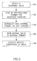
- FIG. 5 is a flow chart diagram of exception handling when a denormal value is input to a first execution unit, in accordance with an embodiment of the present invention.
- FIG. 6 is a flow chart diagram of exception handling when an underflow result is created by a first execution unit, in accordance with an embodiment of the present invention.
- Embodiments of the present invention may include apparatus for performing the operations herein.
- This apparatus may be specially constructed for the desired purposes, or it may comprise a general-purpose computer selectively activated or reconfigured by a computer program stored in the computer.
- a computer program may be stored in a computer readable storage medium, such as, but not limited to, any type of disk, including floppy disks, optical disks, magnetic-optical disks, read-only memories (ROMs), compact disc read-only memories (CD-ROMs), random access memories (RAMs), electrically programmable read-only memories (EPROMs), electrically erasable and programmable read only memories (EEPROMs), Flash, magnetic or optical cards, or any other type of media suitable for storing electronic instructions and capable of being coupled to a computer system bus.
- ROMs read-only memories
- CD-ROMs compact disc read-only memories
- RAMs random access memories
- EPROMs electrically programmable read-only memories
- EEPROMs electrically erasable and programm
- normal operation indicates operation in which no underflow or denormal values are generated or input, values that may cause an exception to be raised.
- architectural format includes memory format as well.
- the term includes all formats used in normal operation to store data in the processor's memory or register file. It includes the formats normally used to transfer data.
- internal format includes formats that may be used internally by an execution unit. Different execution units may use different formats.
- FIG. 1 a block diagram illustration of an architectural format and an internal format of a packed double number, in accordance with an embodiment of the present invention.
- An architectural packed double number (labeled 5 ) may comprise, for example, 128 contiguous bits, wherein one number (labeled 10 A) is stored in bits 127 - 64 , and a second number (labeled 10 B) is stored in bits 63 - 0 .
- the two numbers 10 A and 10 B may be stored, for example, in two contignous 64-bit segments.
- each number may be expanded from 64 bits to 86 bits creating two separate numbers 20 A and 20 B.
- ISA instruction set architecture
- SSETM streaming SIMD extension
- SSE2TM streaming SIMD extension
- a smaller format may allow fewer significant bits in a result, bits which may be needed for exception handling or in representing an intermediate result.
- two common exception conditions may be denormal numbers and underflow, which may be caused by intermediate results that may require a wider foliate for resolution.
- Two other number types used in an arithmetic execution unit may be packed single and packed integer, which may also have corresponding internal formats.
- a packed single may comprise, for example, four 32 bit numbers whose corresponding wider internal formats may comprise, for example, one 79 bit or two 39 bit segments.
- a packed integer number (also referred to as a vector integer) may comprise, for example, any of sixteen 8-bit, eight 16-bit, or four 32-bit numbers in the 128 bits of the architectural format.
- the corresponding internal format may remain the same size, for a total of 128 bits.
- FIG. 2 is a figurative illustration of possible layers in a processor, in an embodiment of the present invention, wherein the innermost circle may reflect the lowest level or layer in the processor architecture and the outermost circle may reflect the highest architectural level.
- the innermost layer may be comprised of at least one execution unit 22 .
- the next layer may be comprised of a bypass network 24 which may be used to transmit data between execution units 22 .
- a chip register file 26 may comprise the next level, wherein register formats may be stored.
- the highest layer may be memory 28 , which may comprise, for example, RAM (random access memory) or cache.
- RAM may further comprise, for example, static RAM (S-RAM) and dynamic RAM (D-RAM).
- Each circle, 23 A, 23 B, 23 C, 25 , and 27 may symbolize the boundary between the adjacent layers.
- boundary circles 23 A, 23 B, and 23 C may depict the boundary between execution units 22 A, 22 B, and 22 C (reflectively) and bypass network 24 .
- a boundary circle 25 may reflect the boundary between bypass network 24 and chip register file 26
- a boundary circle 27 may reflect the boundary between chip register file 26 and memory 28 .
- data used in arithmetic execution units may be in internal format
- data in non-arithmetic execution units, register file 26 , and memory 28 may be stored in the possibly smaller architectural format.
- it may be necessity at some point to convert the data from internal format to architectural format and vice versa. This may depend on which data format may be represented in the intermediary levels bypass network 24 and chip register file 26 .
- data conversion may generally occur between execution unit 22 and bypass network 24 when execution unit 22 uses the internal format. This will be further discussed hereinbelow with respect to FIGS. 3 and 4 .
- the smaller architectural format may be used in all of the levels from bypass network 24 to memory 28 , including chip register file 26 , which may result in a savings in complexity and space on the chip.
- non-arithmetic execution units 22 may remain in architectural format. Arithmetic execution units 22 performing integer operations, for example, may generally not require the extra precision of the internal format as the result size may always correspond to the input data size. However, arithmetic execution units 22 may require the extra precision afforded by use of the internal format during the course of floating point operations, for example, during floating point addition and multiplication.
- intermediate data may be stored in register file 26 and/or memory 28 in the wider internal format.
- the formal result may be stored in architectural format.
- it may still be necessary at some point to convert the data from internal format to architectural format and vice versa.
- it may be necessary to have a different procedure and/or control for when the data conversion may occur.
- a non-typed architecture may be used, wherein a given register may load any instruction of any type and data may be freely transferred between macroinstructions of any type.
- the same set of architectural registers may be used for all data types and operations (for example, packed single, packed double, packed integer, and logical operation) as they may all comprise the same number of bits.
- all registers in the register file may actually be big enough to store the maximum sized internal format value. For example, all registers may be 86 bits wide, which may be the size of one packed double word in internal format. Thus, any register may be able to store any architectural value in only 64 bits of the register. Any internal format number may also be stored, however, the number of bits used may be different for each data type.
- a processor may comprise an arithmetic execution unit 32 , a non-arithmetic execution unit 34 , a conversion unit 36 associated with arithmetic execution unit 32 , and connectivity layer 38 .
- Connectivity layer 38 may comprise interfaces to any data cache or out of order (OOO) logic unit, for example a reorder buffer (ROB) or reservation station (RS) buffer.
- OOO out of order
- ROB reorder buffer
- RS reservation station
- Any data input (or output) to (or from) arithmetic execution unit 32 may first pass through conversion unit 36 , which may comprise the actual interface with the other elements.
- Data transfer between any of arithmetic execution unit 32 (via conversion unit 36 ), non-arithmetic execution unit 34 , and connectivity layer 38 may be in architectural format (as shown by the data flow arrows).
- Conversion when necessary may be performed by conversion unit 36 as data is passed in or out of arithmetic execution unit 32 .
- Conversion unit 36 may physically be a part of arithmetic execution unit 32 or may be operatively associated with arithmetic execution unit 32 .
- assembler macroinstructions may be converted into a flow of microinstruction, which may be executed by the execution units.
- a microinstruction may comprise, for example, all operation code, a target register, and ail operation type. The operation type may be based on the data type expected by the operation.
- Micro code refers to a long sequence of microinstructions.
- data may be transmitted between execution units 32 in an architectural, format. It is understood, that the transmission between execution units may in fact comprise entering and leaving an execution unit 32 via a conversion unit 36 as explained further hereinabove.
- the data received in the architectural format may be converted to an internal format based on the operation code and the operation type of a given microinstruction. Conversion may comprise determining the operation code and the type associated with the operation and translating the data received by conversion unit 36 . The conversion may allow the representation of a wider intermediate result during execution of the microinstruction. Conversion may also be performed from the internal format to the memory format when the operation is complete.
- This data flow wherein all conversions may be done on entry/exit from/to arithmetic execution unit 32 , may save time since conversions may be done immediately. It may not be necessary to pass data out to higher architectural layers such as the register file for conversion when data is produced in one type and transferred into ail execution unit that consumes a different type. Furthermore, no special procedures may be necessary in instructions receiving mixed data types.
- this data flow may comprise a method of communicating in an architectural format between executions units on an integrated circuit, wherein the execution units may operate on and/or produce different data types.
- This communication method may comprise converting a number that is in an architectural format to a number in an internal format before entry to an execution unit, if required by the operating instruction, and converting the result from a number in internal format to a number in architectural format on exit from the execution unit.
- exception handling data may be transmitted between execution units 32 in an architectural format or an internal format. It is understood, that the transmission between execution units may in fact comprise entering and leaving an execution unit 32 via a conversion unit 36 as explained further hereinabove. Whether conversion should be performed may be managed based on either a microinstruction type or an exception type. These conversion management decisions may override the data conversions that may be performed during normal operation and may execute exception handling micro code.
- an operation set may exist for each data type.
- data type is not enforced.
- a packed single number may be transformed into its log value by using a packed integer execution unit such as a shifter unit to perform a shift operation and may thus save space and reduce complexity.
- FIG. 4 is a data flow illustration of exception data transfer in the processor of FIG. 3 , in an embodiment of the present invention.
- arithmetic execution unit 32 arithmetic execution unit 32
- non-arithmetic execution unit 34 conversion unit 36 associated with arithmetic execution unit 32
- connectivity layer 38 arithmetic execution unit 32
- data transfer between any of arithmetic execution unit 32 (via conversion unit 36 ), non-arithmetic execution unit 34 , and connectivity layer 38 may be in architectural format (as shown by the solid data flow arrows). Conversion when necessary may be performed by conversion unit 36 as data is passed in or out of arithmetic execution unit 32 .
- data transfer between arithmetic execution unit 32 and connectivity layer 38 may also be in internal format (as shown by the dashed data flow arrows).
- underflow results and denormal data input may require special handling. If it is possible to deal with these conditions directly in the hardware, it may not be necessary to raise an “exception” and incur the time penalty that may be caused by the use of special exception handling micro code.
- the hardware of the existing multiplication and addition execution units may not currently contain the capability to resolve these cases, it may be necessary to add additional hardware. For example, it may be necessary to add clocks for repairing the operation and chip space for the repairing logic itself. This may cause performance problems and may require special code coverage testing.
- such hardware may not be added; instead micro code may be invoked to handle the exception cases and may use existing logic to do the repair.
- the use of a wider internal format may allow the representation of underflow results without the loss of precision.
- the internal format may comprise a greater number of bits, it may be possible to save an underflow result as a denormal number in the architectural format, as explained hereinbelow. It may also be possible in internal format, to represent a number that in architectural format is a denormal value, as a normal floating point number due to the wider format.
- conversion logic 36 may be instructed not to convert a value. For example, no conversion may occur when a repaired denormal value that is represented in internal format is received as an input or when an underflow has been created as an output. In these cases, the values may be represented in the internal format. In these cases, the data may be sent to an appropriate arithmetic execution unit 32 without conversion being performed by conversion unit 36 and the value may be fixed as instructed by the micro code.
- An embodiment of the present invention may not fix underflow in hardware as this may require a more complex rounder, which may be able to perform a massive right shift.
- an adder unit may comprise the circuitry to perform a massive right shift operation
- the micro code may instruct the adder unit to perform the operation instead. This may save both in the complexity of the rounder unit and the performance of coverage checks of a new, more complicated rounder.
- the architecture of the present invention may use untyped data.
- the data may comprise no identity information.
- An exception may be raised by the setting of a flag, for example, underflow.
- the micro code may determine the data type, as the micro code may know which operation faulted and the data type information may be present in the operation instruction code.
- the micro code may denormalize the value; it may shift the mantissa of the result and may set the exponent to zero.
- the case of a denormal value input may be determined by the presence of a zero exponent and a non-zero mantissa. It may be possible to normalize the denormal value when converted to the wider internal format such that the first “1” in the mantissa is shifted right and the exponent is increased accordingly.
- forward operations may have been performed on data that may raise an exception.
- the inclusion of these erroneous results may be prevented by the retirement logic.
- a denormal value may be detected by a first execution unit and an exception may be raised (stage 100 ).
- the denormal number may be sent in architectural format to an appropriate, possibly different, execution unit for handling (stage 102 ).
- the appropriate execution unit may normalize the number into an internal format value but may instruct the converter not to convert the normal number back to architectural format on exit from the appropriate execution unit (stage 104 ).
- the value, now a normal number in internal format may be transmitted to the register file and then back to the first execution unit in internal format (stage 106 ).
- the first execution unit may execute its operations without converting the internal format input value (stage 108 ), processing may continue as appropriate, and the result may generally be in architectural format.
- FIG. 6 is a flow chart diagram of exception handling when an underflow result is created by a first execution unit, in accordance with an embodiment of the present invention.
- the first execution unit may detect an underflow result (stage 120 ).
- the result in internal format, may be output without conversion or rounding and stored in the register file (stage 122 ).
- the result may be sent to an appropriate, possibly different, execution unit to be denormalized in architectural format (stage 124 ).
- the result may be stored in a register file in architectural format as a denormal value (stage 126 ).
- the denormal value may be input to the next operation execution unit (stage 128 ).
Abstract
Description
Claims (10)
Priority Applications (1)
| Application Number | Priority Date | Filing Date | Title |
|---|---|---|---|
| US10/334,114 US7430656B2 (en) | 2002-12-31 | 2002-12-31 | System and method of converting data formats and communicating between execution units |
Applications Claiming Priority (1)
| Application Number | Priority Date | Filing Date | Title |
|---|---|---|---|
| US10/334,114 US7430656B2 (en) | 2002-12-31 | 2002-12-31 | System and method of converting data formats and communicating between execution units |
Publications (2)
| Publication Number | Publication Date |
|---|---|
| US20040128486A1 US20040128486A1 (en) | 2004-07-01 |
| US7430656B2 true US7430656B2 (en) | 2008-09-30 |
Family
ID=32654933
Family Applications (1)
| Application Number | Title | Priority Date | Filing Date |
|---|---|---|---|
| US10/334,114 Expired - Fee Related US7430656B2 (en) | 2002-12-31 | 2002-12-31 | System and method of converting data formats and communicating between execution units |
Country Status (1)
| Country | Link |
|---|---|
| US (1) | US7430656B2 (en) |
Cited By (55)
| Publication number | Priority date | Publication date | Assignee | Title |
|---|---|---|---|---|
| US20070038693A1 (en) * | 2005-08-10 | 2007-02-15 | Christian Jacobi | Method and Processor for Performing a Floating-Point Instruction Within a Processor |
| US20080148011A1 (en) * | 2006-12-14 | 2008-06-19 | Intel Corporation | Carry/Borrow Handling |
| US20080256523A1 (en) * | 2007-04-12 | 2008-10-16 | Nancy Grimaldi | Computerized Data Warehousing |
| US20090198977A1 (en) * | 2008-01-31 | 2009-08-06 | Gschwind Michael K | Sharing Data in Internal and Memory Representations with Dynamic Data-Driven Conversion |
| US20090198966A1 (en) * | 2008-01-31 | 2009-08-06 | Gschwind Michael K | Multi-Addressable Register File |
| US20090327665A1 (en) * | 2008-06-30 | 2009-12-31 | Zeev Sperber | Efficient parallel floating point exception handling in a processor |
| US20100095099A1 (en) * | 2008-10-14 | 2010-04-15 | International Business Machines Corporation | System and method for storing numbers in first and second formats in a register file |
| US20100100713A1 (en) * | 2008-10-22 | 2010-04-22 | International Business Machines Corporation | Fast floating point compare with slower backup for corner cases |
| US7822799B1 (en) | 2006-06-26 | 2010-10-26 | Altera Corporation | Adder-rounder circuitry for specialized processing block in programmable logic device |
| US7836117B1 (en) | 2006-04-07 | 2010-11-16 | Altera Corporation | Specialized processing block for programmable logic device |
| US7865541B1 (en) * | 2007-01-22 | 2011-01-04 | Altera Corporation | Configuring floating point operations in a programmable logic device |
| US7930336B2 (en) | 2006-12-05 | 2011-04-19 | Altera Corporation | Large multiplier for programmable logic device |
| US7948267B1 (en) | 2010-02-09 | 2011-05-24 | Altera Corporation | Efficient rounding circuits and methods in configurable integrated circuit devices |
| US7949699B1 (en) | 2007-08-30 | 2011-05-24 | Altera Corporation | Implementation of decimation filter in integrated circuit device using ram-based data storage |
| US8041759B1 (en) | 2006-02-09 | 2011-10-18 | Altera Corporation | Specialized processing block for programmable logic device |
| US8266199B2 (en) | 2006-02-09 | 2012-09-11 | Altera Corporation | Specialized processing block for programmable logic device |
| US8266198B2 (en) | 2006-02-09 | 2012-09-11 | Altera Corporation | Specialized processing block for programmable logic device |
| US8301681B1 (en) | 2006-02-09 | 2012-10-30 | Altera Corporation | Specialized processing block for programmable logic device |
| US8307023B1 (en) | 2008-10-10 | 2012-11-06 | Altera Corporation | DSP block for implementing large multiplier on a programmable integrated circuit device |
| US8386553B1 (en) | 2006-12-05 | 2013-02-26 | Altera Corporation | Large multiplier for programmable logic device |
| US8386550B1 (en) | 2006-09-20 | 2013-02-26 | Altera Corporation | Method for configuring a finite impulse response filter in a programmable logic device |
| US8396914B1 (en) | 2009-09-11 | 2013-03-12 | Altera Corporation | Matrix decomposition in an integrated circuit device |
| US8412756B1 (en) | 2009-09-11 | 2013-04-02 | Altera Corporation | Multi-operand floating point operations in a programmable integrated circuit device |
| US8468192B1 (en) | 2009-03-03 | 2013-06-18 | Altera Corporation | Implementing multipliers in a programmable integrated circuit device |
| US8484265B1 (en) | 2010-03-04 | 2013-07-09 | Altera Corporation | Angular range reduction in an integrated circuit device |
| US8510354B1 (en) | 2010-03-12 | 2013-08-13 | Altera Corporation | Calculation of trigonometric functions in an integrated circuit device |
| US8539016B1 (en) | 2010-02-09 | 2013-09-17 | Altera Corporation | QR decomposition in an integrated circuit device |
| US8539014B2 (en) | 2010-03-25 | 2013-09-17 | Altera Corporation | Solving linear matrices in an integrated circuit device |
| US8543634B1 (en) | 2012-03-30 | 2013-09-24 | Altera Corporation | Specialized processing block for programmable integrated circuit device |
| US8577951B1 (en) | 2010-08-19 | 2013-11-05 | Altera Corporation | Matrix operations in an integrated circuit device |
| US8589463B2 (en) | 2010-06-25 | 2013-11-19 | Altera Corporation | Calculation of trigonometric functions in an integrated circuit device |
| US8601044B2 (en) | 2010-03-02 | 2013-12-03 | Altera Corporation | Discrete Fourier Transform in an integrated circuit device |
| US8620980B1 (en) | 2005-09-27 | 2013-12-31 | Altera Corporation | Programmable device with specialized multiplier blocks |
| US8645450B1 (en) | 2007-03-02 | 2014-02-04 | Altera Corporation | Multiplier-accumulator circuitry and methods |
| US8645451B2 (en) | 2011-03-10 | 2014-02-04 | Altera Corporation | Double-clocked specialized processing block in an integrated circuit device |
| US8645449B1 (en) | 2009-03-03 | 2014-02-04 | Altera Corporation | Combined floating point adder and subtractor |
| US8650236B1 (en) | 2009-08-04 | 2014-02-11 | Altera Corporation | High-rate interpolation or decimation filter in integrated circuit device |
| US8650231B1 (en) | 2007-01-22 | 2014-02-11 | Altera Corporation | Configuring floating point operations in a programmable device |
| US8706790B1 (en) | 2009-03-03 | 2014-04-22 | Altera Corporation | Implementing mixed-precision floating-point operations in a programmable integrated circuit device |
| US8762443B1 (en) | 2011-11-15 | 2014-06-24 | Altera Corporation | Matrix operations in an integrated circuit device |
| US8812576B1 (en) | 2011-09-12 | 2014-08-19 | Altera Corporation | QR decomposition in an integrated circuit device |
| US8862650B2 (en) | 2010-06-25 | 2014-10-14 | Altera Corporation | Calculation of trigonometric functions in an integrated circuit device |
| US8949298B1 (en) | 2011-09-16 | 2015-02-03 | Altera Corporation | Computing floating-point polynomials in an integrated circuit device |
| US8959137B1 (en) | 2008-02-20 | 2015-02-17 | Altera Corporation | Implementing large multipliers in a programmable integrated circuit device |
| US8996600B1 (en) | 2012-08-03 | 2015-03-31 | Altera Corporation | Specialized processing block for implementing floating-point multiplier with subnormal operation support |
| US9053045B1 (en) | 2011-09-16 | 2015-06-09 | Altera Corporation | Computing floating-point polynomials in an integrated circuit device |
| US9098332B1 (en) | 2012-06-01 | 2015-08-04 | Altera Corporation | Specialized processing block with fixed- and floating-point structures |
| US9189200B1 (en) | 2013-03-14 | 2015-11-17 | Altera Corporation | Multiple-precision processing block in a programmable integrated circuit device |
| US9207909B1 (en) | 2012-11-26 | 2015-12-08 | Altera Corporation | Polynomial calculations optimized for programmable integrated circuit device structures |
| US9348795B1 (en) | 2013-07-03 | 2016-05-24 | Altera Corporation | Programmable device using fixed and configurable logic to implement floating-point rounding |
| US9395981B2 (en) | 2011-09-16 | 2016-07-19 | International Business Machines Corporation | Multi-addressable register files and format conversions associated therewith |
| US9600278B1 (en) | 2011-05-09 | 2017-03-21 | Altera Corporation | Programmable device using fixed and configurable logic to implement recursive trees |
| US9684488B2 (en) | 2015-03-26 | 2017-06-20 | Altera Corporation | Combined adder and pre-adder for high-radix multiplier circuit |
| US9727336B2 (en) | 2011-09-16 | 2017-08-08 | International Business Machines Corporation | Fine-grained instruction enablement at sub-function granularity based on an indicated subrange of registers |
| US10942706B2 (en) | 2017-05-05 | 2021-03-09 | Intel Corporation | Implementation of floating-point trigonometric functions in an integrated circuit device |
Families Citing this family (2)
| Publication number | Priority date | Publication date | Assignee | Title |
|---|---|---|---|---|
| CN105630467B (en) * | 2014-10-31 | 2020-07-14 | 腾讯科技(武汉)有限公司 | Rendering processing method and processing device for user interaction interface |
| JP6951622B2 (en) * | 2017-05-18 | 2021-10-20 | 富士通株式会社 | Arithmetic processing unit and control method of arithmetic processing unit |
Citations (7)
| Publication number | Priority date | Publication date | Assignee | Title |
|---|---|---|---|---|
| US5652862A (en) * | 1992-12-30 | 1997-07-29 | Apple Computer, Inc. | Method and appartus for determining a precision of an intermediate arithmetic for converting values between a first numeric format and a second numeric format |
| US5768169A (en) | 1995-10-02 | 1998-06-16 | Intel Corporation | Method and apparatus for improved processing of numeric applications in the presence of subnormal numbers in a computer system |
| US6002393A (en) * | 1995-08-22 | 1999-12-14 | Hite; Kenneth C. | System and method for delivering targeted advertisements to consumers using direct commands |
| US6219780B1 (en) * | 1998-10-27 | 2001-04-17 | International Business Machines Corporation | Circuit arrangement and method of dispatching instructions to multiple execution units |
| US6321327B1 (en) | 1998-12-30 | 2001-11-20 | Intel Corporation | Method for setting a bit associated with each component of packed floating-pint operand that is normalized in SIMD operations |
| US20040128331A1 (en) * | 2002-12-27 | 2004-07-01 | Hinds Christopher N. | Data processing apparatus and method for converting a number between fixed-point and floating-point representations |
| US6829627B2 (en) * | 2001-01-18 | 2004-12-07 | International Business Machines Corporation | Floating point unit for multiple data architectures |
-
2002
- 2002-12-31 US US10/334,114 patent/US7430656B2/en not_active Expired - Fee Related
Patent Citations (7)
| Publication number | Priority date | Publication date | Assignee | Title |
|---|---|---|---|---|
| US5652862A (en) * | 1992-12-30 | 1997-07-29 | Apple Computer, Inc. | Method and appartus for determining a precision of an intermediate arithmetic for converting values between a first numeric format and a second numeric format |
| US6002393A (en) * | 1995-08-22 | 1999-12-14 | Hite; Kenneth C. | System and method for delivering targeted advertisements to consumers using direct commands |
| US5768169A (en) | 1995-10-02 | 1998-06-16 | Intel Corporation | Method and apparatus for improved processing of numeric applications in the presence of subnormal numbers in a computer system |
| US6219780B1 (en) * | 1998-10-27 | 2001-04-17 | International Business Machines Corporation | Circuit arrangement and method of dispatching instructions to multiple execution units |
| US6321327B1 (en) | 1998-12-30 | 2001-11-20 | Intel Corporation | Method for setting a bit associated with each component of packed floating-pint operand that is normalized in SIMD operations |
| US6829627B2 (en) * | 2001-01-18 | 2004-12-07 | International Business Machines Corporation | Floating point unit for multiple data architectures |
| US20040128331A1 (en) * | 2002-12-27 | 2004-07-01 | Hinds Christopher N. | Data processing apparatus and method for converting a number between fixed-point and floating-point representations |
Non-Patent Citations (1)
| Title |
|---|
| IEEE Standard for Binary Floating-Point Arithmetic. * |
Cited By (68)
| Publication number | Priority date | Publication date | Assignee | Title |
|---|---|---|---|---|
| US20070038693A1 (en) * | 2005-08-10 | 2007-02-15 | Christian Jacobi | Method and Processor for Performing a Floating-Point Instruction Within a Processor |
| US8620980B1 (en) | 2005-09-27 | 2013-12-31 | Altera Corporation | Programmable device with specialized multiplier blocks |
| US8266199B2 (en) | 2006-02-09 | 2012-09-11 | Altera Corporation | Specialized processing block for programmable logic device |
| US8266198B2 (en) | 2006-02-09 | 2012-09-11 | Altera Corporation | Specialized processing block for programmable logic device |
| US8041759B1 (en) | 2006-02-09 | 2011-10-18 | Altera Corporation | Specialized processing block for programmable logic device |
| US8301681B1 (en) | 2006-02-09 | 2012-10-30 | Altera Corporation | Specialized processing block for programmable logic device |
| US7836117B1 (en) | 2006-04-07 | 2010-11-16 | Altera Corporation | Specialized processing block for programmable logic device |
| US7822799B1 (en) | 2006-06-26 | 2010-10-26 | Altera Corporation | Adder-rounder circuitry for specialized processing block in programmable logic device |
| US8386550B1 (en) | 2006-09-20 | 2013-02-26 | Altera Corporation | Method for configuring a finite impulse response filter in a programmable logic device |
| US9063870B1 (en) | 2006-12-05 | 2015-06-23 | Altera Corporation | Large multiplier for programmable logic device |
| US8788562B2 (en) | 2006-12-05 | 2014-07-22 | Altera Corporation | Large multiplier for programmable logic device |
| US8386553B1 (en) | 2006-12-05 | 2013-02-26 | Altera Corporation | Large multiplier for programmable logic device |
| US9395953B2 (en) | 2006-12-05 | 2016-07-19 | Altera Corporation | Large multiplier for programmable logic device |
| US7930336B2 (en) | 2006-12-05 | 2011-04-19 | Altera Corporation | Large multiplier for programmable logic device |
| US20080148011A1 (en) * | 2006-12-14 | 2008-06-19 | Intel Corporation | Carry/Borrow Handling |
| US8650231B1 (en) | 2007-01-22 | 2014-02-11 | Altera Corporation | Configuring floating point operations in a programmable device |
| US7865541B1 (en) * | 2007-01-22 | 2011-01-04 | Altera Corporation | Configuring floating point operations in a programmable logic device |
| US8645450B1 (en) | 2007-03-02 | 2014-02-04 | Altera Corporation | Multiplier-accumulator circuitry and methods |
| US8191053B2 (en) * | 2007-04-12 | 2012-05-29 | Ingenix, Inc. | Computerized data warehousing |
| US20080256523A1 (en) * | 2007-04-12 | 2008-10-16 | Nancy Grimaldi | Computerized Data Warehousing |
| US7949699B1 (en) | 2007-08-30 | 2011-05-24 | Altera Corporation | Implementation of decimation filter in integrated circuit device using ram-based data storage |
| US7877582B2 (en) | 2008-01-31 | 2011-01-25 | International Business Machines Corporation | Multi-addressable register file |
| US20090198966A1 (en) * | 2008-01-31 | 2009-08-06 | Gschwind Michael K | Multi-Addressable Register File |
| US7849294B2 (en) * | 2008-01-31 | 2010-12-07 | International Business Machines Corporation | Sharing data in internal and memory representations with dynamic data-driven conversion |
| US20090198977A1 (en) * | 2008-01-31 | 2009-08-06 | Gschwind Michael K | Sharing Data in Internal and Memory Representations with Dynamic Data-Driven Conversion |
| US8959137B1 (en) | 2008-02-20 | 2015-02-17 | Altera Corporation | Implementing large multipliers in a programmable integrated circuit device |
| US8103858B2 (en) * | 2008-06-30 | 2012-01-24 | Intel Corporation | Efficient parallel floating point exception handling in a processor |
| US20090327665A1 (en) * | 2008-06-30 | 2009-12-31 | Zeev Sperber | Efficient parallel floating point exception handling in a processor |
| US9092226B2 (en) | 2008-06-30 | 2015-07-28 | Intel Corporation | Efficient parallel floating point exception handling in a processor |
| US8307023B1 (en) | 2008-10-10 | 2012-11-06 | Altera Corporation | DSP block for implementing large multiplier on a programmable integrated circuit device |
| US8346828B2 (en) * | 2008-10-14 | 2013-01-01 | International Business Machines Corporation | System and method for storing numbers in first and second formats in a register file |
| US20100095099A1 (en) * | 2008-10-14 | 2010-04-15 | International Business Machines Corporation | System and method for storing numbers in first and second formats in a register file |
| US8407275B2 (en) | 2008-10-22 | 2013-03-26 | International Business Machines Corporation | Fast floating point compare with slower backup for corner cases |
| US20100100713A1 (en) * | 2008-10-22 | 2010-04-22 | International Business Machines Corporation | Fast floating point compare with slower backup for corner cases |
| US8706790B1 (en) | 2009-03-03 | 2014-04-22 | Altera Corporation | Implementing mixed-precision floating-point operations in a programmable integrated circuit device |
| US8645449B1 (en) | 2009-03-03 | 2014-02-04 | Altera Corporation | Combined floating point adder and subtractor |
| US8468192B1 (en) | 2009-03-03 | 2013-06-18 | Altera Corporation | Implementing multipliers in a programmable integrated circuit device |
| US8650236B1 (en) | 2009-08-04 | 2014-02-11 | Altera Corporation | High-rate interpolation or decimation filter in integrated circuit device |
| US8412756B1 (en) | 2009-09-11 | 2013-04-02 | Altera Corporation | Multi-operand floating point operations in a programmable integrated circuit device |
| US8396914B1 (en) | 2009-09-11 | 2013-03-12 | Altera Corporation | Matrix decomposition in an integrated circuit device |
| US8539016B1 (en) | 2010-02-09 | 2013-09-17 | Altera Corporation | QR decomposition in an integrated circuit device |
| US7948267B1 (en) | 2010-02-09 | 2011-05-24 | Altera Corporation | Efficient rounding circuits and methods in configurable integrated circuit devices |
| US8601044B2 (en) | 2010-03-02 | 2013-12-03 | Altera Corporation | Discrete Fourier Transform in an integrated circuit device |
| US8484265B1 (en) | 2010-03-04 | 2013-07-09 | Altera Corporation | Angular range reduction in an integrated circuit device |
| US8510354B1 (en) | 2010-03-12 | 2013-08-13 | Altera Corporation | Calculation of trigonometric functions in an integrated circuit device |
| US8539014B2 (en) | 2010-03-25 | 2013-09-17 | Altera Corporation | Solving linear matrices in an integrated circuit device |
| US8589463B2 (en) | 2010-06-25 | 2013-11-19 | Altera Corporation | Calculation of trigonometric functions in an integrated circuit device |
| US8862650B2 (en) | 2010-06-25 | 2014-10-14 | Altera Corporation | Calculation of trigonometric functions in an integrated circuit device |
| US8812573B2 (en) | 2010-06-25 | 2014-08-19 | Altera Corporation | Calculation of trigonometric functions in an integrated circuit device |
| US8577951B1 (en) | 2010-08-19 | 2013-11-05 | Altera Corporation | Matrix operations in an integrated circuit device |
| US8645451B2 (en) | 2011-03-10 | 2014-02-04 | Altera Corporation | Double-clocked specialized processing block in an integrated circuit device |
| US9600278B1 (en) | 2011-05-09 | 2017-03-21 | Altera Corporation | Programmable device using fixed and configurable logic to implement recursive trees |
| US8812576B1 (en) | 2011-09-12 | 2014-08-19 | Altera Corporation | QR decomposition in an integrated circuit device |
| US9395981B2 (en) | 2011-09-16 | 2016-07-19 | International Business Machines Corporation | Multi-addressable register files and format conversions associated therewith |
| US9727337B2 (en) | 2011-09-16 | 2017-08-08 | International Business Machines Corporation | Fine-grained instruction enablement at sub-function granularity based on an indicated subrange of registers |
| US9053045B1 (en) | 2011-09-16 | 2015-06-09 | Altera Corporation | Computing floating-point polynomials in an integrated circuit device |
| US8949298B1 (en) | 2011-09-16 | 2015-02-03 | Altera Corporation | Computing floating-point polynomials in an integrated circuit device |
| US9727336B2 (en) | 2011-09-16 | 2017-08-08 | International Business Machines Corporation | Fine-grained instruction enablement at sub-function granularity based on an indicated subrange of registers |
| US9411585B2 (en) | 2011-09-16 | 2016-08-09 | International Business Machines Corporation | Multi-addressable register files and format conversions associated therewith |
| US8762443B1 (en) | 2011-11-15 | 2014-06-24 | Altera Corporation | Matrix operations in an integrated circuit device |
| US8543634B1 (en) | 2012-03-30 | 2013-09-24 | Altera Corporation | Specialized processing block for programmable integrated circuit device |
| US9098332B1 (en) | 2012-06-01 | 2015-08-04 | Altera Corporation | Specialized processing block with fixed- and floating-point structures |
| US8996600B1 (en) | 2012-08-03 | 2015-03-31 | Altera Corporation | Specialized processing block for implementing floating-point multiplier with subnormal operation support |
| US9207909B1 (en) | 2012-11-26 | 2015-12-08 | Altera Corporation | Polynomial calculations optimized for programmable integrated circuit device structures |
| US9189200B1 (en) | 2013-03-14 | 2015-11-17 | Altera Corporation | Multiple-precision processing block in a programmable integrated circuit device |
| US9348795B1 (en) | 2013-07-03 | 2016-05-24 | Altera Corporation | Programmable device using fixed and configurable logic to implement floating-point rounding |
| US9684488B2 (en) | 2015-03-26 | 2017-06-20 | Altera Corporation | Combined adder and pre-adder for high-radix multiplier circuit |
| US10942706B2 (en) | 2017-05-05 | 2021-03-09 | Intel Corporation | Implementation of floating-point trigonometric functions in an integrated circuit device |
Also Published As
| Publication number | Publication date |
|---|---|
| US20040128486A1 (en) | 2004-07-01 |
Similar Documents
| Publication | Publication Date | Title |
|---|---|---|
| US7430656B2 (en) | System and method of converting data formats and communicating between execution units | |
| US6108772A (en) | Method and apparatus for supporting multiple floating point processing models | |
| US4918594A (en) | Method and system for logical simulation of information processing system including logic circuit model and logic function model | |
| US5917741A (en) | Method and apparatus for performing floating-point rounding operations for multiple precisions using incrementers | |
| US8880815B2 (en) | Low access time indirect memory accesses | |
| EP0399757B1 (en) | Paired instruction processor precise exception handling mechanism | |
| US5805475A (en) | Load-store unit and method of loading and storing single-precision floating-point registers in a double-precision architecture | |
| JP2000235491A (en) | Processing of load error of computer processor | |
| EP0399760A2 (en) | Paired instruction processor branch recovery mechanism | |
| EP2666067B1 (en) | Device and method for computing a function value of a function | |
| US10248488B2 (en) | Fault tolerance and detection by replication of input data and evaluating a packed data execution result | |
| WO1998025201A1 (en) | Method and apparatus for selecting a rounding mode for a numeric operation | |
| US10228956B2 (en) | Supporting binary translation alias detection in an out-of-order processor | |
| US4295203A (en) | Automatic rounding of floating point operands | |
| US3699326A (en) | Rounding numbers expressed in 2{40 s complement notation | |
| US4528640A (en) | Method and a means for checking normalizing operations in a computer device | |
| US7523152B2 (en) | Methods for supporting extended precision integer divide macroinstructions in a processor | |
| KR20210028075A (en) | System to perform unary functions using range-specific coefficient sets | |
| US6219684B1 (en) | Optimized rounding in underflow handlers | |
| WO2017119973A1 (en) | Binary translation support using processor instruction prefixes | |
| US20030018936A1 (en) | High integrity cache directory | |
| US7237096B1 (en) | Storing results of producer instructions to facilitate consumer instruction dependency tracking | |
| US8825727B2 (en) | Software-hardware adder | |
| US5612909A (en) | Method and apparatus for rounding operands using previous rounding history | |
| US7165172B1 (en) | Facilitating cold reset and warm reset tasking in a computer system |
Legal Events
| Date | Code | Title | Description |
|---|---|---|---|
| AS | Assignment |
Owner name: INTEL CORPORATION, CALIFORNIA Free format text: ASSIGNMENT OF ASSIGNORS INTEREST;ASSIGNORS:SPERBER, ZEEV;ANATI, ITTAI;LIRON, ODED;AND OTHERS;REEL/FRAME:013934/0914;SIGNING DATES FROM 20030205 TO 20030228 |
|
| STCF | Information on status: patent grant |
Free format text: PATENTED CASE |
|
| FEPP | Fee payment procedure |
Free format text: PAYER NUMBER DE-ASSIGNED (ORIGINAL EVENT CODE: RMPN); ENTITY STATUS OF PATENT OWNER: LARGE ENTITY Free format text: PAYOR NUMBER ASSIGNED (ORIGINAL EVENT CODE: ASPN); ENTITY STATUS OF PATENT OWNER: LARGE ENTITY |
|
| FPAY | Fee payment |
Year of fee payment: 4 |
|
| FPAY | Fee payment |
Year of fee payment: 8 |
|
| FEPP | Fee payment procedure |
Free format text: MAINTENANCE FEE REMINDER MAILED (ORIGINAL EVENT CODE: REM.); ENTITY STATUS OF PATENT OWNER: LARGE ENTITY |
|
| LAPS | Lapse for failure to pay maintenance fees |
Free format text: PATENT EXPIRED FOR FAILURE TO PAY MAINTENANCE FEES (ORIGINAL EVENT CODE: EXP.); ENTITY STATUS OF PATENT OWNER: LARGE ENTITY |
|
| STCH | Information on status: patent discontinuation |
Free format text: PATENT EXPIRED DUE TO NONPAYMENT OF MAINTENANCE FEES UNDER 37 CFR 1.362 |
|
| FP | Lapsed due to failure to pay maintenance fee |
Effective date: 20200930 |