US7423275B2 - Erosion mitigation for collector optics using electric and magnetic fields - Google Patents
Erosion mitigation for collector optics using electric and magnetic fields Download PDFInfo
- Publication number
- US7423275B2 US7423275B2 US10/759,344 US75934404A US7423275B2 US 7423275 B2 US7423275 B2 US 7423275B2 US 75934404 A US75934404 A US 75934404A US 7423275 B2 US7423275 B2 US 7423275B2
- Authority
- US
- United States
- Prior art keywords
- magnetic field
- collector optics
- reflective surface
- collector
- field generator
- Prior art date
- Legal status (The legal status is an assumption and is not a legal conclusion. Google has not performed a legal analysis and makes no representation as to the accuracy of the status listed.)
- Expired - Fee Related, expires
Links
Images


Classifications
-
- G—PHYSICS
- G03—PHOTOGRAPHY; CINEMATOGRAPHY; ANALOGOUS TECHNIQUES USING WAVES OTHER THAN OPTICAL WAVES; ELECTROGRAPHY; HOLOGRAPHY
- G03F—PHOTOMECHANICAL PRODUCTION OF TEXTURED OR PATTERNED SURFACES, e.g. FOR PRINTING, FOR PROCESSING OF SEMICONDUCTOR DEVICES; MATERIALS THEREFOR; ORIGINALS THEREFOR; APPARATUS SPECIALLY ADAPTED THEREFOR
- G03F7/00—Photomechanical, e.g. photolithographic, production of textured or patterned surfaces, e.g. printing surfaces; Materials therefor, e.g. comprising photoresists; Apparatus specially adapted therefor
- G03F7/70—Microphotolithographic exposure; Apparatus therefor
- G03F7/708—Construction of apparatus, e.g. environment aspects, hygiene aspects or materials
- G03F7/70908—Hygiene, e.g. preventing apparatus pollution, mitigating effect of pollution or removing pollutants from apparatus
- G03F7/70916—Pollution mitigation, i.e. mitigating effect of contamination or debris, e.g. foil traps
-
- H—ELECTRICITY
- H01—ELECTRIC ELEMENTS
- H01L—SEMICONDUCTOR DEVICES NOT COVERED BY CLASS H10
- H01L21/00—Processes or apparatus adapted for the manufacture or treatment of semiconductor or solid state devices or of parts thereof
- H01L21/02—Manufacture or treatment of semiconductor devices or of parts thereof
- H01L21/027—Making masks on semiconductor bodies for further photolithographic processing not provided for in group H01L21/18 or H01L21/34
- H01L21/0271—Making masks on semiconductor bodies for further photolithographic processing not provided for in group H01L21/18 or H01L21/34 comprising organic layers
- H01L21/0273—Making masks on semiconductor bodies for further photolithographic processing not provided for in group H01L21/18 or H01L21/34 comprising organic layers characterised by the treatment of photoresist layers
Definitions
- Lithography is used in the fabrication of semiconductor devices.
- a light sensitive material called a “photoresist” coats a wafer substrate, such as silicon.
- the photoresist may be exposed to light reflected from a mask to reproduce an image of the mask.
- the photoresist undergoes chemical reactions and is then developed to produce a replicated pattern of the mask on the wafer.
- EUV lithography is a promising future lithography technique.
- EUV light may be produced using a small, hot plasma that will efficiently radiate at a desired wavelength, e.g., in a range of approximately 11 nm to 15 nm.
- the plasma may be created in a vacuum chamber, typically by driving a pulsed electrical discharge through the target material or by focusing a pulsed laser beam onto the target material.
- the light produced by the plasma is then collected by nearby mirrors and sent downstream to the rest of the lithography tool.
- the hot plasma tends to erode materials nearby, e.g., the electrodes in electric discharge sources.
- the eroded material may coat the collector optics, resulting in a loss of reflectivity and reducing the amount of light available for lithography.
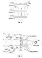
- FIG. 1 is a block diagram of a lithography system.
- FIG. 2 is a sectional view of a light source chamber.
- FIG. 3 is a sectional view of a light source chamber including a magnetic field generator in a Discharge Produced Plasma (DPP) system.
- DPP Discharge Produced Plasma
- FIG. 4A is a side view of a magnetic field generator for collector optics.
- FIG. 4B illustrates the effect of a magnetic field on debris particles.
- FIG. 5 is a sectional view of a light source chamber including a magnetic field generator in a Laser Produced Plasma (LPP) system.
- LPP Laser Produced Plasma
- FIG. 6A is a perspective view of nested collector optics and illustrates the effect of a generate magnetic field on a debris particle.
- FIG. 6B is an end view of the nested collector optics and magnetic field of FIG. 6A .
- FIG. 7A is a perspective view of nested collector optics with a magnetic field generator according to another embodiment.
- FIG. 7B illustrates a dipole field generated by a wire in the nested collector optics of FIG. 7B .
- FIG. 8 is a sectional view of nested collector optics with a magnetic field generator according to another embodiment.
- FIG. 9 is a perspective view of a light source chamber including collector optics and a foil trap to trap debris.
- FIG. 1 shows a lithography system 100 .
- a wafer, coated with a light sensitive coating (“photoresist”), and a mask may be placed in a lithography chamber 105 .
- the pressure in the lithography chamber 105 may be reduced to a near vacuum environment by vacuum pumps 110 .
- a light source chamber 115 which houses a light source, is connected to the lithography chamber 105 .
- the pressure in the light source chamber may also be reduced to a near vacuum environment by the vacuum pumps 110 .
- the light source chamber and lithography chamber may be separated by a valve 120 which may be used to isolate the chambers. This allows for different environments within the different chambers.
- the light source chamber 115 may be an EUV chamber, which houses an EUV light source.
- a power supply 125 is connected to the EUV chamber to supply energy for creating an EUV photon emitting plasma, which provides EUV light for lithography.
- the EUV light may have a wavelength in a range of 11 nm to 15 nm, e.g., 13.5 nm.
- the source may be a plasma light source, e.g., a laser plasma source or a pinch plasma source. Plasma-producing components, such as electrodes, in the EUV source may excite a gas, such as Xenon, to produce EUV radiation.
- the EUV chamber may be evacuated by the vacuum pumps 110 .
- FIG. 2 shows a sectional view of an exemplary EUV chamber.
- the light source in this case a discharge produced plasma (DPP) source 205 , and collector mirrors 210 for collecting and directing the EUV light 215 for use in the lithography chamber 105 are inside the EUV chamber.
- the collector mirrors 210 may have a nominally conical/cylindrical structure.
- Tungsten (W) or other refractory metals or alloys that are resistant to plasma erosion may be used for components in the EUV source. However, plasma-erosion may still occur, and the debris produced by the erosion may be deposited on the collector mirrors 210 . Debris may be produced from other sources, e.g., the walls of the chamber. Debris particles may coat the collector mirrors, resulting in a loss of reflectivity. Fast atoms produced by the electric discharge (e.g., Xe, Li, Sn, or In) may sputter away part of the collector mirror surfaces, further reducing reflectivity.
- the electric discharge e.g., Xe, Li, Sn, or In
- a magnetic field is created around the collector mirrors to deflect charged particles and/or highly energetic ions 220 and thereby reduce erosion.
- a magnetic field may be generated using a solenoid structure. This magnetic field may be used to generate Lorentz force when there is a charged particle traveling perpendicular or at certain other angles with respect to the magnetic field direction.
- I high current
- FIG. 3 shows an exemplary arrangement including a magnetic field generator 405 added in the collector optics.
- FIG. 4A is enlarged view of a single collector element with the magnetic field generator.
- the magnetic field generator includes a ferromagnetic core 510 and a coil 520 with many loops to improve the field strength.
- High velocity particles or ions 530 may be deflected away from the surface of the collector optics by the magnetic field 540 as shown in FIG. 4B , thereby reducing any sputtering or erosion of the surface material.
- a cooling system may be included around to the solenoid structure for thermal management.
- a magnetic field generator 570 may be implemented in a laser produced plasma (LPP) system.
- LPP laser produced plasma
- the collector optics may have a nested shell arrangement, as shown in FIGS. 6A and 6B .
- the collector optics may include an inner shell 602 , and outer shell 604 , with one or more intervening shells 606 .
- Each of the shells may have a reflective inner surface (i.e., facing toward the center of the shell structure) and a non-reflective backside.
- An azimuthal magnetic field 608 may be produced by passing a current down the length of the inner and outer shells 602 , 604 , or alternatively, separate extra-thick shells concentric with the actual reflective shells. Such a field would then act to carry a positively charged ion 610 towards the non-reflective backside of each collector shell.
- inner and outer current-carrying shells (coaxial with the reflective shells) of 1 cm thick copper are provided.
- the outer shell has a radius of 10 cm and a cross-sectional area (2 pi r dr) of approximately 6000 cm 2 , and a length of 20 cm.
- HVM high volume manufacturing
- Such energies may cover the vast majority of ions discharged from typical EUV sources.
- the small minority with energies of several keV might be slowed to 500 eV or less by the time they reach the collector section by introducing a buffer gas.
- a series of insulated wires 702 are wrapped around the outside of each shell, thus avoiding any blockage of the light, as shown in FIG. 7A .
- the wires 702 may be charged to a potential while the shells are held to a ground 704 . Near one of the wires, the presence of the grounded plane results in a dipole field 710 , as shown in FIG. 7B .
- the strong gradients present in the dipole field may serve to collect even neutrally charged particles.
- each collector shell may be split into two conducting layers, which are separated by an insulator 802 , as shown in FIG. 8 .
- the reflective layer 804 is charged to a positive state and the non-reflective side 806 to a negative state. This creates an electric field 808 pointing away from each reflective surface 804 , and towards the backing of the neighboring shell.
- This approach may work particularly well for positively charged ions, carrying them away from the reflective surfaces and towards the non-reflective surfaces.
- Positively charged ions are known to be one of the primary sources of damage of the collectors. However, this may not work as well for neutrals as the field gradient would be relatively weak.
- wire and split-plate approaches described above in connection with FIGS. 7A and 8 may be combined in various ways.
- a split-plate approach may be used for a section of the collector nearest the light source and wires may be applied to a section farthest from the light source.
- wires or bumps may be placed on the non-reflective collector side to introduce larger field gradients and thus increase the capture rate neutrals.
- electret fibers may be used instead of wires connected to a power supply. Electret fibers are permanently imbued with an electric dipole moment. Electret fibers are commercially available, and are produced by the mature process of polymer melt-blowing with either corona charging or electrostatic fiber spinning.
- the fibers are continuously released in liquid state out of a die into a region of a strong electric field. After some distance the fiber crystallizes with the electric field embedded in it. Fiber thickness can reach below 1 micron, although 100 microns is used in the present description for mechanical reliability.
- the backside surface of each collector may be grooved or textured to assist collecting any particles that are drawn to the surface.
- either charged wires or electret fibers could be attached perpendicularly between the shells, forming a web that would attract particles.
- a disadvantage to this approach is that some light would be absorbed and fast particles may make it through the web. However, negatively charged particles would be attracted to the reflective surface, making this approach favorable if such particles were in the minority.
- debris-contaminant “foil traps”, e.g., foil elements 902 may be positioned between the source 205 and the collector mirrors 210 , as shown in FIG. 9 .
- the foil elements may be small, thin foils spaced apart from each other by, e.g., 1 mm and spaced apart from the source by, e.g., 10-20 mm.
- the debris particles travel in a jagged path characteristic of Brownian motion. This path makes the debris particles susceptible to striking, and being captured by, the foil traps.
- the outer and inner current-carrying shells may extend towards the foil trap and thus extend the magnetic field into the trap.
- the thinly spaced foils may capture ions only slightly deflected, giving the magnetic field more time to act on an ion.
- the magnetic field may be enhanced by incorporating ferrous materials into the various components.
Abstract
Description
R=?L/A=2·10−8*0.2 m/6·10−3 m2˜6.6·10−3?.
Current: I=sqrt(P/R)=sqrt(1 kW/6.6·10−3 ?)=39 kA.
B˜? 0 I/4?r=1.26·10−6??m*3.9·104 A/(4?*0.1 m)=0.04 T
R=mV/qB->V=qBR/m=1.6·10−19 C*0.04 T*1 m/2·10−25 kg=3.2·104 m/s
In eV: KE=0.5*2·10−25 kg*(3.2·104 m/s)2*6.3·1018 eV/J=640 eV
Claims (29)
Priority Applications (1)
| Application Number | Priority Date | Filing Date | Title |
|---|---|---|---|
| US10/759,344 US7423275B2 (en) | 2004-01-15 | 2004-01-15 | Erosion mitigation for collector optics using electric and magnetic fields |
Applications Claiming Priority (1)
| Application Number | Priority Date | Filing Date | Title |
|---|---|---|---|
| US10/759,344 US7423275B2 (en) | 2004-01-15 | 2004-01-15 | Erosion mitigation for collector optics using electric and magnetic fields |
Publications (2)
| Publication Number | Publication Date |
|---|---|
| US20050155624A1 US20050155624A1 (en) | 2005-07-21 |
| US7423275B2 true US7423275B2 (en) | 2008-09-09 |
Family
ID=34749679
Family Applications (1)
| Application Number | Title | Priority Date | Filing Date |
|---|---|---|---|
| US10/759,344 Expired - Fee Related US7423275B2 (en) | 2004-01-15 | 2004-01-15 | Erosion mitigation for collector optics using electric and magnetic fields |
Country Status (1)
| Country | Link |
|---|---|
| US (1) | US7423275B2 (en) |
Cited By (6)
| Publication number | Priority date | Publication date | Assignee | Title |
|---|---|---|---|---|
| US20080142735A1 (en) * | 2006-10-31 | 2008-06-19 | Fei Company | Charged-particle-beam processing using a cluster source |
| US20090121156A1 (en) * | 2005-02-15 | 2009-05-14 | Mahoney John F | Apparatus and Method for Surface Preparation Using Energetic and Reactive Cluster Beams |
| US20100032590A1 (en) * | 2008-08-06 | 2010-02-11 | Cymer, Inc. | Debris protection system having a magnetic field for an EUV light source |
| US20100243922A1 (en) * | 2009-02-12 | 2010-09-30 | Takeshi Asayama | Extreme ultraviolet light source apparatus |
| DE102010056553A1 (en) | 2010-01-11 | 2011-07-14 | Media Lario S.R.L. | Source collector module with GIC mirror and LPP EUV light source |
| US8629417B2 (en) | 2010-02-22 | 2014-01-14 | Gigaphoton Inc. | Extreme ultraviolet light generation apparatus |
Families Citing this family (12)
| Publication number | Priority date | Publication date | Assignee | Title |
|---|---|---|---|---|
| DE10325151B4 (en) * | 2003-05-30 | 2006-11-30 | Infineon Technologies Ag | Device for generating and / or influencing electromagnetic radiation of a plasma |
| JP4535732B2 (en) * | 2004-01-07 | 2010-09-01 | 株式会社小松製作所 | Light source device and exposure apparatus using the same |
| US7180083B2 (en) * | 2005-06-27 | 2007-02-20 | Cymer, Inc. | EUV light source collector erosion mitigation |
| EP1882984B1 (en) | 2006-07-28 | 2011-10-12 | Media Lario s.r.l. | Multi-reflection optical systems and their fabrication |
| EP2083328B1 (en) | 2008-01-28 | 2013-06-19 | Media Lario s.r.l. | Grazing incidence collector for laser produced plasma sources |
| EP2083327B1 (en) * | 2008-01-28 | 2017-11-29 | Media Lario s.r.l. | Improved grazing incidence collector optical systems for EUV and X-ray applications |
| NL1036803A (en) * | 2008-09-09 | 2010-03-15 | Asml Netherlands Bv | RADIATION SYSTEM AND LITHOGRAPHIC EQUIPMENT. |
| US8153994B2 (en) * | 2009-12-02 | 2012-04-10 | Media Lario S.R.L. | Cooling systems and methods for grazing incidence EUV lightography collectors |
| US8587768B2 (en) | 2010-04-05 | 2013-11-19 | Media Lario S.R.L. | EUV collector system with enhanced EUV radiation collection |
| US8344339B2 (en) | 2010-08-30 | 2013-01-01 | Media Lario S.R.L. | Source-collector module with GIC mirror and tin rod EUV LPP target system |
| US10665437B2 (en) * | 2015-02-10 | 2020-05-26 | Hamilton Sundstrand Corporation | System and method for enhanced ion pump lifespan |
| US10262845B2 (en) | 2015-02-10 | 2019-04-16 | Hamilton Sundstrand Corporation | System and method for enhanced ion pump lifespan |
Citations (2)
| Publication number | Priority date | Publication date | Assignee | Title |
|---|---|---|---|---|
| US20050140945A1 (en) * | 2003-12-31 | 2005-06-30 | Asml Netherlands B.V. | Lithographic apparatus having a debris-mitigation system, a source for producing EUV radiation having a debris mitigation system and a method for mitigating debris |
| US6972421B2 (en) * | 2000-06-09 | 2005-12-06 | Cymer, Inc. | Extreme ultraviolet light source |
-
2004
- 2004-01-15 US US10/759,344 patent/US7423275B2/en not_active Expired - Fee Related
Patent Citations (2)
| Publication number | Priority date | Publication date | Assignee | Title |
|---|---|---|---|---|
| US6972421B2 (en) * | 2000-06-09 | 2005-12-06 | Cymer, Inc. | Extreme ultraviolet light source |
| US20050140945A1 (en) * | 2003-12-31 | 2005-06-30 | Asml Netherlands B.V. | Lithographic apparatus having a debris-mitigation system, a source for producing EUV radiation having a debris mitigation system and a method for mitigating debris |
Non-Patent Citations (2)
| Title |
|---|
| Kravtsov et al., "Analysis of the polarization state of melt-spun polypropylene fibers," Jnl. of Materials Proc. Technol., 124 (2002), pp. 160-165. |
| Tsai et al., "Different electrostatic methods for making electret filters," Jnl. of Electrostatics 54 (2002), pp. 333-341. |
Cited By (13)
| Publication number | Priority date | Publication date | Assignee | Title |
|---|---|---|---|---|
| US20090121156A1 (en) * | 2005-02-15 | 2009-05-14 | Mahoney John F | Apparatus and Method for Surface Preparation Using Energetic and Reactive Cluster Beams |
| US20080142735A1 (en) * | 2006-10-31 | 2008-06-19 | Fei Company | Charged-particle-beam processing using a cluster source |
| US20150079796A1 (en) * | 2006-10-31 | 2015-03-19 | Fei Company | Charged-Particle-Beam Processing Using a Cluster Source |
| US8835880B2 (en) * | 2006-10-31 | 2014-09-16 | Fei Company | Charged particle-beam processing using a cluster source |
| US8519366B2 (en) * | 2008-08-06 | 2013-08-27 | Cymer, Inc. | Debris protection system having a magnetic field for an EUV light source |
| US20100032590A1 (en) * | 2008-08-06 | 2010-02-11 | Cymer, Inc. | Debris protection system having a magnetic field for an EUV light source |
| US8158959B2 (en) | 2009-02-12 | 2012-04-17 | Gigaphoton Inc. | Extreme ultraviolet light source apparatus |
| US8586954B2 (en) | 2009-02-12 | 2013-11-19 | Gigaphoton Inc. | Extreme ultraviolet light source apparatus |
| US20100243922A1 (en) * | 2009-02-12 | 2010-09-30 | Takeshi Asayama | Extreme ultraviolet light source apparatus |
| US8901524B2 (en) | 2009-02-12 | 2014-12-02 | Gigaphoton Inc. | Extreme ultraviolet light source apparatus |
| DE102010056553A1 (en) | 2010-01-11 | 2011-07-14 | Media Lario S.R.L. | Source collector module with GIC mirror and LPP EUV light source |
| DE102010056553B4 (en) | 2010-01-11 | 2019-04-04 | Media Lario S.R.L. | Source collector module with GIC mirror and LPP EUV light source |
| US8629417B2 (en) | 2010-02-22 | 2014-01-14 | Gigaphoton Inc. | Extreme ultraviolet light generation apparatus |
Also Published As
| Publication number | Publication date |
|---|---|
| US20050155624A1 (en) | 2005-07-21 |
Similar Documents
| Publication | Publication Date | Title |
|---|---|---|
| US7423275B2 (en) | Erosion mitigation for collector optics using electric and magnetic fields | |
| US7652272B2 (en) | Plasma-based debris mitigation for extreme ultraviolet (EUV) light source | |
| JP5559562B2 (en) | Extreme ultraviolet light source device | |
| JP5454881B2 (en) | Extreme ultraviolet light source device and method for generating extreme ultraviolet light | |
| US6881971B2 (en) | Arrangement for the suppression of particle emission in the generation of radiation based on hot plasma | |
| US8003963B2 (en) | Extreme ultraviolet light source apparatus | |
| US5763930A (en) | Plasma focus high energy photon source | |
| JP4881443B2 (en) | Radiation system and lithographic apparatus | |
| JP5246916B2 (en) | Ion recovery apparatus and method in EUV light generator | |
| US6989629B1 (en) | Method and apparatus for debris mitigation for an electrical discharge source | |
| US20100032590A1 (en) | Debris protection system having a magnetic field for an EUV light source | |
| JP2010171405A (en) | Extreme ultraviolet light optical source device | |
| JP2010123928A (en) | Extreme ultraviolet light source apparatus | |
| US20230063156A1 (en) | Lithographic system provided with a deflection apparatus for changing a trajectory of particulate debris | |
| US20040099820A1 (en) | Debris mitigation device | |
| US7323821B2 (en) | Device for generating and/or influencing electromagnetic radiation from a plasma | |
| JP2017520796A (en) | Extreme ultraviolet source with magnetic cusp plasma control | |
| NL2016086A (en) | Improved Beam Pipe | |
| JPS58220399A (en) | Ion beam energy recovering device | |
| JP2014192522A (en) | EUV light source |
Legal Events
| Date | Code | Title | Description |
|---|---|---|---|
| AS | Assignment |
Owner name: INTEL CORPORATION, CALIFORNIA Free format text: ASSIGNMENT OF ASSIGNORS INTEREST;ASSIGNORS:LEE, SANG HUN;BRISTOL, ROBERT;RAMAMOORTHY, ARUN;REEL/FRAME:014906/0979 Effective date: 20040115 |
|
| STCF | Information on status: patent grant |
Free format text: PATENTED CASE |
|
| FPAY | Fee payment |
Year of fee payment: 4 |
|
| FPAY | Fee payment |
Year of fee payment: 8 |
|
| FEPP | Fee payment procedure |
Free format text: MAINTENANCE FEE REMINDER MAILED (ORIGINAL EVENT CODE: REM.); ENTITY STATUS OF PATENT OWNER: LARGE ENTITY |
|
| LAPS | Lapse for failure to pay maintenance fees |
Free format text: PATENT EXPIRED FOR FAILURE TO PAY MAINTENANCE FEES (ORIGINAL EVENT CODE: EXP.); ENTITY STATUS OF PATENT OWNER: LARGE ENTITY |
|
| STCH | Information on status: patent discontinuation |
Free format text: PATENT EXPIRED DUE TO NONPAYMENT OF MAINTENANCE FEES UNDER 37 CFR 1.362 |
|
| FP | Lapsed due to failure to pay maintenance fee |
Effective date: 20200909 |