US7420628B1 - Method of making an active-type LCD with digitally graded display - Google Patents
Method of making an active-type LCD with digitally graded display Download PDFInfo
- Publication number
- US7420628B1 US7420628B1 US08/943,238 US94323897A US7420628B1 US 7420628 B1 US7420628 B1 US 7420628B1 US 94323897 A US94323897 A US 94323897A US 7420628 B1 US7420628 B1 US 7420628B1
- Authority
- US
- United States
- Prior art keywords
- film
- forming
- substrate
- over
- semiconductor film
- Prior art date
- Legal status (The legal status is an assumption and is not a legal conclusion. Google has not performed a legal analysis and makes no representation as to the accuracy of the status listed.)
- Expired - Fee Related
Links
- 238000004519 manufacturing process Methods 0.000 title claims description 35
- 238000000034 method Methods 0.000 claims description 155
- 239000000758 substrate Substances 0.000 claims description 120
- 229910052710 silicon Inorganic materials 0.000 claims description 92
- 239000010703 silicon Substances 0.000 claims description 92
- XUIMIQQOPSSXEZ-UHFFFAOYSA-N Silicon Chemical compound [Si] XUIMIQQOPSSXEZ-UHFFFAOYSA-N 0.000 claims description 91
- VYPSYNLAJGMNEJ-UHFFFAOYSA-N Silicium dioxide Chemical compound O=[Si]=O VYPSYNLAJGMNEJ-UHFFFAOYSA-N 0.000 claims description 61
- 239000004065 semiconductor Substances 0.000 claims description 46
- 229910052814 silicon oxide Inorganic materials 0.000 claims description 46
- 239000011159 matrix material Substances 0.000 claims description 40
- 239000011347 resin Substances 0.000 claims description 26
- 229920005989 resin Polymers 0.000 claims description 26
- 229910052782 aluminium Inorganic materials 0.000 claims description 25
- XAGFODPZIPBFFR-UHFFFAOYSA-N aluminium Chemical compound [Al] XAGFODPZIPBFFR-UHFFFAOYSA-N 0.000 claims description 25
- BLRPTPMANUNPDV-UHFFFAOYSA-N Silane Chemical compound [SiH4] BLRPTPMANUNPDV-UHFFFAOYSA-N 0.000 claims description 23
- 239000000203 mixture Substances 0.000 claims description 19
- 238000005268 plasma chemical vapour deposition Methods 0.000 claims description 18
- ZOKXTWBITQBERF-UHFFFAOYSA-N Molybdenum Chemical compound [Mo] ZOKXTWBITQBERF-UHFFFAOYSA-N 0.000 claims description 17
- 229910052750 molybdenum Inorganic materials 0.000 claims description 17
- 239000011733 molybdenum Substances 0.000 claims description 17
- 239000001257 hydrogen Substances 0.000 claims description 15
- 229910052739 hydrogen Inorganic materials 0.000 claims description 15
- 238000000059 patterning Methods 0.000 claims description 15
- 239000012535 impurity Substances 0.000 claims description 14
- UFHFLCQGNIYNRP-UHFFFAOYSA-N Hydrogen Chemical compound [H][H] UFHFLCQGNIYNRP-UHFFFAOYSA-N 0.000 claims description 12
- XYFCBTPGUUZFHI-UHFFFAOYSA-N Phosphine Chemical compound P XYFCBTPGUUZFHI-UHFFFAOYSA-N 0.000 claims description 11
- 239000007789 gas Substances 0.000 claims description 7
- 238000000151 deposition Methods 0.000 claims 8
- 229910000073 phosphorus hydride Inorganic materials 0.000 claims 4
- 229910000077 silane Inorganic materials 0.000 claims 4
- 239000010408 film Substances 0.000 description 243
- 239000004973 liquid crystal related substance Substances 0.000 description 118
- 239000010410 layer Substances 0.000 description 51
- 238000004544 sputter deposition Methods 0.000 description 45
- 230000008569 process Effects 0.000 description 37
- 230000015572 biosynthetic process Effects 0.000 description 31
- QVGXLLKOCUKJST-UHFFFAOYSA-N atomic oxygen Chemical compound [O] QVGXLLKOCUKJST-UHFFFAOYSA-N 0.000 description 26
- 239000001301 oxygen Substances 0.000 description 26
- 229910052760 oxygen Inorganic materials 0.000 description 26
- 239000012298 atmosphere Substances 0.000 description 24
- 239000011521 glass Substances 0.000 description 23
- 239000000463 material Substances 0.000 description 22
- 229920001721 polyimide Polymers 0.000 description 22
- 230000000903 blocking effect Effects 0.000 description 18
- 239000004988 Nematic liquid crystal Substances 0.000 description 13
- 238000005229 chemical vapour deposition Methods 0.000 description 13
- 230000005684 electric field Effects 0.000 description 13
- 238000004518 low pressure chemical vapour deposition Methods 0.000 description 13
- OAICVXFJPJFONN-UHFFFAOYSA-N Phosphorus Chemical compound [P] OAICVXFJPJFONN-UHFFFAOYSA-N 0.000 description 12
- 239000003086 colorant Substances 0.000 description 12
- 229910052698 phosphorus Inorganic materials 0.000 description 12
- 239000011574 phosphorus Substances 0.000 description 12
- 239000004642 Polyimide Substances 0.000 description 11
- 238000000137 annealing Methods 0.000 description 11
- 238000002425 crystallisation Methods 0.000 description 11
- 230000008025 crystallization Effects 0.000 description 11
- 230000003247 decreasing effect Effects 0.000 description 11
- PZPGRFITIJYNEJ-UHFFFAOYSA-N disilane Chemical compound [SiH3][SiH3] PZPGRFITIJYNEJ-UHFFFAOYSA-N 0.000 description 10
- 239000010453 quartz Substances 0.000 description 10
- 229910021417 amorphous silicon Inorganic materials 0.000 description 9
- 239000009719 polyimide resin Substances 0.000 description 9
- IJGRMHOSHXDMSA-UHFFFAOYSA-N Atomic nitrogen Chemical compound N#N IJGRMHOSHXDMSA-UHFFFAOYSA-N 0.000 description 8
- 239000006185 dispersion Substances 0.000 description 8
- 229910052731 fluorine Inorganic materials 0.000 description 8
- 238000005468 ion implantation Methods 0.000 description 8
- 229910021421 monocrystalline silicon Inorganic materials 0.000 description 8
- PXGOKWXKJXAPGV-UHFFFAOYSA-N Fluorine Chemical compound FF PXGOKWXKJXAPGV-UHFFFAOYSA-N 0.000 description 7
- 229910020968 MoSi2 Inorganic materials 0.000 description 7
- 229910008814 WSi2 Inorganic materials 0.000 description 7
- 230000004913 activation Effects 0.000 description 7
- 239000011737 fluorine Substances 0.000 description 7
- 239000011229 interlayer Substances 0.000 description 7
- 230000003647 oxidation Effects 0.000 description 7
- 238000007254 oxidation reaction Methods 0.000 description 7
- 229920002120 photoresistant polymer Polymers 0.000 description 7
- 229910001415 sodium ion Inorganic materials 0.000 description 7
- 238000012546 transfer Methods 0.000 description 7
- WFKWXMTUELFFGS-UHFFFAOYSA-N tungsten Chemical compound [W] WFKWXMTUELFFGS-UHFFFAOYSA-N 0.000 description 7
- 229910052721 tungsten Inorganic materials 0.000 description 7
- 239000010937 tungsten Substances 0.000 description 7
- 238000010276 construction Methods 0.000 description 6
- 239000007772 electrode material Substances 0.000 description 6
- 238000010438 heat treatment Methods 0.000 description 6
- AMGQUBHHOARCQH-UHFFFAOYSA-N indium;oxotin Chemical compound [In].[Sn]=O AMGQUBHHOARCQH-UHFFFAOYSA-N 0.000 description 6
- 230000002093 peripheral effect Effects 0.000 description 6
- 239000010409 thin film Substances 0.000 description 6
- ZOXJGFHDIHLPTG-UHFFFAOYSA-N Boron Chemical compound [B] ZOXJGFHDIHLPTG-UHFFFAOYSA-N 0.000 description 5
- 239000004593 Epoxy Substances 0.000 description 5
- 229910007264 Si2H6 Inorganic materials 0.000 description 5
- 229910052796 boron Inorganic materials 0.000 description 5
- 239000000969 carrier Substances 0.000 description 5
- 238000007796 conventional method Methods 0.000 description 5
- 239000013078 crystal Substances 0.000 description 5
- 239000012212 insulator Substances 0.000 description 5
- 238000005224 laser annealing Methods 0.000 description 5
- 229910021420 polycrystalline silicon Inorganic materials 0.000 description 5
- XKRFYHLGVUSROY-UHFFFAOYSA-N Argon Chemical compound [Ar] XKRFYHLGVUSROY-UHFFFAOYSA-N 0.000 description 4
- VZCYOOQTPOCHFL-OWOJBTEDSA-N Fumaric acid Chemical compound OC(=O)\C=C\C(O)=O VZCYOOQTPOCHFL-OWOJBTEDSA-N 0.000 description 4
- 229910052786 argon Inorganic materials 0.000 description 4
- 229920006332 epoxy adhesive Polymers 0.000 description 4
- 238000005530 etching Methods 0.000 description 4
- 238000009413 insulation Methods 0.000 description 4
- 229910052757 nitrogen Inorganic materials 0.000 description 4
- 239000012299 nitrogen atmosphere Substances 0.000 description 4
- 239000000049 pigment Substances 0.000 description 4
- 239000002243 precursor Substances 0.000 description 4
- 238000004904 shortening Methods 0.000 description 4
- 239000002904 solvent Substances 0.000 description 4
- 238000002834 transmittance Methods 0.000 description 4
- 239000004925 Acrylic resin Substances 0.000 description 3
- 229920000178 Acrylic resin Polymers 0.000 description 3
- 102100040862 Dual specificity protein kinase CLK1 Human genes 0.000 description 3
- FKNQFGJONOIPTF-UHFFFAOYSA-N Sodium cation Chemical compound [Na+] FKNQFGJONOIPTF-UHFFFAOYSA-N 0.000 description 3
- 230000001747 exhibiting effect Effects 0.000 description 3
- 230000005621 ferroelectricity Effects 0.000 description 3
- 150000002431 hydrogen Chemical class 0.000 description 3
- 229920001296 polysiloxane Polymers 0.000 description 3
- 238000007639 printing Methods 0.000 description 3
- 238000012545 processing Methods 0.000 description 3
- VEDJZFSRVVQBIL-UHFFFAOYSA-N trisilane Chemical compound [SiH3][SiH2][SiH3] VEDJZFSRVVQBIL-UHFFFAOYSA-N 0.000 description 3
- 230000000007 visual effect Effects 0.000 description 3
- 239000004986 Cholesteric liquid crystals (ChLC) Substances 0.000 description 2
- CTQNGGLPUBDAKN-UHFFFAOYSA-N O-Xylene Chemical compound CC1=CC=CC=C1C CTQNGGLPUBDAKN-UHFFFAOYSA-N 0.000 description 2
- 238000001069 Raman spectroscopy Methods 0.000 description 2
- BQCADISMDOOEFD-UHFFFAOYSA-N Silver Chemical compound [Ag] BQCADISMDOOEFD-UHFFFAOYSA-N 0.000 description 2
- 239000000853 adhesive Substances 0.000 description 2
- 230000001070 adhesive effect Effects 0.000 description 2
- 238000004873 anchoring Methods 0.000 description 2
- 230000005540 biological transmission Effects 0.000 description 2
- 238000006243 chemical reaction Methods 0.000 description 2
- 230000000295 complement effect Effects 0.000 description 2
- 210000002858 crystal cell Anatomy 0.000 description 2
- 238000011161 development Methods 0.000 description 2
- 230000005669 field effect Effects 0.000 description 2
- 239000001530 fumaric acid Substances 0.000 description 2
- PCHJSUWPFVWCPO-UHFFFAOYSA-N gold Chemical compound [Au] PCHJSUWPFVWCPO-UHFFFAOYSA-N 0.000 description 2
- 239000010931 gold Substances 0.000 description 2
- 229910052737 gold Inorganic materials 0.000 description 2
- BHEPBYXIRTUNPN-UHFFFAOYSA-N hydridophosphorus(.) (triplet) Chemical compound [PH] BHEPBYXIRTUNPN-UHFFFAOYSA-N 0.000 description 2
- 238000005259 measurement Methods 0.000 description 2
- 229910001507 metal halide Inorganic materials 0.000 description 2
- 150000005309 metal halides Chemical class 0.000 description 2
- 230000003287 optical effect Effects 0.000 description 2
- 239000002952 polymeric resin Substances 0.000 description 2
- 230000009467 reduction Effects 0.000 description 2
- 229910052709 silver Inorganic materials 0.000 description 2
- 239000004332 silver Substances 0.000 description 2
- 229920003002 synthetic resin Polymers 0.000 description 2
- 238000007669 thermal treatment Methods 0.000 description 2
- VZCYOOQTPOCHFL-UHFFFAOYSA-N trans-butenedioic acid Natural products OC(=O)C=CC(O)=O VZCYOOQTPOCHFL-UHFFFAOYSA-N 0.000 description 2
- 239000008096 xylene Substances 0.000 description 2
- 101100269850 Caenorhabditis elegans mask-1 gene Proteins 0.000 description 1
- OKTJSMMVPCPJKN-UHFFFAOYSA-N Carbon Chemical compound [C] OKTJSMMVPCPJKN-UHFFFAOYSA-N 0.000 description 1
- 102100040844 Dual specificity protein kinase CLK2 Human genes 0.000 description 1
- 101000749294 Homo sapiens Dual specificity protein kinase CLK1 Proteins 0.000 description 1
- 101000749291 Homo sapiens Dual specificity protein kinase CLK2 Proteins 0.000 description 1
- 239000004990 Smectic liquid crystal Substances 0.000 description 1
- NIXOWILDQLNWCW-UHFFFAOYSA-N acrylic acid group Chemical group C(C=C)(=O)O NIXOWILDQLNWCW-UHFFFAOYSA-N 0.000 description 1
- 230000005620 antiferroelectricity Effects 0.000 description 1
- 230000004888 barrier function Effects 0.000 description 1
- 229910052799 carbon Inorganic materials 0.000 description 1
- 230000006378 damage Effects 0.000 description 1
- ZOCHARZZJNPSEU-UHFFFAOYSA-N diboron Chemical compound B#B ZOCHARZZJNPSEU-UHFFFAOYSA-N 0.000 description 1
- 230000000694 effects Effects 0.000 description 1
- 230000004907 flux Effects 0.000 description 1
- 238000010030 laminating Methods 0.000 description 1
- 239000013081 microcrystal Substances 0.000 description 1
- 238000002156 mixing Methods 0.000 description 1
- 238000007645 offset printing Methods 0.000 description 1
- 230000001590 oxidative effect Effects 0.000 description 1
- 238000001259 photo etching Methods 0.000 description 1
- 239000001054 red pigment Substances 0.000 description 1
- 230000004044 response Effects 0.000 description 1
- 230000000630 rising effect Effects 0.000 description 1
- 238000005204 segregation Methods 0.000 description 1
- 150000003376 silicon Chemical class 0.000 description 1
- 229920006268 silicone film Polymers 0.000 description 1
- 239000005361 soda-lime glass Substances 0.000 description 1
- 239000007790 solid phase Substances 0.000 description 1
Images


Classifications
-
- G—PHYSICS
- G02—OPTICS
- G02F—OPTICAL DEVICES OR ARRANGEMENTS FOR THE CONTROL OF LIGHT BY MODIFICATION OF THE OPTICAL PROPERTIES OF THE MEDIA OF THE ELEMENTS INVOLVED THEREIN; NON-LINEAR OPTICS; FREQUENCY-CHANGING OF LIGHT; OPTICAL LOGIC ELEMENTS; OPTICAL ANALOGUE/DIGITAL CONVERTERS
- G02F1/00—Devices or arrangements for the control of the intensity, colour, phase, polarisation or direction of light arriving from an independent light source, e.g. switching, gating or modulating; Non-linear optics
- G02F1/01—Devices or arrangements for the control of the intensity, colour, phase, polarisation or direction of light arriving from an independent light source, e.g. switching, gating or modulating; Non-linear optics for the control of the intensity, phase, polarisation or colour
- G02F1/13—Devices or arrangements for the control of the intensity, colour, phase, polarisation or direction of light arriving from an independent light source, e.g. switching, gating or modulating; Non-linear optics for the control of the intensity, phase, polarisation or colour based on liquid crystals, e.g. single liquid crystal display cells
- G02F1/133—Constructional arrangements; Operation of liquid crystal cells; Circuit arrangements
- G02F1/136—Liquid crystal cells structurally associated with a semi-conducting layer or substrate, e.g. cells forming part of an integrated circuit
- G02F1/1362—Active matrix addressed cells
-
- G—PHYSICS
- G09—EDUCATION; CRYPTOGRAPHY; DISPLAY; ADVERTISING; SEALS
- G09G—ARRANGEMENTS OR CIRCUITS FOR CONTROL OF INDICATING DEVICES USING STATIC MEANS TO PRESENT VARIABLE INFORMATION
- G09G3/00—Control arrangements or circuits, of interest only in connection with visual indicators other than cathode-ray tubes
- G09G3/20—Control arrangements or circuits, of interest only in connection with visual indicators other than cathode-ray tubes for presentation of an assembly of a number of characters, e.g. a page, by composing the assembly by combination of individual elements arranged in a matrix no fixed position being assigned to or needed to be assigned to the individual characters or partial characters
- G09G3/34—Control arrangements or circuits, of interest only in connection with visual indicators other than cathode-ray tubes for presentation of an assembly of a number of characters, e.g. a page, by composing the assembly by combination of individual elements arranged in a matrix no fixed position being assigned to or needed to be assigned to the individual characters or partial characters by control of light from an independent source
- G09G3/36—Control arrangements or circuits, of interest only in connection with visual indicators other than cathode-ray tubes for presentation of an assembly of a number of characters, e.g. a page, by composing the assembly by combination of individual elements arranged in a matrix no fixed position being assigned to or needed to be assigned to the individual characters or partial characters by control of light from an independent source using liquid crystals
- G09G3/3611—Control of matrices with row and column drivers
- G09G3/3648—Control of matrices with row and column drivers using an active matrix
- G09G3/3659—Control of matrices with row and column drivers using an active matrix the addressing of the pixel involving the control of two or more scan electrodes or two or more data electrodes, e.g. pixel voltage dependant on signal of two data electrodes
-
- G—PHYSICS
- G09—EDUCATION; CRYPTOGRAPHY; DISPLAY; ADVERTISING; SEALS
- G09G—ARRANGEMENTS OR CIRCUITS FOR CONTROL OF INDICATING DEVICES USING STATIC MEANS TO PRESENT VARIABLE INFORMATION
- G09G3/00—Control arrangements or circuits, of interest only in connection with visual indicators other than cathode-ray tubes
- G09G3/20—Control arrangements or circuits, of interest only in connection with visual indicators other than cathode-ray tubes for presentation of an assembly of a number of characters, e.g. a page, by composing the assembly by combination of individual elements arranged in a matrix no fixed position being assigned to or needed to be assigned to the individual characters or partial characters
- G09G3/34—Control arrangements or circuits, of interest only in connection with visual indicators other than cathode-ray tubes for presentation of an assembly of a number of characters, e.g. a page, by composing the assembly by combination of individual elements arranged in a matrix no fixed position being assigned to or needed to be assigned to the individual characters or partial characters by control of light from an independent source
- G09G3/36—Control arrangements or circuits, of interest only in connection with visual indicators other than cathode-ray tubes for presentation of an assembly of a number of characters, e.g. a page, by composing the assembly by combination of individual elements arranged in a matrix no fixed position being assigned to or needed to be assigned to the individual characters or partial characters by control of light from an independent source using liquid crystals
- G09G3/3611—Control of matrices with row and column drivers
- G09G3/3685—Details of drivers for data electrodes
- G09G3/3688—Details of drivers for data electrodes suitable for active matrices only
-
- H—ELECTRICITY
- H01—ELECTRIC ELEMENTS
- H01L—SEMICONDUCTOR DEVICES NOT COVERED BY CLASS H10
- H01L27/00—Devices consisting of a plurality of semiconductor or other solid-state components formed in or on a common substrate
- H01L27/02—Devices consisting of a plurality of semiconductor or other solid-state components formed in or on a common substrate including semiconductor components specially adapted for rectifying, oscillating, amplifying or switching and having at least one potential-jump barrier or surface barrier; including integrated passive circuit elements with at least one potential-jump barrier or surface barrier
- H01L27/12—Devices consisting of a plurality of semiconductor or other solid-state components formed in or on a common substrate including semiconductor components specially adapted for rectifying, oscillating, amplifying or switching and having at least one potential-jump barrier or surface barrier; including integrated passive circuit elements with at least one potential-jump barrier or surface barrier the substrate being other than a semiconductor body, e.g. an insulating body
- H01L27/1214—Devices consisting of a plurality of semiconductor or other solid-state components formed in or on a common substrate including semiconductor components specially adapted for rectifying, oscillating, amplifying or switching and having at least one potential-jump barrier or surface barrier; including integrated passive circuit elements with at least one potential-jump barrier or surface barrier the substrate being other than a semiconductor body, e.g. an insulating body comprising a plurality of TFTs formed on a non-semiconducting substrate, e.g. driving circuits for AMLCDs
- H01L27/124—Devices consisting of a plurality of semiconductor or other solid-state components formed in or on a common substrate including semiconductor components specially adapted for rectifying, oscillating, amplifying or switching and having at least one potential-jump barrier or surface barrier; including integrated passive circuit elements with at least one potential-jump barrier or surface barrier the substrate being other than a semiconductor body, e.g. an insulating body comprising a plurality of TFTs formed on a non-semiconducting substrate, e.g. driving circuits for AMLCDs with a particular composition, shape or layout of the wiring layers specially adapted to the circuit arrangement, e.g. scanning lines in LCD pixel circuits
-
- H—ELECTRICITY
- H01—ELECTRIC ELEMENTS
- H01L—SEMICONDUCTOR DEVICES NOT COVERED BY CLASS H10
- H01L29/00—Semiconductor devices adapted for rectifying, amplifying, oscillating or switching, or capacitors or resistors with at least one potential-jump barrier or surface barrier, e.g. PN junction depletion layer or carrier concentration layer; Details of semiconductor bodies or of electrodes thereof ; Multistep manufacturing processes therefor
- H01L29/40—Electrodes ; Multistep manufacturing processes therefor
- H01L29/43—Electrodes ; Multistep manufacturing processes therefor characterised by the materials of which they are formed
- H01L29/49—Metal-insulator-semiconductor electrodes, e.g. gates of MOSFET
- H01L29/4908—Metal-insulator-semiconductor electrodes, e.g. gates of MOSFET for thin film semiconductor, e.g. gate of TFT
-
- H—ELECTRICITY
- H01—ELECTRIC ELEMENTS
- H01L—SEMICONDUCTOR DEVICES NOT COVERED BY CLASS H10
- H01L29/00—Semiconductor devices adapted for rectifying, amplifying, oscillating or switching, or capacitors or resistors with at least one potential-jump barrier or surface barrier, e.g. PN junction depletion layer or carrier concentration layer; Details of semiconductor bodies or of electrodes thereof ; Multistep manufacturing processes therefor
- H01L29/66—Types of semiconductor device ; Multistep manufacturing processes therefor
- H01L29/66007—Multistep manufacturing processes
- H01L29/66075—Multistep manufacturing processes of devices having semiconductor bodies comprising group 14 or group 13/15 materials
- H01L29/66227—Multistep manufacturing processes of devices having semiconductor bodies comprising group 14 or group 13/15 materials the devices being controllable only by the electric current supplied or the electric potential applied, to an electrode which does not carry the current to be rectified, amplified or switched, e.g. three-terminal devices
- H01L29/66409—Unipolar field-effect transistors
- H01L29/66477—Unipolar field-effect transistors with an insulated gate, i.e. MISFET
- H01L29/66742—Thin film unipolar transistors
- H01L29/6675—Amorphous silicon or polysilicon transistors
- H01L29/66757—Lateral single gate single channel transistors with non-inverted structure, i.e. the channel layer is formed before the gate
-
- H—ELECTRICITY
- H01—ELECTRIC ELEMENTS
- H01L—SEMICONDUCTOR DEVICES NOT COVERED BY CLASS H10
- H01L29/00—Semiconductor devices adapted for rectifying, amplifying, oscillating or switching, or capacitors or resistors with at least one potential-jump barrier or surface barrier, e.g. PN junction depletion layer or carrier concentration layer; Details of semiconductor bodies or of electrodes thereof ; Multistep manufacturing processes therefor
- H01L29/66—Types of semiconductor device ; Multistep manufacturing processes therefor
- H01L29/66007—Multistep manufacturing processes
- H01L29/66075—Multistep manufacturing processes of devices having semiconductor bodies comprising group 14 or group 13/15 materials
- H01L29/66227—Multistep manufacturing processes of devices having semiconductor bodies comprising group 14 or group 13/15 materials the devices being controllable only by the electric current supplied or the electric potential applied, to an electrode which does not carry the current to be rectified, amplified or switched, e.g. three-terminal devices
- H01L29/66409—Unipolar field-effect transistors
- H01L29/66477—Unipolar field-effect transistors with an insulated gate, i.e. MISFET
- H01L29/66742—Thin film unipolar transistors
- H01L29/6675—Amorphous silicon or polysilicon transistors
- H01L29/66765—Lateral single gate single channel transistors with inverted structure, i.e. the channel layer is formed after the gate
-
- H—ELECTRICITY
- H01—ELECTRIC ELEMENTS
- H01L—SEMICONDUCTOR DEVICES NOT COVERED BY CLASS H10
- H01L29/00—Semiconductor devices adapted for rectifying, amplifying, oscillating or switching, or capacitors or resistors with at least one potential-jump barrier or surface barrier, e.g. PN junction depletion layer or carrier concentration layer; Details of semiconductor bodies or of electrodes thereof ; Multistep manufacturing processes therefor
- H01L29/66—Types of semiconductor device ; Multistep manufacturing processes therefor
- H01L29/68—Types of semiconductor device ; Multistep manufacturing processes therefor controllable by only the electric current supplied, or only the electric potential applied, to an electrode which does not carry the current to be rectified, amplified or switched
- H01L29/76—Unipolar devices, e.g. field effect transistors
- H01L29/772—Field effect transistors
- H01L29/78—Field effect transistors with field effect produced by an insulated gate
- H01L29/786—Thin film transistors, i.e. transistors with a channel being at least partly a thin film
- H01L29/78606—Thin film transistors, i.e. transistors with a channel being at least partly a thin film with supplementary region or layer in the thin film or in the insulated bulk substrate supporting it for controlling or increasing the safety of the device
- H01L29/78618—Thin film transistors, i.e. transistors with a channel being at least partly a thin film with supplementary region or layer in the thin film or in the insulated bulk substrate supporting it for controlling or increasing the safety of the device characterised by the drain or the source properties, e.g. the doping structure, the composition, the sectional shape or the contact structure
-
- H—ELECTRICITY
- H04—ELECTRIC COMMUNICATION TECHNIQUE
- H04N—PICTORIAL COMMUNICATION, e.g. TELEVISION
- H04N3/00—Scanning details of television systems; Combination thereof with generation of supply voltages
- H04N3/10—Scanning details of television systems; Combination thereof with generation of supply voltages by means not exclusively optical-mechanical
- H04N3/12—Scanning details of television systems; Combination thereof with generation of supply voltages by means not exclusively optical-mechanical by switched stationary formation of lamps, photocells or light relays
- H04N3/127—Scanning details of television systems; Combination thereof with generation of supply voltages by means not exclusively optical-mechanical by switched stationary formation of lamps, photocells or light relays using liquid crystals
-
- G—PHYSICS
- G02—OPTICS
- G02F—OPTICAL DEVICES OR ARRANGEMENTS FOR THE CONTROL OF LIGHT BY MODIFICATION OF THE OPTICAL PROPERTIES OF THE MEDIA OF THE ELEMENTS INVOLVED THEREIN; NON-LINEAR OPTICS; FREQUENCY-CHANGING OF LIGHT; OPTICAL LOGIC ELEMENTS; OPTICAL ANALOGUE/DIGITAL CONVERTERS
- G02F1/00—Devices or arrangements for the control of the intensity, colour, phase, polarisation or direction of light arriving from an independent light source, e.g. switching, gating or modulating; Non-linear optics
- G02F1/01—Devices or arrangements for the control of the intensity, colour, phase, polarisation or direction of light arriving from an independent light source, e.g. switching, gating or modulating; Non-linear optics for the control of the intensity, phase, polarisation or colour
- G02F1/13—Devices or arrangements for the control of the intensity, colour, phase, polarisation or direction of light arriving from an independent light source, e.g. switching, gating or modulating; Non-linear optics for the control of the intensity, phase, polarisation or colour based on liquid crystals, e.g. single liquid crystal display cells
- G02F1/133—Constructional arrangements; Operation of liquid crystal cells; Circuit arrangements
- G02F1/136—Liquid crystal cells structurally associated with a semi-conducting layer or substrate, e.g. cells forming part of an integrated circuit
- G02F1/1362—Active matrix addressed cells
- G02F1/136227—Through-hole connection of the pixel electrode to the active element through an insulation layer
-
- G—PHYSICS
- G02—OPTICS
- G02F—OPTICAL DEVICES OR ARRANGEMENTS FOR THE CONTROL OF LIGHT BY MODIFICATION OF THE OPTICAL PROPERTIES OF THE MEDIA OF THE ELEMENTS INVOLVED THEREIN; NON-LINEAR OPTICS; FREQUENCY-CHANGING OF LIGHT; OPTICAL LOGIC ELEMENTS; OPTICAL ANALOGUE/DIGITAL CONVERTERS
- G02F1/00—Devices or arrangements for the control of the intensity, colour, phase, polarisation or direction of light arriving from an independent light source, e.g. switching, gating or modulating; Non-linear optics
- G02F1/01—Devices or arrangements for the control of the intensity, colour, phase, polarisation or direction of light arriving from an independent light source, e.g. switching, gating or modulating; Non-linear optics for the control of the intensity, phase, polarisation or colour
- G02F1/13—Devices or arrangements for the control of the intensity, colour, phase, polarisation or direction of light arriving from an independent light source, e.g. switching, gating or modulating; Non-linear optics for the control of the intensity, phase, polarisation or colour based on liquid crystals, e.g. single liquid crystal display cells
- G02F1/133—Constructional arrangements; Operation of liquid crystal cells; Circuit arrangements
- G02F1/136—Liquid crystal cells structurally associated with a semi-conducting layer or substrate, e.g. cells forming part of an integrated circuit
- G02F1/1362—Active matrix addressed cells
- G02F1/13624—Active matrix addressed cells having more than one switching element per pixel
- G02F1/136245—Active matrix addressed cells having more than one switching element per pixel having complementary transistors
-
- G—PHYSICS
- G09—EDUCATION; CRYPTOGRAPHY; DISPLAY; ADVERTISING; SEALS
- G09G—ARRANGEMENTS OR CIRCUITS FOR CONTROL OF INDICATING DEVICES USING STATIC MEANS TO PRESENT VARIABLE INFORMATION
- G09G2300/00—Aspects of the constitution of display devices
- G09G2300/08—Active matrix structure, i.e. with use of active elements, inclusive of non-linear two terminal elements, in the pixels together with light emitting or modulating elements
- G09G2300/0809—Several active elements per pixel in active matrix panels
- G09G2300/0823—Several active elements per pixel in active matrix panels used to establish symmetry in driving, e.g. with polarity inversion
-
- G—PHYSICS
- G09—EDUCATION; CRYPTOGRAPHY; DISPLAY; ADVERTISING; SEALS
- G09G—ARRANGEMENTS OR CIRCUITS FOR CONTROL OF INDICATING DEVICES USING STATIC MEANS TO PRESENT VARIABLE INFORMATION
- G09G2310/00—Command of the display device
- G09G2310/02—Addressing, scanning or driving the display screen or processing steps related thereto
- G09G2310/0264—Details of driving circuits
- G09G2310/027—Details of drivers for data electrodes, the drivers handling digital grey scale data, e.g. use of D/A converters
-
- G—PHYSICS
- G09—EDUCATION; CRYPTOGRAPHY; DISPLAY; ADVERTISING; SEALS
- G09G—ARRANGEMENTS OR CIRCUITS FOR CONTROL OF INDICATING DEVICES USING STATIC MEANS TO PRESENT VARIABLE INFORMATION
- G09G3/00—Control arrangements or circuits, of interest only in connection with visual indicators other than cathode-ray tubes
- G09G3/20—Control arrangements or circuits, of interest only in connection with visual indicators other than cathode-ray tubes for presentation of an assembly of a number of characters, e.g. a page, by composing the assembly by combination of individual elements arranged in a matrix no fixed position being assigned to or needed to be assigned to the individual characters or partial characters
- G09G3/2007—Display of intermediate tones
- G09G3/2018—Display of intermediate tones by time modulation using two or more time intervals
-
- G—PHYSICS
- G09—EDUCATION; CRYPTOGRAPHY; DISPLAY; ADVERTISING; SEALS
- G09G—ARRANGEMENTS OR CIRCUITS FOR CONTROL OF INDICATING DEVICES USING STATIC MEANS TO PRESENT VARIABLE INFORMATION
- G09G3/00—Control arrangements or circuits, of interest only in connection with visual indicators other than cathode-ray tubes
- G09G3/20—Control arrangements or circuits, of interest only in connection with visual indicators other than cathode-ray tubes for presentation of an assembly of a number of characters, e.g. a page, by composing the assembly by combination of individual elements arranged in a matrix no fixed position being assigned to or needed to be assigned to the individual characters or partial characters
- G09G3/34—Control arrangements or circuits, of interest only in connection with visual indicators other than cathode-ray tubes for presentation of an assembly of a number of characters, e.g. a page, by composing the assembly by combination of individual elements arranged in a matrix no fixed position being assigned to or needed to be assigned to the individual characters or partial characters by control of light from an independent source
- G09G3/36—Control arrangements or circuits, of interest only in connection with visual indicators other than cathode-ray tubes for presentation of an assembly of a number of characters, e.g. a page, by composing the assembly by combination of individual elements arranged in a matrix no fixed position being assigned to or needed to be assigned to the individual characters or partial characters by control of light from an independent source using liquid crystals
- G09G3/3611—Control of matrices with row and column drivers
- G09G3/3648—Control of matrices with row and column drivers using an active matrix
- G09G3/3651—Control of matrices with row and column drivers using an active matrix using multistable liquid crystals, e.g. ferroelectric liquid crystals
Definitions
- This invention relates to an electro-optical device and more particularly, to an active-type liquid crystal display device in which clear gradated display levels can be set.
- the dielectric constant of such compositions differs between a direction parallel to the molecule axis and a direction perpendicular to the molecule axis. This phenomena is referred to as dielectric anisotropy.
- the liquid crystals in the composition can easily be arranged parallel to or perpendicular to an external electric field.
- a liquid crystal electro-optical device utilizes this dielectric anisotropy, so that the ON/OFF display characteristics are achieved by controlling the amount of light transmitted or the amount of light dispersion.
- the electro-optical characteristics of a nematic liquid crystal are shown in FIG. 2 .
- the relationship between the applied voltage and the transmissivity (amount of light transmitted) is as follows:
- the applied gate voltage or voltage applied over the source and drains of the TFT is varied to adjust the voltage, so that an analog gradated display is obtained.
- the gradated display method with a liquid crystal electro-optical device utilizing TFTs is further described below in detail.
- An n-channel thin film transistor conventionally utilized in a liquid crystal electro-optical device has the voltage-current characteristic as shown in FIG. 20 .
- numeral 301 designates the characteristic in case of an n-channel thin film transistor using amorphous silicon
- numeral 302 designates the characteristic in case of an n-channel thin film transistor using polycrystalline silicon.
- a gradated display In a conventional gradated display method, by controlling analog voltages to be applied to the gate electrode, drain currents can be controlled, and accordingly, the resistance value between the source and the drain can be changed. As a result, the strength of the electric fields to be applied to the liquid crystal, connected in series thereto, can be arbitrarily changed by the division of the resistance, whereby a gradated display is made possible.
- the difference between voltages of 0.5V or more can be obtained.
- the difference will sufficiently ease the variation in TFT characteristics.
- the write-in voltage is 2.3V in average, so that an intermediate gradated display becomes possible.
- the drive frequency might be decreased to 30 Hz or lower which is not discernible by the human eyes. Depending on conditions, this becomes a cause of flicker in a display.
- the data transfer speed of a driver IC has its limit up to about 20 MHz.
- an object of the present invention is to provide a means of supplying a precise, clear level of gradated display to the liquid crystals by presenting a digital gradated display rather than a conventional analog gradated display.
- the drive frequency of the drive IC is raised, the frame frequency is not reduced substantially and the frame frequency does not fall below the visually discernable minimum frequency (the lowest confirmed number of frames) in the method of displaying a gradated image, in accordance with the present invention.
- a gradated display is provided in an active-matrix-type liquid crystal display device.
- the display uses a display drive system with a display timing related to the unit time t for writing-in a picture element and to the time F for writing-in one picture.
- a gradated display corresponding to the ratio of the division is obtained since an average electric field applied to a liquid crystal at a picture element (pixel) during the time t can be controlled by controlling the ratio of the division.
- FIG. 3 For purposes of explanation, a 4 ⁇ 4 matrix shown in FIG. 3 will be used in discussing the present invention.
- the electric fields like 220 - 223 to be applied to the pixel electrodes are determined depending on the strength of the electric fields to the signal lines 210 - 213 of the data electrode direction, from which the transmittance of the liquid crystals is determined.
- Note reference numerals in FIG. 3 corresponds to that in FIG. 4 .
- analog gradation control is not used, and the signal during a write-in unit time t 225 for writing in a pixel is time-shared as shown in FIG. 1 . This is done so that the gradated display can be achieved with each of the divisions used as a minimum unit.
- FIG. 11 a plurality of picture frames, (e.g., 16 frames) are used, and the electric field over the picture element electrodes is determined as the average voltage for 16 frames by turning the picture elements ON and OFF, from which the transmittance of the liquid crystals is determined.
- a plurality of picture frames e.g., 16 frames
- the electric field over the picture element electrodes is determined as the average voltage for 16 frames by turning the picture elements ON and OFF, from which the transmittance of the liquid crystals is determined.
- the conventional analog gradation control or the gradated display with a plurality of frames is not used, and the signal during a write-in unit time t 325 for writing in a pixel is time-shared as shown in FIG. 9 and FIG. 16 , so that the gradated display can be accomplished with each of the divisions used as a minimum unit.
- a gradated display can be obtained with the signal in FIG. 9 .
- a gradated display is obtained with the signal in FIG. 16 .
- the liquid crystals are activated by the average value of the applied voltage and a clear gradated display becomes possible.
- a digital gradated display is achieved without changing the frame frequency and with the data transfer frequency and the frequency for gradated display being independent of each other.
- the data transfer on the information signal side by 8 bit parallel transfer requires a clock frequency of 5.76 MHz. If the conventional method with a plurality of frames, e.g. 10 frames, is employed for this data transfer, the clock frequency as high as 57.6 MHz is necessary. However, since the clock frequency for a gradated display is made independent in the present invention, a gradated display having about 166 gradations is possible with an IC driven at 8 MHz in maximum. If an IC driven at 12.3 MHz is used, a display having 256 gradations, which is considered necessary for a visual display, is sufficiently possible. Therefore, the gradated display in accordance with the above method is greatly advantageous over the conventional analog gradated display and the gradated display with a plurality of frames.
- Liquid crystal components which can be utilized in the present invention are a material exhibiting ferroelectricity, a material exhibiting anti-ferroelectricity, a material consisting mainly of a nematic liquid crystal, a material consisting mainly of a cholesteric liquid crystal, a nematic liquid crystal dispersed in an organic resin, a cholesteric liquid crystal dispersed in an organic resin, and a smectic liquid crystal dispersed in an organic resin.
- FIG. 1 illustrates a graph showing an example of the drive waveforms in this invention
- FIG. 2 illustrates a graph showing the electro-optical characteristics of the nematic liquid crystal
- FIG. 3 illustrates an electric circuit of the NTFT matrix
- FIG. 4 illustrates a graph showing an example of the drive waveforms in the prior art device
- FIG. 5 illustrates a partly cut-away plan view of the device of an embodiment in the present invention
- FIGS. 6 (A) to 6 (G) are cross-sectional views to show the manufacturing process of an example of this invention.
- FIG. 7 shows examples of picture elements in display in this invention.
- FIG. 8 shows another example of the drive waveforms in this invention.
- FIG. 9 illustrates a graph showing an example of the drive waveforms in accordance with the present invention.
- FIG. 10 shows an example of the circuit configuration of a liquid crystal electro-optical device in accordance with the present invention
- FIG. 11 illustrates a graph showing another example of conventional drive waveforms
- FIG. 12 shows a layout of electrodes and the like of one embodiment of the present invention.
- FIGS. 13(A) to 13(F) illustrate cross-sectional views to show the formation process of a substrate of the present invention
- FIG. 14 illustrates a gradated display obtained in one embodiment of the present invention
- FIG. 15 illustrates a graph showing another example of the drive waveforms in the present invention.
- FIG. 16 illustrates a graph showing another example of the drive waveform in accordance with the present invention.
- FIG. 17 is another example of the circuit configuration of a liquid crystal electro-optical device of the present invention.
- FIGS. 18(A) to 18(F) are cross-sectional views to show the formation process of a substrate of one embodiment of the present invention.
- FIG. 19 illustrates a graph showing an example of the drive waveforms in the present invention.
- FIG. 20 shows gate voltage-drain current characteristics in a polycrystalline silicon TFT and an amorphous silicon TFT.
- FIG. 21 illustrates another example of the circuit configuration of a liquid crystal electro-optical device of the present invention
- FIGS. 22(A) to 22(I) are cross-sectional views to show the manufacturing process of another example of the present invention.
- FIGS. 23(A) to 23(E) are cross-sectional views to show the formation process of a substrate of the present invention.
- FIG. 24 shows a schematical configuration of an electro-optical device of one embodiment of the present invention.
- FIG. 25 shows the peripheral circuitry of a liquid crystal electro-optical device of the present invention
- FIGS. 26(A) to 26(E) are cross-sectional views to show the manufacturing process of a liquid crystal device of one embodiment of the present invention.
- FIG. 27 shows an assembly of a projection type image display of one embodiment of the present invention
- FIGS. 28(A) to 28(G) are cross-sectional views to show the manufacturing process of a liquid crystal display device of one embodiment of the present invention.
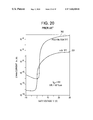
- FIG. 29 shows a schematic configuration of a liquid crystal electro-optical device of one embodiment of the present invention.
- FIG. 30 shows a schematic configuration of a reflection type liquid crystal dispersion display device of one embodiment of the present invention.
- FIG. 31 illustrates an example of the circuit configuration of a liquid crystal display device of the present invention
- FIG. 32 illustrates a layout of electrodes and the like of another embodiment of the present invention.
- FIGS. 33(A) to 33(H) are cross-sectional views to show the manufacturing process for a liquid crystal panel of one embodiment of the present invention.
- FIG. 34 shows the peripheral circuitry of a liquid crystal electro-optical device of the present invention
- FIGS. 35(A) to 35(D) are graphs showing input signal waveforms inputted to and output signal waveforms outputted from the C/TFT obtained in one embodiment of the present invention.
- FIGS. 36(A) to 36(G) are cross-sectional views to show the manufacturing process for a liquid crystal display device of one embodiment of the present invention.
- FIG. 37 illustrates a layout of electrodes and the like of another embodiment of the present invention.
- FIG. 38 illustrates a layout of electrodes and the like of still another embodiment of the present invention.
- a liquid crystal display device with the circuit configuration shown in FIG. 17 , (i.e., a buffer type circuit configuration) is used.
- FIG. 38 shows the layout of the actual electrodes and the like corresponding to the circuit configuration of FIG. 17 .
- the driving signal waveform is shown in FIG. 16 .
- the explanation of the signal waveform is also given for the case of 2 ⁇ 2 matrix configuration.
- FIG. 18(A)-18(F) The manufacturing process for forming the substrate for the liquid crystal display device used in an embodiment of the present invention is shown in FIG. 18(A)-18(F) .
- a silicon oxide film for a blocking layer 951 having a thickness of 1000 to 3000 angstroms is formed on a glass substrate 950 , using a magnetron RF (high frequency) sputtering method.
- the glass substrate 950 is made of inexpensive glass capable of withstanding heat treatment up to 700° C. e.g. of 600° C.
- the film forming, using either quartz or single-crystal silicon for a target has a speed of 30 to 100 Angstroms/minute.
- an amorphous silicon film is formed using an LPCVD (low pressure chemical vapor deposition) method, sputtering method, or a plasma CVD method.
- LPCVD low pressure chemical vapor deposition
- disilane (Si 2 H 6 ) or trisilane (Si 3 H 8 ) is supplied to the CVD apparatus at a temperature 100 to 200° C. less than the crystallization temperature (i.e., 450 to 550° C., for example at 530° C.).
- the pressure inside the reaction furnace is 30 to 300 Pa.
- the film forming speed is 50 to 250 ⁇ /minute.
- Vth threshold voltage
- boron with a concentration of 1 ⁇ 10 15 to 5 ⁇ 10 18 cm ⁇ 3 can be added using diborane. If using a sputtering method, the conditions are as follows:
- the temperature is 300° C. for example, and monosilane (SiH 4 ) or disilane (Si 2 H 6 ) is used as the reactive gas, which are input into a PCVD apparatus and 13.56 MHz high frequency electric power is applied for film forming.
- the oxygen concentration of the film formed is 5 ⁇ 10 21 cm ⁇ 3 or less. If the oxygen concentration is higher than this range, crystallization becomes difficult and the heat annealing temperature must be high or the annealing time long. On the other hand, if the concentration is too low, the current leak in the OFF state increases because of the back light. For this reason the concentration is held in the range from 4 ⁇ 10 19 to 4 ⁇ 10 21 cm ⁇ 3 .
- the silicon concentration is assumed to be 4 ⁇ 10 22 cm ⁇ 3 and hydrogen concentration is 4 ⁇ 10 20 cm ⁇ 3 , which is equal to one atomic % of the silicon concentration.
- the oxygen concentration is adjusted to 7 ⁇ 10 19 cm ⁇ 3 or less, or, preferably, 1 ⁇ 10 19 cm ⁇ 3 or less, and oxygen may be added by ion implantation to a concentration range of 5 ⁇ 10 20 to 5 ⁇ 10 21 cm ⁇ 3 , only to the channel forming regions of the TFTs which form the pixels.
- it is effective for a high frequency operation to reduce the amount of oxygen contained in the TFT provided in the peripheral circuits which no light reaches, so as to make the carrier mobility greater.
- an intermediate heat treatment is performed at 450 to 700° C. for 12 to 70 hours in an oxygen-free atmosphere, for example, in a hydrogen atmosphere at 600° C.
- an amorphous silicon oxide film is formed on the surface of the substrate, beneath the silicon film, no specific nucleus exists in this heat treatment, so the whole amorphous silicon film is uniformly heat annealed. Specifically, the amorphous structure is kept in film forming and hydrogen is merely mixed in.
- a peak is shifted from 522 cm ⁇ 1 of the single crystal silicon to a lower frequency side.
- the apparent grain diameter when calculated using the half-value width, is 50 to 500 ⁇ , like a micro crystal. Actually, many of these highly crystallized regions make up clusters. Each cluster is joined to the other by a silicon junction forming (i.e., anchoring) a semi-amorphous film.
- the film could be said to have substantially no grain boundary (GB).
- the carriers can easily travel between the clusters through the anchored areas, so that the mobility of the carriers is higher than that of the poly-crystalline silicon having clear grain boundaries (GB).
- FIG. 18(A) shows the silicon film which is photoetched using a first photomask 91 , with the NTFT region 913 (20 um in channel width) prepared at the left side of the drawing and the PTFT region 922 at the right side.
- a silicon oxide film is then formed as a gate insulation film in the thickness range of 500 to 2000 ⁇ (e.g., 1000 ⁇ ). This is prepared under the same conditions as the silicone oxide film formed as a blocking layer. A small amount of fluorine may be added to this film for fixation of the sodium ion during film forming.
- a silicon film is provided containing a 1 to 5 ⁇ 10 21 cm ⁇ 3 concentration of phosphorus. Molybdenum (Mo), tungsten (W), MoSi 2 or WSi 2 film may be optionally formed on this silicon film to form a multilayer film.
- the silicon film (or multilayer film) is patterned with a second photomask 92 to obtain the configuration shown in FIG. 18(B) .
- An NTFT gate electrode 909 and a PTFT gate electrode 921 are then formed. For example, as a gate electrode, a phosphorus-doped silicon 0.2 ⁇ m thick is formed and a molybdenum layer 0.3 ⁇ m thick is formed thereon with a channel length of 10 ⁇ m.
- a photoresist 957 is formed using a photomask 93 , and boron is added using the ion implantation method at a dosage of 1 to 5 ⁇ 10 15 cm ⁇ 2 for the PTFT source 918 and drain 920 .
- boron is added using the ion implantation method at a dosage of 1 to 5 ⁇ 10 15 cm ⁇ 2 for the PTFT source 918 and drain 920 .
- a photoresist 961 is formed using a photomask 94 .
- Phosphorous is added using the ion implantation method at a dosage of 1 to 5 ⁇ 10 15 cm ⁇ 2 for an NTFT source 910 and drain 912 .
- the TFT characteristics can be further increased by improving the mobility and decreasing the threshold voltage.
- the doping above is made through a gate insulation film 954 .
- the silicone oxide on the silicone film may be removed followed by the addition of the boron and phosphorous directly into the silicon film using the ion implantation method.
- annealing is again conducted for 10 to 50 hours at 600° C.
- the impurities of the NTFT source 910 and drain 912 , and the PTFT source 918 , and drain 920 , are activated to form P+ and N+ regions.
- the channels 919 and 911 below the gate electrodes 921 and 909 are made of a semi-amorphous semiconductor.
- this embodiment of the invention is very suitable for a liquid crystal display having a large picture element.
- the heat anneal process shown in FIG. 18(A) and FIG. 18(D) , is performed twice. However, the anneal process of FIG. 18(A) can be omitted, depending on the desired characteristics, and followed up with the heat anneal process of FIG. 18(D) , thereby shortening the manufacturing time. Also, in FIG. 18(E) , the interlayer insulation layer 965 is made of silicon oxide film using the sputtering method mentioned above.
- This silicon oxide film can, however, also be formed using the LPCVD method or photo CVD method or normal pressure CVD method.
- the thickness of the insulation layer is e.g. 0.2 to 0.6 ⁇ m.
- a window 966 for the electrodes is formed.
- a layer of aluminum is formed over the entire structure using the sputtering method, and leads 971 and 972 and contacts 967 , 968 are made using photo mask 96 .
- An organic resin film 969 for surface-flattening, e.g. a transparent polyimide resin film is formed, and electrode open-ings are provided using photomask 97 .
- Two TFTS are formed in a complementary structure in a picture element of the liquid crystal display device as shown in FIG. 18(F) .
- the output terminals of the TFTS are each connected to the (transparent) electrode of the picture element of the liquid crystal display device, forming the ITO (Indium Tin Oxide) by sputtering.
- the electrode 917 is completed by etching through the photomask 98 .
- the ITO film is formed in the range from room temperature to 150° C. and finished by annealing at 200° C. to 400° C. in oxygen or atmosphere.
- the NTFT 913 , the PTFT 922 and the transparent electrode 917 are thus prepared on a single glass substrate 950 .
- FIG. 38 illustrates the positioning of the electrodes and the like for the liquid crystal display device according to this embodiment.
- An NTFT 913 is provided at the intersection of a first signal line 905 and a third signal line 903 , and, in the same manner, an NTFT for another picture element is provided at the intersection of the first signal line 905 and a third signal line 904 .
- a PTFT is provided at the intersection of a second signal line 908 and the third signal line 903 .
- an NTFT for another picture element is provided at the intersection of another, adjacent first signal line 906 and the third signal line 903 , while in the same manner an NTFT is provided at the intersection of the first signal line 906 and the third signal line 904 .
- the NTFT 913 is connected to the first signal line 905 through a contact on the input terminal on the drain 910 , and the gate 909 is connected to a signal line 903 which is formed of multilayer wiring.
- the output terminal of the source 912 is connected to a picture element electrode 917 through a contact.
- the PTFT 922 is connected to the second signal line 908 through a contact on the input terminal on the drain 920 , wherein the gate 921 is connected to the signal line 903 , and the output terminal of the source 918 is connected to the picture element electrode 917 through a contact in the same way as in the NTFT.
- An adjacent C/TFT is connected to signal line 903 , and the PTFT 922 of the C/TFT is connected to a second signal line 907 . Also, the NTFT 913 of the adjacent C/TFT is connected to the first signal line 906 .
- One pixel comprising a picture element 923 , formed from a transparent conducting film and a C/TFT, is interposed between this pair of signal lines 905 and 908 .
- the 2 ⁇ 2 matrix can be expanded to form a large picture element liquid crystal display device of 640 ⁇ 480 or 1280 ⁇ 960 matrixes.
- a special feature of the device of the present invention is that the picture element electrode 917 is set at three values of the liquid crystal potential V LC by providing a complementary configuration of two TFTs for one picture element.
- an ITO film (Indium Tin Oxide) is formed by sputtering on a substrate which is formed by laminating a silicon oxide film to a thickness of 2000 ⁇ on glass plate by the sputtering process.
- This ITO film is formed in the range from room temperature to 150° C. and finished by annealing at 200° C. to 400° C. in oxygen or atmosphere.
- a polyimide precursor member is printed on the above-mentioned substrate using the offset method and fired for one hour at 350° C. in an oxygen-free atmosphere (for example, in a nitrogen atmosphere).
- the polyimide surface is then reformed using a commonly known rubbing method, so that a means for orienting the liquid crystal molecules in a uniform direction in at least the initial stage is provided, whereby the second substrate is completed.
- liquid crystal composition having ferroelectricity
- the assembly is sealed around the periphery using an epoxy-type adhesive.
- a drive IC of a TAB form is connected to a lead on the substrate and a polarizing plate is affixed to the outside to obtain a light-transmission type of liquid crystal display device.
- FIG. 14 shows the display for the A, E, and C picture elements when the drive waveform shown in FIG. 16 is applied.
- darkness is expressed by a dot.
- a clear gradated display is obtained, as shown in FIG. 14 .
- a first substrate and a second substrate are obtained using the same process as for the Embodiment 1. However, no polyimide film for alignment is formed on the second substrate. Since this device is made for use in a video camera viewfinder, the pitch of the picture element is 60 ⁇ m, and a matrix 200 high ⁇ 300 wide is formed.
- a nematic liquid crystal composition is dispersed throughout an acrylic organic resin to form a dispersed-type liquid crystal display device.
- 62 wt % of the nematic liquid crystals is dispersed throughout an acrylic resin denatured with an ultraviolet-curable epoxy.
- This material is interposed between the first and second substrates, and is then cured by the application of a light beam from a UV light source with a 1000 mW output for 20 sec.
- This display device is time-shared into 16 separate time periods to provide a gradated display, and each color has 16 gradations, to give a liquid crystal display device which can display a total of 4096 colors.
- the drive wave form at that time is shown in FIG. 19 .
- a plurality of write-in entries is provided in conventional gradated display methods.
- 16 frames are utilized to provide a method for presenting a gradated display by a combination of their ON/OFF states. If, in a total 16 frames, eight frames are ON and the remaining eight frames are OFF, a gradated display results at a 50% transmission, which is the average transmittance in this case. If, however, four frames are ON and the remaining 12 frames are OFF, the average transmittance becomes 25% and a gradated display occurs at this transmission.
- a gradated display becomes possible preventing the actual frame frequency from decreasing. Therefore, the frequency is never lower than a visually confirmed frequency, so that a drop in display quality does not occur, and a high quality picture can be provided.
- the liquid crystal electro-optical device utilized in a third embodiment of the present invention has the circuit configuration shown in FIG. 10 , namely, the circuit configuration of inverter type.
- FIG. 12 shows the layout of the actual electrodes and the like corresponding to the circuit configuration of FIG. 10 . In order to simplify the explanation, the parts corresponding to a 2 ⁇ 2 matrix only are described. Also, the actual driving signal waveform is shown in FIG. 9 .
- FIGS. 13(A) to (F) The process for forming a substrate for the liquid crystal electro-optical device utilized in this embodiment is shown in FIGS. 13(A) to (F).
- the substrate shown in FIG. 13(F) is formed in the same manner as in Embodiment 1.
- the substrate has the same structure as that in Embodiment 1 except that the location of a PTFT and an NTFT thereof is opposite to that of Embodiment 1, as shown in FIGS. 10 and 13 .
- a light-transmission type liquid crystal electro-optical device is completed as in Embodiment 1.
- a first substrate and a second substrate are obtained using the same process as described with respect to the third embodiment.
- an orientation film made of polyimide is not formed on the second substrate.
- a liquid crystal electro-optical device for use in a video camera viewfinder is formed at a pitch of a picture element of 60 ⁇ m, and a matrix 200 high ⁇ 300 wide in the same way as in Embodiment 2.
- a gradated display becomes possible, preventing the actual frame frequency from decreasing. Therefore, the frequency never becomes lower than a visually confirmed frequency, so that a drop in display quality does not occur, and a high quality picture can be provided.
- each color is displayed with 16 gradations, so that a display with 4096 colors is possible in total.
- FIG. 5 shows the layout of the actual electrodes and the like corresponding to the circuit configuration of FIG. 3 .
- FIGS. 6(A)-6(D) The manufacturing process for the liquid crystal display device used in this embodiment is shown in FIGS. 6(A)-6(D) .
- a silicon oxide film for a blocking layer 51 having a thickness of 1000 to 3000 angstroms is formed on a glass substrate 50 , using a magnetron RF (high frequency) sputtering method.
- the glass substrate 50 utilized is the one which is not expensive unlike quartz glass and is resistant to heat treatment up to 700° C. e.g. of 600° C.
- the conditions for the process are as follows:
- the film formation using either quartz or single-crystal silicon for a target, has a speed of 30 to 100 ⁇ /min.
- boron may be added at a concentration of 1 ⁇ 10 15 to 1 ⁇ 10 18 cm ⁇ 3 by the use of diborane during the film formation, in order to control the threshold voltage (Vth) of the NTFT.
- the silicon film in an amorphous state is heat-annealed at an intermediate temperature of 450 to 700° C. for 12 to 70 hours under a non-oxide atmosphere. Then, an NTFT region 13 is obtained from the silicon film by the use of a first photomask 1 .
- a silicon oxide film is then formed as a gate insulating film 54 in the thickness range of 500 to 2000 ⁇ (e.g., 1000 ⁇ ). This is prepared under the same conditions as the silicone oxide film formed as a blocking layer. A small amount of fluorine may be added to the film for fixation of the sodium ion during the film formation.
- a silicon film containing a 1 to 5 ⁇ 10 21 cm ⁇ 3 concentration of phosphorus, or a multilayered film comprising the silicon film laminated thereon with molybdenum (Mo), tungsten (W), MoSi 2 or WSi 2 film is formed.
- the film is then patterned with a second photomask 2 to obtain the configuration shown in FIG. 6(B) .
- Phosphorus is added by ion implantation method at a dosage of 1 to 5 ⁇ 10 15 cm ⁇ 2 for a NTFT source 20 and drain 18 , using the gate electrode 9 as a mask.
- the TFT characteristics can be further increased by improving the mobility and decreasing the threshold voltage.
- the above-described process is carried out through the gate insulating film 54 .
- annealing is again conducted for 10 to 50 hours at 600° C.
- the impurities are activated whereby the source 20 and drain 18 of the NTFT are made N + regions.
- a channel forming region 21 of semi-amorphous semiconductor is formed below the gate electrode 9 .
- this embodiment of the invention is very suitable for a liquid crystal display having a large number of pixels.
- the heat anneal process is carried out twice as shown in FIGS. 6(A) and (C). However, the anneal process of FIG. 6(A) may be omitted, depending on the desired characteristics, and followed up with the heat anneal process of FIG. 6(C) , thereby shortening the manufacturing time. Also, in FIG. 6(D) , the interlayer insulating layer 65 is made of silicon oxide film using the sputtering method mentioned above.
- the silicon oxide film can, however, also be formed using the LPCVD method or photo CVD method or normal pressure CVD method.
- the thickness of the film is e.g. 0.2 to 0.6 ⁇ m.
- an opening 66 for the electrodes is formed.
- a layer of aluminum is formed on the entire surface by sputtering, and leads 71 and 72 and contacts 67 , 68 are formed by using photo mask 4 .
- An organic resin film 69 for surface-flattening, e.g. a transparent polyimide resin film is formed, and openings for electrodes are provided using a photomask 5 .
- the TFT is thus formed as shown in FIG. 6(F) , and further an ITO (Indium Tin Oxide) film is formed by sputtering so that the output terminal of the TFT is connected to a transparent electrode of the picture element of the liquid crystal display device by the ITO.
- ITO Indium Tin Oxide
- the electrode is completed by etching the ITO film through a photomask 6 , whereby a pixel electrode 17 and a contact 73 of the pixel electrode with the drain electrode are completed.
- This ITO film is formed in the range from room temperature to 150° C. and annealed at 200° C. to 400° C. in oxygen or atmosphere.
- the NTFT 13 and the transparent pixel electrode 17 are thus prepared on an identical glass substrate 50 .
- the electrical characteristics of the TFT formed are as follows:
- a second substrate is manufactured in the same manner as the second substrate of the first embodiment.
- the liquid crystal composition exhibiting ferroelectricity is interposed between the first and second substrates, and the assembly is sealed around the periphery using an epoxy-type adhesive.
- a drive IC of a TAB form is connected to a lead on the substrate and a polarizing plate is affixed to the outside to obtain a light-transmission type of liquid crystal display device.
- FIG. 7 shows the display for the A, F, and I picture elements when the drive waveform shown in FIG. 1 is applied.
- FIG. 7 additionally shows that a clear gradated display is obtained.
- a first substrate and a second substrate are obtained using the same process as for the fifth embodiment.
- an orientation film made of polyimide is not formed on the second substrate.
- a liquid crystal electro-optical device for use in a video camera viewfinder is formed at a pitch of a picture element of 60 ⁇ m and a matrix 200 high ⁇ 300 wide in the same way as in the second embodiment of the present invention.
- each color is displayed with 16 gradations, so that a display with 4096 colors is possible in total.
- a gradated display becomes possible, thereby preventing the actual frame frequency from decreasing. Therefore, the frequency never becomes lower than a visually confirmed frequency, so that a drop in display quality does not occur, and a high quality picture can be provided.
- the quality of gradated displays can be improved over conventional displays by performing the above-mentioned conventional method for gradated display together with the method for gradated display in accordance with the present invention.
- the method of the present invention is to control the average voltage applied to a liquid crystal pixel, where complete response of liquid crystal is not required.
- the present invention provides a method for controlling liquid crystal which responds incompletely.
- N-channel field effect transistors are utilized in this embodiment, P-channel field effect transistors may also be utilized.
- a liquid crystal electro-optical device (image display device) with the circuit configuration shown in FIG. 21 is utilized as a television to be placed on a wall, for example.
- the TFTs utilized therein are made of polycrystal silicon subjected to laser annealing and are of stagger type.
- a gate electrode 700 a source 701 , a drain 702 , a NMOSTFT 703 , and a pixel electrode 704 are shown. Also illustrated in FIG. 21 is a lead contact 705 and a pixel contact 706 .
- the layout of the actual electrodes and the like corresponding to the circuit configuration in FIG. 21 is shown in FIG. 37 . To simplify the explanation, the parts corresponding to a 2 ⁇ 2 (or less) matrix only are described. Also, the reference numerals are made so as to correspond to those in FIG. 21 . Further, the actual driving signal waveform is shown in FIG. 1 . For simplicity, the explanation of the signal waveform is also given for the case of 4 ⁇ 4 matrix configuration.
- FIGS. 22(A)-22(I) The manufacturing process for the liquid crystal display device used in this embodiment is shown in FIGS. 22(A)-22(I) .
- a silicon oxide film for a blocking layer 801 having a thickness of 1000 to 3000 angstroms is formed on a glass substrate 800 , using a magnetron RF (high frequency) sputtering method.
- the glass substrate 800 utilized is the one which is not expensive unlike quartz glass and is resistant to heat treatment up to 700° C. e.g. of 600° C.
- the conditions for the process are as follows:
- the film formation using either quartz or single-crystal silicon for a target, has a speed of 30 to 100 ⁇ /min.
- a silicon film in an amorphous state is formed on the silicon oxide film.
- the film formation temperature is from 250° C. to 350° C. (e.g. 320° C. in this embodiment), and monosilane (SiH 4 ) is utilized.
- monosilane SiH 4
- disilane Si 2 H 6
- trisilane Si 3 H 8
- the gas is inputted to a PCVD apparatus, maintained at a pressure of 3 Pa and a high frequency electric power, is applied thereto at a frequency of 13.56 MHz, whereby the silicon film is deposited.
- a high frequency electric power of 0.02 to 0.10 W/cm 2 is appropriate in this case, and in this embodiment a high frequency electric power of 0.055 W/cm 2 is applied.
- the flux of the monosilane is at 20SCCM and the film formation rate under this condition is about 120 ⁇ /min.
- Boron may be added at a concentration of 1 ⁇ 10 15 to 1 ⁇ 10 18 cm ⁇ 3 by using diborane during the film formation, in order to control the threshold voltage (Vth) of the NTFT.
- this plasma CVD method but also sputtering method and low pressure CVD method can be utilized for forming the silicon film to be a channel region in a TFT.
- the conditions are as follows:
- disilane (Si 2 H 6 ) or trisilane (Si 3 H 8 ) is supplied to the CVD apparatus at a temperature 100 to 200° C. less than the crystallization temperature (i.e., 450 to 550° C., for example at 530° C.).
- the pressure inside the reaction furnace is 30 to 300 Pa.
- the film forming speed is 50 to 250 ⁇ /minute.
- the oxygen concentration is 5 ⁇ 10 21 cm ⁇ 3 or less.
- the oxygen concentration is 7 ⁇ 10 19 cm ⁇ 3 or less, preferably 1 ⁇ 10 19 cm ⁇ 3 or less.
- the concentration is too low, the current leak in the OFF state increases because of the back light. If the oxygen concentration is too high, crystallization becomes difficult and the laser annealing temperature must be increased or the annealing time lengthened.
- the silicon concentration is assumed to be 4 ⁇ 10 22 cm ⁇ 3 and the hydrogen concentration is 4 ⁇ 10 20 cm ⁇ 3 which is equal to one atomic % of the silicon concentration.
- the oxygen concentration is adjusted to 7 ⁇ 10 19 cm ⁇ 3 or less, or, preferably, 1 ⁇ 10 19 m ⁇ 3 or less, and oxygen may be added by ion implantation to a concentration range of 5 ⁇ 10 20 to 5 ⁇ 10 21 cm ⁇ 3 , only to the channel forming regions of the TFTs which form the pixels.
- the silicon film 802 in an amorphous state is formed to be 500 to 5000 ⁇ in thickness, (e.g., 1000 ⁇ in this embodiment).
- photoresist 803 is formed in a pattern having openings therein on source and drain regions as shown in FIG. 22(B) by the use of a mask 1 .
- a silicon film 804 to be an n-type activation layer is formed by plasma CVD.
- the film formation temperature is 250° C. to 350° C. (specifically 320° C. in this embodiment).
- Monosilane (SiH 4 ) and phosphine (PH 3 ) of monosilane base at a concentration of 3% are utilized. They are introduced into a PCVD apparatus maintained at a pressure of 5 Pa and an electric power at a high frequency of 13.56 MHz is inputted thereto, whereby the silicon film 804 is deposited.
- the high frequency electric power of 0.05 to 0.20 W/cm 2 is appropriate in this case. In this embodiment an electric power of 0.120 W/cm 2 is inputted.
- the n-type silicon film formed by the above-described method has a specific electric conductivity of about 2 ⁇ 10 1 [ ⁇ cm ⁇ 1 ]. The thickness thereof is 50 ⁇ .
- source and drain regions 805 and 806 are formed by a lift-off method. After that, an island region 807 for an N-channel thin film transistor is formed using a mask 82 .
- laser annealing to the source, drain, channel regions and laser doping to the activation layer are carried out simultaneously by the use of XeCl excimer laser.
- the threshold energy of this laser at this moment is 130 mJ/cm 2 .
- the energy of 220 mJ/cm 2 is necessary.
- a laser at 150 mJ/cm 2 is irradiated to discharge hydrogen and then a laser at 230 mJ/cm 2 is irradiated to crystallize the film.
- the film can be said to have substantially no grain boundary (GB).
- the carriers can easily travel between the clusters through the anchored areas, so the mobility of the carriers is higher than that of the poly-crystalline silicon, having clear grain boundaries (GB).
- the electron mobility (ue) obtained is 15 to 300 cm 2 /Vsec.
- a silicon oxide film 808 is then formed as a gate insulating film in the thickness range of 500 to 2000 ⁇ (e.g., 1000 ⁇ ). This is prepared under the same conditions as the silicon oxide film formed as a blocking layer. A small amount of fluorine may be added to this film for fixation of the sodium ion during film formation.
- a silicon film containing phosphorus at a concentration of 1 to 5 ⁇ 10 21 cm ⁇ 3 , or a multilayered film comprising the silicon film laminated thereon with molybdenum (Mo), tungsten (W), MoSi 2 or WSi 2 film is formed.
- This film is patterned with a third photomask 83 to obtain the configuration shown in FIG. 22(E) .
- a gate electrode 809 is then formed. For example, as a gate electrode, a phosphorus-doped silicon 0.2 ⁇ m thick is formed and a molybdenum layer 0.3 ⁇ m thick is formed thereon with a channel length of 7 ⁇ m.
- the TFT characteristics can be further increased by improving the mobility and decreasing the threshold voltage.
- this embodiment of the invention is very suitable for a liquid crystal display having a large number of picture elements.
- a silicon oxide film is formed as an interlayer insulator 810 by a sputtering method.
- a LPCVD method, a photo CVD method, and a normal pressure CVD method may be utilized for the formation of the silicon oxide film.
- the thickness of the layer is 0.2 to 0.6 ⁇ m, for example.
- an opening 811 for electrode is formed using a forth photomask 84 .
- an aluminum film having a thickness of 0.3 ⁇ m is formed by sputtering method, and then a lead 812 and a contact 813 are formed using a photomask ( 85 ).
- An organic resin for surface-flattering 814 e.g. a transparent polyimide resin
- an opening for an electrode is again formed using a sixth photomask 86 .
- ITO Indium Tin Oxide
- This ITO film is formed at room temperature to 150° C. and annealed at 200° C. to 400° C. in an oxygen or an atmosphere.
- the electrical characteristics of the formed TFT are as follows:
- the first substrate for a liquid crystal electro-optical device is completed.
- FIGS. 23(A)-23(E) The method for forming the second substrate is shown in FIGS. 23(A)-23(E) .
- a polyimide resin film, made of polyimide mixed with black pigment, having a thickness of 1 ⁇ m is formed on a glass substrate 500 by a spin coat method and is patterned into black stripes 501 by the use of a first photomask 411 .
- a film of polyimide resin mixed with red pigment having a thickness of 1 ⁇ m is formed by spin coat method and is subsequently patterned into red color filters 502 by the use of a second photomask 412 .
- green color filters 503 are formed by the use of a third photomask 413 , and blue color filters 504 by the use of a fourth photomask 414 .
- the filters are baked at 350° C. for 60 min. in an nitrogen atmosphere.
- a transparent polyimide layer is formed as a leveling layer 505 by spin coat method.
- an ITO film of 0.1 ⁇ m thickness is formed by sputtering and is patterned into a common electrode 506 by the use of a fifth photomask 415 .
- This ITO film is formed at room temperature to 150° C. and annealed at 200 to 300° C. in an oxygen or an atmosphere. Thus, the second substrate is completed.
- a polyimide precursor material is printed on the above-described substrates by an off-set method and baked at 350° C. for 1 hour in an non-oxide atmosphere, (e.g., in nitrogen). Then the surface of the polyimide is subjected to a known rubbing method, so as to provide a means for orienting liquid crystal molecules in a fixed direction in at least an initial stage.
- a nematic liquid crystal composition is interposed between the first and second substrates and the periphery of the substrates, is sealed with an epoxy adhesive.
- An drive IC in TAB form and a PCB comprising a common signal wiring and an electric potential wiring are connected to the lead on the substrate, and a polarizing plate is affixed to the outside, whereby a light-transmission type liquid crystal electro-optical device is obtained.
- FIG. 24 shows the schematic configuration of the electro-optical device obtained in accordance with this embodiment.
- the liquid crystal panel 1000 obtained by the above steps is combined with a back light device 1001 comprising three cool cathode tubes.
- a tuner 1002 for receiving TV electric waves is connected thereto, to complete an electro-optical device. Since the electro-optical device obtained has a flat form compared with the conventional CRT type electro-optical device, it is possible to hang it on the wall and the like.
- the peripheral circuitry comprises a driver circuit 1103 connected to information signal side wires 1101 and 1102 which are connected to the matrix circuit of the liquid crystal electro-optical device.
- the driver circuit 1103 is divided into two drive frequency systems. One of them is a data latch circuit system 1104 having a drive method same as the conventional method, where the main composition is a basic clock CLK 1 1106 for transferring data 1105 by turns and 1-12 bits parallel processing.
- the other is the system composed in accordance with the present invention. It is composed of a flip flop circuit 1108 , a counter 1109 and a clock CLK 2 , 1107 for the independent frequency from the data transfer frequency. Pulses are formed by the counter 1109 so as to correspond to the gradated display data transmitted from the data latch system 1104 .
- the present invention is directed to this type of system. That is, by utilizing two kinds of drive frequency, a clear digital gradated display can be obtained without reducing frame numbers for rewriting a picture. Accordingly, occurrence of flicker and the like due to the reduction of the frame number can be avoided.
- a driver circuit 1112 connected to scanning signal lines 1110 and 1111 , the electric potential transmitted from a voltage level 1113 is controlled by a flip flop circuit 1115 of a clock CLK 1114 to supply address signals.
- a gradated display of 16 gradations is its limit due to the variation of the TFT characteristics.
- a gradated display of 42 gradations is possible.
- a colorful, fine display of 74,088 colors is possible.
- the eighth embodiment of the present invention describes the manufacture of a video camera viewfinder utilizing a liquid crystal electro-optical device of 1 inch diagonal.
- a device utilizing amorphous TFTs in a 387 ⁇ 128 matrix by low temperature processing is formed for a viewfinder.
- the manufacturing method of the liquid crystal display device utilized in this embodiment is explained below with reference to FIG. 26 .
- a silicon oxide film of 1000 to 3000 ⁇ thickness is formed as a blocking layer 1201 on inexpensive glass 1200 such as soda-lime glass by magnetron RF (high frequency) sputtering method.
- the process conditions are as follows:
- Quartz or single-crystal silicon is utilized as a target, and the film formation speed is 30 to 100 ⁇ /min.
- a silicon film containing a 1 to 5 ⁇ 10 21 cm ⁇ 3 concentration of phosphorus, or a multilayered film comprising the silicon film laminated thereon with molybdenum (Mo), tungsten (W), MoSi 2 or WSi 2 film is formed, which is then patterned with a first photomask 21 to form a gate electrode 1202 as in FIG. 26(A) .
- the channel length is 10 um and as a gate electrode a phosphorus doped silicon film of 0.2 ⁇ m thickness is formed and a molybdenum film of 0.3 ⁇ m thickness is formed further thereon.
- the TFT characteristics can be further increased by improving mobility and decreasing the threshold voltage.
- a silicon oxide film is then formed as a gate insulating film 1203 in the thickness range of 500 to 2000 ⁇ (e.g., 1000 ⁇ ). This is prepared under the same conditions as the silicon oxide film formed as a blocking layer. A small amount of fluorine may be added to this film for fixation of the sodium ions during the film formation.
- An amorphous silicon film is then formed on this structure by plasma CVD method.
- the temperature is maintained at e.g. 300° C. and monosilane (SiH 4 ) or disilane (Si 2 H 6 ) is utilized.
- the gas is introduced into a PCVD apparatus and a high frequency electric power of 13.56 MHz is input thereto, whereby the film is formed.
- the oxygen concentration is 5 ⁇ 10 21 cm ⁇ 3 or less. If the oxygen concentration is higher than this range, the mobility is decreased. If the concentration is too low, the current leak in the OFF state increases because of the back light. For this reason, the concentration is held in the range from 4 ⁇ 10 19 to 4 ⁇ 10 21 cm ⁇ 3 . Silicon concentration is assumed to be 4 ⁇ 10 22 cm ⁇ 3 . Hydrogen concentration is 4 ⁇ 10 2 cm 3 which is equal to one atomic % of the silicon concentration. In accordance with the above method, a silicon film in an amorphous state is formed to be 500 to 5000 ⁇ thick (e.g., 1500 ⁇ ).
- a resist film 1204 for forming a contact region by lift-off method is formed utilizing a second photomask 22 , and on the top surface a silicon film 1205 to be an n-type activation layer is formed by plasma CVD.
- the film formation temperature is in the range from 250° C. to 350° C. (at 320° C. in the present embodiment)
- Monosilane and monosilane-based phosphine (PH 3 ) at a concentration of 1% and hydrogen (H 2 ) are introduced at a ratio of 5:3:20 into a PCVD apparatus at a pressure of 5 Pa and a high frequency electric field at 13.56 MHz is applied to form the silicon film.
- a high frequency electric power of 0.05 to 0.20 W/cm 2 is appropriate, and an electric power of 0.120 W/cm 2 is utilized in this embodiment.
- the formed silicon film 1205 to be an n-type activation layer has a specific electric conductivity of about 2 ⁇ 10 ⁇ 1 ncm ⁇ 1 .
- the film thickness thereof is 50 ⁇ .
- aluminum film 1206 of 3000 ⁇ thickness is formed for a lead and a contact electrode by sputtering. Unnecessary portions of the aluminum film are removed by lift-off method to form a source region 1207 and a drain region 1208 .
- an organic resin 1210 for surface flattering e.g., a transparent polyimide resin
- an opening for electrode is again formed by the use of a photomask 24 .
- an ITO (Indium Tin Oxide) film is formed by sputtering method.
- the ITO film is subjected to etching by using a photomask 25 to form an electrode 1211 .
- the ITO film is formed at room temperature to 150° C. and annealed at 200° C. to 400° C. in an oxygen or an atmosphere.
- an NTFT 1209 and an electrode 1211 made of a transparent conductive film are formed on an identical glass substrate 1200 .
- the electrical characteristics of the thus obtained TFT are as follows:
- color filters and a transparent conductive film of ITO are formed to a thickness of 1000 ⁇ on an insulating substrate to obtain a second substrate.
- a polyimide precursor material is printed by off-set printing and baked at 350° C. for 1 hour in an non-oxidation atmosphere (e.g., in nitrogen).
- the surfaces of the polyimide are then subjected to a known rubbing treatment to provide a means for orienting liquid crystal molecules in a fixed direction in at least an initial stage.
- a known rubbing treatment to provide a means for orienting liquid crystal molecules in a fixed direction in at least an initial stage.
- a nematic liquid crystal composition is interposed between the first and the second substrates, and the periphery thereof is sealed with an epoxy adhesive. Since the pitch of the leads on the substrate is so fine as 46 ⁇ m, the connection is carried out by the use of COG method.
- leads are connected to gold bumps provided on an IC chip by means of a silver paradium resin of epoxy system. Then an epoxy transformed acrylic resin is filled in the space between the substrate and the IC chip for the purpose of fixing and enclosing the IC chip and the substrates. Then a polarizing plate is affixed to the outside thereof, whereby a light-transmission type liquid crystal display device is obtained.
- the variation of the amorphous TFT characteristic is about ⁇ 10%, so that a gradated display of 8 gradations is its limit.
- the method is not affected by the variation of TFT characteristic so much, so that a gradated display of 13 gradations or more is possible.
- a color display In the case of a color display, a colorful, fine display of 2027 colors is possible.
- the ninth embodiment of the present invention the manufacture of a projection type image display device as shown in FIG. 27 is described.
- an image projecting part for a projection type image display device is assembled using three liquid crystal electro-optical devices 1300 . Each of them has a 640 ⁇ 480 dot matrix, and 307,200 pixels are formed within the size of 4 inch diagonal. The size of one pixel is 127 ⁇ m square.
- the projection type image display device is composed of three liquid crystal electro-optical devices 1300 for three primary colors of light (i.e., red, green, and blue respectively), a red color filter 1301 , a green color filter 1302 , a blue color filter 1303 , reflection boards 1304 , a metal halide light source 1307 of 150 W, and an optical system for focus 1308 .
- the substrate of the liquid crystal electro-optical device utilized for an electro-optical device of this embodiment has an NMOS configuration and a matrix circuitry.
- a device comprising high mobility TFTs formed by low temperature process is utilized to compose the projection type liquid crystal electro-optical device.
- a silicon oxide film of 1000 to 3000 ⁇ thickness is formed as a blocking layer 1401 on glass 1400 by magnetron RF (high frequency) sputtering as shown in FIG. 28(A) .
- the glass is the one which is not expensive unlike quartz glass and the like, and is resistant to thermal treatment at a temperature not higher than 700° C. (e.g., about 600° C.).
- the process conditions of the film formation are the same as those for the silicon oxide film as a blocking layer in the first embodiment of the invention.
- a silicon film in an amorphous state is formed to be 500 to 5000 ⁇ thick, e.g. 1500 ⁇ thick, in the same manner as the case of the silicon film in an amorphous state in the first embodiment of the invention.
- the silicon film in an amorphous state is then annealed at an intermediate temperature of 450° C. to 700° C. for 12 to 70 hours in a non-oxide atmosphere.
- the silicon film is subjected to photo etching by the use of a first photomask 31 to form a region 1402 for TFT (having a channel width of 20 ⁇ m), as shown in FIG. 28(A) .
- a silicon oxide film of 500 to 2000 ⁇ in thickness (e.g., 1000 ⁇ ) is formed as a gate insulating film 1403 .
- the formation conditions are the same as those for the silicon oxide film as a blocking layer.
- a small amount of fluorine may be added during the film formation for fixation of sodium ions.
- a silicon film containing a 1 to 5 ⁇ 10 21 cm ⁇ 3 concentration of phosphorus, or a multilayered film comprising the silicon film laminated thereon with molybdenum (Mo), tungsten (W), MoSi 2 or WSi 2 film is formed, which is subsequently patterned with a second photomask 32 to form a gate electrode 1404 as in FIG. 28(B) .
- a channel length is made 10 ⁇ m, and as a gate electrode the phosphorus doped silicon of 0.2 ⁇ m thickness is formed and further a molybdenum film of 0.3 ⁇ m thickness is laminated thereon.
- phosphorus is added by ion implantation method at a dosage of 1 to 5 ⁇ 10 15 cm ⁇ 2 to form a source 1405 and a drain 1406 .
- the TFT characteristics can be further increased by improving the mobility and decreasing the threshold voltage.
- heat annealing is again carried out at 600° C. for 10 to 50 hours.
- Impurities in the source 1405 and the drain 1406 are activated to make the source and drain N + regions.
- a channel forming region 1407 of semi-amorphous semiconductor is formed below the gate electrode 1404 .
- this embodiment of the invention is very suitable for a liquid crystal display having a large number of pixels.
- the heat annealing process is carried out twice as shown in FIGS. 28(A) and (C).
- the anneal process of FIG. 28(A) may be omitted, depending on the desired characteristics, and followed up with the heat anneal process of FIG. 28(C) , shortening the manufacturing time.
- an interlayer insulating layer 1408 is made of silicon oxide film using the sputtering method mentioned above.
- This silicon oxide film can, however, be formed using a LPCVD method, a photo CVD method or a normal pressure CVD method.
- the thickness of the insulating layer is e.g. 0.2 to 0.6 ⁇ m.
- an opening 1409 for the electrodes is formed.
- a layer of aluminum is formed over the entire structure using the sputtering method, and a lead 1410 and a contact 1411 are formed using photomask 34 .
- An organic resin film 1412 for surface-flattering (e.g., a transparent polyimide resin film) is formed, and an opening for an electrode is formed using photomask 35 .
- an ITO (Indium Tin Oxide) film is formed by sputtering.
- the ITO film is etched by the use of a photomask 36 to form an electrode 1413 .
- the ITO film is formed at room temperature to 150° C. and annealed at 200 to 400° C. in an oxygen or an atmosphere.
- the NTFT 1402 and the electrode 1413 of a transparent conductive film are formed on an identical glass substrate 1400 .
- the electrical characteristics of the obtained TFT are as follows:
- FIG. 29 A schematic view of the structure is shown in FIG. 29 .
- a mixture of loum thickness is formed by die-cast method, the mixture comprising fumaric acid polymeric resin and nematic liquid crystal both dissolved at a ratio of 65:35 in a common solvent, xylene.
- the above structure is heated at 120° C. for 180 min. in a nitrogen atmosphere to remove the solvent, whereby a liquid crystal dispersion layer 1501 is formed. It is found that tact-time could be shortened by making the pressure a bit lower than the atmospheric pressure at the moment.
- an ITO film is formed by sputtering to obtain an opposed electrode 1502 .
- This ITO film is formed at room temperature to 150° C.
- a transparent silicon resin is then applied to be 30 um thick by printing method and is baked at 100° C. for 30 min. to obtain a liquid crystal electro-optical device.
- the configuration and the function of the driver IC utilized in this embodiment is the same as that in the seventh embodiment of the present invention.
- the method is not affected by the variation in TFT characteristics much, so that a gradated display of 86 gradations is possible.
- a color display a colorful, fine display having 262,144 colors can be obtained.
- a conventional television set utilizing a liquid crystal display having 16 gradations is not suitable for displaying a natural landscape.
- a hollow (uneven) surface of a ‘lock’ of one color should be displayed by subtly different colors in order to express a variety of shades of the hollow (uneven) surface in sunshine.
- the gradated display in accordance with the present invention, makes it possible to project a picture (e.g., a ‘lock’ of one color) with variations of fine tone.
- This liquid crystal electro-optical device is applicable not only to a front type projection TV as shown in FIG. 27 but also a rear type projection TV.
- the tenth embodiment of the present invention shows the manufacture of an electro-optical device for a portable computer utilizing a liquid crystal dispersion type display device of reflection type as shown in FIG. 30 .
- the first substrate utilized in this embodiment is formed by the same steps as in the seventh embodiment of the invention.
- an ITO film is formed by sputtering to obtain an opposed electrode 1502 .
- This ITO film is formed at room temperature to 150° C.
- a silicon resin of white color of 55 um thickness is applied on the rear surface by printing method and baked at 100° C. for 90 minutes to obtain a liquid crystal electro-optical device.
- the eleventh embodiment of the present invention shows the manufacture of a television set to be hanged on the wall utilizing a liquid crystal display device having the circuit configuration shown in FIG. 31 .
- TFTs utilized therein are made of polycrystalline silicon subjected to laser annealing and in stagger type.
- FIG. 32 shows the layout of the actual electrodes and the like corresponding to the circuit configuration in FIG. 31 .
- the parts corresponding to a 2 ⁇ 2 (or less) matrix only are shown therein.
- the actual driving signal waveform is shown in FIG. 16 .
- the explanation of the signal waveform is also given for the case of 2 ⁇ 2 matrix configuration.
- a silicon oxide film for a blocking layer 651 having a thickness of 1000 to 3000 ⁇ is formed on a glass substrate 650 , using a magnetron RF (high frequency) sputtering method.
- the glass substrate 650 is made of inexpensive materials glass capable of withstanding heat treatment up to 700° C., e.g. about 600° C.
- a silicon film 652 in an amorphous state is formed to be 500 to 5000 ⁇ thick, e.g. 1000 ⁇ thick, in the same manner as that for the silicon film in an amorphous state in described with respect to the seventh embodiment.
- a photoresist pattern 653 with source and drain regions opened is formed using a mask P 1 .
- a silicon film to be an n-type activation layer is formed thereon by plasma CVD method.
- the film formation temperature is maintained at 250° C. to 350° C., specifically 320° C. in this embodiment.
- Monosilane (SiH 4 ) and monosilane-based phosphine (PH 3 ) at a concentration of 3% are introduced into a PCVD apparatus at a pressure of 5 Pa and a high frequency electric power at 13.56 MHz is inputted thereto, to thereby form the silicon film.
- a high frequency electric power of 0.05 to 0.20 W/cm 2 is appropriate, and a high frequency electric power of 0.120 W/cm 2 is inputted in this embodiment.
- the specific electric conductivity of the n-type silicon film thus obtained is about 2 ⁇ 10 ⁇ 1 ⁇ cm ⁇ 1 .
- the film thickness is 50 ⁇ .
- a photoresist pattern 654 with source and drain regions opened is formed using a mask P 2 , as shown in FIG. 33(C) .
- a silicon film to be a p-type activation layer is formed thereon by plasma CVD method.
- the film formation temperature is maintained at 250° C. to 350° C., specifically 320° C. in this embodiment.
- Monosilane (SiH 4 ) and monosilane-based diborane (B 2 H 6 ) at a concentration of 2% are introduced into a PCVD apparatus at a pressure of 4 Pa and a high frequency electric power at 13.56 MHz is inputted to thereby form the silicon film.
- a high frequency electric power of 0.05 to 0.20 W/cm 2 is appropriate, and a high frequency electric power of 0.080 W/cm 2 is inputted in this embodiment.
- the specific electric conductivity of the p-type silicon film obtained is about 1 ⁇ 10 ⁇ 1 ⁇ cm ⁇ 1 .
- the film thickness is 50 ⁇ .
- source and drain regions 655 , 656 and 657 , 658 are formed by lift-off method. After that, an island region 663 for an N-channel type thin film transistor and an island region 664 for a P-channel type thin film transistor are formed using a mask P 3 662 .
- a silicon oxide film of 500 to 2000 ⁇ thickness, e.g. 1000 ⁇ thickness, is then formed as a gate insulating film. This is prepared under the same conditions as the silicon oxide film formed as a blocking layer. A small amount of fluorine may be added to this film for fixation of the sodium ions during film formation.
- a silicon film containing phosphorus at 1 to 5 ⁇ 10 21 cm ⁇ 3 concentration, or a multilayered film comprising the silicon film laminated thereon with molybdenum (Mo), tungsten (W), MoSi 2 or WSi 2 film is formed.
- the silicon film is patterned with a fourth photomask 669 to obtain the configuration shown in FIG. 33(E) .
- Gate electrodes 666 and 667 are then formed. For example, for gate electrodes a phosphorus-doped silicon layer 0.2 ⁇ m thick is formed and a molybdenum layer 0.3 ⁇ m thick is formed thereon with a channel length of 7 ⁇ m.
- the TFT characteristics can be further increased by improving the mobility and decreasing the threshold voltage.
- a silicon oxide film is formed as an interlayer insulator 668 by a sputtering method.
- LPCVD method In place of the sputtering method, LPCVD method, photo CVD method, and normal pressure CVD may be utilized for the formation of the silicon oxide film.
- the thickness of the layer is 0.2 to 0.6 um, for example.
- an opening 679 for electrode is formed using a fifth photomask 670 .
- an aluminum film having a thickness of 0.3 ⁇ m is formed by sputtering method, and then a lead 674 and a contact 673 are formed using a sixth photomask 676 .
- a silicon oxide film is again formed as an interlayer insulating layer 680 by the above mentioned sputtering method.
- the LPCVD method, the photo CVD method, and the normal pressure CVD method can also be utilized for forming the silicon oxide film.
- the silicon oxide film is then patterned using a seventh photomask 681 .
- an aluminum film of 0.3 ⁇ m thickness is formed by sputtering.
- a lead 683 and a contact 684 are then formed using an eighth photomask 682 .
- An organic resin for surface-flattering 685 (e.g., a transparent polyimide resin) is applied on the top surface, and further an opening for electrode is again formed using a ninth photomask 686 .
- ITO film of 0.1 ⁇ m thickness is formed on the entire surface of this structure by sputtering and is subsequently patterned into pixel electrodes 688 by the use of a tenth photomask 687 .
- This ITO film is formed at room temperature to 150° C. and annealed at 200° C. to 400° C. in an oxygen or an atmosphere.
- the first substrate for a liquid crystal electro-optical device is completed.
- a second substrate for the liquid crystal electro-optical device is formed in the same manner as in the seventh embodiment of the invention.
- a nematic liquid crystal composition is interposed between the first and second substrates and the periphery of the substrates is sealed with an epoxy adhesive.
- a driver IC in TAB form and a PCB comprising a common signal wiring and a potential wiring are connected to the lead on the substrate, and a polarizing plate is affixed to the outside whereby a light-transmission type liquid crystal electro-optical device is obtained.
- the structure of the electro-optical device obtained in accordance with this embodiment is the same as that in the seventh embodiment of the invention and schematically illustrated in FIG. 24 .
- a driver circuit 352 is connected to information signal side wires 350 and 351 which are connected to the matrix circuit of the liquid crystal electro-optical device.
- the driver circuit 352 is divided into two drive frequency systems. One of them is a data latch circuit system 353 having a conventional drive method, where the main composition is a basic clock OH 355 for transferring data 356 by turns and 1-12 bits parallel processing is conducted.
- the other frequency drive system is the system composed in accordance with the present invention. That is, the system is composed of a magnitude comparator circuit 358 , a buffer 360 for panel drive and a clock CLK 357 for the independent determination of the data transfer frequency. Pulses are formed by the counter 358 so as to correspond to the gradated display data transmitted from the data latch system 353 .
- the present invention is directed to this system. That is, by utilizing two kinds of drive frequency, a clear digital gradated display can be obtained without reducing frame numbers for rewriting a picture. Accordingly, occurrence of flicker, and the like, due to the reduction of the frame number can be avoided.
- FIG. 35 is a photograph of oscilloscope showing input signal waveforms input to and output signal waveforms output from the C/TFT obtained in this embodiment.
- the drive frequency of input signals is raised as 5 KHz, 50 KHz, 500 KHz, and 1 MHz.
- output signal waveforms do not become gentle so much and fully useful output signals can be obtained.
- the number of gradations of a gradated display can be calculated by dividing the drive frequency by duty number and frame number. In the case of the drive frequency of 1 MHz, a gradated display of 42 gradations (calculated by dividing 1 MHz by 400 and 60) can be obtained.
- a gradated display of 16 gradations is its limit due to the variations in TFT characteristics.
- the digital gradated display method of the present invention since the method is not affected by the variations in TFT characteristics so much, a gradated display of up to 42 gradations is possible.
- a color display With regard to a color display, a colorful, fine display of 74,088 colors can be obtained.
- the twelfth embodiment of the present invention shows the manufacture of a video camera viewfinder utilizing a liquid crystal electro-optical device of 1 inch diagonal.
- a first substrate with 387 ⁇ 128 pixel configuration is prepared by the same process as in the eleventh embodiment described above.
- a second substrate is prepared by providing color filters and a transparent conductive film ITO to a thickness of 1000 ⁇ on a substrate made of insulator by the same process as in the eleventh embodiment described above.
- a polyimide precursor material is printed by off-set method, and subsequently the substrates are baked at 350° C. for 1 hour in an non-oxidizing atmosphere (e.g., in nitrogen). Then, the surfaces of the polyimide films are subjected to a known rubbing treatment, whereby the first and second substrate provided with means for orientating liquid crystal molecules in one fixed direction in at least an initial stage are obtained.
- an non-oxidizing atmosphere e.g., in nitrogen
- a nematic liquid crystal composition is interposed between the above first and second substrates and the periphery of the substrates is sealed with an epoxy adhesive. Since the pitch of the leads on the substrates is as fine as 46 ⁇ m, connection is conducted by COG method.
- leads are connected to gold bumps provided on an IC chip by means of a silver paradium resin of epoxy system, and then an epoxy transformed acrylic resin is filled in the space between the IC chip and the substrates for the purpose of fixing and enclosing the IC chip. Then a polarizing plate is affixed to the outside thereof, whereby a light-transmission type liquid crystal display device is obtained.
- the drive frequency can be raised up to about 2 MHz.
- approximately 256 gradations are possible in a gradated display.
- the method is not affected by the variation in TFT characteristic so much, so that a gradated display of 256 gradations or more is possible.
- a gradated display of 256 gradations or more is possible.
- a colorful, fine display of 16,777,216 colors is possible.
- the thirteenth embodiment of the invention describes the manufacture of a projection type image display device as shown in FIG. 27 .
- an image projecting part for a projection type image display device is assembled using three liquid crystal electro-optical devices 1300 . Each of them has a 640 ⁇ 480 dot matrix, and 307,200 pixels are formed within the size of 4 inch diagonal. The size of one pixel is 127 ⁇ m square.
- the projection type image display device is composed of three liquid crystal electro-optical devices 1300 for three primary colors of light (i.e., red, green, and blue respectively), a red color filter 1301 , a green color filter 1302 , a blue color filter 1303 , reflection boards 1304 , a metal halide light source 1307 of 150 W, and an optical system for focus 1308 .
- the substrate of the liquid crystal electro-optical device utilized for an electro-optical device of this embodiment is the one having C/TFT configuration and a matrix circuitry.
- a device comprising high mobility TFTs formed by low temperature process is utilized to compose the projection type liquid crystal electro-optical device.
- FIG. 36(A) a silicon oxide film of 1000 to 3000 ⁇ thickness is formed as a blocking layer 602 on glass 601 by a magnetron RF (high frequency) sputtering.
- the glass is the one which is not expensive unlike quartz glass and the like, and is resistant to thermal treatment at not higher than 700° C. (e.g., about 600° C.).
- the process conditions of the film formation are the same as those for the silicon oxide film as a blocking layer in the first embodiment of the invention.
- a silicon film 603 in an amorphous state is formed to be 500 to 5000 ⁇ thick, e.g. 1500 ⁇ thick, in the same manner as the case of the silicon film in an amorphous state in the first embodiment of the invention.
- the silicon film in an amorphous state is then heat-annealed at an intermediate temperature of 450° C. to 700° C. for 12 to 70 hours in an non-oxide atmosphere.
- the formation conditions thereof are the same as those for the silicon oxide film as a blocking layer.
- a small amount of fluorine may be added during the film formation for fixation of sodium ions.
- a silicon film containing a 1 to 5 ⁇ 10 21 cm ⁇ 3 concentration of phosphorus, or a multilayered film comprising the silicon film laminated thereon with molybdenum (Mo), tungsten (W), MoSi 2 or WSi 2 film is formed, which is subsequently patterned with a first photomask 41 as in FIG. 36(B) .
- a molybdenum film is formed to a thickness of 0.3 ⁇ m as a gate electrode with a channel length of 10 ⁇ m.
- the gate electrodes are overetched 77 at about 3 ⁇ m.
- a positive photoresist 607 is applied on the entire surface of the substrate.
- the substrate is again heat-annealed at 600° C. for 10 to 50 hours, whereby impurities in sources 612 , 614 and drains 613 , 615 are activated to be N + or P + type.
- Channel formation regions 618 and 619 of semi-amorphous semiconductor is formed below gate electrodes 616 and 617 .
- the entire manufacturing process for the C/TFT can thus be done without having to apply a temperature above 700° C. in the self-aligning system. This makes it possible to use materials other than expensive ones, such as quartz, as the substrate material. Accordingly, this embodiment of the invention is suitable for a liquid crystal display having a large picture plane.
- the heat anneal process shown in FIG. 36(A) and FIG. 36(E) , is performed twice. However, the anneal process in FIG. 36(A) can be omitted, depending on the desired characteristics, and followed up with the heat anneal process of FIG. 36(E) , shortening the manufacturing time.
- a silicon oxide film is formed as an interlayer insulator 620 by the sputtering method mentioned above.
- This silicon oxide film may be formed by the LPCVD method, photo CVD method, or normal pressure CVD method, instead.
- the thickness of the insulator is, e.g., 0.2 to 0.6 ⁇ m.
- openings 621 for the electrodes are formed.
- a layer of aluminum is formed on the entire structure using the sputtering method, and a lead 622 and a contact 623 are formed using a photomask 45 , as shown in FIG. 36(F) .
- An organic resin film 624 for surface-flattering (e.g., a transparent polyimide resin film) is formed, and electrode an opening for an electrode is provided using a photomask 46 .
- an ITO film is formed by sputtering.
- the electrode 625 is completed by etching through a photomask 47 .
- This ITO film is formed in the range from room temperature to 150° C. and annealed at 200° C. to 400° C. in oxygen or atmosphere.
- the NTFT 626 , PTFT 627 , and the transparent electrode 625 are thus prepared on an identical glass substrate 601 .
- the electrical characteristics of the TFTs thus obtained are as follows:
- the substrate 1500 shown in FIG. 29 is obtained by the foregoing process.
- a liquid crystal dispersion layer 1501 is formed on the substrate 1500 in the same manner as in the ninth embodiment described above, as shown in FIG. 29 . Further an opposed electrode 1502 is formed thereon as in the ninth embodiment. Then, a transparent silicon resin of 30 ⁇ m thickness is applied on the top surface of the structure by printing method and is baked at 100° C. for 30 min. to thereby obtain a liquid crystal electro-optical device.
- the configuration and the function of the driver IC utilized in this embodiment are the same as in the eleventh embodiment.
- the fourteenth embodiment of the present invention shows the manufacture of an electro-optical device for a portable computer utilizing a liquid crystal dispersion type display device of reflection type as in FIG. 30 .
- a first substrate 1500 utilized in this embodiment is formed in the same manner as in the eleventh embodiment.
- a liquid crystal dispersion layer 1501 , a counter electrode 1502 on the layer 1501 , and a transparent silicon resin on the electrode 1502 are provided on the substrate 1500 as in the tenth embodiment, described above.
- the silicon resin is subsequently baked at 100° C. for 90 min. to thereby obtain a liquid crystal electro-optical device.
- a gradated display is provided using a display drive system with the display timing related to the unit time t for writing-in a picture element and to the time F for writing-in one picture, wherein, by time-sharing the signal during a write-in of time t, without changing the time F, a clear gradated display controlled by digital can be obtained.
- a display of high quality is possible without the decrease of display frequency by the digital gradated display method of the present invention.
- the present invention provides a digital gradated display with two kinds of drive frequencies being independent of each other.
- a gradated display of 16 gradations is its limit.
- a reference voltage value is inputted, instead of an analog value, as a signal from the controller side in the present invention.
Abstract
An electro-optical device comprising a display drive system with the display timing related to the unit time t for writing-in a picture element and to the time F for writing-in one picture is disclosed. In the device, a gradated display corresponding to the ratio of the division can be obtained by time-sharing the signal during a write-in of time t without changing the time F.
Description
This is a Divisional application of Ser. No. 08/372,899, filed Jan. 17, 1995; which itself is a continuation of Ser. No. 07/993,391, filed Dec. 18, 1992 now abandoned; which is a division of Ser. No. 07/837,394, filed Feb. 18, 1992 now U.S. Pat. No. 5,200,846.
1. Field of the Invention
This invention relates to an electro-optical device and more particularly, to an active-type liquid crystal display device in which clear gradated display levels can be set.
2. Description of the Prior Art
Because of the physical characteristics of the liquid crystal composition, the dielectric constant of such compositions differs between a direction parallel to the molecule axis and a direction perpendicular to the molecule axis. This phenomena is referred to as dielectric anisotropy. Thus, the liquid crystals in the composition can easily be arranged parallel to or perpendicular to an external electric field. A liquid crystal electro-optical device utilizes this dielectric anisotropy, so that the ON/OFF display characteristics are achieved by controlling the amount of light transmitted or the amount of light dispersion.
The electro-optical characteristics of a nematic liquid crystal are shown in FIG. 2 . The relationship between the applied voltage and the transmissivity (amount of light transmitted) is as follows:
| the applied voltage | the light transmitted | ||
| smaller Va at |
0%; | |||
| Vb at |
about | 30%; | ||
| Vc at |
about | 80%; | ||
| larger Vd at |
about | 100%. | ||
In short, if only points A and D are utilized, the two gradations, black and white, are displayed, and if the rising portion of the electro-optical characteristic curve is utilized, such as at points B and C, an intermediate gradated display is possible. It has been confirmed that Va=2.0V, Vb=2.18V, Vc=2.3V and Vd=2.5V.
Conventionally, in the case of a liquid crystal electro-optical device with a gradated display utilizing a TFT, the applied gate voltage or voltage applied over the source and drains of the TFT is varied to adjust the voltage, so that an analog gradated display is obtained.
The gradated display method with a liquid crystal electro-optical device utilizing TFTs is further described below in detail.
An n-channel thin film transistor conventionally utilized in a liquid crystal electro-optical device has the voltage-current characteristic as shown in FIG. 20 . In the drawing, numeral 301 designates the characteristic in case of an n-channel thin film transistor using amorphous silicon, while numeral 302 designates the characteristic in case of an n-channel thin film transistor using polycrystalline silicon.
In a conventional gradated display method, by controlling analog voltages to be applied to the gate electrode, drain currents can be controlled, and accordingly, the resistance value between the source and the drain can be changed. As a result, the strength of the electric fields to be applied to the liquid crystal, connected in series thereto, can be arbitrarily changed by the division of the resistance, whereby a gradated display is made possible.
Also there is another conventional method, where the gate electrode is connected to scanning signal lines and the voltage between the source and drain is changed, resulting in controlling arbitrarily the electric field value itself to be applied to the liquid crystal.
Both of the above methods are analog gradated display methods, largely relying upon the TFT characteristics. It is however difficult to form numbers of TFTs for matrix composition so as to make all of them have a uniform electric characteristic. Particularly, it is extremely difficult, in the present circumstances, to finely adjust the intermediate voltage necessary for a gradated display by the present techniques. As can be realized by the electro-optical characteristics of a nematic liquid crystal shown in FIG. 2 , a gradated display has to be carried out within 0.32V (i.e., from around 2.08V, the boundary value of dark condition, to around 2.40V, the boundary value of light condition). In the case of a gradated display of 16 gradations, the control of the voltage at every 0.02V in average is required.
On the other hand, when the voltage is controlled at such as point A 201 and point D 204 shown in FIG. 2 where liquid crystal is completely turned ON/OFF, the difference between voltages of 0.5V or more can be obtained. The difference will sufficiently ease the variation in TFT characteristics. When, using a plurality of write-in frames, for example 6 frames among 10 frames are turned ON (at 2.5V) and the remaining 4 frames are turned OFF (2.0V), the write-in voltage is 2.3V in average, so that an intermediate gradated display becomes possible.
In this case, however, the drive frequency might be decreased to 30 Hz or lower which is not discernible by the human eyes. Depending on conditions, this becomes a cause of flicker in a display. Although it is proposed to raise the drive frequency to prevent the above problem, the data transfer speed of a driver IC has its limit up to about 20 MHz.
Accordingly, an object of the present invention is to provide a means of supplying a precise, clear level of gradated display to the liquid crystals by presenting a digital gradated display rather than a conventional analog gradated display.
In order to obtain a quality gradated picture, the drive frequency of the drive IC is raised, the frame frequency is not reduced substantially and the frame frequency does not fall below the visually discernable minimum frequency (the lowest confirmed number of frames) in the method of displaying a gradated image, in accordance with the present invention.
In accordance with the present invention, a gradated display is provided in an active-matrix-type liquid crystal display device. The display uses a display drive system with a display timing related to the unit time t for writing-in a picture element and to the time F for writing-in one picture. By time-sharing the signal during a write-in of time t, without changing the time F, a gradated display corresponding to the ratio of the division is obtained since an average electric field applied to a liquid crystal at a picture element (pixel) during the time t can be controlled by controlling the ratio of the division.
For purposes of explanation, a 4×4 matrix shown in FIG. 3 will be used in discussing the present invention. In the case of a method for gradated display with a conventional display device, as shown in FIG. 4 , the electric fields like 220-223 to be applied to the pixel electrodes are determined depending on the strength of the electric fields to the signal lines 210-213 of the data electrode direction, from which the transmittance of the liquid crystals is determined. Note reference numerals in FIG. 3 corresponds to that in FIG. 4 .
In the present invention, analog gradation control is not used, and the signal during a write-in unit time t 225 for writing in a pixel is time-shared as shown in FIG. 1 . This is done so that the gradated display can be achieved with each of the divisions used as a minimum unit.
At this time, in the case where the electric fields 227, 229, 231 in the write-in time are changed as shown in FIG. 1 , the electric fields in the non-write-in time become the average values 228, 230, 232, and a clear gradated display becomes possible.
For another explanation, a 2×2 matrix shown in FIG. 10 or FIG. 17 will be used in discussing the present invention. In another method for gradated display with a conventional display device, as shown in FIG. 11 , a plurality of picture frames, (e.g., 16 frames) are used, and the electric field over the picture element electrodes is determined as the average voltage for 16 frames by turning the picture elements ON and OFF, from which the transmittance of the liquid crystals is determined.
In the present invention, however, the conventional analog gradation control or the gradated display with a plurality of frames is not used, and the signal during a write-in unit time t 325 for writing in a pixel is time-shared as shown in FIG. 9 and FIG. 16 , so that the gradated display can be accomplished with each of the divisions used as a minimum unit. In the case of the circuit shown in FIG. 10 , a gradated display can be obtained with the signal in FIG. 9 . In the case of the circuit shown in FIG. 17 , a gradated display is obtained with the signal in FIG. 16 .
At this time, in the case where the electric fields 327, 329 in the write-in time are changed as shown in FIG. 9 or FIG. 16 , the liquid crystals are activated by the average value of the applied voltage and a clear gradated display becomes possible.
In another method of the present invention, a digital gradated display is achieved without changing the frame frequency and with the data transfer frequency and the frequency for gradated display being independent of each other.
In the case of a liquid crystal electro-optical device having 1920×400 dots, for example, the data transfer on the information signal side by 8 bit parallel transfer requires a clock frequency of 5.76 MHz. If the conventional method with a plurality of frames, e.g. 10 frames, is employed for this data transfer, the clock frequency as high as 57.6 MHz is necessary. However, since the clock frequency for a gradated display is made independent in the present invention, a gradated display having about 166 gradations is possible with an IC driven at 8 MHz in maximum. If an IC driven at 12.3 MHz is used, a display having 256 gradations, which is considered necessary for a visual display, is sufficiently possible. Therefore, the gradated display in accordance with the above method is greatly advantageous over the conventional analog gradated display and the gradated display with a plurality of frames.
Liquid crystal components which can be utilized in the present invention are a material exhibiting ferroelectricity, a material exhibiting anti-ferroelectricity, a material consisting mainly of a nematic liquid crystal, a material consisting mainly of a cholesteric liquid crystal, a nematic liquid crystal dispersed in an organic resin, a cholesteric liquid crystal dispersed in an organic resin, and a smectic liquid crystal dispersed in an organic resin.
In a first embodiment of the present invention, a liquid crystal display device with the circuit configuration shown in FIG. 17 , (i.e., a buffer type circuit configuration) is used. FIG. 38 shows the layout of the actual electrodes and the like corresponding to the circuit configuration of FIG. 17 . In order to simplify the explanation, the parts corresponding to a 2×2 matrix only are described. The driving signal waveform is shown in FIG. 16 . For simplicity, the explanation of the signal waveform is also given for the case of 2×2 matrix configuration.
The manufacturing process for forming the substrate for the liquid crystal display device used in an embodiment of the present invention is shown in FIG. 18(A)-18(F) . In FIG. 18(A) , a silicon oxide film for a blocking layer 951 having a thickness of 1000 to 3000 angstroms is formed on a glass substrate 950, using a magnetron RF (high frequency) sputtering method. The glass substrate 950 is made of inexpensive glass capable of withstanding heat treatment up to 700° C. e.g. of 600° C.
The process conditions are as follows:
-
- atmosphere: 100% oxygen;
- film forming temperature: 150° C.;
- output: 400 to 800 W; and
- pressure: 0.5 Pa.
The film forming, using either quartz or single-crystal silicon for a target has a speed of 30 to 100 Angstroms/minute.
On top of this construction, an amorphous silicon film is formed using an LPCVD (low pressure chemical vapor deposition) method, sputtering method, or a plasma CVD method.
If using the LPCVD method to form the silicon film, disilane (Si2H6) or trisilane (Si3H8) is supplied to the CVD apparatus at a temperature 100 to 200° C. less than the crystallization temperature (i.e., 450 to 550° C., for example at 530° C.). The pressure inside the reaction furnace is 30 to 300 Pa. The film forming speed is 50 to 250 Å/minute. In order to control the threshold voltage (Vth) of both the NTFT and PTFT at a substantially same level, boron with a concentration of 1×10¹⁵ to 5×1018 cm−3 can be added using diborane. If using a sputtering method, the conditions are as follows:
-
- back pressure before sputtering: up to 1×10⁻⁵ Pa;
- target: a single crystal silicon;
- atmosphere: argon with
hydrogen 20 to 80% by volume e.g. 20 volume % Ar and 80 volume % H2; - the film forming temperature: 150° C.;
- frequency: 13.56 MHz;
- sputter output: 400 to 800 W; and
- pressure: 0.5 Pa.
When forming a silicon film using the plasma CVD method, the temperature is 300° C. for example, and monosilane (SiH4) or disilane (Si2H6) is used as the reactive gas, which are input into a PCVD apparatus and 13.56 MHz high frequency electric power is applied for film forming.
Preferably, the oxygen concentration of the film formed is 5×1021 cm−3 or less. If the oxygen concentration is higher than this range, crystallization becomes difficult and the heat annealing temperature must be high or the annealing time long. On the other hand, if the concentration is too low, the current leak in the OFF state increases because of the back light. For this reason the concentration is held in the range from 4×10¹⁹ to 4×1021 cm−3. The silicon concentration is assumed to be 4×1022 cm−3 and hydrogen concentration is 4×1020 cm−3, which is equal to one atomic % of the silicon concentration.
Also, to promote further crystallization at the source and drain, the oxygen concentration is adjusted to 7×1019 cm−3 or less, or, preferably, 1×1019 cm−3 or less, and oxygen may be added by ion implantation to a concentration range of 5×10²⁰ to 5×1021 cm−3, only to the channel forming regions of the TFTs which form the pixels. On the other hand, it is effective for a high frequency operation to reduce the amount of oxygen contained in the TFT provided in the peripheral circuits which no light reaches, so as to make the carrier mobility greater.
After the amorphous silicon film is formed to a thickness of 500 to 5000 Å, for example 1500 Å by means of the foregoing process, an intermediate heat treatment is performed at 450 to 700° C. for 12 to 70 hours in an oxygen-free atmosphere, for example, in a hydrogen atmosphere at 600° C.
Because an amorphous silicon oxide film is formed on the surface of the substrate, beneath the silicon film, no specific nucleus exists in this heat treatment, so the whole amorphous silicon film is uniformly heat annealed. Specifically, the amorphous structure is kept in film forming and hydrogen is merely mixed in.
When annealing the silicon film, crystallization is inclined to take place in a highly ordered state from the amorphous structure, so that a crystal state is partly produced. Particularly, in the regions where a relatively highly ordered state is produced just after film forming of silicon, the tendency of crystallization to a crystal state is strong. A junction, however, takes place due to the silicon located between these regions, so that the silicon attracted each other.
According to laser Raman spectrometry measurement of the annealed silicon film, a peak is shifted from 522 cm−1 of the single crystal silicon to a lower frequency side. The apparent grain diameter, when calculated using the half-value width, is 50 to 500 Å, like a micro crystal. Actually, many of these highly crystallized regions make up clusters. Each cluster is joined to the other by a silicon junction forming (i.e., anchoring) a semi-amorphous film.
Consequently, it is believed that the film could be said to have substantially no grain boundary (GB). The carriers can easily travel between the clusters through the anchored areas, so that the mobility of the carriers is higher than that of the poly-crystalline silicon having clear grain boundaries (GB). The Hall mobility obtained is (μh)=10 to 200 cm2/Vsec, and the electron mobility obtained is (μe)=15 to 300 cm2/Vsec.
When the film is polycrystallized at a higher temperature of 900 to 12000° C. and not an intermediate temperature, as described above, segregation of impurities occurs due to the growth of solid phase from nucleus in the film, and there are a lot of impurities such as oxygen, carbon, nitrogen in GB. Therefore, the mobility is large in the crystal, but the movement of carriers is prohibited by the barrier at GB. Consequently, it is actually impossible to obtain the mobility of 10 cm2/Vsec. or more.
This is one reason why a silicon semiconductor with a semi-amorphous or semicrystalline structure is used in this embodiment. Of course, other crystalline semiconductor materials having a high mobility can also be used in the present invention. FIG. 18(A) shows the silicon film which is photoetched using a first photomask 91, with the NTFT region 913 (20 um in channel width) prepared at the left side of the drawing and the PTFT region 922 at the right side.
A silicon oxide film is then formed as a gate insulation film in the thickness range of 500 to 2000 Å (e.g., 1000 Å). This is prepared under the same conditions as the silicone oxide film formed as a blocking layer. A small amount of fluorine may be added to this film for fixation of the sodium ion during film forming.
When this operation is completed, a silicon film is provided containing a 1 to 5×1021 cm−3 concentration of phosphorus. Molybdenum (Mo), tungsten (W), MoSi2 or WSi2 film may be optionally formed on this silicon film to form a multilayer film. The silicon film (or multilayer film) is patterned with a second photomask 92 to obtain the configuration shown in FIG. 18(B) . An NTFT gate electrode 909 and a PTFT gate electrode 921 are then formed. For example, as a gate electrode, a phosphorus-doped silicon 0.2 μm thick is formed and a molybdenum layer 0.3 μm thick is formed thereon with a channel length of 10 μm.
As shown in FIG. 18(C) , a photoresist 957 is formed using a photomask 93, and boron is added using the ion implantation method at a dosage of 1 to 5×1015 cm−2 for the PTFT source 918 and drain 920. Next, as illustrated in FIG. 18(D) , a photoresist 961 is formed using a photomask 94. Phosphorous is added using the ion implantation method at a dosage of 1 to 5×1015 cm−2 for an NTFT source 910 and drain 912.
Also, in the case where aluminum is used as the gate electrode material, after patterning with the second photomask 92, it is possible to form the source and drain contact holes at positions closer to the gate by anodic oxidation of this surface of the patterned aluminum gate electrode so that self-aligning construction can be applied. Therefore, the TFT characteristics can be further increased by improving the mobility and decreasing the threshold voltage.
The doping above is made through a gate insulation film 954. However, in FIG. 18(B) , using the gate electrodes 921, 909 as a mask, the silicone oxide on the silicone film may be removed followed by the addition of the boron and phosphorous directly into the silicon film using the ion implantation method.
Next, annealing is again conducted for 10 to 50 hours at 600° C. The impurities of the NTFT source 910 and drain 912, and the PTFT source 918, and drain 920, are activated to form P+ and N+ regions. The channels 919 and 911 below the gate electrodes 921 and 909 are made of a semi-amorphous semiconductor.
The entire manufacturing process for the C/TFT can thus be done without having to apply a temperature above 700° C. in the self-aligning system. This makes it possible to use materials other than expensive quartz as the substrate material. Accordingly, this embodiment of the invention is very suitable for a liquid crystal display having a large picture element.
The heat anneal process, shown in FIG. 18(A) and FIG. 18(D) , is performed twice. However, the anneal process of FIG. 18(A) can be omitted, depending on the desired characteristics, and followed up with the heat anneal process of FIG. 18(D) , thereby shortening the manufacturing time. Also, in FIG. 18(E) , the interlayer insulation layer 965 is made of silicon oxide film using the sputtering method mentioned above.
This silicon oxide film can, however, also be formed using the LPCVD method or photo CVD method or normal pressure CVD method. The thickness of the insulation layer is e.g. 0.2 to 0.6 μm.
Next, using photo mask 95, a window 966 for the electrodes is formed. Then, a layer of aluminum is formed over the entire structure using the sputtering method, and leads 971 and 972 and contacts 967, 968 are made using photo mask 96. An organic resin film 969 for surface-flattening, e.g. a transparent polyimide resin film is formed, and electrode open-ings are provided using photomask 97.
Two TFTS are formed in a complementary structure in a picture element of the liquid crystal display device as shown in FIG. 18(F) . The output terminals of the TFTS are each connected to the (transparent) electrode of the picture element of the liquid crystal display device, forming the ITO (Indium Tin Oxide) by sputtering. The electrode 917 is completed by etching through the photomask 98.
The ITO film is formed in the range from room temperature to 150° C. and finished by annealing at 200° C. to 400° C. in oxygen or atmosphere. The NTFT 913, the PTFT 922 and the transparent electrode 917 are thus prepared on a single glass substrate 950.
The electrical characteristics of the TFT obtained thus are as follows:
-
- mobility in the PTFT: 20 cm2/Vs;
- Vth in the PTFT: −5.9 V;
- mobility in NTFT: 40 cm2/Vs; and
- Vth in NTFT: 5.0 V.
Another glass substrate, provided with a transparent electrode over the entire surface thereof, and the substrate fabricated according to the above-described method are combined to form a liquid crystal cell. A TN liquid crystal material is injected into the liquid crystal cell. FIG. 38 illustrates the positioning of the electrodes and the like for the liquid crystal display device according to this embodiment.
An NTFT 913 is provided at the intersection of a first signal line 905 and a third signal line 903, and, in the same manner, an NTFT for another picture element is provided at the intersection of the first signal line 905 and a third signal line 904. A PTFT is provided at the intersection of a second signal line 908 and the third signal line 903. Also, an NTFT for another picture element is provided at the intersection of another, adjacent first signal line 906 and the third signal line 903, while in the same manner an NTFT is provided at the intersection of the first signal line 906 and the third signal line 904.
The NTFT 913 is connected to the first signal line 905 through a contact on the input terminal on the drain 910, and the gate 909 is connected to a signal line 903 which is formed of multilayer wiring. The output terminal of the source 912 is connected to a picture element electrode 917 through a contact.
The PTFT 922 is connected to the second signal line 908 through a contact on the input terminal on the drain 920, wherein the gate 921 is connected to the signal line 903, and the output terminal of the source 918 is connected to the picture element electrode 917 through a contact in the same way as in the NTFT.
An adjacent C/TFT is connected to signal line 903, and the PTFT 922 of the C/TFT is connected to a second signal line 907. Also, the NTFT 913 of the adjacent C/TFT is connected to the first signal line 906.
One pixel comprising a picture element 923, formed from a transparent conducting film and a C/TFT, is interposed between this pair of signal lines 905 and 908. By repeating this type of configuration laterally and vertically, the 2×2 matrix can be expanded to form a large picture element liquid crystal display device of 640×480 or 1280×960 matrixes.
A special feature of the device of the present invention is that the picture element electrode 917 is set at three values of the liquid crystal potential VLC by providing a complementary configuration of two TFTs for one picture element.
Next, in order to form a second substrate, an ITO film (Indium Tin Oxide) is formed by sputtering on a substrate which is formed by laminating a silicon oxide film to a thickness of 2000 Å on glass plate by the sputtering process. This ITO film is formed in the range from room temperature to 150° C. and finished by annealing at 200° C. to 400° C. in oxygen or atmosphere.
A polyimide precursor member is printed on the above-mentioned substrate using the offset method and fired for one hour at 350° C. in an oxygen-free atmosphere (for example, in a nitrogen atmosphere). The polyimide surface is then reformed using a commonly known rubbing method, so that a means for orienting the liquid crystal molecules in a uniform direction in at least the initial stage is provided, whereby the second substrate is completed.
Next, the liquid crystal composition, having ferroelectricity, is interposed between the first and second substrates, and the assembly is sealed around the periphery using an epoxy-type adhesive. A drive IC of a TAB form is connected to a lead on the substrate and a polarizing plate is affixed to the outside to obtain a light-transmission type of liquid crystal display device.
In a second embodiment of the present invention, a first substrate and a second substrate are obtained using the same process as for the Embodiment 1. However, no polyimide film for alignment is formed on the second substrate. Since this device is made for use in a video camera viewfinder, the pitch of the picture element is 60 μm, and a matrix 200 high×300 wide is formed.
In this embodiment, a nematic liquid crystal composition is dispersed throughout an acrylic organic resin to form a dispersed-type liquid crystal display device. 62 wt % of the nematic liquid crystals is dispersed throughout an acrylic resin denatured with an ultraviolet-curable epoxy. This material is interposed between the first and second substrates, and is then cured by the application of a light beam from a UV light source with a 1000 mW output for 20 sec.
This display device is time-shared into 16 separate time periods to provide a gradated display, and each color has 16 gradations, to give a liquid crystal display device which can display a total of 4096 colors. The drive wave form at that time is shown in FIG. 19 .
In summary, a plurality of write-in entries (display frames) is provided in conventional gradated display methods. For example, 16 frames are utilized to provide a method for presenting a gradated display by a combination of their ON/OFF states. If, in a total 16 frames, eight frames are ON and the remaining eight frames are OFF, a gradated display results at a 50% transmission, which is the average transmittance in this case. If, however, four frames are ON and the remaining 12 frames are OFF, the average transmittance becomes 25% and a gradated display occurs at this transmission.
When this conventional method is used, there is a strong possibility that the number of frames is less than the lowest confirmed number of frames (30 frames) which is the minimum number of frames that can be discerned by the human eye. This is the main cause of a drop in the quality of the display.
In this embodiment, where the frequency of the driver is increased to provide a gradated display in accordance with the present invention, a gradated display becomes possible preventing the actual frame frequency from decreasing. Therefore, the frequency is never lower than a visually confirmed frequency, so that a drop in display quality does not occur, and a high quality picture can be provided.
By using the same type of process and drive method it is possible to provide a word processor screen, a computer screen, or a device for projecting a visual image display.
The liquid crystal electro-optical device utilized in a third embodiment of the present invention has the circuit configuration shown in FIG. 10 , namely, the circuit configuration of inverter type. FIG. 12 shows the layout of the actual electrodes and the like corresponding to the circuit configuration of FIG. 10 . In order to simplify the explanation, the parts corresponding to a 2×2 matrix only are described. Also, the actual driving signal waveform is shown in FIG. 9 .
The process for forming a substrate for the liquid crystal electro-optical device utilized in this embodiment is shown in FIGS. 13(A) to (F). In accordance with the process shown in FIGS. 13(A) to (F), the substrate shown in FIG. 13(F) is formed in the same manner as in Embodiment 1. The substrate has the same structure as that in Embodiment 1 except that the location of a PTFT and an NTFT thereof is opposite to that of Embodiment 1, as shown in FIGS. 10 and 13 . With the obtained substrate, a light-transmission type liquid crystal electro-optical device is completed as in Embodiment 1.
In the fourth embodiment of the present invention, a first substrate and a second substrate are obtained using the same process as described with respect to the third embodiment. However, an orientation film made of polyimide is not formed on the second substrate. With these first and second substrates, a liquid crystal electro-optical device for use in a video camera viewfinder is formed at a pitch of a picture element of 60 μm, and a matrix 200 high×300 wide in the same way as in Embodiment 2.
In this embodiment, where the frequency of the driver is increased for providing a gradated display of the present invention, a gradated display becomes possible, preventing the actual frame frequency from decreasing. Therefore, the frequency never becomes lower than a visually confirmed frequency, so that a drop in display quality does not occur, and a high quality picture can be provided.
By using the same type of process and drive method it is possible to provide a word processor screen, a computer screen, or a device for projecting a visual image display.
In the drive method of the present invention shown in FIG. 15 where the unit time t225 for writing-in a picture element is divided into 16 minimum units (a period of each minimum unit 227 is t/16), each color is displayed with 16 gradations, so that a display with 4096 colors is possible in total.
In the fifth embodiment of the present invention, a liquid crystal display device with the circuit configuration shown in FIG. 3 is used. FIG. 5 shows the layout of the actual electrodes and the like corresponding to the circuit configuration of FIG. 3 .
In order to simplify the explanation, the parts corresponding to a 4×4 matrix (2×2 matrix) only are described. Also, the actual driving signal waveform is shown in FIG. 1 . For simplicity, the explanation of the signal waveform is also given for the case of 4×4 matrix configuration.
The manufacturing process for the liquid crystal display device used in this embodiment is shown in FIGS. 6(A)-6(D) . In FIG. 6(A) , a silicon oxide film for a blocking layer 51 having a thickness of 1000 to 3000 angstroms is formed on a glass substrate 50, using a magnetron RF (high frequency) sputtering method. The glass substrate 50 utilized is the one which is not expensive unlike quartz glass and is resistant to heat treatment up to 700° C. e.g. of 600° C. The conditions for the process are as follows:
-
- Atmosphere: 100% oxygen;
- Film Formation Temperature: 150° C.;
- Output Power: 400-800 W; and
- Pressure: 0.5 Pa.
The film formation, using either quartz or single-crystal silicon for a target, has a speed of 30 to 100 Å/min.
On the top surface thereof, a silicon film in an amorphous state having a thickness of 500 to 5000 Å, e.g. 1500 Å, is formed as in Embodiment 1. In the case of using low pressure CVD method to form the amorphous silicon film as in Embodiment 1, boron may be added at a concentration of 1×10¹⁵ to 1×1018 cm−3 by the use of diborane during the film formation, in order to control the threshold voltage (Vth) of the NTFT.
Then, in the same manner as in Embodiment 1, the silicon film in an amorphous state is heat-annealed at an intermediate temperature of 450 to 700° C. for 12 to 70 hours under a non-oxide atmosphere. Then, an NTFT region 13 is obtained from the silicon film by the use of a first photomask 1.
A silicon oxide film is then formed as a gate insulating film 54 in the thickness range of 500 to 2000 Å (e.g., 1000 Å). This is prepared under the same conditions as the silicone oxide film formed as a blocking layer. A small amount of fluorine may be added to the film for fixation of the sodium ion during the film formation.
When this operation is completed, a silicon film containing a 1 to 5×1021 cm−3 concentration of phosphorus, or a multilayered film comprising the silicon film laminated thereon with molybdenum (Mo), tungsten (W), MoSi2 or WSi2 film is formed. The film is then patterned with a second photomask 2 to obtain the configuration shown in FIG. 6(B) . Phosphorus is added by ion implantation method at a dosage of 1 to 5×1015 cm−2 for a NTFT source 20 and drain 18, using the gate electrode 9 as a mask.
Also, in the case where aluminum is used as the gate electrode material, after patterning with the second photomask 2, it is possible to form source and drain contact holes at positions closer to the gate by anodic oxidation of the surface of the patterned aluminum gate electrode so that self-aligning construction can be applied. Therefore, the TFT characteristics can be further increased by improving the mobility and decreasing the threshold voltage.
The above-described process is carried out through the gate insulating film 54. However, as illustrated in FIG. 6(B) , it is possible to remove the silicon oxide formed on the silicon film using the gate electrode 9 as a mask and then add the phosphorus directly into the silicon film using the ion implantation method.
Next, annealing is again conducted for 10 to 50 hours at 600° C. The impurities are activated whereby the source 20 and drain 18 of the NTFT are made N+ regions. A channel forming region 21 of semi-amorphous semiconductor is formed below the gate electrode 9.
The entire manufacturing process for the NTFT can thus be done without having to apply a temperature above 700° C. in spite of the self-aligning system. Thus, it is possible to use materials other than expensive ones such as quartz for the substrate material. Accordingly, this embodiment of the invention is very suitable for a liquid crystal display having a large number of pixels.
The heat anneal process is carried out twice as shown in FIGS. 6(A) and (C). However, the anneal process of FIG. 6(A) may be omitted, depending on the desired characteristics, and followed up with the heat anneal process of FIG. 6(C) , thereby shortening the manufacturing time. Also, in FIG. 6(D) , the interlayer insulating layer 65 is made of silicon oxide film using the sputtering method mentioned above.
The silicon oxide film can, however, also be formed using the LPCVD method or photo CVD method or normal pressure CVD method. The thickness of the film is e.g. 0.2 to 0.6 μm.
Next, using photo mask 3, an opening 66 for the electrodes is formed. Then, a layer of aluminum is formed on the entire surface by sputtering, and leads 71 and 72 and contacts 67, 68 are formed by using photo mask 4. An organic resin film 69 for surface-flattening, e.g. a transparent polyimide resin film is formed, and openings for electrodes are provided using a photomask 5.
The TFT is thus formed as shown in FIG. 6(F) , and further an ITO (Indium Tin Oxide) film is formed by sputtering so that the output terminal of the TFT is connected to a transparent electrode of the picture element of the liquid crystal display device by the ITO.
The electrode is completed by etching the ITO film through a photomask 6, whereby a pixel electrode 17 and a contact 73 of the pixel electrode with the drain electrode are completed. This ITO film is formed in the range from room temperature to 150° C. and annealed at 200° C. to 400° C. in oxygen or atmosphere.
The NTFT 13 and the transparent pixel electrode 17 are thus prepared on an identical glass substrate 50. The electrical characteristics of the TFT formed are as follows:
-
- mobility: 40 cmcm2/Vs; and
- Vth: 5.0V.
The first substrate is thereby completed.
A second substrate is manufactured in the same manner as the second substrate of the first embodiment. Next, the liquid crystal composition exhibiting ferroelectricity is interposed between the first and second substrates, and the assembly is sealed around the periphery using an epoxy-type adhesive. A drive IC of a TAB form is connected to a lead on the substrate and a polarizing plate is affixed to the outside to obtain a light-transmission type of liquid crystal display device.
In a sixth embodiment of the present invention, a first substrate and a second substrate are obtained using the same process as for the fifth embodiment. However, an orientation film made of polyimide is not formed on the second substrate. With these first and second substrates, a liquid crystal electro-optical device for use in a video camera viewfinder is formed at a pitch of a picture element of 60 μm and a matrix 200 high×300 wide in the same way as in the second embodiment of the present invention.
In the drive method of the present invention shown in FIG. 8 , where the unit time t for writing-in a picture element is divided into 16 minimum units (a period of each minimum unit is t/16), each color is displayed with 16 gradations, so that a display with 4096 colors is possible in total.
In this embodiment, where the frequency of the driver is increased for providing a gradated display of the present invention, a gradated display becomes possible, thereby preventing the actual frame frequency from decreasing. Therefore, the frequency never becomes lower than a visually confirmed frequency, so that a drop in display quality does not occur, and a high quality picture can be provided.
The quality of gradated displays can be improved over conventional displays by performing the above-mentioned conventional method for gradated display together with the method for gradated display in accordance with the present invention. The method of the present invention is to control the average voltage applied to a liquid crystal pixel, where complete response of liquid crystal is not required.
Conventionally, it was difficult to directly apply the voltages Vb and Vc shown in FIG. 2 to pixels. However, by changing the average of the voltage applied to pixel electrodes, an effect can be obtained as if the voltages Vb and Vc are directly applied to pixels.
In other words, the present invention provides a method for controlling liquid crystal which responds incompletely. Although only N-channel field effect transistors are utilized in this embodiment, P-channel field effect transistors may also be utilized.
In the seventh embodiment of the present invention, a liquid crystal electro-optical device (image display device) with the circuit configuration shown in FIG. 21 is utilized as a television to be placed on a wall, for example. The TFTs utilized therein are made of polycrystal silicon subjected to laser annealing and are of stagger type.
Referring to FIG. 21 , a gate electrode 700, a source 701, a drain 702, a NMOSTFT 703, and a pixel electrode 704 are shown. Also illustrated in FIG. 21 is a lead contact 705 and a pixel contact 706. The layout of the actual electrodes and the like corresponding to the circuit configuration in FIG. 21 is shown in FIG. 37 . To simplify the explanation, the parts corresponding to a 2×2 (or less) matrix only are described. Also, the reference numerals are made so as to correspond to those in FIG. 21 . Further, the actual driving signal waveform is shown in FIG. 1 . For simplicity, the explanation of the signal waveform is also given for the case of 4×4 matrix configuration.
The manufacturing process for the liquid crystal display device used in this embodiment is shown in FIGS. 22(A)-22(I) . In FIG. 22(A) , a silicon oxide film for a blocking layer 801 having a thickness of 1000 to 3000 angstroms is formed on a glass substrate 800, using a magnetron RF (high frequency) sputtering method. The glass substrate 800 utilized is the one which is not expensive unlike quartz glass and is resistant to heat treatment up to 700° C. e.g. of 600° C. The conditions for the process are as follows:
-
- Atmosphere: 100% oxygen;
- Film Formation Temperature: 150° C.;
- Output Power: 400-800 W; and
- Pressure: 0.5 Pa.
The film formation, using either quartz or single-crystal silicon for a target, has a speed of 30 to 100 Å/min.
On the silicon oxide film, a silicon film in an amorphous state is formed. In the case of using plasma CVD method to form this amorphous silicon film, the film formation temperature is from 250° C. to 350° C. (e.g. 320° C. in this embodiment), and monosilane (SiH4) is utilized. However, disilane (Si2H6) or trisilane (Si3H8) may be utilized instead of monosilane. The gas is inputted to a PCVD apparatus, maintained at a pressure of 3 Pa and a high frequency electric power, is applied thereto at a frequency of 13.56 MHz, whereby the silicon film is deposited. A high frequency electric power of 0.02 to 0.10 W/cm2 is appropriate in this case, and in this embodiment a high frequency electric power of 0.055 W/cm2 is applied. The flux of the monosilane is at 20SCCM and the film formation rate under this condition is about 120 Å/min.
Boron may be added at a concentration of 1×10¹⁵ to 1×1018 cm−3 by using diborane during the film formation, in order to control the threshold voltage (Vth) of the NTFT.
Not only this plasma CVD method but also sputtering method and low pressure CVD method can be utilized for forming the silicon film to be a channel region in a TFT. In the case of using a sputtering method, the conditions are as follows:
-
- back pressure before sputtering: up to 1×10⁻⁵ Pa;
- target: a single crystal silicon;
- atmosphere: argon with
hydrogen 20 to 80% by volume,- e.g. 20 volume % Ar and 80 volume % H2;
- the film forming temperature: 150 C;
- frequency: 13.56 MHz;
- sputter output: 400 to 800 W; and
- pressure: 0.5 Pa.
If using the LPCVD method to form the silicon film, disilane (Si2H6) or trisilane (Si3H8) is supplied to the CVD apparatus at a temperature 100 to 200° C. less than the crystallization temperature (i.e., 450 to 550° C., for example at 530° C.). The pressure inside the reaction furnace is 30 to 300 Pa. The film forming speed is 50 to 250 Å/minute.
With respect to the film formed by these methods, it is preferable that the oxygen concentration is 5×1021 cm−3 or less. In order to promote crystallization of the film, it is desirable that the oxygen concentration is 7×1019 cm−3 or less, preferably 1×1019 cm−3 or less. However, if the concentration is too low, the current leak in the OFF state increases because of the back light. If the oxygen concentration is too high, crystallization becomes difficult and the laser annealing temperature must be increased or the annealing time lengthened. The silicon concentration is assumed to be 4×1022 cm−3 and the hydrogen concentration is 4×1020 cm−3 which is equal to one atomic % of the silicon concentration.
Also, to promote further crystallization at the source and drain, the oxygen concentration is adjusted to 7×1019 cm−3 or less, or, preferably, 1×10¹⁹ m−3 or less, and oxygen may be added by ion implantation to a concentration range of 5×10²⁰ to 5×1021 cm−3, only to the channel forming regions of the TFTs which form the pixels.
By the above-described method, the silicon film 802 in an amorphous state is formed to be 500 to 5000 Å in thickness, (e.g., 1000 Å in this embodiment).
Next, photoresist 803 is formed in a pattern having openings therein on source and drain regions as shown in FIG. 22(B) by the use of a mask 1. On this structure, a silicon film 804 to be an n-type activation layer is formed by plasma CVD. The film formation temperature is 250° C. to 350° C. (specifically 320° C. in this embodiment). Monosilane (SiH4) and phosphine (PH3) of monosilane base at a concentration of 3% are utilized. They are introduced into a PCVD apparatus maintained at a pressure of 5 Pa and an electric power at a high frequency of 13.56 MHz is inputted thereto, whereby the silicon film 804 is deposited. The high frequency electric power of 0.05 to 0.20 W/cm2 is appropriate in this case. In this embodiment an electric power of 0.120 W/cm2 is inputted.
The n-type silicon film formed by the above-described method has a specific electric conductivity of about 2×101 [Ωcm−1]. The thickness thereof is 50 Å. Then, source and drain regions 805 and 806 are formed by a lift-off method. After that, an island region 807 for an N-channel thin film transistor is formed using a mask 82.
Subsequently, laser annealing to the source, drain, channel regions and laser doping to the activation layer are carried out simultaneously by the use of XeCl excimer laser. The threshold energy of this laser at this moment is 130 mJ/cm2. On the other hand, in order to melt the whole film thickness, the energy of 220 mJ/cm2 is necessary. However, if a laser having an energy more than 220 mJ/cm2 is irradiated from the beginning, hydrogen contained in the film would be discharged rapidly, resulting in the destruction of the film. For this reason, it is necessary to first discharge the hydrogen at a low energy and then melt the film. In this embodiment, a laser at 150 mJ/cm2 is irradiated to discharge hydrogen and then a laser at 230 mJ/cm2 is irradiated to crystallize the film.
When annealing the silicon film, crystallization is inclined to take place in a highly ordered state from the amorphous structure, so that a crystal state is partly produced. Particularly, in the regions where a relatively highly ordered state is produced just after film forming of silicon, the tendency of crystallization to a crystal state is strong. A junction, however, is created due to the silicon between these regions, so that the silicon attracted each other.
According to laser Raman spectrometry measurement of the annealed silicon film, it is observed that a peak is shifted from 522 cm−1 of the single crystal silicon to a lower frequency side. The apparent grain diameter, when calculated using the half-value width, is 50 to 500 Å. Actually, there are many of these highly crystallized regions that make up clusters. Each cluster is joined to the other by a silicon junction forming (i.e., anchoring) a film.
Consequently, it is believed that the film can be said to have substantially no grain boundary (GB). The carriers can easily travel between the clusters through the anchored areas, so the mobility of the carriers is higher than that of the poly-crystalline silicon, having clear grain boundaries (GB). The electron mobility (ue) obtained is 15 to 300 cm2/Vsec.
A silicon oxide film 808 is then formed as a gate insulating film in the thickness range of 500 to 2000 Å (e.g., 1000 Å). This is prepared under the same conditions as the silicon oxide film formed as a blocking layer. A small amount of fluorine may be added to this film for fixation of the sodium ion during film formation.
When this operation is completed, a silicon film containing phosphorus at a concentration of 1 to 5×1021 cm−3, or a multilayered film comprising the silicon film laminated thereon with molybdenum (Mo), tungsten (W), MoSi2 or WSi2 film is formed. This film is patterned with a third photomask 83 to obtain the configuration shown in FIG. 22(E) . A gate electrode 809 is then formed. For example, as a gate electrode, a phosphorus-doped silicon 0.2 μm thick is formed and a molybdenum layer 0.3 μm thick is formed thereon with a channel length of 7 μm.
Also, in the case where aluminum is used as the gate electrode material, after patterning with the third photomask 83, it is possible to form the source and drain contact holes at positions closer to the gate by anodic oxidation of this surface of the patterned aluminum gate electrode so that self-aligning construction can be applied. Therefore, the TFT characteristics can be further increased by improving the mobility and decreasing the threshold voltage.
The entire manufacturing process for the TFT can thus be done without having to apply a temperature above 400° C. This makes it possible to use, as the substrate, materials other than expensive materials such as quartz. Accordingly, this embodiment of the invention is very suitable for a liquid crystal display having a large number of picture elements.
Next, a silicon oxide film is formed as an interlayer insulator 810 by a sputtering method. In place of the sputtering method, a LPCVD method, a photo CVD method, and a normal pressure CVD method may be utilized for the formation of the silicon oxide film. The thickness of the layer is 0.2 to 0.6 μm, for example. After that, an opening 811 for electrode is formed using a forth photomask 84. On the entire surface of this structure, an aluminum film having a thickness of 0.3 μm is formed by sputtering method, and then a lead 812 and a contact 813 are formed using a photomask (85). An organic resin for surface-flattering 814 (e.g. a transparent polyimide resin) is then applied on the top surface, and an opening for an electrode is again formed using a sixth photomask 86.
An ITO (Indium Tin Oxide) film of 0.1 μm thickness is formed on the entire surface of this structure by sputtering and is subsequently patterned into a pixel electrode 815 by using a seventh photomask 87. This ITO film is formed at room temperature to 150° C. and annealed at 200° C. to 400° C. in an oxygen or an atmosphere. The electrical characteristics of the formed TFT are as follows:
-
- Mobility: 80 cm2/Vs; and
- Vth: 5.0V.
In accordance with the foregoing method, the first substrate for a liquid crystal electro-optical device is completed.
The method for forming the second substrate is shown in FIGS. 23(A)-23(E) . A polyimide resin film, made of polyimide mixed with black pigment, having a thickness of 1 μm is formed on a glass substrate 500 by a spin coat method and is patterned into black stripes 501 by the use of a first photomask 411.
Then, a film of polyimide resin mixed with red pigment having a thickness of 1 μm is formed by spin coat method and is subsequently patterned into red color filters 502 by the use of a second photomask 412.
In the same manner as above, green color filters 503 are formed by the use of a third photomask 413, and blue color filters 504 by the use of a fourth photomask 414. During the formation of the filters, the filters are baked at 350° C. for 60 min. in an nitrogen atmosphere. Subsequently, a transparent polyimide layer is formed as a leveling layer 505 by spin coat method.
On the entire surface of the structure, an ITO film of 0.1 μm thickness is formed by sputtering and is patterned into a common electrode 506 by the use of a fifth photomask 415. This ITO film is formed at room temperature to 150° C. and annealed at 200 to 300° C. in an oxygen or an atmosphere. Thus, the second substrate is completed.
A polyimide precursor material is printed on the above-described substrates by an off-set method and baked at 350° C. for 1 hour in an non-oxide atmosphere, (e.g., in nitrogen). Then the surface of the polyimide is subjected to a known rubbing method, so as to provide a means for orienting liquid crystal molecules in a fixed direction in at least an initial stage.
A nematic liquid crystal composition is interposed between the first and second substrates and the periphery of the substrates, is sealed with an epoxy adhesive. An drive IC in TAB form and a PCB comprising a common signal wiring and an electric potential wiring are connected to the lead on the substrate, and a polarizing plate is affixed to the outside, whereby a light-transmission type liquid crystal electro-optical device is obtained.
Next, the configuration of a peripheral circuitry of the liquid crystal electro-optical device is described with reference to FIG. 25 . The peripheral circuitry comprises a driver circuit 1103 connected to information signal side wires 1101 and 1102 which are connected to the matrix circuit of the liquid crystal electro-optical device. The driver circuit 1103 is divided into two drive frequency systems. One of them is a data latch circuit system 1104 having a drive method same as the conventional method, where the main composition is a basic clock CLK1 1106 for transferring data 1105 by turns and 1-12 bits parallel processing. The other is the system composed in accordance with the present invention. It is composed of a flip flop circuit 1108, a counter 1109 and a clock CLK2, 1107 for the independent frequency from the data transfer frequency. Pulses are formed by the counter 1109 so as to correspond to the gradated display data transmitted from the data latch system 1104.
The present invention is directed to this type of system. That is, by utilizing two kinds of drive frequency, a clear digital gradated display can be obtained without reducing frame numbers for rewriting a picture. Accordingly, occurrence of flicker and the like due to the reduction of the frame number can be avoided.
On the other hand, in a driver circuit 1112 connected to scanning signal lines 1110 and 1111, the electric potential transmitted from a voltage level 1113 is controlled by a flip flop circuit 1115 of a clock CLK 1114 to supply address signals.
In the TFT obtained in accordance with this embodiment the mobility is 80 cm2/Vs, so that drive frequency can be increased up to about 1 MHz. Therefore, a gradated display of up to 42 gradations is possible, the gradation number being calculated by the following formula:
1 MHz/(400*60)=42,
where 1 MHz represents the drive frequency, 400 the duty number, and 60 the frame number.
1 MHz/(400*60)=42,
where 1 MHz represents the drive frequency, 400 the duty number, and 60 the frame number.
In the case of an analog gradated display method, a gradated display of 16 gradations is its limit due to the variation of the TFT characteristics. In the case of the digital gradated display method of the present invention, however, since the influence from the variation of the TFT characteristics is very little, a gradated display of 42 gradations is possible. In the case of a color display, a colorful, fine display of 74,088 colors is possible.
The eighth embodiment of the present invention describes the manufacture of a video camera viewfinder utilizing a liquid crystal electro-optical device of 1 inch diagonal.
In this embodiment, a device utilizing amorphous TFTs in a 387×128 matrix by low temperature processing is formed for a viewfinder. The manufacturing method of the liquid crystal display device utilized in this embodiment is explained below with reference to FIG. 26 .
A silicon oxide film of 1000 to 3000 Å thickness is formed as a blocking layer 1201 on inexpensive glass 1200 such as soda-lime glass by magnetron RF (high frequency) sputtering method. The process conditions are as follows:
-
- Atmosphere: 100% oxygen;
- Film Formation Temperature: 15° C.;
- Output Power: 400-800 W; and
- Pressure: 0.5 Pa.
Quartz or single-crystal silicon is utilized as a target, and the film formation speed is 30 to 100 Å/min.
Then, a silicon film containing a 1 to 5×1021 cm−3 concentration of phosphorus, or a multilayered film comprising the silicon film laminated thereon with molybdenum (Mo), tungsten (W), MoSi2 or WSi2 film is formed, which is then patterned with a first photomask 21 to form a gate electrode 1202 as in FIG. 26(A) . In this embodiment, the channel length is 10 um and as a gate electrode a phosphorus doped silicon film of 0.2 μm thickness is formed and a molybdenum film of 0.3 μm thickness is formed further thereon.
In the case of utilizing aluminum (Al) for the gate electrode material, after patterning with the first photomask 21, it is possible to prevent the occurrence of cracks, voids in a channel region or an insulating layer on the gate electrode by anodic oxidation of this surface of the patterned aluminum gate electrode. Therefore, the TFT characteristics can be further increased by improving mobility and decreasing the threshold voltage.
A silicon oxide film is then formed as a gate insulating film 1203 in the thickness range of 500 to 2000 Å (e.g., 1000 Å). This is prepared under the same conditions as the silicon oxide film formed as a blocking layer. A small amount of fluorine may be added to this film for fixation of the sodium ions during the film formation.
An amorphous silicon film is then formed on this structure by plasma CVD method. When forming a silicon film by plasma CVD, the temperature is maintained at e.g. 300° C. and monosilane (SiH4) or disilane (Si2H6) is utilized. The gas is introduced into a PCVD apparatus and a high frequency electric power of 13.56 MHz is input thereto, whereby the film is formed.
With respect to the film formed by the above method, it is preferable that the oxygen concentration is 5×1021 cm−3 or less. If the oxygen concentration is higher than this range, the mobility is decreased. If the concentration is too low, the current leak in the OFF state increases because of the back light. For this reason, the concentration is held in the range from 4×10¹⁹ to 4×1021 cm−3. Silicon concentration is assumed to be 4×1022 cm−3. Hydrogen concentration is 4×102 cm3 which is equal to one atomic % of the silicon concentration. In accordance with the above method, a silicon film in an amorphous state is formed to be 500 to 5000 Å thick (e.g., 1500 Å).
Then, a resist film 1204 for forming a contact region by lift-off method is formed utilizing a second photomask 22, and on the top surface a silicon film 1205 to be an n-type activation layer is formed by plasma CVD. The film formation temperature is in the range from 250° C. to 350° C. (at 320° C. in the present embodiment) Monosilane and monosilane-based phosphine (PH3) at a concentration of 1% and hydrogen (H2) are introduced at a ratio of 5:3:20 into a PCVD apparatus at a pressure of 5 Pa and a high frequency electric field at 13.56 MHz is applied to form the silicon film. At this moment, a high frequency electric power of 0.05 to 0.20 W/cm2 is appropriate, and an electric power of 0.120 W/cm2 is utilized in this embodiment.
The formed silicon film 1205 to be an n-type activation layer has a specific electric conductivity of about 2×10⁻¹ ncm−1. The film thickness thereof is 50 Å. Then, aluminum film 1206 of 3000 Å thickness is formed for a lead and a contact electrode by sputtering. Unnecessary portions of the aluminum film are removed by lift-off method to form a source region 1207 and a drain region 1208.
After forming each TFT 1209 in the form of island by the use of a third photomask 23, an organic resin 1210 for surface flattering (e.g., a transparent polyimide resin), is applied as shown in FIG. 12(D) , and an opening for electrode is again formed by the use of a photomask 24.
In order to connect the output end of the NTFT to one of transparent pixel electrodes of the liquid crystal device, an ITO (Indium Tin Oxide) film is formed by sputtering method. The ITO film is subjected to etching by using a photomask 25 to form an electrode 1211. The ITO film is formed at room temperature to 150° C. and annealed at 200° C. to 400° C. in an oxygen or an atmosphere. Thus, an NTFT 1209 and an electrode 1211 made of a transparent conductive film are formed on an identical glass substrate 1200. The electrical characteristics of the thus obtained TFT are as follows:
-
- Mobility: 0.2 cm2/Vs; and
- Vth: 5.3V.
Next, in the same manner as described with respect to the seventh Embodiment of the present invention, color filters and a transparent conductive film of ITO are formed to a thickness of 1000 Å on an insulating substrate to obtain a second substrate.
On the substrates, a polyimide precursor material is printed by off-set printing and baked at 350° C. for 1 hour in an non-oxidation atmosphere (e.g., in nitrogen). The surfaces of the polyimide are then subjected to a known rubbing treatment to provide a means for orienting liquid crystal molecules in a fixed direction in at least an initial stage. Thus, the first and second substrates are completed.
Then a nematic liquid crystal composition is interposed between the first and the second substrates, and the periphery thereof is sealed with an epoxy adhesive. Since the pitch of the leads on the substrate is so fine as 46 μm, the connection is carried out by the use of COG method. In this embodiment, leads are connected to gold bumps provided on an IC chip by means of a silver paradium resin of epoxy system. Then an epoxy transformed acrylic resin is filled in the space between the substrate and the IC chip for the purpose of fixing and enclosing the IC chip and the substrates. Then a polarizing plate is affixed to the outside thereof, whereby a light-transmission type liquid crystal display device is obtained.
With the TFT prepared in accordance with the present embodiment, the mobility of 0.2 cm2/Vs can be obtained in spite of the amorphous state, and accordingly the drive frequency can be increased to about 100 KHz. Therefore, a gradated display having 13 gradations is possible, the gradation number being calculated by the following formula:
100 KHz/(128*60)=13,
where 100 KHz represents a drive frequency, 128 duty number, and 60 a frame number.
100 KHz/(128*60)=13,
where 100 KHz represents a drive frequency, 128 duty number, and 60 a frame number.
When carrying out the usual analog gradated display with a liquid crystal electro-optical device of 50 mm square size (the substrate of which size is obtained by dividing 300 mm square substrate into 36 plates) on which TFTs of 384×128=49,152 are formed, the variation of the amorphous TFT characteristic is about ±10%, so that a gradated display of 8 gradations is its limit. In the case of carrying out the digital gradated display method of the present invention, the method is not affected by the variation of TFT characteristic so much, so that a gradated display of 13 gradations or more is possible. In the case of a color display, a colorful, fine display of 2027 colors is possible.
The ninth embodiment of the present invention the manufacture of a projection type image display device as shown in FIG. 27 is described. In this embodiment of the invention, an image projecting part for a projection type image display device is assembled using three liquid crystal electro-optical devices 1300. Each of them has a 640×480 dot matrix, and 307,200 pixels are formed within the size of 4 inch diagonal. The size of one pixel is 127 μm square.
The projection type image display device is composed of three liquid crystal electro-optical devices 1300 for three primary colors of light (i.e., red, green, and blue respectively), a red color filter 1301, a green color filter 1302, a blue color filter 1303, reflection boards 1304, a metal halide light source 1307 of 150 W, and an optical system for focus 1308.
The substrate of the liquid crystal electro-optical device utilized for an electro-optical device of this embodiment has an NMOS configuration and a matrix circuitry. A device comprising high mobility TFTs formed by low temperature process is utilized to compose the projection type liquid crystal electro-optical device.
The manufacturing method for the liquid crystal display device utilized in this embodiment is explained hereinafter with reference to FIG. 28 . A silicon oxide film of 1000 to 3000 Å thickness is formed as a blocking layer 1401 on glass 1400 by magnetron RF (high frequency) sputtering as shown in FIG. 28(A) . The glass is the one which is not expensive unlike quartz glass and the like, and is resistant to thermal treatment at a temperature not higher than 700° C. (e.g., about 600° C.). The process conditions of the film formation are the same as those for the silicon oxide film as a blocking layer in the first embodiment of the invention.
On the silicon oxide film, a silicon film in an amorphous state is formed to be 500 to 5000 Å thick, e.g. 1500 Å thick, in the same manner as the case of the silicon film in an amorphous state in the first embodiment of the invention.
As in the first embodiment, the silicon film in an amorphous state is then annealed at an intermediate temperature of 450° C. to 700° C. for 12 to 70 hours in a non-oxide atmosphere.
Then the silicon film is subjected to photo etching by the use of a first photomask 31 to form a region 1402 for TFT (having a channel width of 20 μm), as shown in FIG. 28(A) . A silicon oxide film of 500 to 2000 Å in thickness (e.g., 1000 Å) is formed as a gate insulating film 1403. The formation conditions are the same as those for the silicon oxide film as a blocking layer. A small amount of fluorine may be added during the film formation for fixation of sodium ions.
Then, a silicon film containing a 1 to 5×1021 cm−3 concentration of phosphorus, or a multilayered film comprising the silicon film laminated thereon with molybdenum (Mo), tungsten (W), MoSi2 or WSi2 film is formed, which is subsequently patterned with a second photomask 32 to form a gate electrode 1404 as in FIG. 28(B) . In this embodiment, a channel length is made 10 μm, and as a gate electrode the phosphorus doped silicon of 0.2 μm thickness is formed and further a molybdenum film of 0.3 μm thickness is laminated thereon. In FIG. 28(C) , phosphorus is added by ion implantation method at a dosage of 1 to 5×1015 cm−2 to form a source 1405 and a drain 1406.
In the case of utilizing aluminum (Al) as a gate electrode material, after patterning with the second photomask 32, it is possible to form the source and drain contact holes at positions closer to the gate by anodic oxidation of this surface of the patterned aluminum gate electrode so that self-aligning construction can be applied. Therefore, the TFT characteristics can be further increased by improving the mobility and decreasing the threshold voltage.
Next, heat annealing is again carried out at 600° C. for 10 to 50 hours. Impurities in the source 1405 and the drain 1406 are activated to make the source and drain N+ regions. A channel forming region 1407 of semi-amorphous semiconductor is formed below the gate electrode 1404.
The entire manufacturing process for the NTFT can thus be done without having to apply a temperature above 700° C. in spite of the self-aligning system. This makes it possible to use materials other than expensive ones such as quartz for substrates. Accordingly, this embodiment of the invention is very suitable for a liquid crystal display having a large number of pixels.
In this embodiment, the heat annealing process is carried out twice as shown in FIGS. 28(A) and (C). However, the anneal process of FIG. 28(A) may be omitted, depending on the desired characteristics, and followed up with the heat anneal process of FIG. 28(C) , shortening the manufacturing time. In FIG. 28(D) , an interlayer insulating layer 1408 is made of silicon oxide film using the sputtering method mentioned above.
This silicon oxide film can, however, be formed using a LPCVD method, a photo CVD method or a normal pressure CVD method. The thickness of the insulating layer is e.g. 0.2 to 0.6 μm.
Next, using photomask 33, an opening 1409 for the electrodes is formed. Then, a layer of aluminum is formed over the entire structure using the sputtering method, and a lead 1410 and a contact 1411 are formed using photomask 34.
An organic resin film 1412 for surface-flattering (e.g., a transparent polyimide resin film) is formed, and an opening for an electrode is formed using photomask 35.
In order to connect the output terminal of the NTFT to the transparent electrode of the pixel of the liquid crystal device, an ITO (Indium Tin Oxide) film is formed by sputtering. The ITO film is etched by the use of a photomask 36 to form an electrode 1413. The ITO film is formed at room temperature to 150° C. and annealed at 200 to 400° C. in an oxygen or an atmosphere.
Thus, the NTFT 1402 and the electrode 1413 of a transparent conductive film are formed on an identical glass substrate 1400. The electrical characteristics of the obtained TFT are as follows:
-
- Mobility: 120 cm2/Vs; and
- Vth: 5.0V.
A schematic view of the structure is shown in FIG. 29 . On the substrate (1500 in FIG. 29 ) mentioned above, a mixture of loum thickness is formed by die-cast method, the mixture comprising fumaric acid polymeric resin and nematic liquid crystal both dissolved at a ratio of 65:35 in a common solvent, xylene. Then the above structure is heated at 120° C. for 180 min. in a nitrogen atmosphere to remove the solvent, whereby a liquid crystal dispersion layer 1501 is formed. It is found that tact-time could be shortened by making the pressure a bit lower than the atmospheric pressure at the moment.
Then, an ITO film is formed by sputtering to obtain an opposed electrode 1502. This ITO film is formed at room temperature to 150° C. A transparent silicon resin is then applied to be 30 um thick by printing method and is baked at 100° C. for 30 min. to obtain a liquid crystal electro-optical device.
The configuration and the function of the driver IC utilized in this embodiment is the same as that in the seventh embodiment of the present invention.
When a usual analog gradated display is carried out with a liquid crystal electro-optical device where 307,200 TFTs in 640×480 dot matrix are formed within 300 mm square, the variation in TFT characteristics is as large as about ±10%, so that a gradated display of up to 16 gradations is its limit. In the case of the TFTs formed in this embodiment, however, since the drive frequency can be increased up to 2.5 MHz, a gradated display of up to 86 gradations is possible, the gradation number being calculated by the following formula:
2.5 MHz/(480×60)=86
where 2.5 MHz represents the drive frequency, 480 the number of scanning lines, and 60 the number of frames.
2.5 MHz/(480×60)=86
where 2.5 MHz represents the drive frequency, 480 the number of scanning lines, and 60 the number of frames.
In the case of the digital gradated display method in accordance with this embodiment, the method is not affected by the variation in TFT characteristics much, so that a gradated display of 86 gradations is possible. With regard to a color display, a colorful, fine display having 262,144 colors can be obtained.
A conventional television set utilizing a liquid crystal display having 16 gradations is not suitable for displaying a natural landscape. For example, a hollow (uneven) surface of a ‘lock’ of one color should be displayed by subtly different colors in order to express a variety of shades of the hollow (uneven) surface in sunshine. However, the gradated display, in accordance with the present invention, makes it possible to project a picture (e.g., a ‘lock’ of one color) with variations of fine tone.
This liquid crystal electro-optical device is applicable not only to a front type projection TV as shown in FIG. 27 but also a rear type projection TV.
The tenth embodiment of the present invention shows the manufacture of an electro-optical device for a portable computer utilizing a liquid crystal dispersion type display device of reflection type as shown in FIG. 30 .
The first substrate utilized in this embodiment is formed by the same steps as in the seventh embodiment of the invention.
This embodiment will be explained below utilizing the liquid crystal electro-optical device shown in FIG. 29 . Fumaric acid polymeric resin and a nematic liquid crystal mixed with a black pigment at 15% are dissolved in a common solvent, xylene at a ratio of 65:35. This solution is formed to a thickness of 10 um on the substrate 1500 by die-cast method and is then heated at 120° C. for 180 min. in a nitrogen atmosphere to remove the solvent, whereby a liquid crystal dispersion layer 1501 is obtained.
Then, an ITO film is formed by sputtering to obtain an opposed electrode 1502. This ITO film is formed at room temperature to 150° C. Then, a silicon resin of white color of 55 um thickness is applied on the rear surface by printing method and baked at 100° C. for 90 minutes to obtain a liquid crystal electro-optical device.
By utilizing the black pigment as the above, it became possible to display black color displayed when the light is dispersed (i.e. when no electric fields are applied) and also white color when the light is transmitted (i.e. when electric fields are applied), whereby a display as if characters are written on a paper could be obtained.
Alternatively, it is possible to display white color when the light is dispersed and black color when the light is transmitted, without mixing the black pigment. In this case, however, it is necessary to make the rear surface black. A display as if characters are written on a paper could be also obtained.
The eleventh embodiment of the present invention shows the manufacture of a television set to be hanged on the wall utilizing a liquid crystal display device having the circuit configuration shown in FIG. 31 . TFTs utilized therein are made of polycrystalline silicon subjected to laser annealing and in stagger type.
The manufacturing process for a liquid crystal panel utilized in this embodiment is explained with reference to FIG. 33 .
In FIG. 33(A) , a silicon oxide film for a blocking layer 651 having a thickness of 1000 to 3000 Å is formed on a glass substrate 650, using a magnetron RF (high frequency) sputtering method. The glass substrate 650 is made of inexpensive materials glass capable of withstanding heat treatment up to 700° C., e.g. about 600° C.
The process conditions are the same as those for the silicon oxide film as a blocking layer in the seventh embodiment of the present invention. On the blocking layer 651, a silicon film 652 in an amorphous state is formed to be 500 to 5000 Å thick, e.g. 1000 Å thick, in the same manner as that for the silicon film in an amorphous state in described with respect to the seventh embodiment.
As shown in FIG. 33(B) , a photoresist pattern 653 with source and drain regions opened is formed using a mask P1. Then, a silicon film to be an n-type activation layer is formed thereon by plasma CVD method. The film formation temperature is maintained at 250° C. to 350° C., specifically 320° C. in this embodiment. Monosilane (SiH4) and monosilane-based phosphine (PH3) at a concentration of 3% are introduced into a PCVD apparatus at a pressure of 5 Pa and a high frequency electric power at 13.56 MHz is inputted thereto, to thereby form the silicon film. A high frequency electric power of 0.05 to 0.20 W/cm2 is appropriate, and a high frequency electric power of 0.120 W/cm2 is inputted in this embodiment. The specific electric conductivity of the n-type silicon film thus obtained is about 2×10⁻¹Ω·cm−1. The film thickness is 50 Å.
On the other hand, a photoresist pattern 654 with source and drain regions opened is formed using a mask P2, as shown in FIG. 33(C) . Then, a silicon film to be a p-type activation layer is formed thereon by plasma CVD method. The film formation temperature is maintained at 250° C. to 350° C., specifically 320° C. in this embodiment. Monosilane (SiH4) and monosilane-based diborane (B2H6) at a concentration of 2% are introduced into a PCVD apparatus at a pressure of 4 Pa and a high frequency electric power at 13.56 MHz is inputted to thereby form the silicon film. A high frequency electric power of 0.05 to 0.20 W/cm2 is appropriate, and a high frequency electric power of 0.080 W/cm2 is inputted in this embodiment. The specific electric conductivity of the p-type silicon film obtained is about 1×10⁻¹ Ωcm−1. The film thickness is 50 Å.
Then, source and drain regions 655, 656 and 657, 658 are formed by lift-off method. After that, an island region 663 for an N-channel type thin film transistor and an island region 664 for a P-channel type thin film transistor are formed using a mask P3 662.
Subsequently, laser annealing to the source, drain, channel regions and laser doping to the activation layers are carried out simultaneously by the use of XeCl excimer laser in the same way as in the seventh embodiment of the invention. An electron mobility (ue) of 15 to 300 cm2/Vsec and a hole mobility (ue) of 5 to 100 cm2/Vsec can be obtained.
A silicon oxide film of 500 to 2000 Å thickness, e.g. 1000 Å thickness, is then formed as a gate insulating film. This is prepared under the same conditions as the silicon oxide film formed as a blocking layer. A small amount of fluorine may be added to this film for fixation of the sodium ions during film formation.
When this operation is completed, a silicon film containing phosphorus at 1 to 5×1021 cm−3 concentration, or a multilayered film comprising the silicon film laminated thereon with molybdenum (Mo), tungsten (W), MoSi2 or WSi2film is formed. The silicon film is patterned with a fourth photomask 669 to obtain the configuration shown in FIG. 33(E) . Gate electrodes 666 and 667 are then formed. For example, for gate electrodes a phosphorus-doped silicon layer 0.2 μm thick is formed and a molybdenum layer 0.3 μm thick is formed thereon with a channel length of 7 μm.
Also, in the case where aluminum is used as the gate electrode material, after patterning with the fourth photomask 669, it is possible to form the source and drain contact holes at positions closer to the gates by anodic oxidation of this surface of the patterned aluminum gate electrode so that self-aligning construction can be applied. Therefore, the TFT characteristics can be further increased by improving the mobility and decreasing the threshold voltage.
The entire manufacturing process for the C/TFT can thus be done without having to apply a temperature above 400° C. This makes it possible to use, as the substrate, materials other than expensive materials, such as quartz. Accordingly, this embodiment of the invention is very suitable for a liquid crystal display having a large picture plane.
In FIG. 33(F) , a silicon oxide film is formed as an interlayer insulator 668 by a sputtering method. In place of the sputtering method, LPCVD method, photo CVD method, and normal pressure CVD may be utilized for the formation of the silicon oxide film. The thickness of the layer is 0.2 to 0.6 um, for example. After that, an opening 679 for electrode is formed using a fifth photomask 670. On the entire surface of this structure, an aluminum film having a thickness of 0.3 μm is formed by sputtering method, and then a lead 674 and a contact 673 are formed using a sixth photomask 676.
A silicon oxide film is again formed as an interlayer insulating layer 680 by the above mentioned sputtering method. Instead of the sputtering method, the LPCVD method, the photo CVD method, and the normal pressure CVD method can also be utilized for forming the silicon oxide film. The silicon oxide film is then patterned using a seventh photomask 681. Then, on the entire surface an aluminum film of 0.3 μm thickness is formed by sputtering. A lead 683 and a contact 684 are then formed using an eighth photomask 682.
An organic resin for surface-flattering 685 (e.g., a transparent polyimide resin) is applied on the top surface, and further an opening for electrode is again formed using a ninth photomask 686.
An ITO film of 0.1 μm thickness is formed on the entire surface of this structure by sputtering and is subsequently patterned into pixel electrodes 688 by the use of a tenth photomask 687. This ITO film is formed at room temperature to 150° C. and annealed at 200° C. to 400° C. in an oxygen or an atmosphere.
The electrical characteristics of the thus formed NTFT and PTFT are as follows:
-
- NTFT . . . Mobility: 80 cm2/Vs,
- Vth: 5.0V; and
- PTFT . . . Mobility: 30 cm2/Vs,
- Vth: 5.5V.
- NTFT . . . Mobility: 80 cm2/Vs,
In accordance with the foregoing method, the first substrate for a liquid crystal electro-optical device is completed.
A second substrate for the liquid crystal electro-optical device is formed in the same manner as in the seventh embodiment of the invention.
A nematic liquid crystal composition is interposed between the first and second substrates and the periphery of the substrates is sealed with an epoxy adhesive. A driver IC in TAB form and a PCB comprising a common signal wiring and a potential wiring are connected to the lead on the substrate, and a polarizing plate is affixed to the outside whereby a light-transmission type liquid crystal electro-optical device is obtained.
The structure of the electro-optical device obtained in accordance with this embodiment is the same as that in the seventh embodiment of the invention and schematically illustrated in FIG. 24 .
Next, the configuration of a peripheral circuitry of the liquid crystal electro-optical device is described with reference to FIG. 34 .
A driver circuit 352 is connected to information signal side wires 350 and 351 which are connected to the matrix circuit of the liquid crystal electro-optical device. The driver circuit 352 is divided into two drive frequency systems. One of them is a data latch circuit system 353 having a conventional drive method, where the main composition is a basic clock OH 355 for transferring data 356 by turns and 1-12 bits parallel processing is conducted. The other frequency drive system is the system composed in accordance with the present invention. That is, the system is composed of a magnitude comparator circuit 358, a buffer 360 for panel drive and a clock CLK 357 for the independent determination of the data transfer frequency. Pulses are formed by the counter 358 so as to correspond to the gradated display data transmitted from the data latch system 353.
The present invention is directed to this system. That is, by utilizing two kinds of drive frequency, a clear digital gradated display can be obtained without reducing frame numbers for rewriting a picture. Accordingly, occurrence of flicker, and the like, due to the reduction of the frame number can be avoided.
The number of gradations of a gradated display can be calculated by dividing the drive frequency by duty number and frame number. In the case of the drive frequency of 1 MHz, a gradated display of 42 gradations (calculated by dividing 1 MHz by 400 and 60) can be obtained.
In an analog gradated display method, a gradated display of 16 gradations is its limit due to the variations in TFT characteristics. In the case of the digital gradated display method of the present invention, however, since the method is not affected by the variations in TFT characteristics so much, a gradated display of up to 42 gradations is possible. With regard to a color display, a colorful, fine display of 74,088 colors can be obtained.
The twelfth embodiment of the present invention shows the manufacture of a video camera viewfinder utilizing a liquid crystal electro-optical device of 1 inch diagonal.
In this embodiment, a first substrate with 387×128 pixel configuration is prepared by the same process as in the eleventh embodiment described above. Also, a second substrate is prepared by providing color filters and a transparent conductive film ITO to a thickness of 1000 Å on a substrate made of insulator by the same process as in the eleventh embodiment described above.
On the above substrates, a polyimide precursor material is printed by off-set method, and subsequently the substrates are baked at 350° C. for 1 hour in an non-oxidizing atmosphere (e.g., in nitrogen). Then, the surfaces of the polyimide films are subjected to a known rubbing treatment, whereby the first and second substrate provided with means for orientating liquid crystal molecules in one fixed direction in at least an initial stage are obtained.
A nematic liquid crystal composition is interposed between the above first and second substrates and the periphery of the substrates is sealed with an epoxy adhesive. Since the pitch of the leads on the substrates is as fine as 46 μm, connection is conducted by COG method. In this embodiment, leads are connected to gold bumps provided on an IC chip by means of a silver paradium resin of epoxy system, and then an epoxy transformed acrylic resin is filled in the space between the IC chip and the substrates for the purpose of fixing and enclosing the IC chip. Then a polarizing plate is affixed to the outside thereof, whereby a light-transmission type liquid crystal display device is obtained.
Since the channel length is 5 μm in the TFT of this embodiment, the drive frequency can be raised up to about 2 MHz. Hence, in accordance with the division of 2 MHz by 128 and 60, 260 gradations, approximately 256 gradations are possible in a gradated display. When carrying out the usual analog gradated display with a liquid crystal electro-optical device of 50 mm square size (the substrate of which size is obtained by dividing 300 mm square-sized substrate into 36 plates) on which TFTs of 384×128=49,152 are formed, the variation in the amorphous TFT characteristic is about +10%, so that a gradated display of 16 gradations is its limit. In the case of carrying out the digital gradated display method of the present invention, the method is not affected by the variation in TFT characteristic so much, so that a gradated display of 256 gradations or more is possible. In the case of a color display, a colorful, fine display of 16,777,216 colors is possible.
The thirteenth embodiment of the invention describes the manufacture of a projection type image display device as shown in FIG. 27 . In this embodiment, an image projecting part for a projection type image display device is assembled using three liquid crystal electro-optical devices 1300. Each of them has a 640×480 dot matrix, and 307,200 pixels are formed within the size of 4 inch diagonal. The size of one pixel is 127 μm square.
The projection type image display device is composed of three liquid crystal electro-optical devices 1300 for three primary colors of light (i.e., red, green, and blue respectively), a red color filter 1301, a green color filter 1302, a blue color filter 1303, reflection boards 1304, a metal halide light source 1307 of 150 W, and an optical system for focus 1308.
The substrate of the liquid crystal electro-optical device utilized for an electro-optical device of this embodiment is the one having C/TFT configuration and a matrix circuitry. A device comprising high mobility TFTs formed by low temperature process is utilized to compose the projection type liquid crystal electro-optical device.
The manufacturing method for the liquid crystal display device utilized in this embodiment is explained hereinbelow with reference to FIGS. 36(A)-36(G) . In FIG. 36(A) , a silicon oxide film of 1000 to 3000 Å thickness is formed as a blocking layer 602 on glass 601 by a magnetron RF (high frequency) sputtering. The glass is the one which is not expensive unlike quartz glass and the like, and is resistant to thermal treatment at not higher than 700° C. (e.g., about 600° C.). The process conditions of the film formation are the same as those for the silicon oxide film as a blocking layer in the first embodiment of the invention.
On the silicon oxide film, a silicon film 603 in an amorphous state is formed to be 500 to 5000 Å thick, e.g. 1500 Å thick, in the same manner as the case of the silicon film in an amorphous state in the first embodiment of the invention.
As in the first embodiment, the silicon film in an amorphous state is then heat-annealed at an intermediate temperature of 450° C. to 700° C. for 12 to 70 hours in an non-oxide atmosphere.
A silicon oxide film 604 of 500 to 2000 Å thickness, e.g. 1000 Å thickness, is then formed as a gate insulating film. The formation conditions thereof are the same as those for the silicon oxide film as a blocking layer. A small amount of fluorine may be added during the film formation for fixation of sodium ions.
Then, a silicon film containing a 1 to 5×1021 cm−3 concentration of phosphorus, or a multilayered film comprising the silicon film laminated thereon with molybdenum (Mo), tungsten (W), MoSi2 or WSi2 film is formed, which is subsequently patterned with a first photomask 41 as in FIG. 36(B) . In this embodiment, a molybdenum film is formed to a thickness of 0.3 μm as a gate electrode with a channel length of 10 μm. In the patterning, the gate electrodes are overetched 77 at about 3 μm. Then, a positive photoresist 607 is applied on the entire surface of the substrate.
After the application, exposure and development are carried out from the rear side of the substrate, using a photomask 42 to thereby obtain a resist 608. Then, an n-type layer is deposited by sputtering. By subsequently removing the resist 608 by lift-off method, the configuration shown in FIG. 36(D) is obtained.
In the same manner, after a positive photoresist is applied on the entire surface of the substrate, exposure and development are carried out from the rear side of the substrate using a photomask 43 to thereby obtain a resist 610. Then a p-type layer is deposited by sputtering. By removing the resist 610 by lift-off method, the configuration shown in FIG. 36(E) is obtained.
The substrate is again heat-annealed at 600° C. for 10 to 50 hours, whereby impurities in sources 612, 614 and drains 613, 615 are activated to be N+ or P+ type. Channel formation regions 618 and 619 of semi-amorphous semiconductor is formed below gate electrodes 616 and 617. The entire manufacturing process for the C/TFT can thus be done without having to apply a temperature above 700° C. in the self-aligning system. This makes it possible to use materials other than expensive ones, such as quartz, as the substrate material. Accordingly, this embodiment of the invention is suitable for a liquid crystal display having a large picture plane.
The heat anneal process, shown in FIG. 36(A) and FIG. 36(E) , is performed twice. However, the anneal process in FIG. 36(A) can be omitted, depending on the desired characteristics, and followed up with the heat anneal process of FIG. 36(E) , shortening the manufacturing time.
In FIG. 36(F) , a silicon oxide film is formed as an interlayer insulator 620 by the sputtering method mentioned above. This silicon oxide film may be formed by the LPCVD method, photo CVD method, or normal pressure CVD method, instead. The thickness of the insulator is, e.g., 0.2 to 0.6 μm. Next, using a photomask 44, openings 621 for the electrodes are formed. Then, a layer of aluminum is formed on the entire structure using the sputtering method, and a lead 622 and a contact 623 are formed using a photomask 45, as shown in FIG. 36(F) .
An organic resin film 624 for surface-flattering (e.g., a transparent polyimide resin film) is formed, and electrode an opening for an electrode is provided using a photomask 46.
In order to connect the output terminal of the C/TFT to the (transparent) electrode of the pixel of the liquid crystal display device, an ITO film is formed by sputtering. The electrode 625 is completed by etching through a photomask 47.
This ITO film is formed in the range from room temperature to 150° C. and annealed at 200° C. to 400° C. in oxygen or atmosphere. The NTFT 626, PTFT 627, and the transparent electrode 625 are thus prepared on an identical glass substrate 601. The electrical characteristics of the TFTs thus obtained are as follows:
-
- NTFT . . . Mobility: 120 cm2/Vs,
- Vth: 5.0V; and
- PTFT . . . Mobility: 50 cm2/Vs,
- Vth: 5.3V.
- NTFT . . . Mobility: 120 cm2/Vs,
The substrate 1500 shown in FIG. 29 is obtained by the foregoing process.
A liquid crystal dispersion layer 1501 is formed on the substrate 1500 in the same manner as in the ninth embodiment described above, as shown in FIG. 29 . Further an opposed electrode 1502 is formed thereon as in the ninth embodiment. Then, a transparent silicon resin of 30 μm thickness is applied on the top surface of the structure by printing method and is baked at 100° C. for 30 min. to thereby obtain a liquid crystal electro-optical device. The configuration and the function of the driver IC utilized in this embodiment are the same as in the eleventh embodiment.
When a usual analog gradated display is carried out with a liquid crystal electro-optical device where 307,200 TFTs in 640×480 dot matrix are formed within 300 mm square, the variation in TFT characteristics is as large as about ±10%, so that a gradated display of up to 16 gradations is its limit. In the case of the TFTs formed in this embodiment, however, since the drive frequency can be increased up to 2.5 MHz, a gradated display of up to 86 gradations is possible, the gradation number being calculated by the following formula:
2.5 MHz/(480×60)=86,
where 2.5 MHz represents the drive frequency, 480 the number of scanning lines, and 60 the number of frames. With regard to a color display, a colorful, fine display having 262,144 colors can be obtained. This liquid crystal electro-optical device is applicable not only to a front type projection TV shown inFIG. 27 but also to a rear type projection TV.
2.5 MHz/(480×60)=86,
where 2.5 MHz represents the drive frequency, 480 the number of scanning lines, and 60 the number of frames. With regard to a color display, a colorful, fine display having 262,144 colors can be obtained. This liquid crystal electro-optical device is applicable not only to a front type projection TV shown in
The fourteenth embodiment of the present invention shows the manufacture of an electro-optical device for a portable computer utilizing a liquid crystal dispersion type display device of reflection type as in FIG. 30 . A first substrate 1500 utilized in this embodiment is formed in the same manner as in the eleventh embodiment.
As shown in FIG. 29 , a liquid crystal dispersion layer 1501, a counter electrode 1502 on the layer 1501, and a transparent silicon resin on the electrode 1502 are provided on the substrate 1500 as in the tenth embodiment, described above. The silicon resin is subsequently baked at 100° C. for 90 min. to thereby obtain a liquid crystal electro-optical device.
In the present invention, a gradated display is provided using a display drive system with the display timing related to the unit time t for writing-in a picture element and to the time F for writing-in one picture, wherein, by time-sharing the signal during a write-in of time t, without changing the time F, a clear gradated display controlled by digital can be obtained. Compared with the gradated display method using a plurality of frames, a display of high quality is possible without the decrease of display frequency by the digital gradated display method of the present invention.
Instead of a conventional analog gradated display, the present invention provides a digital gradated display with two kinds of drive frequencies being independent of each other. In the case of utilizing a liquid crystal electro-optical device in 640×400 dot matrix, conventionally it was very difficult to form all the 256,000 TFTs without variations in characteristic, and taking the actual productivity and yields into consideration, a gradated display of 16 gradations is its limit. On the other hand, in order to make clear the applied voltage level, a reference voltage value is inputted, instead of an analog value, as a signal from the controller side in the present invention. By controlling by a digital value the timing to connect the reference signal to TFT, the voltage applied to the TFT is controlled, whereby the variation in TFT characteristics is covered. Hence, a clear digital gradated display is possible in accordance with the present invention.
The use of two kinds of drive frequencies makes it possible to obtain a clear digital gradated display without changing the number of frames for rewriting a picture, and the occurrence of flicker and the like, due to the decrease of the frame number, can be avoided.
Claims (40)
1. A method of manufacturing an active matrix type display device comprising the steps of:
forming a gate electrode over an insulating surface of a first substrate;
forming a gate insulating film over said gate electrode;
depositing an amorphous semiconductor film comprising silicon on said gate insulating film;
patterning said semiconductor film into an island comprising a channel region;
forming a first organic leveling film over said semiconductor film after said patterning thereof to provide a leveled upper surface;
forming an opening in said organic leveling film;
forming a pixel electrode over said organic leveling film through said opening;
forming a resin black matrix over a second substrate;
forming a second organic leveling film over said resin black matrix;
forming a counter electrode on said second leveling film; and
facing said second substrate to said first substrate so that said counter electrode and said pixel electrode are opposed to each other.
2. A method according to claim 1 further comprising a step of depositing an n-type semiconductor layer on said amorphous semiconductor film through plasma CVD using a mixture gas containing a silane, phosphine and hydrogen.
3. A method according to claim 1 further comprising a step of forming a pair of impurity doped semiconductor layers on said island, wherein one of said impurity doped semiconductor layers is electrically connected with said pixel electrode.
4. A method according to claim 1 wherein said gate electrode comprises a doped silicon film and a molybdenum film formed thereon.
5. A method according to claim 1 wherein said gate electrode comprises aluminum.
6. A method according to claim 1 wherein said gate insulating film comprises silicon oxide.
7. A method according to claim 1 wherein said amorphous semiconductor film is deposited through plasma CVD.
8. A method according to claim 1 wherein said amorphous semiconductor film is deposited to a thickness of 500 to 5000 Å.
9. A method according to claim 1 wherein said organic leveling film directly contacts a portion of said amorphous semiconductor film.
10. A method according to claim 1 wherein said pixel electrode extends over said channel region.
11. A method of manufacturing an active matrix type display device comprising the steps of:
forming a gate electrode over an insulating surface of a first substrate;
forming a gate insulating film over said gate electrode;
depositing an amorphous semiconductor film comprising silicon on said gate insulating film;
patterning said semiconductor film into an island comprising a channel region;
forming a first organic leveling film over said semiconductor film after said patterning thereof to provide a leveled upper surface;
forming an opening in said organic leveling film;
forming a pixel electrode over said organic leveling film through said opening;
forming a color filter over a second substrate;
forming a resin black matrix over said second substrate;
forming a second organic leveling film over said color filter and said resin black matrix;
forming a counter electrode on said second leveling film; and
facing said second substrate to said first substrate so that said counter electrode and said pixel electrode are opposed to each other.
12. A method according to claim 11 further comprising a step of depositing an n-type semiconductor layer on said amorphous semiconductor film through plasma CVD using a mixture gas containing a silane, phosphine and hydrogen.
13. A method according to claim 11 further comprising a step of forming a pair of impurity doped semiconductor layers on said island, wherein one of said impurity doped semiconductor layers is electrically connected with said pixel electrode.
14. A method according to claim 11 wherein said gate electrode comprises a doped silicon film and a molybdenum film formed thereon.
15. A method according to claim 11 wherein said gate electrode comprises aluminum.
16. A method according to claim 11 wherein said gate insulating film comprises silicon oxide.
17. A method according to claim 11 wherein said amorphous semiconductor film is deposited through plasma CVD.
18. A method according to claim 11 wherein said amorphous semiconductor film is deposited to a thickness of 500 to 5000 Å.
19. A method according to claim 11 wherein said organic leveling film directly contacts a portion of said amorphous semiconductor film.
20. A method according to claim 11 wherein said pixel electrode extends over said channel region.
21. A method of manufacturing an active matrix type display device comprising the steps of:
forming a gate electrode over an insulating surface of a first substrate;
forming a gate insulating film over said gate electrode;
depositing an amorphous semiconductor film comprising silicon on said gate insulating film;
patterning said semiconductor film into an island comprising a channel region;
forming a first organic leveling film over said semiconductor film after said patterning thereof to provide a leveled upper surface;
forming an opening in said organic leveling film;
forming a pixel electrode over said organic leveling film through said opening;
forming a resin black matrix over a second substrate;
forming a second organic leveling film over said resin black matrix;
forming a counter electrode on said second leveling film; and
facing said second substrate to said first substrate so that said counter electrode and said pixel electrode are opposed to each other,
wherein said opening has a tapered configuration so that a diameter thereof is larger at an upper portion than at a lower portion of said opening, and
wherein said upper portion of said opening is rounded from a first point on said leveled upper surface of said leveling film to a second point inside said opening adjacent said upper portion.
22. A method according to claim 21 further comprising a step of depositing an n-type semiconductor layer on said amorphous semiconductor film through plasma CVD using a mixture gas containing a silane, phosphine and hydrogen.
23. A method according to claim 21 further comprising a step of forming a pair of impurity doped semiconductor layers on said island, wherein one of said impurity doped semiconductor layers is electrically connected with said pixel electrode.
24. A method according to claim 21 wherein said gate electrode comprises a doped silicon film and a molybdenum film formed thereon.
25. A method according to claim 21 wherein said gate electrode comprises aluminum.
26. A method according to claim 21 wherein said gate insulating film comprises silicon oxide.
27. A method according to claim 21 wherein said amorphous semiconductor film is deposited through plasma CVD.
28. A method according to claim 21 wherein said amorphous semiconductor film is deposited to a thickness of 500 to 5000 Å.
29. A method according to claim 21 wherein said organic leveling film directly contacts a portion of said amorphous semiconductor film.
30. A method according to claim 21 wherein said pixel electrode extends over said channel region.
31. A method of manufacturing an active matrix type display device comprising the steps of:
forming a gate electrode over an insulating surface of a first substrate;
forming a gate insulating film over said gate electrode;
depositing an amorphous semiconductor film comprising silicon on said gate insulating film;
patterning said semiconductor film into an island comprising a channel region;
forming a first organic leveling film over said semiconductor film after said patterning thereof to provide a leveled upper surface;
forming an opening in said organic leveling film;
forming a pixel electrode over said organic leveling film through said opening;
forming a color filter over a second substrate;
forming a resin black matrix over said second substrate;
forming a second organic leveling film over said color filter and said resin black matrix;
forming a counter electrode on said second leveling film; and
facing said second substrate to said first substrate so that said counter electrode and said pixel electrode are opposed to each other,
wherein said opening has a tapered configuration so that a diameter thereof is larger at an upper portion than at a lower portion of said opening, and
wherein said upper portion of said opening is rounded from a first point on said leveled upper surface of said leveling film to a second point inside said opening adjacent said upper portion.
32. A method according to claim 31 further comprising a step of depositing an n-type semiconductor layer on said amorphous semiconductor film through plasma CVD using a mixture gas containing a silane, phosphine and hydrogen.
33. A method according to claim 31 further comprising a step of forming a pair of impurity doped semiconductor layers on said island, wherein one of said impurity doped semiconductor layers is electrically connected with said pixel electrode.
34. A method according to claim 31 wherein said gate electrode comprises a doped silicon film and a molybdenum film formed thereon.
35. A method according to claim 31 wherein said gate electrode comprises aluminum.
36. A method according to claim 31 wherein said gate insulating film comprises silicon oxide.
37. A method according to claim 31 wherein said amorphous semiconductor film is deposited through plasma CVD.
38. A method according to claim 31 wherein said amorphous semiconductor film is deposited to a thickness of 500 to 5000 Å.
39. A method according to claim 31 wherein said organic leveling film directly contacts a portion of said amorphous semiconductor film.
40. A method according to claim 31 wherein said pixel electrode extends over said channel region.
Priority Applications (1)
| Application Number | Priority Date | Filing Date | Title |
|---|---|---|---|
| US08/943,238 US7420628B1 (en) | 1991-02-16 | 1997-10-03 | Method of making an active-type LCD with digitally graded display |
Applications Claiming Priority (9)
| Application Number | Priority Date | Filing Date | Title |
|---|---|---|---|
| JP3077321A JPH06258618A (en) | 1991-02-16 | 1991-02-16 | Liquid crystal display device |
| JP3077317A JPH06265847A (en) | 1991-02-16 | 1991-02-16 | Display device |
| JP7732091A JP3054219B2 (en) | 1991-02-16 | 1991-02-16 | Liquid crystal display |
| JP8954091A JP2740886B2 (en) | 1991-03-27 | 1991-03-27 | Electro-optical device |
| JP8777691A JP2676092B2 (en) | 1991-03-27 | 1991-03-27 | Electro-optical device |
| US07/837,394 US5200846A (en) | 1991-02-16 | 1992-02-18 | Electro-optical device having a ratio controlling means for providing gradated display levels |
| US99339192A | 1992-12-18 | 1992-12-18 | |
| US08/372,899 US7479939B1 (en) | 1991-02-16 | 1995-01-17 | Electro-optical device |
| US08/943,238 US7420628B1 (en) | 1991-02-16 | 1997-10-03 | Method of making an active-type LCD with digitally graded display |
Related Parent Applications (1)
| Application Number | Title | Priority Date | Filing Date |
|---|---|---|---|
| US08/372,899 Division US7479939B1 (en) | 1991-02-16 | 1995-01-17 | Electro-optical device |
Publications (1)
| Publication Number | Publication Date |
|---|---|
| US7420628B1 true US7420628B1 (en) | 2008-09-02 |
Family
ID=27524659
Family Applications (9)
| Application Number | Title | Priority Date | Filing Date |
|---|---|---|---|
| US07/837,394 Expired - Lifetime US5200846A (en) | 1991-02-16 | 1992-02-18 | Electro-optical device having a ratio controlling means for providing gradated display levels |
| US08/372,899 Expired - Fee Related US7479939B1 (en) | 1991-02-16 | 1995-01-17 | Electro-optical device |
| US08/943,333 Abandoned US20010017683A1 (en) | 1991-02-16 | 1997-10-03 | Electro-optical device |
| US08/943,238 Expired - Fee Related US7420628B1 (en) | 1991-02-16 | 1997-10-03 | Method of making an active-type LCD with digitally graded display |
| US09/961,055 Expired - Fee Related US7646441B2 (en) | 1991-02-16 | 2001-09-24 | Electro-optical display device having thin film transistors including a gate insulating film containing fluorine |
| US10/836,246 Expired - Fee Related US7701523B2 (en) | 1991-02-16 | 2004-05-03 | Electro-optical device |
| US10/844,347 Abandoned US20050007329A1 (en) | 1991-02-16 | 2004-05-13 | Electro-optical device |
| US10/844,393 Expired - Fee Related US7671827B2 (en) | 1991-02-16 | 2004-05-13 | Electro-optical device |
| US12/236,033 Expired - Fee Related US7948569B2 (en) | 1991-02-16 | 2008-09-23 | Active matrix type display device |
Family Applications Before (3)
| Application Number | Title | Priority Date | Filing Date |
|---|---|---|---|
| US07/837,394 Expired - Lifetime US5200846A (en) | 1991-02-16 | 1992-02-18 | Electro-optical device having a ratio controlling means for providing gradated display levels |
| US08/372,899 Expired - Fee Related US7479939B1 (en) | 1991-02-16 | 1995-01-17 | Electro-optical device |
| US08/943,333 Abandoned US20010017683A1 (en) | 1991-02-16 | 1997-10-03 | Electro-optical device |
Family Applications After (5)
| Application Number | Title | Priority Date | Filing Date |
|---|---|---|---|
| US09/961,055 Expired - Fee Related US7646441B2 (en) | 1991-02-16 | 2001-09-24 | Electro-optical display device having thin film transistors including a gate insulating film containing fluorine |
| US10/836,246 Expired - Fee Related US7701523B2 (en) | 1991-02-16 | 2004-05-03 | Electro-optical device |
| US10/844,347 Abandoned US20050007329A1 (en) | 1991-02-16 | 2004-05-13 | Electro-optical device |
| US10/844,393 Expired - Fee Related US7671827B2 (en) | 1991-02-16 | 2004-05-13 | Electro-optical device |
| US12/236,033 Expired - Fee Related US7948569B2 (en) | 1991-02-16 | 2008-09-23 | Active matrix type display device |
Country Status (3)
| Country | Link |
|---|---|
| US (9) | US5200846A (en) |
| EP (1) | EP0499979A3 (en) |
| KR (1) | KR960004151B1 (en) |
Cited By (7)
| Publication number | Priority date | Publication date | Assignee | Title |
|---|---|---|---|---|
| US20040207789A1 (en) * | 1997-05-22 | 2004-10-21 | Semiconductor Energy Laboratory Co., Ltd. | Electro-optical device |
| US20090200564A1 (en) * | 2004-06-02 | 2009-08-13 | Semiconductor Manufacturing International (Shanghai) Corporation | Method and Structure for Fabricating Smooth Mirrors for Liquid Crystal on Silicon Devices |
| US7646441B2 (en) | 1991-02-16 | 2010-01-12 | Semiconductor Energy Laboratory Co., Ltd. | Electro-optical display device having thin film transistors including a gate insulating film containing fluorine |
| US7701541B2 (en) | 1999-05-20 | 2010-04-20 | Semiconductor Energy Laboratory Co., Ltd. | In-plane switching display device having electrode and pixel electrode in contact with an upper surface of an organic resin film |
| US20100283105A1 (en) * | 2007-03-26 | 2010-11-11 | Semiconductor Energy Laboratory Co., Ltd. | Semiconductor device and method for manufacturing the same |
| US20110114936A1 (en) * | 2005-04-15 | 2011-05-19 | Semiconductor Energy Laboratory Co., Ltd. | Display device and manufacturing method of the display device |
| US8049275B2 (en) | 1998-11-17 | 2011-11-01 | Semiconductor Energy Laboratory Co., Ltd. | Semiconductor device |
Families Citing this family (119)
| Publication number | Priority date | Publication date | Assignee | Title |
|---|---|---|---|---|
| US5521107A (en) * | 1991-02-16 | 1996-05-28 | Semiconductor Energy Laboratory Co., Ltd. | Method for forming a field-effect transistor including anodic oxidation of the gate |
| JP2794499B2 (en) | 1991-03-26 | 1998-09-03 | 株式会社半導体エネルギー研究所 | Method for manufacturing semiconductor device |
| US6778231B1 (en) | 1991-06-14 | 2004-08-17 | Semiconductor Energy Laboratory Co., Ltd. | Electro-optical display device |
| US6975296B1 (en) | 1991-06-14 | 2005-12-13 | Semiconductor Energy Laboratory Co., Ltd. | Electro-optical device and method of driving the same |
| US5414442A (en) * | 1991-06-14 | 1995-05-09 | Semiconductor Energy Laboratory Co., Ltd. | Electro-optical device and method of driving the same |
| JP3255942B2 (en) * | 1991-06-19 | 2002-02-12 | 株式会社半導体エネルギー研究所 | Method for manufacturing inverted staggered thin film transistor |
| JP2845303B2 (en) | 1991-08-23 | 1999-01-13 | 株式会社 半導体エネルギー研究所 | Semiconductor device and manufacturing method thereof |
| JPH05134626A (en) * | 1991-11-11 | 1993-05-28 | Sharp Corp | Liquid crystal element and driving method therefor |
| JP2866518B2 (en) * | 1992-01-17 | 1999-03-08 | シャープ株式会社 | Driving method of antiferroelectric liquid crystal device |
| US5904550A (en) * | 1992-02-28 | 1999-05-18 | Casio Computer Co., Ltd. | Method of producing a semiconductor device |
| JP2935446B2 (en) * | 1992-02-28 | 1999-08-16 | カシオ計算機株式会社 | Semiconductor device |
| JP2651972B2 (en) | 1992-03-04 | 1997-09-10 | 株式会社半導体エネルギー研究所 | Liquid crystal electro-optical device |
| US5559620A (en) * | 1992-03-05 | 1996-09-24 | Casio Computer Co., Ltd. | Anti-ferroelectric liquid crystal display device with intersecting alignment film directions |
| JP2814161B2 (en) | 1992-04-28 | 1998-10-22 | 株式会社半導体エネルギー研究所 | Active matrix display device and driving method thereof |
| CN1052569C (en) | 1992-08-27 | 2000-05-17 | 株式会社半导体能源研究所 | Semiconductor device and method for forming the same |
| US5403762A (en) * | 1993-06-30 | 1995-04-04 | Semiconductor Energy Laboratory Co., Ltd. | Method of fabricating a TFT |
| TW226478B (en) * | 1992-12-04 | 1994-07-11 | Semiconductor Energy Res Co Ltd | Semiconductor device and method for manufacturing the same |
| US6323071B1 (en) | 1992-12-04 | 2001-11-27 | Semiconductor Energy Laboratory Co., Ltd. | Method for forming a semiconductor device |
| US5631752A (en) * | 1992-12-24 | 1997-05-20 | Casio Computer Co., Ltd. | Antiferroelectric liquid crystal display element exhibiting a precursor tilt phenomenon |
| JPH0772510A (en) * | 1993-09-07 | 1995-03-17 | Hitachi Ltd | Active matrix liquid crystal display |
| TW297142B (en) * | 1993-09-20 | 1997-02-01 | Handotai Energy Kenkyusho Kk | |
| JP2860869B2 (en) * | 1993-12-02 | 1999-02-24 | 株式会社半導体エネルギー研究所 | Semiconductor device and manufacturing method thereof |
| US5798746A (en) * | 1993-12-27 | 1998-08-25 | Semiconductor Energy Laboratory Co., Ltd. | Liquid crystal display device |
| JP3371342B2 (en) * | 1994-02-14 | 2003-01-27 | ソニー株式会社 | Driving method of liquid crystal element |
| JPH07302912A (en) | 1994-04-29 | 1995-11-14 | Semiconductor Energy Lab Co Ltd | Semiconductor device |
| TW475079B (en) * | 1994-05-24 | 2002-02-01 | Semiconductor Energy Lab | Liquid crystal display device |
| JP3165594B2 (en) * | 1994-08-12 | 2001-05-14 | シャープ株式会社 | Display drive |
| JP2900229B2 (en) * | 1994-12-27 | 1999-06-02 | 株式会社半導体エネルギー研究所 | Semiconductor device, manufacturing method thereof, and electro-optical device |
| US5834327A (en) | 1995-03-18 | 1998-11-10 | Semiconductor Energy Laboratory Co., Ltd. | Method for producing display device |
| CN1099095C (en) * | 1995-04-03 | 2003-01-15 | 摩托罗拉公司 | Display control method |
| US5689278A (en) * | 1995-04-03 | 1997-11-18 | Motorola | Display control method |
| US6900855B1 (en) * | 1995-10-12 | 2005-05-31 | Semiconductor Energy Laboratory Co., Ltd. | Display device having resin black matrix over counter substrate |
| JPH09105953A (en) | 1995-10-12 | 1997-04-22 | Semiconductor Energy Lab Co Ltd | Liquid crystal display device |
| US6800875B1 (en) | 1995-11-17 | 2004-10-05 | Semiconductor Energy Laboratory Co., Ltd. | Active matrix electro-luminescent display device with an organic leveling layer |
| TWI228625B (en) | 1995-11-17 | 2005-03-01 | Semiconductor Energy Lab | Display device |
| JPH09146108A (en) * | 1995-11-17 | 1997-06-06 | Semiconductor Energy Lab Co Ltd | Liquid crystal display device and its driving method |
| US5940732A (en) | 1995-11-27 | 1999-08-17 | Semiconductor Energy Laboratory Co., | Method of fabricating semiconductor device |
| US6294799B1 (en) | 1995-11-27 | 2001-09-25 | Semiconductor Energy Laboratory Co., Ltd. | Semiconductor device and method of fabricating same |
| TW309633B (en) | 1995-12-14 | 1997-07-01 | Handotai Energy Kenkyusho Kk | |
| JP3963974B2 (en) * | 1995-12-20 | 2007-08-22 | 株式会社半導体エネルギー研究所 | Liquid crystal electro-optical device |
| JP3527009B2 (en) * | 1996-03-21 | 2004-05-17 | 株式会社半導体エネルギー研究所 | Semiconductor device and manufacturing method thereof |
| KR100232677B1 (en) * | 1996-04-09 | 1999-12-01 | 구본준 | Thin film transistor and manufacturing method thereof |
| JP3442581B2 (en) * | 1996-08-06 | 2003-09-02 | 株式会社ヒューネット | Driving method of nematic liquid crystal |
| JP3788649B2 (en) * | 1996-11-22 | 2006-06-21 | 株式会社半導体エネルギー研究所 | Liquid crystal display |
| JPH10198292A (en) * | 1996-12-30 | 1998-07-31 | Semiconductor Energy Lab Co Ltd | Semiconductor device and its manufacture |
| JP3856901B2 (en) * | 1997-04-15 | 2006-12-13 | 株式会社半導体エネルギー研究所 | Display device |
| US20010052885A1 (en) * | 1997-09-12 | 2001-12-20 | Masaya Okita | Method for driving a nematic liquid crystal |
| JPH11111991A (en) * | 1997-09-30 | 1999-04-23 | Sanyo Electric Co Ltd | Thin-film transistor and method of manufacturing the thin-film transistor |
| JP3599972B2 (en) | 1997-09-30 | 2004-12-08 | 三洋電機株式会社 | Method for manufacturing thin film transistor |
| JPH11111994A (en) * | 1997-10-03 | 1999-04-23 | Sanyo Electric Co Ltd | Thin-film transistor and method for manufacturing the thin-film transistor |
| JP4073533B2 (en) * | 1998-02-09 | 2008-04-09 | 株式会社半導体エネルギー研究所 | Information processing device |
| US7248232B1 (en) | 1998-02-25 | 2007-07-24 | Semiconductor Energy Laboratory Co., Ltd. | Information processing device |
| JPH11274509A (en) * | 1998-03-26 | 1999-10-08 | Sanyo Electric Co Ltd | Thin film transistor and liquid crystal display |
| JP3433101B2 (en) | 1998-06-03 | 2003-08-04 | 三洋電機株式会社 | Display device |
| US6140162A (en) * | 1998-06-19 | 2000-10-31 | Lg Electronics Inc. | Reduction of masking and doping steps in a method of fabricating a liquid crystal display |
| US6545359B1 (en) * | 1998-12-18 | 2003-04-08 | Semiconductor Energy Laboratory Co., Ltd. | Wiring line and manufacture process thereof, and semiconductor device and manufacturing process thereof |
| US6475836B1 (en) * | 1999-03-29 | 2002-11-05 | Semiconductor Energy Laboratory Co., Ltd. | Semiconductor device and manufacturing method thereof |
| US6370502B1 (en) * | 1999-05-27 | 2002-04-09 | America Online, Inc. | Method and system for reduction of quantization-induced block-discontinuities and general purpose audio codec |
| US6563482B1 (en) * | 1999-07-21 | 2003-05-13 | Semiconductor Energy Laboratory Co., Ltd. | Display device |
| TW484117B (en) | 1999-11-08 | 2002-04-21 | Semiconductor Energy Lab | Electronic device |
| US6825488B2 (en) | 2000-01-26 | 2004-11-30 | Semiconductor Energy Laboratory Co., Ltd. | Semiconductor device and manufacturing method thereof |
| US6646692B2 (en) * | 2000-01-26 | 2003-11-11 | Semiconductor Energy Laboratory Co., Ltd. | Liquid-crystal display device and method of fabricating the same |
| JP2001318627A (en) | 2000-02-29 | 2001-11-16 | Semiconductor Energy Lab Co Ltd | Light emitting device |
| US20010030511A1 (en) * | 2000-04-18 | 2001-10-18 | Shunpei Yamazaki | Display device |
| US6580475B2 (en) | 2000-04-27 | 2003-06-17 | Semiconductor Energy Laboratory Co., Ltd. | Semiconductor device and method of fabricating the same |
| US7804552B2 (en) * | 2000-05-12 | 2010-09-28 | Semiconductor Energy Laboratory Co., Ltd. | Electro-optical device with light shielding portion comprising laminated colored layers, electrical equipment having the same, portable telephone having the same |
| US6992652B2 (en) | 2000-08-08 | 2006-01-31 | Semiconductor Energy Laboratory Co., Ltd. | Liquid crystal display device and driving method thereof |
| TW522374B (en) * | 2000-08-08 | 2003-03-01 | Semiconductor Energy Lab | Electro-optical device and driving method of the same |
| TW518552B (en) * | 2000-08-18 | 2003-01-21 | Semiconductor Energy Lab | Liquid crystal display device, method of driving the same, and method of driving a portable information device having the liquid crystal display device |
| US6987496B2 (en) * | 2000-08-18 | 2006-01-17 | Semiconductor Energy Laboratory Co., Ltd. | Electronic device and method of driving the same |
| US7180496B2 (en) * | 2000-08-18 | 2007-02-20 | Semiconductor Energy Laboratory Co., Ltd. | Liquid crystal display device and method of driving the same |
| TW514854B (en) * | 2000-08-23 | 2002-12-21 | Semiconductor Energy Lab | Portable information apparatus and method of driving the same |
| JP4014831B2 (en) * | 2000-09-04 | 2007-11-28 | 株式会社半導体エネルギー研究所 | EL display device and driving method thereof |
| KR100823047B1 (en) | 2000-10-02 | 2008-04-18 | 가부시키가이샤 한도오따이 에네루기 켄큐쇼 | Self light emitting device and driving method thereof |
| US7184014B2 (en) * | 2000-10-05 | 2007-02-27 | Semiconductor Energy Laboratory Co., Ltd. | Liquid crystal display device |
| EP1345202B1 (en) * | 2000-12-22 | 2011-02-16 | Hunet Display Technology Inc. | Liquid crystal drive apparatus and gradation display method |
| US6747623B2 (en) * | 2001-02-09 | 2004-06-08 | Semiconductor Energy Laboratory Co., Ltd. | Liquid crystal display device and method of driving the same |
| JP2003114646A (en) * | 2001-08-03 | 2003-04-18 | Semiconductor Energy Lab Co Ltd | Display device and its driving method |
| US7030945B2 (en) * | 2001-08-22 | 2006-04-18 | Nitto Denko Corporation | Liquid-crystal display device |
| US6900083B2 (en) * | 2001-08-31 | 2005-05-31 | Sharp Laboratories Of America, Inc. | Method of forming multi-layers for a thin film transistor |
| TWI292836B (en) * | 2001-10-31 | 2008-01-21 | Chi Mei Optoelectronics Corp | |
| TWI273539B (en) * | 2001-11-29 | 2007-02-11 | Semiconductor Energy Lab | Display device and display system using the same |
| JP3913534B2 (en) * | 2001-11-30 | 2007-05-09 | 株式会社半導体エネルギー研究所 | Display device and display system using the same |
| JP4169992B2 (en) | 2002-02-27 | 2008-10-22 | シャープ株式会社 | Liquid crystal display device and driving method thereof |
| TW200304227A (en) * | 2002-03-11 | 2003-09-16 | Sanyo Electric Co | Top gate type thin film transistor |
| JP4067878B2 (en) * | 2002-06-06 | 2008-03-26 | 株式会社半導体エネルギー研究所 | Light emitting device and electric appliance using the same |
| US6982727B2 (en) * | 2002-07-23 | 2006-01-03 | Broadcom Corporation | System and method for providing graphics using graphical engine |
| JP4163611B2 (en) * | 2003-12-26 | 2008-10-08 | 株式会社 日立ディスプレイズ | Liquid crystal display |
| JP4108623B2 (en) * | 2004-02-18 | 2008-06-25 | シャープ株式会社 | Liquid crystal display device and driving method thereof |
| US7309900B2 (en) * | 2004-03-23 | 2007-12-18 | Advanced Lcd Technologies Development Center Co., Ltd. | Thin-film transistor formed on insulating substrate |
| JP2005275315A (en) * | 2004-03-26 | 2005-10-06 | Semiconductor Energy Lab Co Ltd | Display device, driving method therefor, and electronic equipment using the same |
| TWI367686B (en) * | 2004-04-07 | 2012-07-01 | Semiconductor Energy Lab | Light emitting device, electronic device, and television device |
| JP4656870B2 (en) * | 2004-06-25 | 2011-03-23 | 株式会社半導体エネルギー研究所 | Semiconductor display device and electronic device |
| US7502040B2 (en) * | 2004-12-06 | 2009-03-10 | Semiconductor Energy Laboratory Co., Ltd. | Display device, driving method thereof and electronic appliance |
| US20060139265A1 (en) * | 2004-12-28 | 2006-06-29 | Semiconductor Energy Laboratory Co., Ltd. | Driving method of display device |
| US20060158399A1 (en) | 2005-01-14 | 2006-07-20 | Semiconductor Energy Laboratory Co., Ltd. | Driving method of display device |
| US7915058B2 (en) | 2005-01-28 | 2011-03-29 | Semiconductor Energy Laboratory Co., Ltd. | Substrate having pattern and method for manufacturing the same, and semiconductor device and method for manufacturing the same |
| US8633919B2 (en) * | 2005-04-14 | 2014-01-21 | Semiconductor Energy Laboratory Co., Ltd. | Display device, driving method of the display device, and electronic device |
| US7719526B2 (en) | 2005-04-14 | 2010-05-18 | Semiconductor Energy Laboratory Co., Ltd. | Display device, and driving method and electronic apparatus of the display device |
| EP1720148A3 (en) * | 2005-05-02 | 2007-09-05 | Semiconductor Energy Laboratory Co., Ltd. | Display device and gray scale driving method with subframes thereof |
| KR101404582B1 (en) * | 2006-01-20 | 2014-06-09 | 가부시키가이샤 한도오따이 에네루기 켄큐쇼 | Driving method of display device |
| CN101501748B (en) * | 2006-04-19 | 2012-12-05 | 伊格尼斯创新有限公司 | Stable driving scheme for active matrix displays |
| US8154493B2 (en) * | 2006-06-02 | 2012-04-10 | Semiconductor Energy Laboratory Co., Ltd. | Liquid crystal display device, driving method of the same, and electronic device using the same |
| US20080102264A1 (en) * | 2006-10-31 | 2008-05-01 | Motorola, Inc. | Attachment of integrated circuit chip to display screen |
| US9196206B2 (en) | 2007-04-26 | 2015-11-24 | Sharp Kabushiki Kaisha | Liquid crystal display |
| US8115785B2 (en) | 2007-04-26 | 2012-02-14 | Semiconductor Energy Laboratory Co., Ltd. | Method for driving liquid crystal display device, liquid crystal display device, and electronic device |
| CN101669163B (en) * | 2007-04-27 | 2012-11-07 | 夏普株式会社 | Liquid crystal display device |
| KR101222988B1 (en) * | 2007-05-29 | 2013-01-17 | 엘지디스플레이 주식회사 | Liquid Crystal Display and Driving Method thereof |
| US8921858B2 (en) * | 2007-06-29 | 2014-12-30 | Semiconductor Energy Laboratory Co., Ltd. | Light-emitting device |
| US9176353B2 (en) * | 2007-06-29 | 2015-11-03 | Semiconductor Energy Laboratory Co., Ltd. | Liquid crystal display device |
| US8330887B2 (en) * | 2007-07-27 | 2012-12-11 | Semiconductor Energy Laboratory Co., Ltd. | Liquid crystal display device and electronic device |
| US7605026B1 (en) * | 2007-12-03 | 2009-10-20 | Cbrite, Inc. | Self-aligned transparent metal oxide TFT on flexible substrate |
| KR102413263B1 (en) * | 2008-09-19 | 2022-06-27 | 가부시키가이샤 한도오따이 에네루기 켄큐쇼 | Semiconductor device |
| KR101056250B1 (en) * | 2009-10-21 | 2011-08-11 | 삼성모바일디스플레이주식회사 | Flat panel display and manufacturing method thereof |
| US9012905B2 (en) | 2011-04-08 | 2015-04-21 | Semiconductor Energy Laboratory Co., Ltd. | Semiconductor device including transistor comprising oxide semiconductor and method for manufacturing the same |
| CN102646634B (en) * | 2011-04-29 | 2013-06-12 | 京东方科技集团股份有限公司 | Manufacturing method for TFT-LCD (Thin Film Transistor-Liquid Crystal Display) array substrate |
| US9287405B2 (en) * | 2011-10-13 | 2016-03-15 | Semiconductor Energy Laboratory Co., Ltd. | Semiconductor device comprising oxide semiconductor |
| WO2013172220A1 (en) | 2012-05-18 | 2013-11-21 | Semiconductor Energy Laboratory Co., Ltd. | Pixel circuit, display device, and electronic device |
| US20160104208A1 (en) * | 2014-10-09 | 2016-04-14 | LiveIntent, Inc. | Ad slot ownership for persistent creatives |
Citations (84)
| Publication number | Priority date | Publication date | Assignee | Title |
|---|---|---|---|---|
| US3798752A (en) | 1971-03-11 | 1974-03-26 | Nippon Electric Co | Method of producing a silicon gate insulated-gate field effect transistor |
| US3838209A (en) | 1972-06-08 | 1974-09-24 | Matsushita Electric Ind Co Ltd | Scanning apparatus for a matrix display panel |
| US4007294A (en) | 1974-06-06 | 1977-02-08 | Rca Corporation | Method of treating a layer of silicon dioxide |
| US4068020A (en) | 1975-02-28 | 1978-01-10 | Siemens Aktiengesellschaft | Method of depositing elemental amorphous silicon |
| US4365013A (en) | 1980-07-28 | 1982-12-21 | Hitachi, Ltd. | Electrophotographic member |
| US4378417A (en) | 1980-04-16 | 1983-03-29 | Hitachi, Ltd. | Electrophotographic member with α-Si layers |
| US4420870A (en) | 1980-10-09 | 1983-12-20 | Tokyo Shibaura Denki Kabushiki Kaisha | Method of controlling channel length by implanting through polycrystalline and single crystalline regions followed by diffusion anneal |
| US4466172A (en) | 1979-01-08 | 1984-08-21 | American Microsystems, Inc. | Method for fabricating MOS device with self-aligned contacts |
| US4468855A (en) | 1981-08-05 | 1984-09-04 | Fujitsu Limited | Method of making aluminum gate self-aligned FET by selective beam annealing through reflective and antireflective coatings |
| US4528480A (en) | 1981-12-28 | 1985-07-09 | Nippon Telegraph & Telephone | AC Drive type electroluminescent display device |
| US4581620A (en) | 1980-06-30 | 1986-04-08 | Shunpei Yamazaki | Semiconductor device of non-single crystal structure |
| US4591892A (en) | 1982-08-24 | 1986-05-27 | Semiconductor Energy Laboratory Co., Ltd. | Semiconductor photoelectric conversion device |
| US4597160A (en) | 1985-08-09 | 1986-07-01 | Rca Corporation | Method of fabricating a polysilicon transistor with a high carrier mobility |
| US4597637A (en) | 1983-01-28 | 1986-07-01 | Fuji Photo Film Co., Ltd. | Color optical printer head having a liquid crystal layer |
| US4600274A (en) | 1982-10-01 | 1986-07-15 | Seiko Epson Corporation | Liquid crystal display device having color filter triads |
| US4646426A (en) | 1981-02-16 | 1987-03-03 | Fujitsu Limited | Method of producing MOS FET type semiconductor device |
| US4648691A (en) | 1979-12-27 | 1987-03-10 | Seiko Epson Kabushiki Kaisha | Liquid crystal display device having diffusely reflective picture electrode and pleochroic dye |
| US4650543A (en) * | 1984-03-02 | 1987-03-17 | Kabushiki Kaisha Toshiba | Method of forming electrode pattern of semiconductor device |
| GB2187859A (en) * | 1986-03-14 | 1987-09-16 | Gen Electric Plc | Liquid crystal devices |
| JPS62283664A (en) * | 1986-06-02 | 1987-12-09 | Hitachi Ltd | Manufacture of thin film semiconductor device |
| US4727044A (en) | 1984-05-18 | 1988-02-23 | Semiconductor Energy Laboratory Co., Ltd. | Method of making a thin film transistor with laser recrystallized source and drain |
| US4740829A (en) | 1982-09-02 | 1988-04-26 | Canon Kabushiki Kaisha | Semiconductor device having a thin layer comprising germanium atoms as a matrix with a restricted range of hydrogen atom concentration |
| US4748510A (en) | 1986-03-27 | 1988-05-31 | Kabushiki Kaisha Toshiba | Drive circuit for liquid crystal display device |
| US4752774A (en) | 1985-04-04 | 1988-06-21 | Commissariat A L'energie Atomique | Control process for a matrix display means displaying grey levels |
| US4755865A (en) | 1986-01-21 | 1988-07-05 | Motorola Inc. | Means for stabilizing polycrystalline semiconductor layers |
| US4770502A (en) * | 1986-01-10 | 1988-09-13 | Hitachi, Ltd. | Ferroelectric liquid crystal matrix driving apparatus and method |
| US4818075A (en) | 1987-01-23 | 1989-04-04 | Canon Kabushiki Kaisha | Color liquid crystal device |
| US4838654A (en) | 1986-10-17 | 1989-06-13 | Nec Corporation | Liquid crystal display device having display and driver sections on a single board |
| US4860069A (en) | 1983-09-24 | 1989-08-22 | Semiconductor Energy Laboratory Co., Ltd. | Non-single-cry stal semiconductor light emitting device |
| US4862237A (en) | 1983-01-10 | 1989-08-29 | Seiko Epson Corporation | Solid state image sensor |
| US4888305A (en) | 1985-08-02 | 1989-12-19 | Semiconductor Energy Laboratory Co., Ltd. | Method for photo annealing non-single crystalline semiconductor films |
| US4891330A (en) | 1987-07-27 | 1990-01-02 | Energy Conversion Devices, Inc. | Method of fabricating n-type and p-type microcrystalline semiconductor alloy material including band gap widening elements |
| US4897360A (en) | 1987-12-09 | 1990-01-30 | Wisconsin Alumni Research Foundation | Polysilicon thin film process |
| US4905066A (en) | 1988-05-19 | 1990-02-27 | Kabushiki Kaisha Toshiba | Thin-film transistor |
| US4916090A (en) | 1988-03-23 | 1990-04-10 | Nippon Precision Circuits Ltd. | Amorphous silicon thin film transistor and method of manufacturing the same |
| US4917471A (en) | 1986-08-30 | 1990-04-17 | Canon Kabushiki Kaisha | Liquid crystal device |
| US4943837A (en) | 1987-03-11 | 1990-07-24 | Hitachi, Ltd. | Thin film semiconductor device and method of fabricating the same |
| US4960719A (en) * | 1988-02-04 | 1990-10-02 | Seikosha Co., Ltd. | Method for producing amorphous silicon thin film transistor array substrate |
| US4969025A (en) | 1987-01-27 | 1990-11-06 | Ricoh Company, Ltd. | Amorphous silicon photosensor with oxygen doped layer |
| US4969031A (en) | 1982-02-03 | 1990-11-06 | Hitachi, Ltd. | Semiconductor devices and method for making the same |
| US4988643A (en) | 1989-10-10 | 1991-01-29 | Vlsi Technology, Inc. | Self-aligning metal interconnect fabrication |
| US5003356A (en) | 1987-09-09 | 1991-03-26 | Casio Computer Co., Ltd. | Thin film transistor array |
| US5016610A (en) * | 1988-10-21 | 1991-05-21 | Toshiba Ceramics Co., Ltd. | Radiant tube type heater |
| US5023679A (en) | 1988-06-30 | 1991-06-11 | Kabushiki Kaisha Toshiba | Semiconductor device |
| US5042920A (en) | 1988-11-10 | 1991-08-27 | Kabushiki Kaisha Toshiba | Liquid crystal display device and color filter for use with the liquid crystal display device with two resin layers over the color filter |
| US5051570A (en) | 1989-01-20 | 1991-09-24 | Nec Corporation | Liquid crystal light valve showing an improved display contrast |
| US5075674A (en) | 1987-11-19 | 1991-12-24 | Sharp Kabushiki Kaisha | Active matrix substrate for liquid crystal display |
| US5077223A (en) | 1982-12-23 | 1991-12-31 | Semiconductor Energy Laboratory Co., Ltd. | Photoelectric conversion device and method of making the same |
| US5084905A (en) | 1988-10-26 | 1992-01-28 | Casio Computer Co., Ltd. | Thin film transistor panel and manufacturing method thereof |
| US5093703A (en) | 1988-03-25 | 1992-03-03 | Sanyo Electric Co., Ltd. | Thin film transistor with 10-15% hydrogen content |
| US5102361A (en) | 1989-01-23 | 1992-04-07 | Sharp Kabushiki Kaisha | Method for the manufacture of active matrix display apparatuses |
| US5132754A (en) | 1987-07-27 | 1992-07-21 | Nippon Telegraph And Telephone Corporation | Thin film silicon semiconductor device and process for producing thereof |
| US5132821A (en) | 1989-08-16 | 1992-07-21 | U.S. Philips Corporation | Color lcd including transistors having layer thicknesses selected for small photocurrents |
| US5162901A (en) | 1989-05-26 | 1992-11-10 | Sharp Kabushiki Kaisha | Active-matrix display device with added capacitance electrode wire and secondary wire connected thereto |
| US5166816A (en) | 1988-11-30 | 1992-11-24 | Nec Corporation | Liquid crystal display panel with reduced pixel defects |
| US5181132A (en) * | 1990-05-31 | 1993-01-19 | Canon Kabushiki Kaisha | Liquid crystal device and method for producing the same with metal spacer in hole of thin film device's insulator |
| US5182620A (en) | 1990-04-05 | 1993-01-26 | Sharp Kabushiki Kaisha | Active matrix display device |
| US5194136A (en) | 1991-06-17 | 1993-03-16 | Samsung Electronics Co., Ltd. | Process for making a display panel |
| US5200846A (en) | 1991-02-16 | 1993-04-06 | Semiconductor Energy Laboratory Co., Ltd. | Electro-optical device having a ratio controlling means for providing gradated display levels |
| US5206635A (en) | 1989-01-30 | 1993-04-27 | Hitachi, Ltd. | Method and apparatus for multi-level tone display for liquid crystal apparatus |
| US5235195A (en) | 1990-08-08 | 1993-08-10 | Minnesota Mining And Manufacturing Company | Solid state electromagnetic radiation detector with planarization layer |
| US5245452A (en) | 1988-06-24 | 1993-09-14 | Matsushita Electronics Corporation | Active matric drive liquid crystal display device using polycrystalline silicon pixel electrodes |
| US5250818A (en) | 1991-03-01 | 1993-10-05 | Board Of Trustees Of Leland Stanford University | Low temperature germanium-silicon on insulator thin-film transistor |
| US5268679A (en) | 1990-06-29 | 1993-12-07 | U.S. Philips Corporation | Optical data processing device |
| US5273910A (en) | 1990-08-08 | 1993-12-28 | Minnesota Mining And Manufacturing Company | Method of making a solid state electromagnetic radiation detector |
| US5287205A (en) | 1991-03-26 | 1994-02-15 | Semiconductor Energy Laboratory Co., Ltd. | Gradation method for driving liquid crystal device with ramp and select signal |
| US5289030A (en) | 1991-03-06 | 1994-02-22 | Semiconductor Energy Laboratory Co., Ltd. | Semiconductor device with oxide layer |
| US5296870A (en) | 1986-12-19 | 1994-03-22 | U.S. Philips Corporation | Matrix display devices |
| US5302845A (en) | 1990-08-29 | 1994-04-12 | Kabushiki Kaisha Toshiba | Transistor with an offset gate structure |
| US5308998A (en) | 1991-08-26 | 1994-05-03 | Semiconductor Energy Laboratory Co., Ltd. | Insulated gate field effect semiconductor devices having a LDD region and an anodic oxide film of a gate electrode |
| US5327901A (en) | 1991-05-17 | 1994-07-12 | Martek Biosciences Corporation | Apparatus for collecting and storing human breath samples |
| US5329390A (en) * | 1991-05-23 | 1994-07-12 | Sharp Kabushiki Kaisha | Liquid crystal display element of optical writing type with light absorbing layer including inorganic pigment and leveling layer |
| US5340999A (en) | 1982-02-25 | 1994-08-23 | Sharp Kabushiki Kaisha | Insulated gate thin film transistor with amorphous or microcrystalline semiconductor film |
| US5358810A (en) | 1989-03-15 | 1994-10-25 | Kabushiki Kaisha Toshiba | Method of manufacturing liquid crystal display device |
| US5495353A (en) | 1990-11-26 | 1996-02-27 | Semiconductor Energy Laboratory Co., Ltd. | Electro-optical device and driving having an improved electrode and driving arrangement |
| US5521107A (en) | 1991-02-16 | 1996-05-28 | Semiconductor Energy Laboratory Co., Ltd. | Method for forming a field-effect transistor including anodic oxidation of the gate |
| US5572345A (en) | 1986-03-11 | 1996-11-05 | Semiconductor Energy Laboratory Co., Ltd. | Liquid crystal device for preventing short circuiting therein |
| US5591987A (en) | 1980-03-03 | 1997-01-07 | Semiconductor Energy Laboratory Co., Ltd. | Semiconductor MIS field effect transistor with semi-amorphous semiconductor material |
| US5744818A (en) | 1990-10-15 | 1998-04-28 | Semiconductor Energy Lab | Insulated gate field effect semiconductor device |
| US5956105A (en) | 1991-06-14 | 1999-09-21 | Semiconductor Energy Laboratory Co., Ltd. | Electro-optical device and method of driving the same |
| US5998841A (en) | 1994-06-13 | 1999-12-07 | Semiconductor Energy Laboratory Co., Ltd. | Semiconductor device including active matrix circuit |
| US6011277A (en) | 1990-11-20 | 2000-01-04 | Semiconductor Energy Laboratory Co., Ltd. | Gate insulated field effect transistors and method of manufacturing the same |
| US6013928A (en) | 1991-08-23 | 2000-01-11 | Semiconductor Energy Laboratory Co., Ltd. | Semiconductor device having interlayer insulating film and method for forming the same |
| US6023075A (en) | 1990-12-25 | 2000-02-08 | Semiconductor Energy Laboratory Co., Ltd. | Electro-optical device and method for manufacturing the same |
Family Cites Families (138)
| Publication number | Priority date | Publication date | Assignee | Title |
|---|---|---|---|---|
| US888305A (en) * | 1907-04-05 | 1908-05-19 | Nat Specialty Mfg Company | Spout for sausage-stuffers. |
| JPS5342208B2 (en) | 1972-09-20 | 1978-11-09 | ||
| JPS4978483A (en) | 1972-11-30 | 1974-07-29 | ||
| JPS5615137B2 (en) | 1973-01-24 | 1981-04-08 | ||
| JPS5331698Y2 (en) * | 1973-05-19 | 1978-08-07 | ||
| US3955187A (en) * | 1974-04-01 | 1976-05-04 | General Electric Company | Proportioning the address and data signals in a r.m.s. responsive display device matrix to obtain zero cross-talk and maximum contrast |
| JPS5276897A (en) | 1975-12-23 | 1977-06-28 | Hitachi Ltd | Half tone picture display device using liquid crystal matrix panel |
| JPS5327483A (en) | 1976-08-27 | 1978-03-14 | Hitachi Ltd | Evalution of material structure |
| US4103297A (en) | 1976-12-20 | 1978-07-25 | Hughes Aircraft Company | Light-insensitive matrix addressed liquid crystal display system |
| JPS53144297A (en) * | 1977-05-20 | 1978-12-15 | Matsushita Electric Ind Co Ltd | Display device |
| US4284997A (en) * | 1977-07-07 | 1981-08-18 | Zaidan Hojin Handotai Kenkyu Shinkokai | Static induction transistor and its applied devices |
| JPS55154750A (en) | 1979-05-22 | 1980-12-02 | Fujitsu Ltd | Manufacture of semiconductor device |
| US4239346A (en) | 1979-05-23 | 1980-12-16 | Hughes Aircraft Company | Compact liquid crystal display system |
| JPS5643679A (en) | 1979-09-17 | 1981-04-22 | Matsushita Electric Ind Co Ltd | Transmission type liquid crystal matrix display unit |
| JPS5669864A (en) | 1979-11-09 | 1981-06-11 | Japan Electronic Ind Dev Assoc<Jeida> | Thin-film transistor |
| US4487481A (en) * | 1980-03-24 | 1984-12-11 | Epson Corporation | Backlighted liquid crystal display |
| JPS57109994A (en) | 1980-12-26 | 1982-07-08 | Citizen Watch Co Ltd | Display panel |
| US4470060A (en) | 1981-01-09 | 1984-09-04 | Semiconductor Energy Laboratory Co., Ltd. | Liquid crystal display with vertical non-single crystal semiconductor field effect transistors |
| JPH02210330A (en) | 1981-01-09 | 1990-08-21 | Semiconductor Energy Lab Co Ltd | Liquid crystal electro-optical device |
| US4427978A (en) * | 1981-08-31 | 1984-01-24 | Marshall Williams | Multiplexed liquid crystal display having a gray scale image |
| JPS5866477A (en) | 1981-10-16 | 1983-04-20 | Seiko Instr & Electronics Ltd | Liquid crystal television |
| JPS58144888A (en) | 1982-02-23 | 1983-08-29 | セイコーインスツルメンツ株式会社 | Matrix type liquid crystal display |
| JPS59141271A (en) | 1983-01-31 | 1984-08-13 | Sharp Corp | Thin-film transistor |
| US4704002A (en) * | 1982-06-15 | 1987-11-03 | Matsushita Electric Industrial Co., Ltd. | Dot matrix display panel with a thin film transistor and method of manufacturing same |
| JPS59208783A (en) * | 1983-05-12 | 1984-11-27 | Seiko Instr & Electronics Ltd | Thin film transistor |
| JPS59211087A (en) | 1983-05-16 | 1984-11-29 | セイコーエプソン株式会社 | Driving of color liquid crystal image display |
| JPS59221183A (en) * | 1983-05-31 | 1984-12-12 | Seiko Epson Corp | Driving system of liquid crystal display type picture receiver |
| JPS60154996A (en) | 1984-01-26 | 1985-08-14 | 住友重機械工業株式会社 | Washer for airframe of aircraft |
| JPS60158780A (en) * | 1984-01-27 | 1985-08-20 | Sony Corp | Display |
| JPS60186066A (en) | 1984-03-05 | 1985-09-21 | Semiconductor Energy Lab Co Ltd | Insulated gate type field effect semiconductor device and manufacture thereof |
| JPS60237403A (en) | 1984-05-10 | 1985-11-26 | Toppan Printing Co Ltd | Color filter and its manufacture |
| US4670763A (en) | 1984-05-14 | 1987-06-02 | Energy Conversion Devices, Inc. | Thin film field effect transistor |
| JPS60247603A (en) | 1984-05-24 | 1985-12-07 | Toppan Printing Co Ltd | Color filter |
| JPS6118755A (en) | 1984-07-06 | 1986-01-27 | Hokko Chem Ind Co Ltd | Arylsulfonyl fatty acid amide derivative, its preparation, and herbicide |
| EP0173383B1 (en) * | 1984-08-14 | 1990-04-18 | Telecommunications Radioelectriques Et Telephoniques T.R.T. | Processor for processing data according to different modes, and suitable multiplying device for such a processor |
| FR2571526B1 (en) * | 1984-08-22 | 1991-02-08 | Canon Kk | DISPLAY PANEL AND ITS CONTROL METHOD |
| JPH0693166B2 (en) | 1984-09-05 | 1994-11-16 | 株式会社日立製作所 | Liquid crystal element |
| US4659543A (en) * | 1984-11-16 | 1987-04-21 | Westinghouse Electric Corp. | Cross brace for stiffening a water cross in a fuel assembly |
| US4691995A (en) * | 1985-07-15 | 1987-09-08 | Semiconductor Energy Laboratory Co., Ltd. | Liquid crystal filling device |
| JPS6231278A (en) | 1985-08-02 | 1987-02-10 | Toshiba Corp | Liquid crystal display |
| EP0222215B1 (en) | 1985-10-23 | 1991-10-16 | Hitachi, Ltd. | Polysilicon mos transistor and method of manufacturing the same |
| JPH0666925B2 (en) | 1985-12-17 | 1994-08-24 | 松下電器産業株式会社 | LCD panel drive circuit |
| US4740481A (en) | 1986-01-21 | 1988-04-26 | Motorola Inc. | Method of preventing hillock formation in polysilicon layer by oxygen implanation |
| US4682407A (en) | 1986-01-21 | 1987-07-28 | Motorola, Inc. | Means and method for stabilizing polycrystalline semiconductor layers |
| KR910001848B1 (en) * | 1986-02-06 | 1991-03-28 | 세이꼬 엡슨 가부시끼가이샤 | Liquid crystal displayy |
| FR2594579B1 (en) * | 1986-02-17 | 1988-04-15 | Commissariat Energie Atomique | ACTIVE MATRIX DISPLAY SCREEN FOR DISPLAYING GRAY LEVELS |
| JPS62210422A (en) | 1986-03-11 | 1987-09-16 | Semiconductor Energy Lab Co Ltd | Liquid crystal device |
| JPS62219574A (en) | 1986-03-19 | 1987-09-26 | Sharp Corp | Semiconductor device |
| JPS62247330A (en) | 1986-04-21 | 1987-10-28 | Seiko Epson Corp | Liquid crystal display device |
| KR900004989B1 (en) * | 1986-09-11 | 1990-07-16 | Fujitsu Ltd | Active matrix type display and driving method |
| JPH07112259B2 (en) * | 1986-09-26 | 1995-11-29 | ソニー株式会社 | Display device |
| US4742346A (en) * | 1986-12-19 | 1988-05-03 | Rca Corporation | System for applying grey scale codes to the pixels of a display device |
| GB2198869B (en) | 1986-12-19 | 1990-08-15 | Philips Electronic Associated | Matrix display devices |
| US4766430A (en) * | 1986-12-19 | 1988-08-23 | General Electric Company | Display device drive circuit |
| JPS6418266U (en) | 1987-02-06 | 1989-01-30 | ||
| JP2802618B2 (en) | 1987-03-26 | 1998-09-24 | セイコーエプソン株式会社 | Method for manufacturing thin film transistor |
| JPS63270167A (en) * | 1987-04-30 | 1988-11-08 | Fuji Photo Film Co Ltd | Image forming method |
| JP2521752B2 (en) | 1987-05-11 | 1996-08-07 | 沖電気工業株式会社 | Liquid crystal display |
| EP0291252A3 (en) * | 1987-05-12 | 1989-08-02 | Seiko Epson Corporation | Method of video display and video display device therefor |
| JPS63283068A (en) | 1987-05-14 | 1988-11-18 | Sharp Corp | Manufacture of thin-film transistor |
| DE3886817T2 (en) * | 1987-05-21 | 1994-05-11 | Sony Corp | Color image signal processing method and apparatus. |
| US4873516A (en) * | 1987-06-01 | 1989-10-10 | General Electric Company | Method and system for eliminating cross-talk in thin film transistor matrix addressed liquid crystal displays |
| JP2620240B2 (en) * | 1987-06-10 | 1997-06-11 | 株式会社日立製作所 | Liquid crystal display |
| JPS6437585A (en) | 1987-08-04 | 1989-02-08 | Nippon Telegraph & Telephone | Active matrix type display device |
| JPS6450028A (en) | 1987-08-21 | 1989-02-27 | Nec Corp | Thin film transistor substrate |
| US4839707A (en) * | 1987-08-27 | 1989-06-13 | Hughes Aircraft Company | LCMOS displays fabricated with implant treated silicon wafers |
| US5229644A (en) * | 1987-09-09 | 1993-07-20 | Casio Computer Co., Ltd. | Thin film transistor having a transparent electrode and substrate |
| US5166085A (en) | 1987-09-09 | 1992-11-24 | Casio Computer Co., Ltd. | Method of manufacturing a thin film transistor |
| US5327001A (en) | 1987-09-09 | 1994-07-05 | Casio Computer Co., Ltd. | Thin film transistor array having single light shield layer over transistors and gate and drain lines |
| JPS6468732A (en) * | 1987-09-10 | 1989-03-14 | Canon Kk | Driving method for optical modulating element |
| US4778258A (en) * | 1987-10-05 | 1988-10-18 | General Electric Company | Protective tab structure for use in the fabrication of matrix addressed thin film transistor liquid crystal displays |
| JP2852042B2 (en) * | 1987-10-05 | 1999-01-27 | 株式会社日立製作所 | Display device |
| JPH01107237A (en) | 1987-10-21 | 1989-04-25 | Hitachi Ltd | Liquid crystal display device |
| JPH01121802A (en) | 1987-11-06 | 1989-05-15 | Matsushita Electric Ind Co Ltd | Production of color filter |
| JPH01161316A (en) | 1987-12-18 | 1989-06-26 | Sharp Corp | Liquid crystal display device |
| US4949141A (en) | 1988-02-04 | 1990-08-14 | Amoco Corporation | Vertical gate thin film transistors in liquid crystal array |
| JPH01219824A (en) | 1988-02-29 | 1989-09-01 | Seikosha Co Ltd | Amorphous silicon thin film transistor array substrate |
| JPH01241862A (en) | 1988-03-24 | 1989-09-26 | Sony Corp | Manufacture of display device |
| JP2653099B2 (en) | 1988-05-17 | 1997-09-10 | セイコーエプソン株式会社 | Active matrix panel, projection display and viewfinder |
| JPH01292315A (en) | 1988-05-19 | 1989-11-24 | Fujitsu Ltd | Liquid crystal display panel |
| JPH07111522B2 (en) | 1988-06-16 | 1995-11-29 | カシオ計算機株式会社 | Method of manufacturing TFT panel |
| JP2718701B2 (en) | 1988-06-22 | 1998-02-25 | 株式会社東芝 | Liquid crystal display |
| FR2633764B1 (en) * | 1988-06-29 | 1991-02-15 | Commissariat Energie Atomique | METHOD AND DEVICE FOR CONTROLLING A MATRIX SCREEN DISPLAYING GRAY LEVELS |
| JPH0216596A (en) | 1988-07-05 | 1990-01-19 | Hitachi Ltd | Liquid crystal display device |
| JP2887317B2 (en) | 1988-07-14 | 1999-04-26 | 凸版印刷株式会社 | Color filter |
| US5300944A (en) * | 1988-07-21 | 1994-04-05 | Proxima Corporation | Video display system and method of using same |
| JP2700802B2 (en) | 1988-08-04 | 1998-01-21 | 共同印刷株式会社 | Support substrate for color LCD panel |
| JPH0816756B2 (en) * | 1988-08-10 | 1996-02-21 | シャープ株式会社 | Transmissive active matrix liquid crystal display device |
| US5164805A (en) | 1988-08-22 | 1992-11-17 | Massachusetts Institute Of Technology | Near-intrinsic thin-film SOI FETS |
| US5196839A (en) * | 1988-09-16 | 1993-03-23 | Chips And Technologies, Inc. | Gray scales method and circuitry for flat panel graphics display |
| JP2624797B2 (en) | 1988-09-20 | 1997-06-25 | 株式会社日立製作所 | Active matrix substrate manufacturing method |
| JPH07121097B2 (en) * | 1988-11-18 | 1995-12-20 | 株式会社日立製作所 | Liquid crystal television and manufacturing method thereof |
| JPH02158714A (en) * | 1988-12-13 | 1990-06-19 | Seiko Epson Corp | Liquid crystal display element |
| JPH02165104A (en) * | 1988-12-20 | 1990-06-26 | Matsushita Electric Ind Co Ltd | Production of color filter substrate |
| US5159476A (en) * | 1988-12-28 | 1992-10-27 | Sony Corporation | Liquid crystal display unit having large image area and high resolution |
| JP2844659B2 (en) | 1989-04-24 | 1999-01-06 | 日本電気株式会社 | LCD light valve |
| JPH02201940A (en) | 1989-01-30 | 1990-08-10 | Sumitomo Electric Ind Ltd | Interlayer insulating film and manufacture thereof |
| JP2740235B2 (en) | 1989-02-14 | 1998-04-15 | 三洋電機株式会社 | Electric circuit device |
| EP0383230B1 (en) * | 1989-02-14 | 1997-05-28 | Seiko Epson Corporation | Manufacturing Method of a Semiconductor Device |
| JP2826744B2 (en) * | 1989-03-02 | 1998-11-18 | キヤノン株式会社 | Liquid crystal display |
| JP2619062B2 (en) | 1989-03-15 | 1997-06-11 | 株式会社東芝 | Method for manufacturing electrode substrate and liquid crystal display device |
| JPH02250357A (en) | 1989-03-24 | 1990-10-08 | Hitachi Ltd | Semiconductor device |
| EP0391655B1 (en) * | 1989-04-04 | 1995-06-14 | Sharp Kabushiki Kaisha | A drive device for driving a matrix-type LCD apparatus |
| JPH02278749A (en) | 1989-04-20 | 1990-11-15 | Matsushita Electron Corp | Image display device and its manufacture |
| JP3018344B2 (en) | 1989-04-21 | 2000-03-13 | セイコーエプソン株式会社 | Active matrix panel drive circuit and active matrix panel |
| JP2747326B2 (en) | 1989-05-24 | 1998-05-06 | シャープ株式会社 | Drive circuit for liquid crystal display |
| JP2607147B2 (en) | 1989-06-12 | 1997-05-07 | 松下電子工業株式会社 | Image display device and method of manufacturing the same |
| JP2798422B2 (en) | 1989-06-15 | 1998-09-17 | 株式会社日立製作所 | Liquid crystal display |
| JPH0334434A (en) | 1989-06-30 | 1991-02-14 | Hitachi Ltd | Thin film semiconductor device and manufacture thereof |
| JP2811762B2 (en) | 1989-07-04 | 1998-10-15 | セイコーエプソン株式会社 | Method for manufacturing insulated gate field effect transistor |
| JPH0359543A (en) | 1989-07-28 | 1991-03-14 | Hitachi Ltd | Manufacture of color liquid crystal display device |
| JP2941908B2 (en) | 1989-07-31 | 1999-08-30 | キヤノン株式会社 | Thin film transistor and manufacture and device therefor |
| US5083190A (en) | 1989-09-05 | 1992-01-21 | Motorola, Inc. | Shared gate CMOS transistor |
| US4997785A (en) | 1989-09-05 | 1991-03-05 | Motorola, Inc. | Shared gate CMOS transistor |
| JPH02146878A (en) | 1989-09-11 | 1990-06-06 | Seiko Epson Corp | Liquid crystal display |
| US5257105A (en) * | 1989-09-29 | 1993-10-26 | Sharp Kabushiki Kaishi | Display driving method and apparatus with noise signal processing |
| JPH02177679A (en) | 1989-11-13 | 1990-07-10 | Seiko Epson Corp | Liquid crystal display device |
| JPH03163529A (en) | 1989-11-22 | 1991-07-15 | Sharp Corp | Active matrix display device |
| DE69127395T2 (en) | 1990-05-11 | 1998-01-02 | Asahi Glass Co Ltd | Method of manufacturing a thin film transistor with polycrystalline semiconductor |
| US5056895A (en) | 1990-05-21 | 1991-10-15 | Greyhawk Systems, Inc. | Active matrix liquid crystal liquid crystal light valve including a dielectric mirror upon a leveling layer and having fringing fields |
| EP0459763B1 (en) | 1990-05-29 | 1997-05-02 | Semiconductor Energy Laboratory Co., Ltd. | Thin-film transistors |
| US5153142A (en) * | 1990-09-04 | 1992-10-06 | Industrial Technology Research Institute | Method for fabricating an indium tin oxide electrode for a thin film transistor |
| US6067062A (en) * | 1990-09-05 | 2000-05-23 | Seiko Instruments Inc. | Light valve device |
| JP3024661B2 (en) * | 1990-11-09 | 2000-03-21 | セイコーエプソン株式会社 | Active matrix substrate and manufacturing method thereof |
| DE69131570T2 (en) * | 1990-11-16 | 2000-02-17 | Seiko Epson Corp | Method of manufacturing a thin film semiconductor device |
| US7115902B1 (en) * | 1990-11-20 | 2006-10-03 | Semiconductor Energy Laboratory Co., Ltd. | Electro-optical device and method for manufacturing the same |
| US7154147B1 (en) | 1990-11-26 | 2006-12-26 | Semiconductor Energy Laboratory Co., Ltd. | Electro-optical device and driving method for the same |
| US5821563A (en) | 1990-12-25 | 1998-10-13 | Semiconductor Energy Laboratory Co., Ltd. | Semiconductor device free from reverse leakage and throw leakage |
| US7098479B1 (en) | 1990-12-25 | 2006-08-29 | Semiconductor Energy Laboratory Co., Ltd. | Electro-optical device and method for manufacturing the same |
| US7253437B2 (en) | 1990-12-25 | 2007-08-07 | Semiconductor Energy Laboratory Co., Ltd. | Display device having a thin film transistor |
| JP2677714B2 (en) | 1991-02-25 | 1997-11-17 | シャープ株式会社 | Active matrix substrate and manufacturing method thereof |
| JPH04283729A (en) | 1991-03-13 | 1992-10-08 | Sharp Corp | Active matrix display device |
| JP2625268B2 (en) | 1991-03-19 | 1997-07-02 | シャープ株式会社 | Active matrix substrate |
| US6778231B1 (en) * | 1991-06-14 | 2004-08-17 | Semiconductor Energy Laboratory Co., Ltd. | Electro-optical display device |
| US5195136A (en) * | 1991-09-30 | 1993-03-16 | Motorola, Inc. | Method and apparatus for data encryption or decryption |
| US6013628A (en) * | 1994-02-28 | 2000-01-11 | Regents Of The University Of Minnesota | Method for treating conditions of the eye using polypeptides |
| US5904555A (en) * | 1998-02-02 | 1999-05-18 | Motorola, Inc. | Method for packaging a semiconductor device |
| JP3941901B2 (en) | 1998-04-28 | 2007-07-11 | 株式会社半導体エネルギー研究所 | Method for manufacturing semiconductor device |
-
1992
- 1992-02-14 EP EP19920102502 patent/EP0499979A3/en not_active Withdrawn
- 1992-02-15 KR KR1019920002345A patent/KR960004151B1/en not_active IP Right Cessation
- 1992-02-18 US US07/837,394 patent/US5200846A/en not_active Expired - Lifetime
-
1995
- 1995-01-17 US US08/372,899 patent/US7479939B1/en not_active Expired - Fee Related
-
1997
- 1997-10-03 US US08/943,333 patent/US20010017683A1/en not_active Abandoned
- 1997-10-03 US US08/943,238 patent/US7420628B1/en not_active Expired - Fee Related
-
2001
- 2001-09-24 US US09/961,055 patent/US7646441B2/en not_active Expired - Fee Related
-
2004
- 2004-05-03 US US10/836,246 patent/US7701523B2/en not_active Expired - Fee Related
- 2004-05-13 US US10/844,347 patent/US20050007329A1/en not_active Abandoned
- 2004-05-13 US US10/844,393 patent/US7671827B2/en not_active Expired - Fee Related
-
2008
- 2008-09-23 US US12/236,033 patent/US7948569B2/en not_active Expired - Fee Related
Patent Citations (106)
| Publication number | Priority date | Publication date | Assignee | Title |
|---|---|---|---|---|
| US3798752A (en) | 1971-03-11 | 1974-03-26 | Nippon Electric Co | Method of producing a silicon gate insulated-gate field effect transistor |
| US3838209A (en) | 1972-06-08 | 1974-09-24 | Matsushita Electric Ind Co Ltd | Scanning apparatus for a matrix display panel |
| US4007294A (en) | 1974-06-06 | 1977-02-08 | Rca Corporation | Method of treating a layer of silicon dioxide |
| US4068020A (en) | 1975-02-28 | 1978-01-10 | Siemens Aktiengesellschaft | Method of depositing elemental amorphous silicon |
| US4466172A (en) | 1979-01-08 | 1984-08-21 | American Microsystems, Inc. | Method for fabricating MOS device with self-aligned contacts |
| US4648691A (en) | 1979-12-27 | 1987-03-10 | Seiko Epson Kabushiki Kaisha | Liquid crystal display device having diffusely reflective picture electrode and pleochroic dye |
| US5591987A (en) | 1980-03-03 | 1997-01-07 | Semiconductor Energy Laboratory Co., Ltd. | Semiconductor MIS field effect transistor with semi-amorphous semiconductor material |
| US4378417A (en) | 1980-04-16 | 1983-03-29 | Hitachi, Ltd. | Electrophotographic member with α-Si layers |
| US4581620A (en) | 1980-06-30 | 1986-04-08 | Shunpei Yamazaki | Semiconductor device of non-single crystal structure |
| US4365013A (en) | 1980-07-28 | 1982-12-21 | Hitachi, Ltd. | Electrophotographic member |
| US4420870A (en) | 1980-10-09 | 1983-12-20 | Tokyo Shibaura Denki Kabushiki Kaisha | Method of controlling channel length by implanting through polycrystalline and single crystalline regions followed by diffusion anneal |
| US4646426A (en) | 1981-02-16 | 1987-03-03 | Fujitsu Limited | Method of producing MOS FET type semiconductor device |
| US4468855A (en) | 1981-08-05 | 1984-09-04 | Fujitsu Limited | Method of making aluminum gate self-aligned FET by selective beam annealing through reflective and antireflective coatings |
| US4528480A (en) | 1981-12-28 | 1985-07-09 | Nippon Telegraph & Telephone | AC Drive type electroluminescent display device |
| US4969031A (en) | 1982-02-03 | 1990-11-06 | Hitachi, Ltd. | Semiconductor devices and method for making the same |
| US5340999A (en) | 1982-02-25 | 1994-08-23 | Sharp Kabushiki Kaisha | Insulated gate thin film transistor with amorphous or microcrystalline semiconductor film |
| US4591892A (en) | 1982-08-24 | 1986-05-27 | Semiconductor Energy Laboratory Co., Ltd. | Semiconductor photoelectric conversion device |
| US4740829A (en) | 1982-09-02 | 1988-04-26 | Canon Kabushiki Kaisha | Semiconductor device having a thin layer comprising germanium atoms as a matrix with a restricted range of hydrogen atom concentration |
| USRE33882E (en) | 1982-10-01 | 1992-04-14 | Seiko Epson Corporation | Liquid crystal display device |
| US4600274A (en) | 1982-10-01 | 1986-07-15 | Seiko Epson Corporation | Liquid crystal display device having color filter triads |
| US4716403A (en) | 1982-10-01 | 1987-12-29 | Seiko Epson Kabushiki Kaisha | Liquid crystal display device |
| US4653862A (en) | 1982-10-01 | 1987-03-31 | Seiko Epson Corporation | Liquid crystal display device having color filters sized to prevent light leakage between pixels |
| US5077223A (en) | 1982-12-23 | 1991-12-31 | Semiconductor Energy Laboratory Co., Ltd. | Photoelectric conversion device and method of making the same |
| US4862237A (en) | 1983-01-10 | 1989-08-29 | Seiko Epson Corporation | Solid state image sensor |
| US4597637A (en) | 1983-01-28 | 1986-07-01 | Fuji Photo Film Co., Ltd. | Color optical printer head having a liquid crystal layer |
| US4860069A (en) | 1983-09-24 | 1989-08-22 | Semiconductor Energy Laboratory Co., Ltd. | Non-single-cry stal semiconductor light emitting device |
| US4650543A (en) * | 1984-03-02 | 1987-03-17 | Kabushiki Kaisha Toshiba | Method of forming electrode pattern of semiconductor device |
| US4727044A (en) | 1984-05-18 | 1988-02-23 | Semiconductor Energy Laboratory Co., Ltd. | Method of making a thin film transistor with laser recrystallized source and drain |
| US5315132A (en) | 1984-05-18 | 1994-05-24 | Semiconductor Energy Laboratory Co., Ltd. | Insulated gate field effect transistor |
| US5543636A (en) | 1984-05-18 | 1996-08-06 | Semiconductor Energy Laboratory Co., Ltd. | Insulated gate field effect transistor |
| US5313077A (en) | 1984-05-18 | 1994-05-17 | Semiconductor Energy Laboratory Co., Ltd. | Insulated gate field effect transistor and its manufacturing method |
| US5142344A (en) | 1984-05-18 | 1992-08-25 | Semiconductor Energy Laboratory Co., Ltd. | Insulated gate field effect transistor and its manufacturing method |
| US4959700A (en) | 1984-05-18 | 1990-09-25 | Semiconductor Energy Laboratory Co., Ltd. | Insulated gate field effect transistor and its manufacturing method |
| US4752774A (en) | 1985-04-04 | 1988-06-21 | Commissariat A L'energie Atomique | Control process for a matrix display means displaying grey levels |
| US4986213A (en) | 1985-08-02 | 1991-01-22 | Semiconductor Energy Laboratory Co., Ltd. | Semiconductor manufacturing device |
| US4888305A (en) | 1985-08-02 | 1989-12-19 | Semiconductor Energy Laboratory Co., Ltd. | Method for photo annealing non-single crystalline semiconductor films |
| US4597160A (en) | 1985-08-09 | 1986-07-01 | Rca Corporation | Method of fabricating a polysilicon transistor with a high carrier mobility |
| US4770502A (en) * | 1986-01-10 | 1988-09-13 | Hitachi, Ltd. | Ferroelectric liquid crystal matrix driving apparatus and method |
| US4755865A (en) | 1986-01-21 | 1988-07-05 | Motorola Inc. | Means for stabilizing polycrystalline semiconductor layers |
| US5572345A (en) | 1986-03-11 | 1996-11-05 | Semiconductor Energy Laboratory Co., Ltd. | Liquid crystal device for preventing short circuiting therein |
| GB2187859A (en) * | 1986-03-14 | 1987-09-16 | Gen Electric Plc | Liquid crystal devices |
| US4748510A (en) | 1986-03-27 | 1988-05-31 | Kabushiki Kaisha Toshiba | Drive circuit for liquid crystal display device |
| JPS62283664A (en) * | 1986-06-02 | 1987-12-09 | Hitachi Ltd | Manufacture of thin film semiconductor device |
| US4917471A (en) | 1986-08-30 | 1990-04-17 | Canon Kabushiki Kaisha | Liquid crystal device |
| US4838654A (en) | 1986-10-17 | 1989-06-13 | Nec Corporation | Liquid crystal display device having display and driver sections on a single board |
| US5296870A (en) | 1986-12-19 | 1994-03-22 | U.S. Philips Corporation | Matrix display devices |
| US4818075A (en) | 1987-01-23 | 1989-04-04 | Canon Kabushiki Kaisha | Color liquid crystal device |
| US4969025A (en) | 1987-01-27 | 1990-11-06 | Ricoh Company, Ltd. | Amorphous silicon photosensor with oxygen doped layer |
| US4943837A (en) | 1987-03-11 | 1990-07-24 | Hitachi, Ltd. | Thin film semiconductor device and method of fabricating the same |
| US4891330A (en) | 1987-07-27 | 1990-01-02 | Energy Conversion Devices, Inc. | Method of fabricating n-type and p-type microcrystalline semiconductor alloy material including band gap widening elements |
| US5132754A (en) | 1987-07-27 | 1992-07-21 | Nippon Telegraph And Telephone Corporation | Thin film silicon semiconductor device and process for producing thereof |
| US5003356A (en) | 1987-09-09 | 1991-03-26 | Casio Computer Co., Ltd. | Thin film transistor array |
| US5075674A (en) | 1987-11-19 | 1991-12-24 | Sharp Kabushiki Kaisha | Active matrix substrate for liquid crystal display |
| US4897360A (en) | 1987-12-09 | 1990-01-30 | Wisconsin Alumni Research Foundation | Polysilicon thin film process |
| US4960719A (en) * | 1988-02-04 | 1990-10-02 | Seikosha Co., Ltd. | Method for producing amorphous silicon thin film transistor array substrate |
| US4916090A (en) | 1988-03-23 | 1990-04-10 | Nippon Precision Circuits Ltd. | Amorphous silicon thin film transistor and method of manufacturing the same |
| US5093703A (en) | 1988-03-25 | 1992-03-03 | Sanyo Electric Co., Ltd. | Thin film transistor with 10-15% hydrogen content |
| US4905066A (en) | 1988-05-19 | 1990-02-27 | Kabushiki Kaisha Toshiba | Thin-film transistor |
| US5245452A (en) | 1988-06-24 | 1993-09-14 | Matsushita Electronics Corporation | Active matric drive liquid crystal display device using polycrystalline silicon pixel electrodes |
| US5023679A (en) | 1988-06-30 | 1991-06-11 | Kabushiki Kaisha Toshiba | Semiconductor device |
| US5016610A (en) * | 1988-10-21 | 1991-05-21 | Toshiba Ceramics Co., Ltd. | Radiant tube type heater |
| US5084905A (en) | 1988-10-26 | 1992-01-28 | Casio Computer Co., Ltd. | Thin film transistor panel and manufacturing method thereof |
| US5042920A (en) | 1988-11-10 | 1991-08-27 | Kabushiki Kaisha Toshiba | Liquid crystal display device and color filter for use with the liquid crystal display device with two resin layers over the color filter |
| US5166816A (en) | 1988-11-30 | 1992-11-24 | Nec Corporation | Liquid crystal display panel with reduced pixel defects |
| US5051570A (en) | 1989-01-20 | 1991-09-24 | Nec Corporation | Liquid crystal light valve showing an improved display contrast |
| US5102361A (en) | 1989-01-23 | 1992-04-07 | Sharp Kabushiki Kaisha | Method for the manufacture of active matrix display apparatuses |
| US5854879A (en) | 1989-01-30 | 1998-12-29 | Hitachi, Ltd. | Method and apparatus for multi-level tone display for liquid crystal apparatus |
| US5206635A (en) | 1989-01-30 | 1993-04-27 | Hitachi, Ltd. | Method and apparatus for multi-level tone display for liquid crystal apparatus |
| US5358810A (en) | 1989-03-15 | 1994-10-25 | Kabushiki Kaisha Toshiba | Method of manufacturing liquid crystal display device |
| US5162901A (en) | 1989-05-26 | 1992-11-10 | Sharp Kabushiki Kaisha | Active-matrix display device with added capacitance electrode wire and secondary wire connected thereto |
| US5132821A (en) | 1989-08-16 | 1992-07-21 | U.S. Philips Corporation | Color lcd including transistors having layer thicknesses selected for small photocurrents |
| US4988643A (en) | 1989-10-10 | 1991-01-29 | Vlsi Technology, Inc. | Self-aligning metal interconnect fabrication |
| US5182620A (en) | 1990-04-05 | 1993-01-26 | Sharp Kabushiki Kaisha | Active matrix display device |
| US5181132A (en) * | 1990-05-31 | 1993-01-19 | Canon Kabushiki Kaisha | Liquid crystal device and method for producing the same with metal spacer in hole of thin film device's insulator |
| US5268679A (en) | 1990-06-29 | 1993-12-07 | U.S. Philips Corporation | Optical data processing device |
| US5235195A (en) | 1990-08-08 | 1993-08-10 | Minnesota Mining And Manufacturing Company | Solid state electromagnetic radiation detector with planarization layer |
| US5273910A (en) | 1990-08-08 | 1993-12-28 | Minnesota Mining And Manufacturing Company | Method of making a solid state electromagnetic radiation detector |
| US5302845A (en) | 1990-08-29 | 1994-04-12 | Kabushiki Kaisha Toshiba | Transistor with an offset gate structure |
| US5744818A (en) | 1990-10-15 | 1998-04-28 | Semiconductor Energy Lab | Insulated gate field effect semiconductor device |
| US6737676B2 (en) | 1990-11-20 | 2004-05-18 | Semiconductor Energy Laboratory Co., Ltd. | Gate insulated field effect transistor and method of manufacturing the same |
| US6281520B1 (en) | 1990-11-20 | 2001-08-28 | Semiconductor Energy Laboratory Co., Ltd. | Gate insulated field effect transistors and method of manufacturing the same |
| US6011277A (en) | 1990-11-20 | 2000-01-04 | Semiconductor Energy Laboratory Co., Ltd. | Gate insulated field effect transistors and method of manufacturing the same |
| US5495353A (en) | 1990-11-26 | 1996-02-27 | Semiconductor Energy Laboratory Co., Ltd. | Electro-optical device and driving having an improved electrode and driving arrangement |
| US5905555A (en) | 1990-11-26 | 1999-05-18 | Semiconductor Energy Laboratory Co., Ltd. | Active matrix type electro-optical device having leveling film |
| US5612799A (en) | 1990-11-26 | 1997-03-18 | Semiconductor Energy Laboratory Co., Inc. | Active matrix type electro-optical device |
| US5946059A (en) | 1990-11-26 | 1999-08-31 | Semiconductor Energy Laboratory Co., Ltd. | Electro-optical device and driving method for the same |
| US5899547A (en) | 1990-11-26 | 1999-05-04 | Semiconductor Energy Laboratory Co., Ltd. | Electro-optical device and driving method for the same |
| US6023075A (en) | 1990-12-25 | 2000-02-08 | Semiconductor Energy Laboratory Co., Ltd. | Electro-optical device and method for manufacturing the same |
| US5200846A (en) | 1991-02-16 | 1993-04-06 | Semiconductor Energy Laboratory Co., Ltd. | Electro-optical device having a ratio controlling means for providing gradated display levels |
| US5521107A (en) | 1991-02-16 | 1996-05-28 | Semiconductor Energy Laboratory Co., Ltd. | Method for forming a field-effect transistor including anodic oxidation of the gate |
| US5250818A (en) | 1991-03-01 | 1993-10-05 | Board Of Trustees Of Leland Stanford University | Low temperature germanium-silicon on insulator thin-film transistor |
| US5289030A (en) | 1991-03-06 | 1994-02-22 | Semiconductor Energy Laboratory Co., Ltd. | Semiconductor device with oxide layer |
| US5933205A (en) | 1991-03-26 | 1999-08-03 | Semiconductor Energy Laboratory Co., Ltd. | Electro-optical device and method for driving the same |
| US6437367B1 (en) | 1991-03-26 | 2002-08-20 | Semiconductor Energy Laboratory Co., Ltd. | Electro-optical device and method for driving the same |
| US5287205A (en) | 1991-03-26 | 1994-02-15 | Semiconductor Energy Laboratory Co., Ltd. | Gradation method for driving liquid crystal device with ramp and select signal |
| US5568288A (en) | 1991-03-26 | 1996-10-22 | Semiconductor Energy Laboratory Co., Ltd. | Method for forming thin film transistors with anodic oxide on sides of gate line |
| US5963278A (en) | 1991-03-26 | 1999-10-05 | Semiconductor Energy Laboratory Co., Ltd. | Electro-optical device and method for driving the same |
| US6436815B1 (en) | 1991-03-26 | 2002-08-20 | Semiconductor Energy Laboratory Co., Ltd. | Electro-optical device and method for driving the same |
| US5327901A (en) | 1991-05-17 | 1994-07-12 | Martek Biosciences Corporation | Apparatus for collecting and storing human breath samples |
| US5329390A (en) * | 1991-05-23 | 1994-07-12 | Sharp Kabushiki Kaisha | Liquid crystal display element of optical writing type with light absorbing layer including inorganic pigment and leveling layer |
| US5956105A (en) | 1991-06-14 | 1999-09-21 | Semiconductor Energy Laboratory Co., Ltd. | Electro-optical device and method of driving the same |
| US5194136A (en) | 1991-06-17 | 1993-03-16 | Samsung Electronics Co., Ltd. | Process for making a display panel |
| US6013928A (en) | 1991-08-23 | 2000-01-11 | Semiconductor Energy Laboratory Co., Ltd. | Semiconductor device having interlayer insulating film and method for forming the same |
| US6566711B1 (en) | 1991-08-23 | 2003-05-20 | Semiconductor Energy Laboratory Co., Ltd. | Semiconductor device having interlayer insulating film |
| US5308998A (en) | 1991-08-26 | 1994-05-03 | Semiconductor Energy Laboratory Co., Ltd. | Insulated gate field effect semiconductor devices having a LDD region and an anodic oxide film of a gate electrode |
| US5998841A (en) | 1994-06-13 | 1999-12-07 | Semiconductor Energy Laboratory Co., Ltd. | Semiconductor device including active matrix circuit |
Non-Patent Citations (29)
| Title |
|---|
| B. Bahadur et al., Liquid Crystals-Applications and Uses, vol. 1, pp. 178-181, 421-423. |
| Cobbold, "Theory and Applications of Field-Effect Transistors", 1971, pp. 62, Field-Effect Transistors. |
| Color Liquid Crystal Display, pp. 162-163, Dec. 14, 1990. |
| Flat Panel Display 1991, pp. 66-67, Jan. 1, 1991. |
| Flat Panel Display 1992, pp. 100-101, Nov. 19, 1992. |
| Inventor: Yamazaki, Specification & Drawings for U.S. Appl. No. 90/005,691, filed Mar. 31, 2000. |
| Inventors: Hiroki et al., Specification & Drawings for U.S. Appl. No. 09/300,596, filed Apr. 28, 1999. |
| Inventors: Yamazaki et al., Specification & Drawings for U.S. Appl. No. 09/233,145, filed Jan. 19, 1999. |
| Inventors: Yamazaki et al., Specification & Drawings for U.S. Appl. No. 09/344,373, filed Jun. 25, 1999. |
| M. Tsumura et al., 12.1: High-Resolutation 10.3-in-Diagonal Multicolor TFT-LCD, SID 91 Digest, pp. 215-218. |
| Millman et al., "Microelectronics", 1988, pp. 143, McGraw-Hill Book Company, Second Edition. |
| Official Action dated Apr. 4, 2007 and Corresponding Claims of U.S. Appl. No. 09/288,509, now abandoned. |
| Official Action dated Dec. 26, 2006 and Corresponding Claims for U.S. Appl. No. 09/300,596. |
| Official Action dated Mar. 24, 2006 and Corresponding Claims for U.S. Appl. No. 09/300,596. |
| Official Action dated Mar. 9, 2000 and Corresponding Claims of U.S. Appl. No. 09/316,198, now abandoned. |
| Pending Claims as of Dec. 12, 2007 of U.S. Publication No. 2006/0151792 (U.S. Appl. No. 11/374,038). |
| Pending Claims as of Jun. 13, 2007 of U.S. Publication No. 2002/0033906 (U.S. Appl. No. 09/961,055). |
| Pending Claims as of Oct. 31, 2007 of U.S. Publication No. 2005/0001965 (U.S. Appl. No. 10/836,246). |
| Pending Claims as of Sep. 17, 2007 of U.S. Publication No. 2005/0007329 (U.S. Appl. No. 10/844,347). |
| Pending Claims on Appeal as of Jan. 21, 2004 of U.S. Appl. No. 90/006,102 filed Aug. 29, 2007 (Rexamination of U.S. Patent 5,905,555). |
| Specification, Claims, Abstract, and Drawings of U.S. Appl. No. 09/316,198 filed May 21, 1999, now abandoned. |
| Specification, Original Claims, Abstract, and Drawings and Pending Claims on Appeal as of Jul. 10, 2006 of U.S. Appl. No. 09/285,899 filed Apr. 8, 1999. |
| Specification, Original Claims, Abstract, and Drawings of U.S. Appl. No. 09/288,509 filed Apr. 8, 1999, now abandoned. |
| Specification, Original Claims, Abstract, Drawings and Allowed Claims as of Nov. 8, 2007 of U.S. Appl. No. 09/288,140 Filed Apr. 8, 1999. |
| Specification, Original Claims, Abstract, Drawings and Pending Claims as of Jun. 26, 2006 of U.S. Appl. No. 09/300,596 filed Apr. 28, 1999. |
| T. Yanagisawa et al., "An MOS Array with Platinum Display Electrodes for Reflective Dynamic Scattering LCDs." SID 81 Digest, pp. 110-111, 1981. |
| Wallmark et al., "Field-Effect Transistors Physics, Technology and Applications", 1968, pp. 199, MOS Field-Effect Transistors Sec. 8-3. |
| Wilmsen, "Chemical Composition and Formation of Thermal and Anodic Oxide/III-V Compound Semiconductor Interfaces", Sep.-Oct. 1981, pp. 279-287, J. Vacuum Society. Technology, vol. 19, No. 3. |
| Y. Oana et al., "A 240 X 360 Element Active Matrix LCD with Integrated Gate-Bus Drivers Using Poly-Si TFTs." SID 84 Digest, pp. 312-315, Jan. 6, 1984. |
Cited By (19)
| Publication number | Priority date | Publication date | Assignee | Title |
|---|---|---|---|---|
| US7948569B2 (en) | 1991-02-16 | 2011-05-24 | Semiconductor Energy Laboratory Co., Ltd. | Active matrix type display device |
| US7671827B2 (en) | 1991-02-16 | 2010-03-02 | Semiconductor Energy Laboratory Co., Ltd. | Electro-optical device |
| US7701523B2 (en) | 1991-02-16 | 2010-04-20 | Semiconductor Energy Laboratory Co., Ltd | Electro-optical device |
| US7646441B2 (en) | 1991-02-16 | 2010-01-12 | Semiconductor Energy Laboratory Co., Ltd. | Electro-optical display device having thin film transistors including a gate insulating film containing fluorine |
| US20040207789A1 (en) * | 1997-05-22 | 2004-10-21 | Semiconductor Energy Laboratory Co., Ltd. | Electro-optical device |
| US8045125B2 (en) | 1997-05-22 | 2011-10-25 | Semiconductor Energy Laboratory Co., Ltd. | Liquid crystal display device having a gap retaining member made of resin formed directly over the driver circuit |
| US8854593B2 (en) | 1997-05-22 | 2014-10-07 | Semiconductor Energy Laboratory Co., Ltd. | Electro-optical device |
| US8049275B2 (en) | 1998-11-17 | 2011-11-01 | Semiconductor Energy Laboratory Co., Ltd. | Semiconductor device |
| US8957422B2 (en) | 1998-11-17 | 2015-02-17 | Semiconductor Energy Laboratory Co., Ltd. | Method of fabricating a semiconductor device |
| US9627460B2 (en) | 1998-11-17 | 2017-04-18 | Semiconductor Energy Laboratory Co., Ltd. | Method of fabricating a semiconductor device |
| US8680532B2 (en) | 1998-11-17 | 2014-03-25 | Semiconductor Energy Laboratory Co., Ltd. | Method of fabricating a semiconductor device |
| US7701541B2 (en) | 1999-05-20 | 2010-04-20 | Semiconductor Energy Laboratory Co., Ltd. | In-plane switching display device having electrode and pixel electrode in contact with an upper surface of an organic resin film |
| US9310643B2 (en) * | 2004-06-02 | 2016-04-12 | Semiconductor Manufacturing International (Shanghai) Corporation | Method and structure for fabricating smooth mirrors for liquid crystal on silicon devices |
| US20090200564A1 (en) * | 2004-06-02 | 2009-08-13 | Semiconductor Manufacturing International (Shanghai) Corporation | Method and Structure for Fabricating Smooth Mirrors for Liquid Crystal on Silicon Devices |
| US8592861B2 (en) | 2005-04-15 | 2013-11-26 | Semiconductor Energy Laboratory Co., Ltd. | Display device and manufacturing method of the display device |
| US8212284B2 (en) | 2005-04-15 | 2012-07-03 | Semiconductor Energy Laboratory Co., Ltd. | Display device and manufacturing method of the display device |
| US20110114936A1 (en) * | 2005-04-15 | 2011-05-19 | Semiconductor Energy Laboratory Co., Ltd. | Display device and manufacturing method of the display device |
| US8624400B2 (en) | 2007-03-26 | 2014-01-07 | Semiconductor Energy Laboratory Co., Ltd. | Semiconductor device and method for manufacturing the same |
| US20100283105A1 (en) * | 2007-03-26 | 2010-11-11 | Semiconductor Energy Laboratory Co., Ltd. | Semiconductor device and method for manufacturing the same |
Also Published As
| Publication number | Publication date |
|---|---|
| KR960004151B1 (en) | 1996-03-27 |
| US20050007329A1 (en) | 2005-01-13 |
| KR920016887A (en) | 1992-09-25 |
| US20040207777A1 (en) | 2004-10-21 |
| US7701523B2 (en) | 2010-04-20 |
| US5200846A (en) | 1993-04-06 |
| US7646441B2 (en) | 2010-01-12 |
| US7479939B1 (en) | 2009-01-20 |
| US20050001965A1 (en) | 2005-01-06 |
| US7671827B2 (en) | 2010-03-02 |
| US20020033906A1 (en) | 2002-03-21 |
| US7948569B2 (en) | 2011-05-24 |
| EP0499979A3 (en) | 1993-06-09 |
| US20010017683A1 (en) | 2001-08-30 |
| EP0499979A2 (en) | 1992-08-26 |
| US20090021663A1 (en) | 2009-01-22 |
Similar Documents
| Publication | Publication Date | Title |
|---|---|---|
| US7420628B1 (en) | Method of making an active-type LCD with digitally graded display | |
| US5933205A (en) | Electro-optical device and method for driving the same | |
| JP2676092B2 (en) | Electro-optical device | |
| JP2740886B2 (en) | Electro-optical device | |
| JP2754293B2 (en) | Driving method of electro-optical device | |
| JP3054219B2 (en) | Liquid crystal display | |
| JP2754291B2 (en) | Driving method of electro-optical device | |
| JP2754290B2 (en) | Electro-optical device and driving method thereof | |
| JP3645465B2 (en) | Display device | |
| JP3672785B2 (en) | Method for manufacturing display device | |
| JP3554563B2 (en) | Active display | |
| JP2006243767A (en) | Liquid crystal electrooptical apparatus and its manufacturing method | |
| JPH1096961A (en) | Projection type display device, portable type computer and view finder | |
| JP2000292813A (en) | Electro-optic device, television and wall television | |
| JP2000098419A (en) | Computer | |
| JP2001188257A (en) | Electrooptical device, television and wall-hung television | |
| JP2000330139A (en) | Production of electro-optic device | |
| JP2004310123A (en) | Active type display unit, and television, camera and computer using same | |
| JP2004258681A (en) | Active type display unit, and television, camera, and computer using the same | |
| JPH0695074A (en) | Method for displaying image of electro-optical device |
Legal Events
| Date | Code | Title | Description |
|---|---|---|---|
| FEPP | Fee payment procedure |
Free format text: PAYOR NUMBER ASSIGNED (ORIGINAL EVENT CODE: ASPN); ENTITY STATUS OF PATENT OWNER: LARGE ENTITY |
|
| REMI | Maintenance fee reminder mailed | ||
| LAPS | Lapse for failure to pay maintenance fees | ||
| STCH | Information on status: patent discontinuation |
Free format text: PATENT EXPIRED DUE TO NONPAYMENT OF MAINTENANCE FEES UNDER 37 CFR 1.362 |
|
| FP | Lapsed due to failure to pay maintenance fee |
Effective date: 20120902 |