US7339641B2 - Transflective liquid crystal display with fringing and longitudinal electric field - Google Patents
Transflective liquid crystal display with fringing and longitudinal electric field Download PDFInfo
- Publication number
- US7339641B2 US7339641B2 US11/110,229 US11022905A US7339641B2 US 7339641 B2 US7339641 B2 US 7339641B2 US 11022905 A US11022905 A US 11022905A US 7339641 B2 US7339641 B2 US 7339641B2
- Authority
- US
- United States
- Prior art keywords
- substrate
- liquid crystal
- patterned
- reflector
- display region
- Prior art date
- Legal status (The legal status is an assumption and is not a legal conclusion. Google has not performed a legal analysis and makes no representation as to the accuracy of the status listed.)
- Expired - Fee Related, expires
Links
Images


Classifications
-
- G—PHYSICS
- G02—OPTICS
- G02F—OPTICAL DEVICES OR ARRANGEMENTS FOR THE CONTROL OF LIGHT BY MODIFICATION OF THE OPTICAL PROPERTIES OF THE MEDIA OF THE ELEMENTS INVOLVED THEREIN; NON-LINEAR OPTICS; FREQUENCY-CHANGING OF LIGHT; OPTICAL LOGIC ELEMENTS; OPTICAL ANALOGUE/DIGITAL CONVERTERS
- G02F1/00—Devices or arrangements for the control of the intensity, colour, phase, polarisation or direction of light arriving from an independent light source, e.g. switching, gating or modulating; Non-linear optics
- G02F1/01—Devices or arrangements for the control of the intensity, colour, phase, polarisation or direction of light arriving from an independent light source, e.g. switching, gating or modulating; Non-linear optics for the control of the intensity, phase, polarisation or colour
- G02F1/13—Devices or arrangements for the control of the intensity, colour, phase, polarisation or direction of light arriving from an independent light source, e.g. switching, gating or modulating; Non-linear optics for the control of the intensity, phase, polarisation or colour based on liquid crystals, e.g. single liquid crystal display cells
- G02F1/133—Constructional arrangements; Operation of liquid crystal cells; Circuit arrangements
- G02F1/1333—Constructional arrangements; Manufacturing methods
- G02F1/1335—Structural association of cells with optical devices, e.g. polarisers or reflectors
- G02F1/133553—Reflecting elements
- G02F1/133555—Transflectors
-
- G—PHYSICS
- G02—OPTICS
- G02F—OPTICAL DEVICES OR ARRANGEMENTS FOR THE CONTROL OF LIGHT BY MODIFICATION OF THE OPTICAL PROPERTIES OF THE MEDIA OF THE ELEMENTS INVOLVED THEREIN; NON-LINEAR OPTICS; FREQUENCY-CHANGING OF LIGHT; OPTICAL LOGIC ELEMENTS; OPTICAL ANALOGUE/DIGITAL CONVERTERS
- G02F1/00—Devices or arrangements for the control of the intensity, colour, phase, polarisation or direction of light arriving from an independent light source, e.g. switching, gating or modulating; Non-linear optics
- G02F1/01—Devices or arrangements for the control of the intensity, colour, phase, polarisation or direction of light arriving from an independent light source, e.g. switching, gating or modulating; Non-linear optics for the control of the intensity, phase, polarisation or colour
- G02F1/13—Devices or arrangements for the control of the intensity, colour, phase, polarisation or direction of light arriving from an independent light source, e.g. switching, gating or modulating; Non-linear optics for the control of the intensity, phase, polarisation or colour based on liquid crystals, e.g. single liquid crystal display cells
- G02F1/133—Constructional arrangements; Operation of liquid crystal cells; Circuit arrangements
- G02F1/1333—Constructional arrangements; Manufacturing methods
- G02F1/1343—Electrodes
- G02F1/134309—Electrodes characterised by their geometrical arrangement
- G02F1/134381—Hybrid switching mode, i.e. for applying an electric field with components parallel and orthogonal to the substrates
Definitions
- This invention relates to transflective liquid crystal displays and, in particular, to designing the common electrode and the pixel electrode to generate a longitudinal electric field in the transmissive display region and to generate a fringing field in the reflective display region. Therefore, the initially vertically aligned negative dielectric anisotropic nematic liquid crystal molecules will form a smaller tilt angle with respect to the substrate normal in the reflective display region and form a larger tilt angle with respect to the substrate normal in the transmissive display region. Consequently, the ambient incident light experiences smaller phase retardation in the reflective display region while the light from the backlight source experiences larger phase retardation.
- Transmissive liquid crystal display is widely used as information display tools, such as cell phone, personal digital assistant, laptop computer and so on.
- the most commonly used transmissive twisted-nematic (TN) LCD has a 90° TN liquid crystal layer sandwiched between two perpendicularly rubbed transparent substrates with Indium-Tin-Oxide (ITO) coatings.
- ITO Indium-Tin-Oxide
- Two linear polarizers are placed at the outside of transparent substrates to act as a polarizer and an analyzer whose transmission directions are either parallel or perpendicular to the rubbing direction of the adjacent substrate.
- a backlight is put outside of the polarizer as the light source.
- the incident light becomes linearly polarized after passing through the polarizer, then follows the twist structure of TN liquid crystal layer, and finally transmits through the analyzer, resulting in a bright state.
- the twist structure of TN liquid crystal layer is broken and the incident linear polarizer can not follow the liquid crystal twist structure; consequently, the light, in general, becomes elliptically polarized and the output transmittance decreases. If the applied voltage is high enough, the volume part of the liquid crystal molecules are approximately aligned perpendicularly to the substrates, except the crossed residual boundary liquid crystal layers.
- transmissive LCD In this case, the incident linearly polarized light nearly maintains the same polarization state after passing through the entire liquid crystal layer, and then is blocked by the analyzer, resulting in a very good dark state.
- a major drawback of the transmissive LCD is that its backlight source should be on all the time when the display is in use; therefore, the power consumption is relatively high.
- Another disadvantage is that the image of transmissive LCD is easily washed out under strong ambient light conditions, such as outdoor sunlight.
- Reflective LCD on the other hand, has no built-in backlight source. Instead, it utilizes ambient light for reading the displayed images.
- U.S. Pat. No. 5,933,207 issued to Wu on Aug. 3, 1999 describes a reflective LCD comprising a polarizer, a phase compensation film, a liquid crystal layer, and a reflector. Compared to the transmissive LCD, the reflective LCD has advantages including low power consumption, light weight, and good outdoor readability. However, a reflective LCD relies on ambient light and thus is inapplicable under low light levels or dark ambient conditions.
- Transflective LCD means the apparatus displays an image in transmissive display mode and reflective display mode either independently or simultaneously. Therefore, such a transflective LCD is designed to be used under any ambient circumstances.
- U.S. Pat. No. 4,315,258 issued to McKnight et al on Feb. 9, 1982 proposed a transflective LCD design shown as 10 in FIG. 1 . It consists of a front polarizer 11 , a LC panel 12 , a rear polarizer 13 , a transflector (partially transmitting mirror) 14 and a backlight source 15 .
- Such a structure is actually modified from the conventional transmissive twisted-nematic (TN) LCD by putting a transflector 14 between the rear polarizer 13 and backlight source 15 .
- This prior art has the advantages of a simple manufacturing process and low cost; however, it suffers from serious parallax problem because the ambient light passes through a very thick glass substrate before it hits the transflector.
- the display device is viewed from an oblique direction, the reflected beam and input beam pass through different pixel areas, resulting in a shadowed image, which is called parallax.
- parallax Such a parallax problem becomes increasingly serious when the pixel size decreases in high resolution display devices.
- U.S. Pat. No. 6,281,952 to Okamoto et al proposed a transflective LCD design shown as 200 in FIG. 2 . It consists of a top linear polarizer 201 a and a bottom linear polarizer 201 b , a top compensation film 202 a and a bottom compensation film 202 b , a top transparent substrate 203 a and a bottom transparent substrate 203 b , a liquid crystal layer 208 sandwiched between the top substrate 203 a and the bottom substrate 203 b .
- the top substrate 203 a is coated with a transparent electrode 204 a and a first alignment film 205 a .
- the bottom substrate 203 b is coated with a transflector means 212 , which contains a non-uniform thickness isolation layer 206 , a transparent electrode 204 b and a patterned reflection layer 207 .
- the reflection layer 207 only covers the thick isolation layer region, which defines the reflective display region 210 .
- the thin isolation layer region, which defines the transmissive region 211 is not covered with the reflection layer 207 .
- Above the transflector means 212 is a second alignment film 205 b .
- the liquid crystal layer 208 contacts with both the first alignment film 205 a and the second alignment film 205 b .
- a backlight source 209 is provided outside of the bottom polarizer 201 b to function as the light source for the transmissive display region 211 . Since the transflector means 212 was deposited inside of the bottom substrate 203 b , the reflected beam does not pass through the very thick bottom substrate 203 b ; therefore, the parallax problem is eliminated. In addition, in order to compensate the optical path difference between the reflective and transmissive display modes, the cell gap in transmissive display region 211 is thicker than that in reflective display region 210 or the director alignment mechanism in transmissive display region 211 is different from that in reflective display region 210 . Nevertheless, in either case, the manufacturing process is quite complicated and hence the manufacturing cost is relatively high.
- Another drawback of the different cell gap approach is that the response time in reflective region 210 is different from that in transmissive region 211 since the response time is proportional to the square of cell gap. Furthermore, the different cell gap or different alignment for transmissive and reflective display regions will introduce a disclination line on the border of two regions, which leads to dark state light leakage and thus degraded contrast ratio of the displayed image.
- US patent application No. 20030202139 by Choi et al disclosed a transflective LCD design with partial switching method shown as 300 in FIG. 3 . It consists of a top substrate 301 a coated with a top transparent electrode 302 and an alignment film 303 a , a bottom substrate 301 b coated with a transflector means 304 and an alignment film 303 b , and an liquid crystal layer 305 sandwiched between the top substrate 301 a and bottom substrate 301 b .
- the transflector means 304 is composed of a non-patterned (continuous) transparent electrode 304 a , a patterned (discontinuous) transparent electrode 304 b , a reflector 304 c below the patterned transparent electrode 304 b , and an insulating layer 304 d .
- the non-patterned transparent electrode 304 a area defines the transmissive display region 306
- the reflector 304 c area defines the reflective display region 307 .
- the non-patterned transparent electrode 304 a and the patterned transparent electrode 304 b are connected with each other and they have the same electric potential.
- top transparent electrode 302 and bottom non-patterned transparent electrode 304 a are strong and almost perpendicular to the substrates 301 a and 301 b . Such a strong electric field drives the liquid crystal molecules 305 a to almost fully tilted as shown in FIG. 3 . While the electric field between top transparent electrode 302 and bottom patterned transparent electrode 304 b is a fringing field and its overall strength is weaker than the field above the non-patterned transparent electrode 304 a . Such a weak fringing field only drives the liquid crystal molecules 305 b partially tilted.
- the phase retardation in reflective region is approximately half of that in transmissive region.
- the insulating layer 304 d is inevitable, which increase the manufacturing process.
- the discontinuous electrode 304 b can be coated on the top substrate 301 a . In either case, however, the weak electrical field only exists between the discontinuous electrode gap and the common electrode 302 , while the electrical field right above the discontinuous electrode 304 b is still as strong as that in transmissive region 306 . In other words, not the whole reflective display region is governed by fringing field.
- a first objective of this invention is to provide a new transflective LCD with uniform cell gap throughout the transmissive region and reflective region to simplify the manufacturing process and lower the manufacturing cost.
- a second objective of the invention is to provide a new transflective LCD with mutually complementary patterned reflector and patterned common electrode such that the transmissive display region is governed by a longitudinal electric field, while the reflective display region is governed by a fringing field. Therefore, the grayscales of both the reflective mode and the transmissive mode effectively overlap when the pattern size and pattern gap are properly designed.
- a third objective of the invention is to provide a new transflective LCD with uniform alignment treatment in both transmissive and reflective regions using mutually complementary reflector pattern and the common electrode pattern, which make the electric field in the reflective display region weaker than that in the transmissive display region to eliminate the disclination line that occurs in the dual cell gap method of the prior art.
- a fourth objective of the invention is to provide a new transflective LCD with high contrast ratio and high brightness
- a fifth objective of the invention is to provide a new method of constructing approximately mutually complementary reflector pattern on the bottom substrate and common electrode pattern on the top substrate in the transflective LCD to ensure that the reflective display region is governed by a fringing field while the transmissive display region is governed by a longitudinal electric field.
- the ambient light travels through the reflective region twice, while in the transmissive display mode, the backlight passed through transmissive region only once. Thus, there is approximately twice the difference in the overall optical path between the transmissive and reflective regions.
- the phase retardation in reflective region should be half that of transmissive region at any applied voltage state so that the gray scales of both the reflective mode and transmissive mode can overlap effectively.
- a transflective LCD with a mutually complementary common electrode pattern and reflector pattern is disclosed.
- the transflector is deposited on the bottom substrate and is composed of a non-patterned transparent electrode coated with patterned reflector.
- the area without patterned reflector coverage is transparent, while the area with patterned reflector coverage is opaque and reflects incident light.
- the opaque area defines the reflective display region, while the transparent area defines the transmissive display region.
- the non-patterned transparent electrode can be made of Indium-Tin-Oxide (ITO) and the patterned reflector is directly deposited above the non-patterned transparent electrode.
- the patterned reflector can be made of high reflectivity conductive metal materials, such as aluminum, aluminum alloy, silver, and so on.
- the patterned reflector can also be fabricated from some nonconductive materials, such as high reflectivity multilayer dielectric thin films. Since the patterned reflector and the non-patterned transparent electrode are connected together, no additional insulating layer is necessary between them. If the patterned reflector is made of conductive metallic materials, then both the non-patterned transparent electrode and the patterned reflector function as the pixel electrode. On the other hand, if the patterned reflector is made of nonconductive materials, then only the non-patterned transparent electrode functions as the pixel electrode.
- the top substrate side is coated with a patterned transparent common electrode.
- the common electrode pattern is approximately mutually complementary with the reflector pattern on the bottom substrate. As a result, there is no common electrode above the reflector coverage, while there is common electrode above the transparent pixel electrode area without the reflector coverage.
- Such a mutually complementary reflector pattern and common electrode pattern configuration ensures that the transmissive display region is governed by a longitudinal electric field, while the reflective display region is governed by a fringing field. Therefore, the electric field in the reflective display region is weaker than that in the transmissive display region.
- the single pass phase retardation in the reflective display region can be approximately half the single pass phase retardation in the transmissive display region at any applied voltage state. Because the ambient incident light passes through the reflective display region twice while backlight incident light passes through the transmissive display region only once, the grayscales of the reflective display mode effectively overlap those of the transmissive display mode.
- FIG. 1 is a schematic structure of a prior art transflective LCD.
- FIG. 2 is a schematic structure of another prior art transflective LCD.
- FIG. 3 is a schematic structure of yet another prior art transflective LCD.
- FIG. 4 is a schematic structure of the transflective LCD in this invention according to the first embodiment.
- FIG. 5 illustrates the electric field distribution in both the transmissive display region and reflective display region according to the first embodiment.
- FIG. 6 illustrates the director distribution in both transmissive display region and reflective display region under the electric field distribution shown in FIG. 5 .
- FIG. 7A is a top view of a first example of the mutually complementary common electrode pattern on the first substrate and reflector pattern on the second substrate corresponding to the embodiment shown in FIG. 4 .
- FIG. 7B shows the oblique view of the first example of the mutually complementary common electrode pattern on the first substrate and reflector pattern on the second substrate corresponding to the embodiment shown in FIG. 4 .
- FIG. 7C shows the oblique view of a second example of the mutually complementary common electrode pattern on the first substrate and reflector pattern on the second substrate corresponding to the embodiment shown in FIG. 4 .
- FIG. 7D shows the oblique view of a third example of the mutually complementary common electrode pattern on the first substrate and reflector pattern on the second substrate corresponding to the embodiment shown in FIG. 4 .
- FIG. 9A is a sectional view of the equilibrium state director distribution with the strip electrode design of FIG. 7B when rubbing direction is along x-axis direction.
- FIG. 9B is a sectional view of the equilibrium state director distribution with the strip electrode design of FIG. 7B when rubbing direction is along y-axis direction.
- FIG. 9C is a graph illustrating the rise period dynamic response for different rubbing direction cases in the first embodiment of the invention.
- FIG. 10 shows the schematic structure of the transflective LCD according to a second embodiment of the invention.
- FIG. 11 shows the electric field distribution in both transmissive display region and reflective display region corresponding to the second embodiment.
- FIG. 12 shows the director distribution in both transmissive display region and reflective display region under the electric field distribution shown in FIG. 11 .
- FIG. 13A shows the top view of a first example of the mutually complementary ITO electrode pattern and reflector pattern on the second substrate according to the second embodiment of the present invention.
- FIG. 13B shows the oblique view of the first example of the mutually complementary ITO electrode pattern and reflector pattern on the second substrate according to the second embodiment.
- FIG. 13C shows the oblique view of a second example of the mutually complementary ITO electrode pattern and reflector pattern on the second substrate according to the second embodiment of the present invention.
- FIG. 13D shows the oblique view of a third example of the mutually complementary ITO electrode pattern and reflector pattern on the second substrate in the second embodiment of the present invention.
- FIG. 15A illustrates a section view of the equilibrium state director distribution with the strip electrode design of FIG. 13B when rubbing direction is along x-axis direction.
- FIG. 15B illustrates a section view of the equilibrium state director distribution with the strip electrode design of FIG. 13B when rubbing direction is along y-axis direction.
- FIG. 15C is a graph showing the rise period dynamic response for different rubbing direction cases according to the second embodiment.
- transflective LCD design (U.S. Pat. No. 4,315,258) 11 front polarizer 12 LC panel 13 rear polarizer 14 transflector 15 backlight source 200 transflective LCD design (U.S. Pat. No. 6,281,952) 201a top linear polarizer 201b bottom linear polarizer 202a top compensation film 202b bottom compensation film 203a top transparent substrate 203b bottom transparent substrate 204a transparent electrode 204b transparent electrode 205a first alignment film 205b second alignment film 206 isolation layer 207 reflection layer 208 liquid crystal layer 209 backlight source 210 reflective display region 211 transmissive display region 212 transflector means 300 transflective LCD w/partial switching (U.S. patent application No.
- first embodiment of the present invention 401a first polarizer 401b second polarizer 402a first half-wave retardation film 402b second half-wave retardation film 403a first quarter-wave retardation film 403b second quarter-wave retardation film 404 negative birefringence c-film 405a first transparent substrate 405b second transparent substrate 406a patterned ITO layer 406b non-patterned ITO layer 407 patterned reflector 408a first non-conductive planar layer 408b second non-conductive planar layer 409a first vertical alignment film 409b second vertical alignment film 410 vertically aligned negative dielectric anisotropic nematic
- the apparatus, method, system and device of the present invention discloses a common electrode and pixel electrode design for producing a transflective LCD having a uniform cell gap configuration.
- the light from the backlight source passes through the liquid crystal layer once in transmissive display region while the ambient light passes through the liquid crystal layer twice in reflective display region.
- Both the backlight source input light and the ambient incident light must experience almost the same phase retardation after passing through liquid crystal layer to achieve overlapping grayscales of both reflective display mode and transmissive display mode.
- the transflective LCD is designed with (1) a mutually complementary common electrode pattern and reflector pattern or (2) a mutually complementary transparent pixel electrode pattern and opaque reflector pattern such that the electric field in the transmissive region is basically longitudinal and substantially perpendicular to both top and bottom substrates, while the electric field in reflective display region is a fringing field, whose longitudinal component is approximately half the strength of that in the transmissive display region.
- FIG. 4 shows the structure of a first embodiment of the transflective LCD 400 with uniform cell gap configuration of the present invention which consists of a first transparent substrate 405 a coated with a patterned ITO layer 406 a , a first non-conductive planar layer 408 a , and a first vertical alignment film 409 a ; a second transparent substrate 405 b coated with a non-patterned ITO layer 406 b , a patterned reflector 407 , a second non-conductive planar layer 408 b , and a second vertical alignment film 409 b ; and a vertically aligned negative dielectric anisotropic nematic liquid crystal layer 410 with thickness d sandwiched between the first vertical alignment film 409 a and the second vertical alignment film 409 b.
- a negative birefringence c-film 404 , a first quarter-wave retardation film 403 a , a first half-wave retardation film 402 a , and a first polarizer 401 a are further laminated on the outer surface of the first substrate 405 a , wherein the negative birefringence c-film 404 contacts with the first substrate 405 a and the first polarizer 401 a faces the observer.
- a second quarter-wave retardation film 403 b , a second half-wave retardation film 402 b , and a second polarizer 401 b are laminated on the outer surface of the second substrate 405 b .
- a backlight source 411 is further provided outside of the second polarizer 401 b .
- the patterned reflector 407 can be made of high reflectivity conductive metal materials, such as aluminum, aluminum alloy, silver and so on.
- the patterned reflector 407 can be made of some nonconductive materials, such as high reflectivity multilayer dielectric thin films. In either case, an additional insulating layer is not required between the patterned reflector 407 and the non-patterned transparent electrode 406 b . If the patterned reflector 407 is made of conductive metal materials, then both non-patterned transparent electrode 406 b and patterned reflector 407 function as the pixel electrode and have the same electric potential. On the other hand, if the patterned reflector 407 is made of nonconductive materials, then only the non-patterned transparent electrode 406 b functions as the pixel electrode.
- the hollow arrows in FIG. 4 represent the propagation directions of both ambient light and backlight source.
- the non-patterned ITO layer 406 b is further connected with the drain electrode of the thin-film transistor (TFT), which is not shown.
- TFT thin-film transistor
- FIG. 4 only shows the basic structure of one pixel area of the whole transflective LCD. Other elements, such as the TFT, color filter, storage capacitor, data line, and gate line, although necessary to drive the display device, are not shown.
- the area of the non-patterned ITO layer 406 b with patterned reflector 407 coverage is defined as the reflective display region 413
- the area of the non-patterned ITO layer 406 b without patterned reflector 407 coverage is defined as the transmissive display region 412 .
- the patterned ITO layer 406 a which serves as the common electrode, is approximately mutually complementary with the patterned reflector 407 . This means that the top patterned ITO layer 406 a only covers the transmissive display region 412 and does not cover the reflective display region 413 . Therefore, the electric field in the transmissive display region 412 is different from that in the reflective display region 413 .
- FIG. 5 shows the electric field distribution in the transmissive display region 412 and the reflective display region 413 of one pixel area. Since the top patterned ITO layer 406 a only approximately covers the transmissive display region 412 and does not cover the reflective display region 413 , the electric field in the transmissive display region 412 is a uniform longitudinal field E T , which is perpendicular to the first substrate 405 a and the second substrate 405 b . On the other hand, the electric field in the reflective region 413 is a fringing field E R , which has both longitudinal and horizontal components. Consequently, the longitudinal component of E T in the transmissive display region 412 is stronger than that of fringing field E R in the reflective display region 413 . FIG.
- FIG. 6 shows the liquid crystal director distribution in both the transmissive and reflective display regions according to the electric field distribution as shown in FIG. 5 .
- the liquid crystal director in the transmissive display region 412 is tilted at an angle ⁇ T with respect to the substrate normal direction
- the liquid crystal director in the reflective display region 413 is tilted at an angle ⁇ R with respect to the substrate normal direction.
- the tilt angle ⁇ R in the reflective display region 413 is smaller than the tilt angle ⁇ T in the transmissive display region 412 .
- the phase retardation of liquid crystal layer 410 in the transmissive region 412 is larger than that in the reflective region 413 .
- the ambient incident beam passes through the reflective display region 413 twice while the beam from the backlight source passes through the transmissive display region 412 only once, these two beams experience approximately the same overall phase retardation.
- the grayscales of both transmissive display mode and reflective display mode approximately overlap each other.
- FIG. 7A shows the top view of a first example of the mutually complementary common electrode pattern 406 a and reflector pattern 407 .
- the first substrate 405 a one portion of the pixel area is occupied by the ITO electrode pattern 406 a , while the other portion of the pixel area is left as an empty area 701 and without ITO electrode coverage.
- FIG. 7B shows the oblique view of the first example of the mutually complementary common electrode pattern 406 a on the first substrate 405 a and reflector pattern 407 on the second substrate 405 b .
- the reflector pattern 407 on the second substrate 405 b it is not necessary for the reflector pattern 407 on the second substrate 405 b to exactly match with the empty area 701 on the first substrate 405 a . Mismatches, overlaps or even gaps can exist between the reflector pattern 407 on the second substrate 405 b and the ITO pattern 406 a on the first substrate 405 a.
- the mutually complementary common electrode 406 a and reflector pattern 407 can have other pattern designs.
- FIG. 7C shows an oblique view of a second example of the mutually complementary common electrode pattern 406 a and reflector pattern 407 , where the common electrode pattern 406 a is cross-shaped and its complementary reflector pattern 407 is rectangle-shaped.
- FIG. 7D shows the oblique view of a third example of the mutually complementary common electrode pattern 406 a and reflector pattern 407 , where the common electrode pattern 406 a has many circular holes and its corresponding complementary circular-shaped reflector pattern 407 .
- any other mutually complementary common electrode pattern 406 a and reflector pattern 407 designs may be substituted in the present invention.
- the voltage dependent transmittance and reflectance are calculated in a simulation program.
- the panel structure design of FIG. 4 and the electrode design of FIG. 7B are employed.
- Table 1 is a list of the parameters of the liquid crystal mixture, MLC-6680 in this example, used for the simulation.
- the liquid crystal pretilt angles on both the first alignment film 409 a and the second alignment film 409 b are 2° with respect to the substrate normal and the cell gap d is 5 ⁇ m in both the transmissive display region 412 and the reflective display region 413 .
- the optical axes of the first half-wave film 402 a and the first quarter-wave film 403 a make 15° and 75° with the transmission axis of the first polarizer 401 a , respectively.
- the transmission axis of the second polarizer 401 b is perpendicular to that of the first polarizer 401 a .
- the optical axis of the second half-wave film 402 b is perpendicular to that of the first half-wave film 402 a and the optical axis of the second quarter-wave film 403 b is perpendicular to that of the first quarter-wave film 403 a .
- FIGS. 8A and 8B are graphs of the voltage dependent reflectance and transmittance curves, respectively, corresponding to the schematic structure shown in FIG. 4 with different reflector width W.
- the ambient incident angle and the detect angle are 0°. From FIG. 8A , it is clear that, in reflective display mode, when the reflector width W changes from 5 ⁇ m to 19 ⁇ m, the maximum reflectance drops continuously and the on-state voltage increases gradually. Conversely, in the transmissive display mode, FIG. 8B shows that the maximum transmittance and on-state voltage are approximately constant.
- the grayscales of both reflective and transmissive display modes are highly preferable to overlap with each other.
- the grayscales of both reflective and transmissive display modes approximately overlap.
- both modes have approximately the same threshold voltage and on-state voltage.
- the rubbing directions of both the first alignment film 409 a and the second alignment film 409 b play important roles on image brightness and dynamic response speed.
- the strip electrode design of FIG. 7B as an example, if the rubbing direction is along x-axis direction, which is perpendicular to the strip direction of the reflector pattern 407 , then the rise period response speed of both reflective display mode and transmissive display mode is slow.
- FIG. 9A shows a section view of the equilibrium state director distribution with the strip electrode design of FIG. 7B when rubbing direction is along x-axis direction.
- the fringing field E R in the reflective display region 413 is weaker than the longitudinal electric field E T in the transmissive display region 412 , the liquid crystal molecules in the transmissive display region 412 tilt along x-axis direction first and those in the reflective display region 413 are pushed and pressed. Contrarily, the reoriented liquid molecules in the reflective display region 413 push and press the liquid crystal molecules in the transmissive display region 412 . As a result of the interaction, the liquid crystal molecules on the border of the reflective display region 413 and the transmissive display region 412 deviate out of the x-z plane. In other words, twist deformation evolution occurs on the border of the reflective display region 413 and the transmissive display region 412 .
- FIG. 9B shows the section view of the equilibrium state director distribution with the strip electrode design of FIG. 7B when the rubbing direction is along y-axis.
- FIG. 9C shows the dynamic response rise period for different rubbing directions.
- the rubbing angle is preferably parallel to the strip direction of the reflector pattern.
- FIG. 10 shows the schematic structure according to the second embodiment of the transflective LCD 900 with uniform cell gap configuration according to the present invention.
- the structure in the second embodiment includes a first transparent substrate 905 a coated with a non-patterned ITO layer 906 a and a first vertical alignment film 909 a , a second transparent substrate 905 b coated with a patterned ITO layer 906 b , a patterned reflector 907 , a non-conductive planar layer 908 , and a second vertical alignment film 909 b , a vertically aligned negative dielectric anisotropic nematic liquid crystal layer 910 with thickness d sandwiched between the first vertical alignment film 909 a and the second vertical alignment film 909 b .
- a negative birefringence c-film 904 , a first quarter-wave retardation film 903 a , a first half-wave retardation film 902 a , and a first polarizer 901 a are further successively laminated outside of the first substrate 905 a , wherein the negative birefringence c-film 904 contacts with the first substrate 905 a and the first polarizer 901 a faces the observer.
- a second quarter-wave retardation film 903 b , a second half-wave retardation film 902 b , and a second polarizer 901 b are further successively laminated outside of the second substrate 905 b .
- a backlight source 911 is further provided outside of the second polarizer 901 b.
- the patterned reflector 907 in the second embodiment may be a high reflectivity conductive metal material, such as aluminum, aluminum alloy, silver and so on.
- the patterned reflector 907 may be a nonconductive material, such as a high reflectivity multilayer dielectric thin film.
- the patterned reflector 907 is a conductive metal material, then the patterned transparent electrode 906 b and patterned reflector 907 are not connected. Therefore, only the patterned transparent electrode 906 b functions as the pixel electrode.
- the patterned reflector 907 is a nonconductive material, then the patterned transparent electrode 906 b and the patterned reflector 907 may be connected however, only the patterned transparent electrode 906 b functions as the pixel electrode.
- the transparent electrode pattern 906 b is approximately mutually complementary with the reflector pattern 907 .
- the hollow arrows in FIG. 10 represent the propagation directions of both the ambient light and the backlight source.
- the patterned ITO layer 906 b is further connected with the drain electrode of the thin-film transistor (TFT), which is not shown here.
- FIG. 10 only shows the basic structure of a single pixel area of the transflective LCD. Other elements such as the thin-film transistor (TFT), color filter, storage capacitor, data line and gate line, although necessary to drive the display device, are not shown.
- the area of the patterned ITO layer 906 b is defined as the transmissive display region 912 , while the area of the patterned reflector 907 is defined as the reflective display region 913 . More importantly, the patterned ITO layer 906 b , which serves as the pixel electrode, is approximately mutually complementary with the patterned reflector 907 . Therefore, the electric field in the transmissive display region 912 is different from that in the reflective display region 913 .
- FIG. 11 shows the electric field distribution in the transmissive display region 912 and the reflective display region 913 of one pixel area according to the second embodiment. Since the bottom patterned ITO layer 906 b only approximately covers the transmissive display region 912 and does not cover the reflective display region 913 , the electric field in the transmissive display region 912 is a uniform longitudinal field E T , which is perpendicular to the first substrate 905 a and the second substrate 905 b . On the other hand, the electric field in the reflective region 913 is a fringing field E R , which has both longitudinal and horizontal components. Consequently, the longitudinal component of E T in the transmissive display region 912 is stronger than that of E R in the reflective display region 913 .
- the schematic diagram in FIG. 12 shows the liquid crystal director distribution in both transmissive and reflective display regions corresponding to the electric field distribution as shown in FIG. 11 .
- the liquid crystal director in the transmissive display region 912 is tilted at a ⁇ T angle with respect to the substrate normal direction
- the liquid crystal director in the reflective display region 913 is tilted at a ⁇ R angle with respect to the substrate normal direction. Since the longitudinal component of E T in the transmissive display region 912 is stronger than that of E R in the reflective display region 913 and the initially vertically aligned negative dielectric anisotropic nematic liquid crystal molecules only respond to the longitudinal component of the electric field, the tilt angle ⁇ R in the reflective display region 913 is smaller than the tilt angle ⁇ T in the transmissive display region 912 .
- the phase retardation of liquid crystal layer 910 in the transmissive region 912 is larger than that in the reflective region 913 .
- the phase retardation of liquid crystal layer 910 in the transmissive display region 912 can be made approximately twice the phase retardation of liquid crystal layer 910 in the reflective display region 913 . Because the ambient incident beam passes through the reflective display region 913 twice while the beam from the backlight source passes through the transmissive display region 912 only once, these two beams experience approximately the same phase retardation. As a result, the grayscales of both transmissive display mode and reflective display mode approximately overlap.
- the patterned ITO electrode 906 b on the second substrate 905 b should be approximately mutually complementary to the reflector pattern 907 on the second substrate 905 b so that the transmissive display region 912 is governed by longitudinal electric field while the reflective display region 913 is governed by a fringing field.
- FIG. 13A shows the top view of a first example of the mutually complementary ITO electrode pattern 906 b and reflector pattern 907 .
- the ITO electrode 906 a is non-patterned.
- one portion is covered by a patterned ITO pixel electrode 906 b , while the other portion is covered by a complementarily patterned reflector 907 .
- the ITO pattern 906 b is approximately mutually complementary with the reflector pattern 907 on the second substrate 905 b .
- FIG. 13B shows the oblique view of the first example of the mutually complementary ITO electrode pattern 906 b and reflector pattern 907 on the second substrate 905 b .
- the reflector pattern 907 does not need to be exactly complementary with the ITO pattern 906 b on the second substrate 905 b . Mismatches and gaps may exist between the reflector pattern 907 and the ITO pattern 906 b on the second substrate 905 b.
- the mutually complementary ITO electrode 906 b and reflector pattern 907 may have alternative pattern designs.
- FIG. 13C shows the oblique view of a second example of mutually complementary ITO electrode pattern 906 b and reflector pattern 907 , where the ITO electrode pattern 906 b is cross-shaped and its complementary reflector pattern 907 is rectangle-shaped.
- FIG. 13D shows the oblique view of a third example of the mutually complementary ITO electrode pattern 906 b and reflector pattern 907 , where the ITO electrode pattern 906 b has circular holes and its corresponding complementary reflector pattern 907 is circle-shaped.
- any other mutually complementary ITO electrode pattern 906 b and reflector pattern 907 designs may be substituted in the present invention.
- the voltage dependent transmittance and reflectance were calculated with a simulation program.
- the panel structure design of FIG. 10 and the electrode design of FIG. 13B were employed.
- the liquid crystal mixture MLC-6608 was used and the parameters of the liquid crystal mixture are listed in Table 1.
- the liquid crystal pretilt angles on both the first alignment film 909 a and the second alignment film 909 b were 2° with respect to the substrate normal and the cell gap d was 5 ⁇ m in both transmissive display region 912 and reflective display region 913 .
- the optical axes of the first half-wave film 902 a and the first quarter-wave film 903 a make 15° and 750 with the transmission axis of the first polarizer 901 a , respectively.
- the transmission axis of the second polarizer 901 b is perpendicular to that of the first polarizer 901 a .
- the optical axis of the second half-wave film 902 b is perpendicular to that of the first half-wave film 902 a and the optical axis of the second quarter-wave film 903 b is perpendicular to that of the first quarter-wave film 903 a .
- FIGS. 14A and 14B demonstrate the voltage dependent reflectance curves and the voltage dependent transmittance curves, respectively, of the second embodiment of FIG. 10 according to the present invention with different reflector widths W.
- the ambient incident angle and the detect angle are 0°. From FIG. 14A , it is clear that, in the reflective display mode, when the reflector width W changes from 5 ⁇ m to 19 ⁇ m, the maximum reflectance drops continuously and the on-state voltage increases gradually.
- FIG. 14B shows that the maximum transmittance and on-state voltage is approximately constant because the longitudinal electric field E T in the transmissive display region 912 is negligibly affected by the reflector width W.
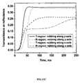
- the rubbing directions of both the first alignment film 909 a and the second alignment film 909 b affect the image brightness and dynamic response speed.
- the strip electrode design of FIG. 13B as an example, if the rubbing direction is along x-axis direction, which is perpendicular to the strip direction of the reflector pattern 907 , then the rise period response speed of both the reflective display mode and the transmissive display mode are slow.
- FIG. 15A shows the section view of the equilibrium state director distribution with the strip electrode design of FIG. 13B when rubbing direction is along x-axis direction.
- the liquid crystal molecules in the transmissive display region 912 will tilt along the x-axis direction first and those in the reflective display region 913 are pushed and pressed. Contrarily, the reoriented liquid molecules in the reflective display region 913 push and press the liquid molecules in the transmissive display region 912 . As a result of the interaction, the liquid crystal molecules on the border of the reflective display region 913 and the transmissive display region 912 deviate out of the x-z plane. In other words, a twist deformation evolution occurs on the border of the reflective display region 913 and the transmissive display region 912 .
- FIG. 15B shows the section view of the equilibrium state director distribution with the strip electrode design of FIG. 13B when rubbing direction is along y-axis direction.
- FIG. 15C shows the rise period dynamic response for different rubbing direction cases.
- the rubbing angle is preferably parallel to the strip direction of the reflector pattern.
- the apparatus, method, system and device of the present invention provides a new transflective LCD design with uniform cell gap configuration throughout the transmissive and reflective display regions.
- Use of a mutually complementary common electrode pattern and reflector pattern or mutually complementary ITO pixel electrode pattern and reflector pattern produces an electric field in the transmissive display region that is a uniform longitudinal field while the electric field in the reflective display region is a fringing field. Therefore, the initially vertically aligned negative dielectric anisotropic nematic liquid crystal material forms a smaller tilt angle with respect to the substrate normal in the reflective display region and simultaneously a larger tilt angle with respect to the substrate normal in the transmissive display region.
- the ambient incident light experiences a reduced phase retardation in the reflective display region while the light from the backlight source experiences an increased phase retardation. Since the ambient light passes through the reflective display region twice while the light from the backlight source only passes through the transmissive display region once, by properly designing the electrodes and the reflector width, the light from both ambient light source and backlight source experience approximately the same phase retardation in both reflective and transmissive display regions. As a result, the electro-optical performance curves of both transmissive display mode and reflective display mode overlap.
Abstract
Description
| 10 | transflective LCD design (U.S. | ||
| Pat. No. 4,315,258) | |||
| 11 | |
||
| 12 | |
||
| 13 | |
||
| 14 | |
||
| 15 | |
||
| 200 | transflective LCD design (U.S. | ||
| Pat. No. 6,281,952) | |||
| 201a | top linear polarizer | ||
| 201b | bottom linear polarizer | ||
| 202a | top compensation film | ||
| 202b | bottom compensation film | ||
| 203a | top transparent substrate | ||
| 203b | bottom transparent substrate | ||
| 204a | transparent electrode | ||
| 204b | transparent electrode | ||
| 205a | first alignment film | ||
| 205b | second alignment film | ||
| 206 | isolation layer | ||
| 207 | reflection layer | ||
| 208 | liquid crystal layer | ||
| 209 | backlight source | ||
| 210 | reflective display region | ||
| 211 | transmissive display region | ||
| 212 | transflector means | ||
| 300 | transflective LCD w/partial | ||
| switching (U.S. patent application No. | |||
| 20030202139) | |||
| 301a | top substrate | ||
| 301b | bottom substrate | ||
| 302 | transparent electrode | ||
| 303a | alignment film | ||
| 303b | alignment film | ||
| 304 | transflector means | ||
| 304a | non-patterned transparent electrode | ||
| 304b | patterned transparent electrode | ||
| 304c | reflector | ||
| 304d | insulating layer | ||
| 305 | liquid crystal layer | ||
| 305a | liquid crystal molecules | ||
| 305b | liquid crystal molecules | ||
| 306 | transmissive region | ||
| 307 | reflective region | ||
| 400 | transflective LCD, the first | ||
| embodiment of the present invention | |||
| 401a | first polarizer | ||
| 401b | second polarizer | ||
| 402a | first half-wave retardation film | ||
| 402b | second half-wave retardation film | ||
| 403a | first quarter-wave retardation film | ||
| 403b | second quarter-wave retardation film | ||
| 404 | negative birefringence c-film | ||
| 405a | first transparent substrate | ||
| 405b | second transparent substrate | ||
| 406a | patterned ITO layer | ||
| 406b | non-patterned ITO layer | ||
| 407 | patterned reflector | ||
| 408a | first non-conductive planar layer | ||
| 408b | second non-conductive planar layer | ||
| 409a | first vertical alignment film | ||
| 409b | second vertical alignment film | ||
| 410 | vertically aligned negative | ||
| dielectric anisotropic nematic LC layer | |||
| 411 | backlight source | ||
| 412 | transmissive display region | ||
| 413 | reflective display region | ||
| 701 | empty area | ||
| 900 | transmissive LCD, the second | ||
| embodiment of the present invention | |||
| 901a | first polarizer | ||
| 901b | second polarizer | ||
| 902a | first half-wave retardation film | ||
| 902b | second half-wave retardation film | ||
| 903a | first quarter-wave retardation film | ||
| 903b | second quarter-wave retardation film | ||
| 904 | negative birefringence c-film | ||
| 905a | first transparent substrate | ||
| 905b | second transparent substrate | ||
| 906a | non-patterned ITO layer | ||
| 906b | patterned ITO layer | ||
| 907 | patterned reflector | ||
| 908 | non-conductive planar layer | ||
| 909a | first vertical alignment film | ||
| 909b | second vertical alignment film | ||
| 910 | vertically aligned negative | ||
| dielectric anisotropic nematic liquid | |||
| crystal layer | |||
| 911 | backlight source | ||
| 912 | transmissive display region | ||
| 913 | reflective display region | ||
| TABLE 1 |
| The parameters of MLC-6608 liquid crystal mixture |
| K11 | 16.7 × 10⁻¹² N | ||
| K22 | 7.0 × 10⁻¹² N | ||
| K33 | 18.1 × 10⁻¹² N | ||
| ε// | 3.6 | ||
| ε⊥ | 7.8 | ||
| ne | 1.5606 (at λ = 550 nm) | ||
| no | 1.4770 (at λ = 550 nm) | ||
Claims (15)
Priority Applications (5)
| Application Number | Priority Date | Filing Date | Title |
|---|---|---|---|
| US11/110,229 US7339641B2 (en) | 2005-04-20 | 2005-04-20 | Transflective liquid crystal display with fringing and longitudinal electric field |
| PCT/US2006/013240 WO2006115748A2 (en) | 2005-04-20 | 2006-04-10 | Transflective liquid crystal display with vertical alignment |
| CNB2006100792913A CN100468139C (en) | 2005-04-20 | 2006-04-20 | Transflective liquid crystal display and its production method |
| TW095114128A TWI352864B (en) | 2005-04-20 | 2006-04-20 | Transflective liquid crystal display devices and f |
| US11/975,230 US7969540B2 (en) | 2005-04-20 | 2007-10-18 | Transflective liquid crystal display having mutually complementary patterned electrode and reflector |
Applications Claiming Priority (1)
| Application Number | Priority Date | Filing Date | Title |
|---|---|---|---|
| US11/110,229 US7339641B2 (en) | 2005-04-20 | 2005-04-20 | Transflective liquid crystal display with fringing and longitudinal electric field |
Related Child Applications (1)
| Application Number | Title | Priority Date | Filing Date |
|---|---|---|---|
| US11/975,230 Division US7969540B2 (en) | 2005-04-20 | 2007-10-18 | Transflective liquid crystal display having mutually complementary patterned electrode and reflector |
Publications (2)
| Publication Number | Publication Date |
|---|---|
| US20060238675A1 US20060238675A1 (en) | 2006-10-26 |
| US7339641B2 true US7339641B2 (en) | 2008-03-04 |
Family
ID=37186467
Family Applications (2)
| Application Number | Title | Priority Date | Filing Date |
|---|---|---|---|
| US11/110,229 Expired - Fee Related US7339641B2 (en) | 2005-04-20 | 2005-04-20 | Transflective liquid crystal display with fringing and longitudinal electric field |
| US11/975,230 Expired - Fee Related US7969540B2 (en) | 2005-04-20 | 2007-10-18 | Transflective liquid crystal display having mutually complementary patterned electrode and reflector |
Family Applications After (1)
| Application Number | Title | Priority Date | Filing Date |
|---|---|---|---|
| US11/975,230 Expired - Fee Related US7969540B2 (en) | 2005-04-20 | 2007-10-18 | Transflective liquid crystal display having mutually complementary patterned electrode and reflector |
Country Status (4)
| Country | Link |
|---|---|
| US (2) | US7339641B2 (en) |
| CN (1) | CN100468139C (en) |
| TW (1) | TWI352864B (en) |
| WO (1) | WO2006115748A2 (en) |
Cited By (5)
| Publication number | Priority date | Publication date | Assignee | Title |
|---|---|---|---|---|
| US20060170846A1 (en) * | 2005-02-03 | 2006-08-03 | Seiko Epson Corporation | Liquid crystal display and electronic apparatus |
| US20070046869A1 (en) * | 2005-08-23 | 2007-03-01 | Au Optronics Corporation | Liquid crystal display and method for manufacturing the same |
| US20100097563A1 (en) * | 2008-07-01 | 2010-04-22 | Guomin Zhang | Liquid crystal display device and associated liquid crystal media for use in the same |
| US10234721B2 (en) * | 2015-03-05 | 2019-03-19 | Shenzhen China Star Optoelectronics Technology Co., Ltd | Transflective liquid crystal display device and method of forming the same |
| US10386675B2 (en) * | 2016-09-26 | 2019-08-20 | Boe Technology Group Co., Ltd. | Display panel and display apparatus |
Families Citing this family (21)
| Publication number | Priority date | Publication date | Assignee | Title |
|---|---|---|---|---|
| JP4380648B2 (en) * | 2005-05-25 | 2009-12-09 | エプソンイメージングデバイス株式会社 | Liquid crystal device and electronic device |
| JP4466596B2 (en) * | 2006-03-29 | 2010-05-26 | カシオ計算機株式会社 | Orientation transition method |
| TWI354168B (en) | 2007-05-04 | 2011-12-11 | Au Optronics Corp | Optical compensation film, manufacturing method of |
| JP5324754B2 (en) * | 2007-05-10 | 2013-10-23 | スタンレー電気株式会社 | Liquid crystal display |
| CN101393335B (en) * | 2007-09-21 | 2011-09-28 | 群康科技(深圳)有限公司 | Half- penetration and half-reflection LCD |
| KR20090073387A (en) * | 2007-12-31 | 2009-07-03 | 엘지디스플레이 주식회사 | Liquid crystal display device |
| CN101526703B (en) * | 2008-03-04 | 2011-08-17 | 上海天马微电子有限公司 | Transmission and reflection liquid crystal display device |
| US8872180B2 (en) * | 2008-05-13 | 2014-10-28 | Sharp Kabushiki Kaisha | Liquid crystal display device and method for manufacturing liquid crystal display device |
| TWI402567B (en) * | 2009-07-14 | 2013-07-21 | Wintek Corp | Transflective liquid crystal display |
| CN102207643B (en) | 2010-03-29 | 2015-07-29 | 精工爱普生株式会社 | The driving method of liquid-crystal apparatus, liquid-crystal apparatus and electronic equipment |
| JP5654525B2 (en) * | 2011-09-30 | 2015-01-14 | 富士フイルム株式会社 | Liquid crystal display device and driving method of liquid crystal display device |
| CN103869541A (en) * | 2012-12-10 | 2014-06-18 | 京东方科技集团股份有限公司 | Half transparent and half reflecting liquid crystal display panel, manufacture method thereof, and liquid crystal display device |
| CN103176307B (en) * | 2013-03-26 | 2015-07-22 | 京东方科技集团股份有限公司 | Semi-transmissive semi-reflective liquid crystal display (LCD) panel and LCD device |
| CN103293770B (en) * | 2013-05-31 | 2015-12-23 | 京东方科技集团股份有限公司 | Display base plate and manufacture method and display panels |
| CN103676436B (en) * | 2013-12-20 | 2016-04-06 | 海信集团有限公司 | A kind of light source shaping methods for projecting and structure |
| CN104503143B (en) * | 2014-12-17 | 2017-09-26 | 深圳市华星光电技术有限公司 | A kind of transflective liquid crystal display and its manufacture method |
| EP3555692A4 (en) * | 2016-12-14 | 2020-07-08 | Université Laval | Method and apparatus for dynamically variable electrical control of light beam reflective liquid crystal devices |
| CN107102487B (en) * | 2017-07-06 | 2020-08-04 | 京东方科技集团股份有限公司 | Array substrate, manufacturing method thereof and reflective liquid crystal display device |
| KR102301279B1 (en) * | 2017-07-18 | 2021-09-13 | 삼성에스디아이 주식회사 | Polarizing plate and optical display device comprising the same |
| TWI769735B (en) * | 2020-11-18 | 2022-07-01 | 廖正興 | Spatial light modulator for suppressing fringe field effect |
| CN217060711U (en) * | 2021-12-02 | 2022-07-26 | 中强光电股份有限公司 | Display device |
Citations (10)
| Publication number | Priority date | Publication date | Assignee | Title |
|---|---|---|---|---|
| US4315258A (en) | 1980-02-15 | 1982-02-09 | The United States Of America As Represented By The Secretary Of The Navy | Transmissive and reflective liquid crystal display |
| US5933207A (en) | 1995-10-23 | 1999-08-03 | Hughes Electronics Corporation | Reflective-type liquid crystal displays using mixed-mode twist nematic cells |
| US6208405B1 (en) * | 1997-10-06 | 2001-03-27 | Samsung Electronics Co., Ltd. | Method for manufacturing a liquid crystal display |
| US6281952B1 (en) | 1997-12-26 | 2001-08-28 | Sharp Kabushiki Kaisha | Liquid crystal display |
| US20020180911A1 (en) * | 2001-03-28 | 2002-12-05 | Seiko Epson Corporation | Liquid-crystal display device and electronic equipment |
| US20030202139A1 (en) | 2002-04-30 | 2003-10-30 | Choi Wing Kit | Transflective liquid crystal display with partial switching |
| US20040155999A1 (en) * | 2003-01-24 | 2004-08-12 | Seiko Epson Corporation | Liquid crystal display device and electronic apparatus |
| US20040189903A1 (en) * | 2003-03-25 | 2004-09-30 | Alps Electric Co., Ltd. | Transflective film and liquid crystal display device |
| US20050231666A1 (en) * | 2004-04-16 | 2005-10-20 | Samsung Electronics Co., Ltd | Array substrate, manufacturing method thereof and display device having the same |
| US20050248693A1 (en) * | 2004-05-06 | 2005-11-10 | Hayato Kurasawa | Liquid crystal display device and electronic device |
Family Cites Families (3)
| Publication number | Priority date | Publication date | Assignee | Title |
|---|---|---|---|---|
| JP4489346B2 (en) * | 2002-12-17 | 2010-06-23 | シャープ株式会社 | Liquid crystal display |
| JP4338511B2 (en) * | 2003-12-24 | 2009-10-07 | シャープ株式会社 | Liquid crystal display |
| US7239365B2 (en) * | 2004-11-09 | 2007-07-03 | Tpo Displays Corp. | Transflective liquid crystal display |
-
2005
- 2005-04-20 US US11/110,229 patent/US7339641B2/en not_active Expired - Fee Related
-
2006
- 2006-04-10 WO PCT/US2006/013240 patent/WO2006115748A2/en active Search and Examination
- 2006-04-20 CN CNB2006100792913A patent/CN100468139C/en not_active Expired - Fee Related
- 2006-04-20 TW TW095114128A patent/TWI352864B/en not_active IP Right Cessation
-
2007
- 2007-10-18 US US11/975,230 patent/US7969540B2/en not_active Expired - Fee Related
Patent Citations (10)
| Publication number | Priority date | Publication date | Assignee | Title |
|---|---|---|---|---|
| US4315258A (en) | 1980-02-15 | 1982-02-09 | The United States Of America As Represented By The Secretary Of The Navy | Transmissive and reflective liquid crystal display |
| US5933207A (en) | 1995-10-23 | 1999-08-03 | Hughes Electronics Corporation | Reflective-type liquid crystal displays using mixed-mode twist nematic cells |
| US6208405B1 (en) * | 1997-10-06 | 2001-03-27 | Samsung Electronics Co., Ltd. | Method for manufacturing a liquid crystal display |
| US6281952B1 (en) | 1997-12-26 | 2001-08-28 | Sharp Kabushiki Kaisha | Liquid crystal display |
| US20020180911A1 (en) * | 2001-03-28 | 2002-12-05 | Seiko Epson Corporation | Liquid-crystal display device and electronic equipment |
| US20030202139A1 (en) | 2002-04-30 | 2003-10-30 | Choi Wing Kit | Transflective liquid crystal display with partial switching |
| US20040155999A1 (en) * | 2003-01-24 | 2004-08-12 | Seiko Epson Corporation | Liquid crystal display device and electronic apparatus |
| US20040189903A1 (en) * | 2003-03-25 | 2004-09-30 | Alps Electric Co., Ltd. | Transflective film and liquid crystal display device |
| US20050231666A1 (en) * | 2004-04-16 | 2005-10-20 | Samsung Electronics Co., Ltd | Array substrate, manufacturing method thereof and display device having the same |
| US20050248693A1 (en) * | 2004-05-06 | 2005-11-10 | Hayato Kurasawa | Liquid crystal display device and electronic device |
Cited By (12)
| Publication number | Priority date | Publication date | Assignee | Title |
|---|---|---|---|---|
| US20060170846A1 (en) * | 2005-02-03 | 2006-08-03 | Seiko Epson Corporation | Liquid crystal display and electronic apparatus |
| US7420635B2 (en) * | 2005-02-03 | 2008-09-02 | Seiko Epson Corporation | Liquid crystal display and electronic apparatus having a quasi-isotropic liquid crystal material |
| US20080316403A1 (en) * | 2005-02-03 | 2008-12-25 | Seiko Epson Corporation | Liquid crystal display and electronic apparatus |
| US7639327B2 (en) | 2005-02-03 | 2009-12-29 | Seiko Epson Corporation | Liquid crystal display and electronic apparatus having a quasi-isotropic liquid crystal material |
| US20070046869A1 (en) * | 2005-08-23 | 2007-03-01 | Au Optronics Corporation | Liquid crystal display and method for manufacturing the same |
| US7688407B2 (en) * | 2005-08-23 | 2010-03-30 | Au Optronics Corporation | Liquid crystal display with transmissive and reflective regions comprising a first alignment film having different alignments in the transmissive and reflective regions and a second alignment film with a single alignment |
| US20100139856A1 (en) * | 2005-08-23 | 2010-06-10 | Au Optronics Corporation | Method for Manufacturing a Liquid Crystal Display |
| US7830482B2 (en) | 2005-08-23 | 2010-11-09 | Au Optronics Corporation | Method for manufacturing a transflective liquid crystal display panel comprising forming a first alignment film having different alignments in the transmissive and reflective regions and forming a second alignment film with a single alignment |
| US20100097563A1 (en) * | 2008-07-01 | 2010-04-22 | Guomin Zhang | Liquid crystal display device and associated liquid crystal media for use in the same |
| US8848158B2 (en) * | 2008-07-01 | 2014-09-30 | Gentex Corporation | Liquid crystal display device and associated liquid crystal media for use in the same |
| US10234721B2 (en) * | 2015-03-05 | 2019-03-19 | Shenzhen China Star Optoelectronics Technology Co., Ltd | Transflective liquid crystal display device and method of forming the same |
| US10386675B2 (en) * | 2016-09-26 | 2019-08-20 | Boe Technology Group Co., Ltd. | Display panel and display apparatus |
Also Published As
| Publication number | Publication date |
|---|---|
| WO2006115748A2 (en) | 2006-11-02 |
| TW200707028A (en) | 2007-02-16 |
| TWI352864B (en) | 2011-11-21 |
| CN1916703A (en) | 2007-02-21 |
| US20080043188A1 (en) | 2008-02-21 |
| US7969540B2 (en) | 2011-06-28 |
| WO2006115748A3 (en) | 2007-12-13 |
| CN100468139C (en) | 2009-03-11 |
| US20060238675A1 (en) | 2006-10-26 |
Similar Documents
| Publication | Publication Date | Title |
|---|---|---|
| US7339641B2 (en) | Transflective liquid crystal display with fringing and longitudinal electric field | |
| JP4380648B2 (en) | Liquid crystal device and electronic device | |
| US7995168B2 (en) | Transflective liquid crystal display having a relationship between the electrode spacing and cell gap in the reflection and transmission regions | |
| US7251000B2 (en) | Transflective LCD having a reflective film overlapping the transmissive area and alignment regulators in plan view | |
| US7259816B2 (en) | Liquid crystal display device and electronic apparatus | |
| KR100806475B1 (en) | Liquid crystal display device and electronic apparatus | |
| CN100443968C (en) | Liquid crystal device and electronic apparatus | |
| KR100921600B1 (en) | Liquid crystal display device | |
| US7126657B2 (en) | Multi-domain transflective liquid crystal display with plurality of band-shaped reflectors | |
| JP5019848B2 (en) | Liquid crystal device and electronic device | |
| US7106407B2 (en) | Liquid crystal display device and electronic apparatus | |
| JP3900141B2 (en) | Liquid crystal display device and electronic device | |
| JP2004085918A (en) | Liquid crystal display device, method for manufacturing same, and electronic apparatus | |
| US20040061817A1 (en) | Liquid crystal display device and electronic apparatus | |
| JP2000047194A (en) | Liquid crystal display device | |
| TWI364589B (en) | Vertical alignment mode reflective-transmissive liquid crystal display with multi cell gap | |
| CN114326197A (en) | Display panel and display device | |
| JP2003140154A (en) | Liquid crystal display device | |
| TWI385436B (en) | Transflective liquid crystal display | |
| JP4697122B2 (en) | Liquid crystal display device and electronic device | |
| KR20060110928A (en) | Transflective type liquid crystal display device | |
| JP4905242B2 (en) | Liquid crystal device and electronic device | |
| JP4479717B2 (en) | Liquid crystal display device and electronic device | |
| JP2004198921A (en) | Liquid crystal display device and electronic appliance | |
| JP2009151271A (en) | Liquid crystal display device |
Legal Events
| Date | Code | Title | Description |
|---|---|---|---|
| AS | Assignment |
Owner name: RESEARCH FOUNDATION OF THE UNIVERISTY OF CENTRAL F Free format text: ASSIGNMENT OF ASSIGNORS INTEREST;ASSIGNORS:SHU, XINYU;GE, ZHIBING;WU, SHIN-TSON;REEL/FRAME:016496/0013 Effective date: 20050414 |
|
| AS | Assignment |
Owner name: RESEARCH FOUNDATION OF THE UNIVERSITY OF CENTRAL F Free format text: CORRECTIVE ASSIGNMENT TO CORRECT THE 1ST CONVEYING PARTY'S NAME AND BOTH THE RECEIVING PARTIES. DOCUMENT PREVIOUSLY RECORDED AT REEL 016496 FRAME 0013;ASSIGNORS:ZHU, XINYU;GE, ZHIBING;WU, SHIN-TSON;REEL/FRAME:019934/0177 Effective date: 20050814 Owner name: TOPPOLY OPTOELECTRONICS CORP., TAIWAN Free format text: CORRECTIVE ASSIGNMENT TO CORRECT THE 1ST CONVEYING PARTY'S NAME AND BOTH THE RECEIVING PARTIES. DOCUMENT PREVIOUSLY RECORDED AT REEL 016496 FRAME 0013;ASSIGNORS:ZHU, XINYU;GE, ZHIBING;WU, SHIN-TSON;REEL/FRAME:019934/0177 Effective date: 20050814 |
|
| AS | Assignment |
Owner name: TPO DISPLAYS CORP., TAIWAN Free format text: CHANGE OF NAME;ASSIGNOR:TOPPOLY OPTOELECTRONICS CORP.;REEL/FRAME:025584/0544 Effective date: 20060605 |
|
| AS | Assignment |
Owner name: CHIMEI INNOLUX CORPORATION, TAIWAN Free format text: MERGER;ASSIGNOR:TPO DISPLAYS CORP.;REEL/FRAME:025918/0759 Effective date: 20100318 |
|
| FPAY | Fee payment |
Year of fee payment: 4 |
|
| AS | Assignment |
Owner name: INNOLUX CORPORATION, TAIWAN Free format text: CHANGE OF NAME;ASSIGNOR:CHIMEI INNOLUX CORPORATION;REEL/FRAME:032604/0487 Effective date: 20121219 |
|
| REMI | Maintenance fee reminder mailed | ||
| LAPS | Lapse for failure to pay maintenance fees | ||
| STCH | Information on status: patent discontinuation |
Free format text: PATENT EXPIRED DUE TO NONPAYMENT OF MAINTENANCE FEES UNDER 37 CFR 1.362 |
|
| FP | Lapsed due to failure to pay maintenance fee |
Effective date: 20160304 |