US7295051B2 - System and method for monitoring a power supply level - Google Patents
System and method for monitoring a power supply level Download PDFInfo
- Publication number
- US7295051B2 US7295051B2 US11/153,773 US15377305A US7295051B2 US 7295051 B2 US7295051 B2 US 7295051B2 US 15377305 A US15377305 A US 15377305A US 7295051 B2 US7295051 B2 US 7295051B2
- Authority
- US
- United States
- Prior art keywords
- bit
- power supply
- power
- status register
- recited
- Prior art date
- Legal status (The legal status is an assumption and is not a legal conclusion. Google has not performed a legal analysis and makes no representation as to the accuracy of the status listed.)
- Active
Links
Images


Classifications
-
- G—PHYSICS
- G06—COMPUTING; CALCULATING OR COUNTING
- G06F—ELECTRIC DIGITAL DATA PROCESSING
- G06F1/00—Details not covered by groups G06F3/00 - G06F13/00 and G06F21/00
- G06F1/26—Power supply means, e.g. regulation thereof
- G06F1/28—Supervision thereof, e.g. detecting power-supply failure by out of limits supervision
Definitions
- This invention relates to power supply monitoring schemes and, more particularly, to a circuit and method for monitoring the integrity of a power supply by monitoring a level of the power supply.
- PLDs programmable logic devices
- internal memory cells, registers and configuration state machines of the device may all be initialized according to specific power-up reset sequences.
- the configuration state machine may take control of the configuration process by loading configuration data into volatile memory cells. When all of the data has been loaded, the I/O pins of the PLD are enabled and the device is ready to begin performing its programmed function.
- Another reset process takes place when a device is powered down, i.e., when the power supply voltage is brought down from the operating voltage level to the zero power state (or below a triggering voltage level).
- the PLD may detect that the power supply voltage has reached or is nearing an unacceptably low level. If detected, the PLD performs a sequence of operations such as saving current memory cell, register and state machine information, informing other integrated circuits to stop sending data to the PLD, and so forth.
- the power-up and power-down reset procedures are complicated by the fact that power supplies can be noisy, sometimes glitching significantly above and/or below a triggering voltage level.
- the PLD or another power-dependent component
- the PLD is included within a computer system that shares a power supply line with various appliances (such as an air conditioner, electric drill, etc.).
- appliances such as an air conditioner, electric drill, etc.
- a large current spike may be introduced into the shared supply line when one or more of the appliances are turned on. If the current spike causes the supply line voltage to drop below the acceptable operating voltage level, the PLD may lose volatile information (such as register and memory content) or may enter the wrong configuration state.
- other types of power failure (such as temporary loss of power) may produce the same results by not giving the PLD enough time to perform a proper power-down sequence.
- a reset signal is typically asserted (i.e., “ON”) when the power supply voltage is rising towards the acceptable operating voltage level, and deasserted (i.e., “OFF”) once the power supply voltages reaches the acceptable level.
- the power-down reset sequence is similar; however, the reset signal is asserted once the power supply voltage falls below an unacceptable operating voltage level, and deasserted once the power supply voltage reaches the zero power state. To operate properly, both reset sequences must be asserted for a specific duration of time needed to perform the power-up or power-down sequence of operations.
- Most conventional systems include at least one power-on reset (POR) circuit for monitoring the power supply voltage and generating a reset signal, in accordance with a power-up and/or power-down reset operation.
- the POR circuit may also be implemented to ensure that the reset signals are asserted for the required duration.
- Most POR circuits are based on circuits comprising resistors and capacitors (e.g., RC POR circuits) or, in some cases, voltage comparators comprising voltage dividers and voltage reference generators (e.g., bandgap POR circuits). All provide an active high (or active low) reset signal to one or more system components, indicating that they should perform the necessary power-up or power-down reset functions.
- none of the conventional POR circuits provide indication as to the cause behind the reset signal, thus, leaving the circuit designer or user in the dark as to the reason for the power failure.
- the problems outlined above may be in large part addressed by an improved system and method for monitoring the integrity of a power supply by monitoring the state of one or more bits stored within a status register. If the state of the one or more bits changes, e.g., from a “set state” to a “cleared state,” a circuit designer or user of the system may conclude that a power abnormality has occurred, rather than a normal power-up or power-down operation.
- a method for monitoring a power supply level, such method comprising: setting a bit in a status register after the power supply level reaches a threshold level, and monitoring a state of the bit to determine if the power supply level has dropped below the threshold level.
- the method may perform one or more steps prior to the step of setting the first bit.
- the method may include: clearing the bit in response to a power-on/reset of a system, and monitoring an output signal supplied from a power-on/reset (POR) circuit associated with the system.
- POR power-on/reset
- the bit may be initially set sometime after system power-up.
- the state of the bit may be changed (i.e., from a “set state” to a “cleared state”) if a subsequent output signal supplied from the POR circuit comprises an asserted power-on/reset signal. If the state of the bit changes from a “set state” to a “cleared state,” the circuit designer or user of the system may conclude that a power abnormality has occurred, and that the abnormality is caused by the level of the power supply dropping below the threshold level.
- a system for monitoring a power supply voltage level, such system comprising: a power-on/reset (POR) circuit configured for generating a reset signal, and a status register configured for storing a bit, having a first logic state, in response to the generated reset signal.
- POR power-on/reset
- the POR circuit may generate an asserted reset signal once the power supply voltage level begins ramping up towards a threshold voltage level, whereas a deasserted reset signal may be generated upon reaching the threshold voltage level.
- the POR circuit may generate a subsequent reset signal in response the power supply voltage level dropping and then ramping back up towards the threshold voltage level.
- the bit stored within the status register may be changed from the first logic state to a second logic state, different from the first.
- Means are also included within the system for monitoring the stored bit and determining that the power supply voltage level has dropped below the threshold level, if the bit stored within the status register changes from the first logic state to the second logic state.
- the means for monitoring the stored bit and determining that the power supply voltage level has dropped below the threshold voltage level may include hardware-implemented logic located internal to the system and having access to the stored bit via a bus.
- said means may include software-implemented logic stored as program instructions on a computer-readable medium and executed by a processor of the system.
- the system processor may have access to the stored bit via the bus.
- the status register may be implemented with an I2C register and the bus may be implemented with an I2C bus.
- Alternative means for storing a bit are contemplated herein.
- FIG. 1A is a circuit diagram of an exemplary RC power-on/reset (POR) circuit
- FIG. 1B is a graph of an exemplary output waveform generated by the POR circuit of FIG. 1A ;
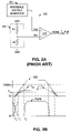
- FIG. 2A is a schematic diagram of an exemplary bandgap power-on/reset (POR) circuit
- FIG. 2B is a graph illustrating an exemplary output waveform generated by the POR circuit of FIG. 2A ;
- FIG. 3 is a block diagram of an exemplary system including a system power supply, a POR circuit, a status register, and exemplary circuits and methods for monitoring the integrity of the system power supply by detecting a state of one or more bits stored within the status register;
- FIG. 4 is a flowchart diagram illustrating the exemplary methods for monitoring the integrity of the system power supply
- FIG. 5-6 are schematic diagrams of exemplary circuits configured for monitoring the integrity of an electrical connection between the system power supply and a power supply pin, according to various embodiment of the invention.
- FIGS. 7-8 are schematic diagrams of exemplary circuits configured for monitoring the integrity of an electrical connection between a ground supply and a ground supply pin, according to various embodiments of the invention.
- FIG. 1A illustrates one embodiment of a power-on reset (POR) circuit 100 that uses an RC structure to provide a reset signal to one or more system components based on a level of the power supply voltage (VDD).
- VDD power supply voltage
- the RC POR circuit of FIG. 1A includes a pull-up transistor (PU), a resistor (R), a capacitor (C), and inverters (I 1 , I 2 , I 3 ).
- the number of inverters on the output path varies according to whether an active low or active high reset signal is desired.
- an active low reset signal PORB
- the PORB signal may be supplied to one or more system components for performing a power-up or power-down reset sequence.
- the PORB signal may be inverted (e.g., by inverter I 3 ) to provide an active high reset signal (POR).
- FIG. 1B illustrates one manner in which the POR circuit of FIG. 1A may generate an active low reset signal (PORB) based on a level of the power supply voltage (VDD).
- VDD power supply voltage
- V min the minimum voltage threshold
- POR circuit 100 to generate an active low (PORB) reset signal.
- the PORB reset signal goes high (inactive) once VDD reaches an acceptable operating voltage level (VPOR+) at time T 2 .
- the duration between times T 1 and T 2 needs to be at least as long as the power-up sequence.
- the PORB reset signal may go low (active) again, e.g., when VDD falls below an unacceptable operating voltage level (VPOR ⁇ ) at time T 3 .
- the PORB reset signal becomes active soon thereafter (at time T 4 ) when VDD rises back up to the acceptable voltage level.
- the sharp decrease in VDD may be attributed to a “glitch” in the power supply.
- the time duration between times T 3 and T 4 may not be long enough for the system components to perform a proper reset sequence.
- the rising POR voltage (VPOR+) is different from the falling POR voltage (VPOR ⁇ ). This difference is typically due to the difference between the charging and discharging times of capacitor C.
- FIG. 2A illustrates an alternative embodiment of a power-on reset (POR) circuit 200 that generates a reset signal by comparing the power supply voltage (VDD) to a reference voltage (Vref).
- POR circuit 200 may include a comparator for comparing the power supply voltage (divided down using a resistor divider network) to a reference voltage (also derived from VDD). As VDD ramps up to a predetermined level, the value of the reset signal (POR) on the output terminal of POR circuit 200 also rises. When the divided voltage (Vdiv) rises above the reference voltage (Vref), the comparator drives the reset signal low (i.e., inactive) again.
- the POR circuit of FIG. 2A includes an analog comparator 210 having a positive input terminal and a negative input terminal.
- a reference voltage generator 220 supplies the reference voltage (Vref) to the negative terminal of the comparator.
- reference voltage generator 220 may be implemented with a bandgap reference circuit, in which case, POR circuit 200 may be referred to as a “bandgap POR circuit.”
- Voltage divider 230 may include resistors R 1 and R 2 for dividing down the power supply voltage (VDD) to a predetermined fraction (Vdiv), which is supplied to the positive terminal of the comparator. As known in the art, the voltage provided by voltage divider 230 would be [R 2 /(R 1 +R 2 )]*VDD.
- comparator 210 provides an active low (PORB) reset signal once VDD begins to rise; the PORB signal is deasserted (inactive) once the divided voltage (Vdiv) surpasses the reference voltage (Vref).
- inverter I 4 may be included to provide an active high (POR) reset signal.
- FIG. 2B illustrates one manner in which the POR circuit of FIG. 2A may generate an active low reset signal (PORB) based on a level of the power supply voltage (VDD).
- the power supply voltage (VDD) begins to rise at time, T 0 ′.
- the power supply voltage rises past the trigger point (i.e., the minimum voltage threshold, V min ), causing POR circuit 200 to generate an active low (PORB) reset signal.
- the PORB reset signal goes high (inactive) once the divided voltage (Vdiv) surpasses the reference voltage (Vref) at time T 2 ′
- the duration between times T 1 ′ and T 2 ′ needs to be at least as long as the power-up sequence.
- the rising POR voltage (VPOR+) is the same as the falling POR voltage (VPOR ⁇ ). This is because the POR voltage, rising or falling, depends on a digital output signal from comparator 210 , not on the charging and discharging of a (sometimes large) capacitor.
- POR circuits 100 and 200 are capable of generating a reset signal to initiate a power related event (such as a power-up or power-down reset operation), circuits 100 and 200 are not capable of determining a cause (e.g., power-up, power-down, a glitch or temporary loss of power) for such initiation.
- the reset signals are simply supplied to one or more system components, indicating that the necessary power-up or power-down functions should be performed.
- the POR circuits of FIGS. 1 and 2 provide no resources or additional information that would enable a circuit designer or user of the system to diagnose an underlying power-related problem. In other words, conventional POR circuits provide no means for monitoring the integrity of a power supply.
- FIG. 3 is a block diagram of an exemplary system 300 including a system power supply 310 , a conventional POR circuit 320 , and various circuits and methods for monitoring the integrity of the power supply voltage (VDD) supplied to one or more system components 330 , 332 , 334 , 336 .
- VDD power supply voltage
- the circuits and methods described herein may be configured for monitoring the integrity of the power supply by detecting a state of one or more bits stored within a status register 340 of the system. The stored bits may be later read, via a system processor or other component 350 , for determining a cause of the power related event.
- system 300 may represent a portion of a computer system or a standalone chip configured for performing a particular function.
- system 300 may represent a portion of any chip having an on-chip register, which can be read via a serial or a parallel bus.
- system 300 may be included within a clock generation chip, which may in turn be incorporated within a computer system.
- system power supply 310 may comprise one or more supply pins for receiving a power supply voltage (VPWR, VDD), and in some cases, a ground supply voltage (VSS) from an external source.
- VPWR, VDD power supply voltage
- VSS ground supply voltage
- system power supply 310 may include a voltage generator for transforming the received power supply voltage (VPWR) into one or more voltage levels (VDD) used by internal chip or system components.
- the received or generated voltage level(s) may be supplied to various system components for operating those components.
- the received or generated voltage level(s) may be supplied to a volatile or non-volatile memory array 330 , one or more internal registers 332 , a configuration state machine 334 and/or other integrated circuits (IC's) located within the chip or system.
- power-on reset (POR) circuit 320 may be coupled to system power supply 310 for monitoring the voltage level supplied to system components 330 , 332 , 334 , 336 .
- POR circuit 320 may supply a RESET signal to the system components during normal power-up and power-down operations, as well as abnormal power related situations caused, e.g., by glitches in the power supply or even a temporary loss of power.
- POR circuit 320 may be implemented by any means known in the art (including those shown in FIGS. 1A and 2A ), since the generation of a RESET signal is well known and not intended as a novelty of the present invention.
- an advantage of the present invention is the ability to use the circuits and methods described herein with substantially any POR circuit known in the art, enabling the described circuits and methods to be easily incorporated within existing chip or system designs.
- the RESET signal generated by POR circuit 320 is supplied to status register 340 for clearing a “power good” (PWRGD) bit stored therein.
- the RESET signal is de-asserted once system power supply 310 becomes stable.
- the PWRGD bit may be asserted (e.g., set to logic HIGH) to indicate that the power supply voltage level has reached an acceptable operating voltage level.
- the PWRGD bit may be set automatically by logic components (included, e.g., within PSM 360 ), or manually by a user of the system, once the power supply voltage becomes stable. After the PWRGD bit achieves a “set state,” the bit may be monitored for any changes.
- a change in the PWRGD bit from a “set state” to a “cleared state” may indicate to the circuit designer or user that a power abnormality (e.g., a glitch or temporary loss of power) has occurred.
- a power abnormality e.g., a glitch or temporary loss of power
- the state of the PWRGD bit may be monitored by Power Supply Monitor (PSM) logic 360 located within the chip or system. Such monitoring may be performed at random, periodic and continuous intervals, as defined by the PSM logic. In a preferred embodiment, however, the state of the PWRGD bit may be monitored by a circuit designer or user of the system via the system processor or another system component 350 . Such monitoring may be performed at various intervals, as the user sees fit, or after the user is alerted to a problem with the system.
- the PWRGD bit may be stored within an I2C register 340 located on the periphery of the chip. As such, the state of the PWRGD bit may be accessible to the user via an I2C controller and a common I2C bus.
- status register 340 should not be limited to an I2C register, and may be alternatively implemented with substantially any storage means having read/write capability. Status register 340 may also be configured to include substantially any number and/or order of status and control bits, as deemed necessary.
- status register 340 can be maintained by supplying power to the status register from an independent power supply.
- the power supplied to status register 340 may be separate and distinct from the power supply (or supplies) to be monitored by PSM logic 360 .
- FIG. 4 illustrates exemplary methods 400 for monitoring the integrity of a power supply. More specifically, method 400 includes two distinct methods, which may be used separately or in conjunction with one another for monitoring the integrity of the power supply.
- the first method (denoted with subscript A) describes exemplary steps for monitoring a level of the power supply voltage.
- the second method (denoted with subscript B) describes exemplary steps for monitoring an electrical connection between the power supply (or ground supply) and one or more supply pins.
- Each of the methods involves monitoring a state of one or more bits stored in the status register 340 . The first method will now be described in more detail.
- An exemplary method 400 A for monitoring the power supply voltage level may begin, in most cases, during the initial power-on reset sequence initialization (step 410 A).
- a RESET signal is generated (e.g., by POR circuit 320 ) to indicate that the power supply is ramping up in voltage.
- the PWRDG bit is cleared in the status register (step 420 A) to clear the results from any previous monitoring cycles.
- POR circuit 320 may deactivate the RESET signal in step 430 A.
- the PWRGD bit is asserted (e.g., set to logic HIGH) in the status register 340 , indicating that the power supply voltage level has reached an acceptable operating voltage level (step 440 A).
- the PWRGD bit may be set by logic included within PSM 360 .
- the PWRGD bit may be set manually by a user of the system once the power supply voltage reaches the appropriate level (i.e., sometime after the RESET signal is initially detected).
- the state of the PWRGD bit is then monitored (step 450 A)—either automatically (via logic) or manually (via user interaction)—for changes.
- the step of monitoring may continue (either automatically or manually) if the PWRGD bit remains unchanged in the “set state” (step 460 A).
- POR circuit 320 may generate another RESET signal in response to a power-down reset sequence or in response to a power abnormality (such as a glitch or loss of power). If generated, the additional RESET signal may deassert the PWRGD bit (e.g., cleared to logic LOW) in the status register 340 , indicating that the power supply voltage level has fallen below an unacceptable operating voltage level.
- the circuit designer or user may assume that a power abnormality has occurred (such as a glitch or temporary loss of power), rather than a normal power-down reset sequence.
- the above method may provide the circuit designer or user with enough information to determine a cause of the power related event (step 470 A), simply by monitoring the PWRGD bit for changes from a “set state” to a “cleared state.”
- the above-mentioned method provides numerous advantages, including but not limited to, the ability to use an existing POR circuit without necessitating significant changes to the chip or board layout, and the ability to diagnose a cause of the power failure via a bit, which may be stored within a status register and read out later.
- the method may be performed by internally located PSM logic at random, periodic or continuous intervals, as defined by the internal logic.
- one or more steps of the method may be performed by a circuit designer or user of the system to conserve power and area, as well as to reduce design complexity.
- the method steps described above may be performed in response to an error signal (e.g., an indication of power failure) associated with the system.
- the system error signal may then prompt a user of the system to activate the PSM logic, or manually perform the above-mentioned steps, so that the cause of the error may be diagnosed.
- the above-mentioned method may be performed by a user of the system for substantially any reason and at substantially any time during or after system power-up.
- method 400 B may be implemented separately, or along with method 400 A, for monitoring an electrical connection between the system power supply (or ground supply) and one or more supply pins.
- another cause of power failure may be attributed to one or more supply pins (or contact pads) lifting off the board, or otherwise loosing electrical contact with the supply lines originating from the system power or ground supplies.
- a supply pin sensor 370 FIG. 3
- method 400 B FIG. 4
- An exemplary method 400 B for monitoring an electrical connection between the system power supply (or ground supply) and one or more supply pins (or contact pads) may begin, in most cases, during the initial power-on reset operation (step 410 B).
- one or more “pin enabled” (PIN_EN) bits may be cleared in the status register (step 420 B) to clear any results from previous monitoring cycles.
- the method may determine whether or not a sense enable signal is detected (step 430 B). In some cases, the sense enable signal may be asserted upon system power-up so that a faulty supply pin can be identified, e.g., if the power supply level never reaches the acceptable operational level (i.e., if a RESET signal is never generated by the POR circuit).
- the sense enable signal may be asserted at various intervals (e.g., randomly, periodically or continuously), or in response to an error signal associated with the system (e.g., an indication of system power failure). As such, the sense enable signal may be asserted by a user of the system, or in some cases, by additional logic (not shown) included within the system. Regardless, method 400 B may be temporarily suspended until the sense enable signal is detected in step 430 B.
- supply pin sensor 370 may detect whether or not an electrical connection exists between a supply potential and a respective supply pin by monitoring a voltage level supplied to a node coupled to the supply pin (step 435 B). If the voltage level is greater than, e.g., a threshold voltage of a CMOS gate, a pin enabled signal may be supplied to status register 340 for setting the appropriate PIN_EN bit (steps 440 B). Otherwise, a pin disabled signal may be supplied to status register 340 for clearing the appropriate PIN_EN bit (steps 440 B).
- step 460 B If the PIN_EN bit is asserted (e.g., set to logic HIGH) in step 460 B, the method may end (not shown) or continue with the step of monitoring the state of the one or more PIN_EN bits (step 450 B). However, if the PIN_EN bit is deasserted (e.g., cleared to logic LOW) in step 460 B, the circuit designer or user may conclude (step 470 B) that the supply pin corresponding to the cleared PIN_EN bit has lifted off the board supply. In other words, the circuit designer or user may assume that an electrical connection between the board supply and the supply pin (or contact pad) has been broken.
- the above-mentioned method provides numerous advantages, including but not limited to, the ability to diagnose a cause of power failure via a bit, which may be stored within a status register and read out later. Because supply pin sensor 370 is integrated “at the pad,” the above-mentioned method provides additional resources for diagnosing system power failures that may occur, e.g., before the power supply voltage has had a chance to reach the acceptable operating voltage level. This may be particularly advantageous to a circuit designer during the test and debugging phases of a chip or system design. For example, consider the case in which an internal power supply bus is sourced (i.e., supplied with power) by multiple power supply pins to minimize the resistance of the internal power supply bus.
- the chip may continue to function if at least one of the supply pins is still connected to the bus.
- Conventional methods which rely on precursory indications of chip failure, may fail to alert the circuit designer to a problem “at the pad.”
- the present method enables a circuit designer or user to detect whether any of the supply pins have lifted off the board, even when the chip continues to function.
- FIGS. 5-8 show exemplary circuit diagrams of supply pin sensor 370 , according to various embodiments of the invention.
- FIGS. 5-6 illustrate circuits for monitoring the integrity of an electrical connection between a power supply (e.g., system power supply 310 ) and one or more power supply pins.
- FIGS. 7-8 illustrate alternative embodiments of the invention, including circuits for monitoring the integrity of an electrical connection between a ground supply (not shown) and one or more ground supply pins.
- the power and ground supply pins are generally located on the periphery or top/bottom surfaces of a chip and may be implemented in a variety of ways including, but not limited to, pins, contact pads, solder bumps, etc.
- the term “supply pin” may be used herein to describe numerous means for connecting a power or ground supply potential to internal chip or system components.
- FIG. 5 illustrates one embodiment of a supply pin sensor circuit 500 for monitoring the integrity of an electrical connection between a power supply (not shown) and one or more power supply pins 510 .
- circuit 500 may be configured for monitoring only one power supply pin (such as the VDD core pin), and thus, may include only a portion of the elements shown in FIG. 5 .
- circuit 500 may include a p-channel field effect transistor (transistor Pc) whose source terminal is coupled to a VDD potential through the VDD core pin, and whose drain terminal is coupled to ground (i.e., a VSS potential) through a passive load (resistor Rc).
- transistor Pc p-channel field effect transistor
- a voltage develops at the node between the drain terminal of transistor Pc and resistor Rc. If the voltage at the drain terminal node is greater than the gate threshold voltage of transistor Pc, a pin enabled signal (e.g., an asserted PIN_EN_CORE) may be supplied to status register 340 for setting the appropriate PIN_EN bit therein. If the VDD core pin is not connected to the supply potential, the drain terminal of transistor Pc is pulled down to ground by load resistor Rc. If this occurs, a pin disabled signal (e.g., a deasserted PIN_EN_CORE) may be supplied to the status register for clearing the appropriate PIN_EN bit.
- SENSE_EN_CORE active low sense enable signal
- inverter Ic may be eliminated from the circuit diagram of FIG. 5 .
- buffer Bc may not be included in all embodiments of the invention for buffering the (asserted or deasserted) pin enable signal before it is sent to the status register.
- the sense enable signal may only be asserted at certain times, such as during system power up and/or when conducting a subsequent test of the power supply/pin connectivity.
- the sense enable signal may be deasserted to turn off transistor Pc and shut off the current flow to load resistor Rc. This can save power consumption within the chip.
- circuit 500 may be configured for monitoring the integrity of a plurality of supply pins (VDD core, VDD 1 . . . VDDN).
- the number of supply pins monitored may include a portion (or a total number) of the supply pins made available to the chip.
- circuit 500 may include a p-channel transistor (transistor Pc, P 1 . . . PN) coupled in series with a passive load (resistor Rc, R 1 . . . RN).
- a source terminal of the p-channel transistor may be coupled to a power supply potential through a respective power supply pin.
- the power supply potentials VDD 1 . . .
- VDDN may be substantially the same as, or different from, the core power supply potential (VDD core), depending on the needs of the various components included within the chip.
- the drain terminal of the p-channel transistor is coupled to ground (or a VSS potential) through a passive load, while the gate terminal is coupled for receiving the sense enable signal (SENSE_EN_CORE, SENSE_EN_ 1 . . . SENSE_EN_N). If the voltage present at the drain terminal of the p-channel transistor is greater than the gate threshold voltage of transistor Pc, an asserted pin enabled signal (PIN_EN_CORE, PIN_EN_ 1 . . . PIN_EN_N) is supplied to status register 340 , otherwise, a deasserted signal is supplied.
- each of the asserted/deasserted pin enabled signals may be used for setting/clearing a different PIN_EN bit within status register 340 .
- each of the plurality of pin enabled signals may be stored as a distinct bit within the status register to indicate whether or not an electrical connection exists between a power supply potential and a respective power supply pin.
- the plurality of pin enabled signals may be supplied to optional logic block 520 . If included, logic block 520 may generate a master pin enabled signal, which may be used for setting/clearing a single PIN_EN bit within status register 340 .
- the master pin enabled signal may be asserted when each of the plurality of pin enabled signals supplied thereto is asserted. In other cases, the master pin enabled signal may be asserted when at least one of the plurality of pin enabled signals is asserted. Other configurations/scenarios may be used.
- logic block 520 may limit the amount of information made available to the circuit designer or user by indicating whether or not an electrical connection exists between all power supply potentials and all power supply pins, or between at least one power supply potential and respective power supply pin. However, use of logic block 520 may advantageously reduce the number of status register bits required, thus, saving power, area and cost.
- the contents stored within status register 340 can be maintained by supplying power to the status register from an independent power supply.
- the power supplied to status register 340 may be separate and distinct from the power supply (or supplies) to be monitored by supply pin sensor circuit 500 .
- FIG. 6 illustrates an alternative embodiment of a supply pin sensor circuit 600 for monitoring the integrity of an electrical connection between a power supply (not shown) and one or more power supply pins 610 .
- FIG. 6 includes many of the circuit elements described above in reference to FIG. 5 , the description set forth below will focus on the differences between FIGS. 5 and 6 .
- most of the passive load elements (resistors R 1 . . . RN) included within circuit 500 are replaced with active load elements (n-channel transistors N 1 . . . NN) in circuit 600 to save silicon area and/or to save power (e.g., if one or more of the active loads were switched “off”).
- VDD core core power supply potential
- the VDD core pin must be electrically connected to the board supply. If the VDD core pin fails, the active load elements will be off and the sensor will not function. However, this may also provide the circuit designer with some indication that a power failure has occurred “at the pad.”
- FIGS. 7-8 illustrate exemplary circuits 700 and 800 for monitoring the integrity of an electrical connection between a ground supply (not shown) and one or more ground supply pins 710 / 810 .
- the number of ground supply pins monitored may include a portion (or a total number) of the ground supply pins made available to the chip.
- circuits 700 and 800 may include an n-channel transistor (transistor Nc, N 1 . . . NN).
- the n-channel transistor may be coupled in series with a passive load (resistor Rc, R 1 . . . RN), as shown in FIG.
- active loads may be used to save silicon area, and in some cases, to save power.
- the n-channel transistors of FIGS. 7-8 are each coupled between a ground supply pin (VSS core, VSS 1 . . . VSSN) and a power supply potential (VDD core, VDD 1 . . . VDDN).
- a drain terminal of each n-channel transistor may be coupled to a ground supply potential through a respective ground supply pin.
- the source terminal of each n-channel transistor may be coupled to a power supply potential through a passive or active load, while the gate terminal is coupled for receiving an active high sense enable signal (SENSE_EN_CORE, SENSE_EN_ 1 . . . SENSE_EN_N).
- an asserted pin enabled signal (PIN_EN_CORE, PIN_EN_ 1 . . . PIN_EN_N) is supplied to status register 340 , otherwise, a deasserted signal is supplied.
Abstract
Description
Claims (18)
Priority Applications (5)
| Application Number | Priority Date | Filing Date | Title |
|---|---|---|---|
| US11/153,773 US7295051B2 (en) | 2005-06-15 | 2005-06-15 | System and method for monitoring a power supply level |
| PCT/US2006/021369 WO2006138077A1 (en) | 2005-06-15 | 2006-06-01 | System and method for monitoring a power supply level |
| JP2008516911A JP2008547366A (en) | 2005-06-15 | 2006-06-01 | System and method for monitoring power levels |
| CNA2006800218306A CN101208646A (en) | 2005-06-15 | 2006-06-01 | System and method for monitoring a power supply level |
| TW095120380A TWI387772B (en) | 2005-06-15 | 2006-06-08 | System and method for monitoring a power supply level |
Applications Claiming Priority (1)
| Application Number | Priority Date | Filing Date | Title |
|---|---|---|---|
| US11/153,773 US7295051B2 (en) | 2005-06-15 | 2005-06-15 | System and method for monitoring a power supply level |
Publications (2)
| Publication Number | Publication Date |
|---|---|
| US20070001720A1 US20070001720A1 (en) | 2007-01-04 |
| US7295051B2 true US7295051B2 (en) | 2007-11-13 |
Family
ID=37027943
Family Applications (1)
| Application Number | Title | Priority Date | Filing Date |
|---|---|---|---|
| US11/153,773 Active US7295051B2 (en) | 2005-06-15 | 2005-06-15 | System and method for monitoring a power supply level |
Country Status (5)
| Country | Link |
|---|---|
| US (1) | US7295051B2 (en) |
| JP (1) | JP2008547366A (en) |
| CN (1) | CN101208646A (en) |
| TW (1) | TWI387772B (en) |
| WO (1) | WO2006138077A1 (en) |
Cited By (7)
| Publication number | Priority date | Publication date | Assignee | Title |
|---|---|---|---|---|
| US20090158092A1 (en) * | 2007-12-18 | 2009-06-18 | Anand Darren L | System and method for indicating status of an on-chip power supply system |
| US20090153172A1 (en) * | 2007-12-18 | 2009-06-18 | International Business Machines Corporation | Structure for indicating status of an on-chip power supply system |
| US20110095814A1 (en) * | 2009-10-26 | 2011-04-28 | Samsung Electronics Co., Ltd. | Circuit and method for generating internal voltage, and semiconductor device having the circuit |
| US8743644B2 (en) * | 2012-04-30 | 2014-06-03 | SK Hynix Inc. | Semiconductor integrated circuit having array E-fuse and driving method thereof |
| US8823405B1 (en) | 2010-09-10 | 2014-09-02 | Xilinx, Inc. | Integrated circuit with power gating |
| US10691094B1 (en) | 2018-12-12 | 2020-06-23 | International Business Machines Corporation | Techniques for indicating the status of power devices of a power subsystem |
| US11531048B2 (en) | 2018-01-08 | 2022-12-20 | Wago Verwaltungsgesellschaft Mbh | Voltage diagnostic circuit |
Families Citing this family (35)
| Publication number | Priority date | Publication date | Assignee | Title |
|---|---|---|---|---|
| US7170315B2 (en) * | 2003-07-31 | 2007-01-30 | Actel Corporation | Programmable system on a chip |
| US7581124B1 (en) | 2003-09-19 | 2009-08-25 | Xilinx, Inc. | Method and mechanism for controlling power consumption of an integrated circuit |
| US7098689B1 (en) | 2003-09-19 | 2006-08-29 | Xilinx, Inc. | Disabling unused/inactive resources in programmable logic devices for static power reduction |
| US7549139B1 (en) | 2003-09-19 | 2009-06-16 | Xilinx, Inc. | Tuning programmable logic devices for low-power design implementation |
| US7504854B1 (en) | 2003-09-19 | 2009-03-17 | Xilinx, Inc. | Regulating unused/inactive resources in programmable logic devices for static power reduction |
| US7498836B1 (en) | 2003-09-19 | 2009-03-03 | Xilinx, Inc. | Programmable low power modes for embedded memory blocks |
| US7498839B1 (en) | 2004-10-22 | 2009-03-03 | Xilinx, Inc. | Low power zones for programmable logic devices |
| US7368960B2 (en) * | 2005-06-15 | 2008-05-06 | Cypress Semiconductor Corp. | Circuit and method for monitoring the integrity of a power supply |
| US7498835B1 (en) | 2005-11-04 | 2009-03-03 | Xilinx, Inc. | Implementation of low power standby modes for integrated circuits |
| US7345944B1 (en) * | 2006-01-11 | 2008-03-18 | Xilinx, Inc. | Programmable detection of power failure in an integrated circuit |
| US7417476B1 (en) * | 2007-04-24 | 2008-08-26 | Smartech Worldwide Limited | Power-on-reset circuit with output reset to ground voltage during power off |
| DE102008007410A1 (en) * | 2008-02-04 | 2009-08-06 | Continental Automotive Gmbh | Circuit arrangement operating method, involves comparing signals, which are representative for respective input voltage of voltage regulator units with threshold value that is assigned to respective signal |
| TWI381634B (en) * | 2009-03-26 | 2013-01-01 | Green Solution Tech Co Ltd | Controller and voltage detection enabling circuit |
| US8458501B2 (en) | 2010-07-27 | 2013-06-04 | International Business Machines Corporation | Measuring data switching activity in a microprocessor |
| WO2012102696A1 (en) * | 2011-01-24 | 2012-08-02 | Hewlett-Packard Development Company L.P. | Fault detection |
| US8415993B1 (en) * | 2011-10-26 | 2013-04-09 | Sand 9, Inc. | Power-on reset circuit and method |
| US20130169255A1 (en) * | 2011-12-30 | 2013-07-04 | Tyler Daigle | Regulator power-on-reset with latch |
| US8742805B2 (en) * | 2012-07-26 | 2014-06-03 | Samsung Electro-Mechanics Co., Ltd. | Power on reset device and power on reset method |
| US9230692B2 (en) * | 2013-06-17 | 2016-01-05 | Micron Technology, Inc. | Apparatuses and methods for mapping memory addresses to redundant memory |
| US9135472B2 (en) | 2013-10-31 | 2015-09-15 | Square, Inc. | Systems and methods for secure processing with embedded cryptographic unit |
| JP6298899B2 (en) * | 2014-10-24 | 2018-03-20 | 日立オートモティブシステムズ株式会社 | Semiconductor device |
| US9419624B2 (en) | 2014-11-12 | 2016-08-16 | Xilinx, Inc. | Power management system for integrated circuits |
| JP6530608B2 (en) * | 2015-01-30 | 2019-06-12 | 株式会社デンソーテン | Power supply voltage monitoring circuit and power supply circuit having the same |
| JP6450223B2 (en) * | 2015-03-06 | 2019-01-09 | エイブリック株式会社 | Sensor device and inspection method thereof |
| JP6700665B2 (en) * | 2015-03-10 | 2020-05-27 | キヤノン株式会社 | Information processing apparatus, control method of information processing apparatus, and program |
| CN104953992B (en) * | 2015-06-03 | 2017-08-08 | 广东欧珀移动通信有限公司 | A kind of reset circuit and electronic equipment |
| FR3041466B1 (en) * | 2015-09-21 | 2017-09-08 | Stmicroelectronics Rousset | METHOD FOR CONTROLLING THE OPERATION OF A MEMORY DEVICE OF THE EEPROM TYPE, AND CORRESPONDING DEVICE |
| JP6883482B2 (en) * | 2016-08-26 | 2021-06-09 | エイブリック株式会社 | Sensor circuit |
| US10333511B2 (en) * | 2016-09-14 | 2019-06-25 | Qorvo Us, Inc. | Dual-level power-on reset (POR) circuit |
| US10410202B1 (en) * | 2016-12-31 | 2019-09-10 | Square, Inc. | Expedited booting with brownout monitoring |
| US10601217B2 (en) | 2017-04-27 | 2020-03-24 | Qualcomm Incorporated | Methods for detecting an imminent power failure in time to protect local design state |
| US10620267B2 (en) | 2017-09-20 | 2020-04-14 | Stmicroelectronics International N.V. | Circuitry for testing non-maskable voltage monitor for power management block |
| US10410189B2 (en) | 2017-09-30 | 2019-09-10 | Square, Inc. | Scanning system with direct access to memory |
| KR20210118294A (en) * | 2020-03-19 | 2021-09-30 | 삼성전자주식회사 | Power manager circuit and electronic device for detecting internal errors |
| CN112346552B (en) * | 2020-10-15 | 2023-05-26 | 宁畅信息产业(北京)有限公司 | Power supply monitoring method, device, computer equipment and storage medium |
Citations (18)
| Publication number | Priority date | Publication date | Assignee | Title |
|---|---|---|---|---|
| US4689740A (en) * | 1980-10-31 | 1987-08-25 | U.S. Philips Corporation | Two-wire bus-system comprising a clock wire and a data wire for interconnecting a number of stations |
| US5019996A (en) | 1988-08-29 | 1991-05-28 | Advanced Micro Devices, Inc. | Programmable power supply level detection and initialization circuitry |
| US5539910A (en) | 1993-05-03 | 1996-07-23 | Siemens Aktiengesellschaft | Circuit configuration for monitoring the supply voltage of a processor unit |
| WO1997011428A1 (en) | 1995-09-19 | 1997-03-27 | Microchip Technology Incorporated | Microcontroller wake-up function having digitally programmable threshold |
| US5703512A (en) * | 1995-06-06 | 1997-12-30 | Sgs-Thomson Microelectronics, Inc. | Method and apparatus for test mode entry during power up |
| US5838173A (en) * | 1996-10-24 | 1998-11-17 | Lg Semicon Co., Ltd. | Device and method for detecting a low voltage in a system |
| GB2328094A (en) | 1997-08-01 | 1999-02-10 | Holtek Microelectronics Inc | Instantaneously detecting an abnormal voltage in a micro controller |
| US5920726A (en) | 1997-06-12 | 1999-07-06 | Apple Computer, Inc. | System and method for managing power conditions within a digital camera device |
| US6111441A (en) * | 1998-08-14 | 2000-08-29 | International Business Machines Corporation | Zero power power-on reset bootstrapping method and apparatus for ultra low-power integrated circuit packaging |
| US6211710B1 (en) * | 1998-12-30 | 2001-04-03 | Texas Instruments India Limited | Circuit for generating a power-up configuration pulse |
| US6292123B1 (en) * | 1999-07-23 | 2001-09-18 | Analog Devices, Inc. | Digital-to-analog converter with CMOS-compatible power-on reset circuit |
| US6346834B1 (en) | 1996-11-13 | 2002-02-12 | Samsung Electronics Co., Ltd. | Power on reset circuit |
| US20020104031A1 (en) | 2000-12-06 | 2002-08-01 | Tomlinson Jock F. | Programmable power management system and method |
| US20020149387A1 (en) | 2001-02-22 | 2002-10-17 | De Jong Franciscus Gerardus Maria | Test circuit and test method |
| US6472912B1 (en) | 2001-01-04 | 2002-10-29 | National Semiconductor Corporation | Device for power supply detection and power on reset |
| US6630844B1 (en) | 2000-08-22 | 2003-10-07 | Altera Corporation | Supply voltage detection circuit |
| US6683481B1 (en) | 2002-06-03 | 2004-01-27 | Xilinx, Inc. | Power on reset generator circuit providing hysteresis in a noisy power environment |
| US20050040863A1 (en) | 2000-08-22 | 2005-02-24 | Altera Corporation | Integrated circuit devices with power supply detection circuitry |
-
2005
- 2005-06-15 US US11/153,773 patent/US7295051B2/en active Active
-
2006
- 2006-06-01 WO PCT/US2006/021369 patent/WO2006138077A1/en active Application Filing
- 2006-06-01 JP JP2008516911A patent/JP2008547366A/en active Pending
- 2006-06-01 CN CNA2006800218306A patent/CN101208646A/en active Pending
- 2006-06-08 TW TW095120380A patent/TWI387772B/en not_active IP Right Cessation
Patent Citations (18)
| Publication number | Priority date | Publication date | Assignee | Title |
|---|---|---|---|---|
| US4689740A (en) * | 1980-10-31 | 1987-08-25 | U.S. Philips Corporation | Two-wire bus-system comprising a clock wire and a data wire for interconnecting a number of stations |
| US5019996A (en) | 1988-08-29 | 1991-05-28 | Advanced Micro Devices, Inc. | Programmable power supply level detection and initialization circuitry |
| US5539910A (en) | 1993-05-03 | 1996-07-23 | Siemens Aktiengesellschaft | Circuit configuration for monitoring the supply voltage of a processor unit |
| US5703512A (en) * | 1995-06-06 | 1997-12-30 | Sgs-Thomson Microelectronics, Inc. | Method and apparatus for test mode entry during power up |
| WO1997011428A1 (en) | 1995-09-19 | 1997-03-27 | Microchip Technology Incorporated | Microcontroller wake-up function having digitally programmable threshold |
| US5838173A (en) * | 1996-10-24 | 1998-11-17 | Lg Semicon Co., Ltd. | Device and method for detecting a low voltage in a system |
| US6346834B1 (en) | 1996-11-13 | 2002-02-12 | Samsung Electronics Co., Ltd. | Power on reset circuit |
| US5920726A (en) | 1997-06-12 | 1999-07-06 | Apple Computer, Inc. | System and method for managing power conditions within a digital camera device |
| GB2328094A (en) | 1997-08-01 | 1999-02-10 | Holtek Microelectronics Inc | Instantaneously detecting an abnormal voltage in a micro controller |
| US6111441A (en) * | 1998-08-14 | 2000-08-29 | International Business Machines Corporation | Zero power power-on reset bootstrapping method and apparatus for ultra low-power integrated circuit packaging |
| US6211710B1 (en) * | 1998-12-30 | 2001-04-03 | Texas Instruments India Limited | Circuit for generating a power-up configuration pulse |
| US6292123B1 (en) * | 1999-07-23 | 2001-09-18 | Analog Devices, Inc. | Digital-to-analog converter with CMOS-compatible power-on reset circuit |
| US6630844B1 (en) | 2000-08-22 | 2003-10-07 | Altera Corporation | Supply voltage detection circuit |
| US20050040863A1 (en) | 2000-08-22 | 2005-02-24 | Altera Corporation | Integrated circuit devices with power supply detection circuitry |
| US20020104031A1 (en) | 2000-12-06 | 2002-08-01 | Tomlinson Jock F. | Programmable power management system and method |
| US6472912B1 (en) | 2001-01-04 | 2002-10-29 | National Semiconductor Corporation | Device for power supply detection and power on reset |
| US20020149387A1 (en) | 2001-02-22 | 2002-10-17 | De Jong Franciscus Gerardus Maria | Test circuit and test method |
| US6683481B1 (en) | 2002-06-03 | 2004-01-27 | Xilinx, Inc. | Power on reset generator circuit providing hysteresis in a noisy power environment |
Non-Patent Citations (2)
| Title |
|---|
| International Search Report, PCT/US2006/021369, mailed Nov. 7, 2006. |
| International Search Report, PCT/US2006/021426, mailed Mar. 30, 2007. |
Cited By (10)
| Publication number | Priority date | Publication date | Assignee | Title |
|---|---|---|---|---|
| US20090158092A1 (en) * | 2007-12-18 | 2009-06-18 | Anand Darren L | System and method for indicating status of an on-chip power supply system |
| US20090153172A1 (en) * | 2007-12-18 | 2009-06-18 | International Business Machines Corporation | Structure for indicating status of an on-chip power supply system |
| US7917806B2 (en) * | 2007-12-18 | 2011-03-29 | International Business Machines Corporation | System and method for indicating status of an on-chip power supply system |
| US8028195B2 (en) * | 2007-12-18 | 2011-09-27 | International Business Machines Corporation | Structure for indicating status of an on-chip power supply system |
| US20110095814A1 (en) * | 2009-10-26 | 2011-04-28 | Samsung Electronics Co., Ltd. | Circuit and method for generating internal voltage, and semiconductor device having the circuit |
| US8278992B2 (en) * | 2009-10-26 | 2012-10-02 | Samsung Electronics Co., Ltd. | Circuit and method for generating internal voltage, and semiconductor device having the circuit |
| US8823405B1 (en) | 2010-09-10 | 2014-09-02 | Xilinx, Inc. | Integrated circuit with power gating |
| US8743644B2 (en) * | 2012-04-30 | 2014-06-03 | SK Hynix Inc. | Semiconductor integrated circuit having array E-fuse and driving method thereof |
| US11531048B2 (en) | 2018-01-08 | 2022-12-20 | Wago Verwaltungsgesellschaft Mbh | Voltage diagnostic circuit |
| US10691094B1 (en) | 2018-12-12 | 2020-06-23 | International Business Machines Corporation | Techniques for indicating the status of power devices of a power subsystem |
Also Published As
| Publication number | Publication date |
|---|---|
| TWI387772B (en) | 2013-03-01 |
| JP2008547366A (en) | 2008-12-25 |
| WO2006138077B1 (en) | 2007-02-22 |
| WO2006138077A1 (en) | 2006-12-28 |
| US20070001720A1 (en) | 2007-01-04 |
| TW200704946A (en) | 2007-02-01 |
| CN101208646A (en) | 2008-06-25 |
Similar Documents
| Publication | Publication Date | Title |
|---|---|---|
| US7295051B2 (en) | System and method for monitoring a power supply level | |
| US7368960B2 (en) | Circuit and method for monitoring the integrity of a power supply | |
| US5894423A (en) | Data processing system having an auto-ranging low voltage detection circuit | |
| US6651138B2 (en) | Hot-plug memory catridge power control logic | |
| JPS6230666B2 (en) | ||
| US9471120B1 (en) | Power management controller for integrated circuit | |
| US20150378385A1 (en) | Integrated circuit with internal and external voltage regulators | |
| EP3432119B1 (en) | Devices and methods for power sequence detection | |
| JP2022175280A (en) | Information processing device and control method for information device | |
| US20200025834A1 (en) | Power supply device, power supply control method, and storage device | |
| EP0399207A2 (en) | Test selection system | |
| US8054125B2 (en) | Charge pump with low power, high voltage protection circuitry | |
| US10725844B2 (en) | Automated boot failure prevention and recovery circuit and related method | |
| JP5157313B2 (en) | Semiconductor device | |
| CN111060801B (en) | Test circuit for electronic device allowing interface control | |
| JP2012194183A (en) | Semiconductor device | |
| US6903583B1 (en) | Power supply shutdown control | |
| US9362904B2 (en) | Devices and method for testing power-on reset voltage | |
| US7221200B1 (en) | Programmable low voltage reset apparatus for multi-Vdd chips | |
| US9331673B2 (en) | Integrated circuit operating active circuitry and chip pads in different operating modes and at different voltage levels | |
| CN108683418B (en) | Input circuit compatible with suspended state | |
| US7839717B2 (en) | Semiconductor device with reduced standby failures | |
| US8854857B2 (en) | Electronic device and method for FRAM power supply management | |
| EP3211508A1 (en) | Semiconductor device | |
| TW202327210A (en) | Glitch free brown out detector |
Legal Events
| Date | Code | Title | Description |
|---|---|---|---|
| AS | Assignment |
Owner name: CYPRESS SEMICONDUCTOR CORP., CALIFORNIA Free format text: ASSIGNMENT OF ASSIGNORS INTEREST;ASSIGNORS:LI, GABRIEL M.;RICHMOND, GREG J.;REEL/FRAME:016704/0660 Effective date: 20050506 |
|
| STCF | Information on status: patent grant |
Free format text: PATENTED CASE |
|
| FEPP | Fee payment procedure |
Free format text: PAYER NUMBER DE-ASSIGNED (ORIGINAL EVENT CODE: RMPN); ENTITY STATUS OF PATENT OWNER: LARGE ENTITY Free format text: PAYOR NUMBER ASSIGNED (ORIGINAL EVENT CODE: ASPN); ENTITY STATUS OF PATENT OWNER: LARGE ENTITY |
|
| FPAY | Fee payment |
Year of fee payment: 4 |
|
| AS | Assignment |
Owner name: MORGAN STANLEY SENIOR FUNDING, INC., NEW YORK Free format text: SECURITY INTEREST;ASSIGNORS:CYPRESS SEMICONDUCTOR CORPORATION;SPANSION LLC;REEL/FRAME:035240/0429 Effective date: 20150312 |
|
| FPAY | Fee payment |
Year of fee payment: 8 |
|
| AS | Assignment |
Owner name: CYPRESS SEMICONDUCTOR CORPORATION, CALIFORNIA Free format text: RELEASE BY SECURED PARTY;ASSIGNOR:MORGAN STANLEY SENIOR FUNDING, INC.;REEL/FRAME:047969/0552 Effective date: 20181214 Owner name: SPANSION LLC, CALIFORNIA Free format text: RELEASE BY SECURED PARTY;ASSIGNOR:MORGAN STANLEY SENIOR FUNDING, INC.;REEL/FRAME:047969/0552 Effective date: 20181214 |
|
| AS | Assignment |
Owner name: MONTEREY RESEARCH, LLC, CALIFORNIA Free format text: ASSIGNMENT OF ASSIGNORS INTEREST;ASSIGNOR:CYPRESS SEMICONDUCTOR CORPORATION;REEL/FRAME:047947/0215 Effective date: 20181214 |
|
| MAFP | Maintenance fee payment |
Free format text: PAYMENT OF MAINTENANCE FEE, 12TH YEAR, LARGE ENTITY (ORIGINAL EVENT CODE: M1553); ENTITY STATUS OF PATENT OWNER: LARGE ENTITY Year of fee payment: 12 |
|
| AS | Assignment |
Owner name: MORGAN STANLEY SENIOR FUNDING, INC., NEW YORK Free format text: CORRECTIVE ASSIGNMENT TO CORRECT THE 8647899 PREVIOUSLY RECORDED ON REEL 035240 FRAME 0429. ASSIGNOR(S) HEREBY CONFIRMS THE SECURITY INTERST;ASSIGNORS:CYPRESS SEMICONDUCTOR CORPORATION;SPANSION LLC;REEL/FRAME:058002/0470 Effective date: 20150312 |