US7276990B2 - Single-pole multi-throw switch having low parasitic reactance, and an antenna incorporating the same - Google Patents
Single-pole multi-throw switch having low parasitic reactance, and an antenna incorporating the same Download PDFInfo
- Publication number
- US7276990B2 US7276990B2 US10/714,528 US71452803A US7276990B2 US 7276990 B2 US7276990 B2 US 7276990B2 US 71452803 A US71452803 A US 71452803A US 7276990 B2 US7276990 B2 US 7276990B2
- Authority
- US
- United States
- Prior art keywords
- substrate
- lines
- mems switches
- switch arrangement
- disposed
- Prior art date
- Legal status (The legal status is an assumption and is not a legal conclusion. Google has not performed a legal analysis and makes no representation as to the accuracy of the status listed.)
- Expired - Lifetime, expires
Links
- 230000003071 parasitic effect Effects 0.000 title description 11
- 239000000758 substrate Substances 0.000 claims abstract description 56
- 230000005540 biological transmission Effects 0.000 claims description 24
- 230000008878 coupling Effects 0.000 claims description 17
- 238000010168 coupling process Methods 0.000 claims description 17
- 238000005859 coupling reaction Methods 0.000 claims description 17
- 238000000034 method Methods 0.000 claims description 11
- 238000004519 manufacturing process Methods 0.000 claims description 4
- 238000013461 design Methods 0.000 description 17
- 239000002184 metal Substances 0.000 description 8
- 238000004891 communication Methods 0.000 description 6
- 230000008901 benefit Effects 0.000 description 5
- 239000011159 matrix material Substances 0.000 description 5
- 230000004048 modification Effects 0.000 description 4
- 238000012986 modification Methods 0.000 description 4
- 238000013459 approach Methods 0.000 description 3
- 239000003990 capacitor Substances 0.000 description 3
- 238000002955 isolation Methods 0.000 description 3
- 238000005530 etching Methods 0.000 description 2
- 230000004044 response Effects 0.000 description 2
- 230000000903 blocking effect Effects 0.000 description 1
- 230000000295 complement effect Effects 0.000 description 1
- 230000000694 effects Effects 0.000 description 1
- 230000006872 improvement Effects 0.000 description 1
- 230000001939 inductive effect Effects 0.000 description 1
- 230000008520 organization Effects 0.000 description 1
- 238000012545 processing Methods 0.000 description 1
- 238000000926 separation method Methods 0.000 description 1
Images


Classifications
-
- H—ELECTRICITY
- H01—ELECTRIC ELEMENTS
- H01Q—ANTENNAS, i.e. RADIO AERIALS
- H01Q13/00—Waveguide horns or mouths; Slot antennas; Leaky-waveguide antennas; Equivalent structures causing radiation along the transmission path of a guided wave
- H01Q13/08—Radiating ends of two-conductor microwave transmission lines, e.g. of coaxial lines, of microstrip lines
- H01Q13/085—Slot-line radiating ends
-
- H—ELECTRICITY
- H01—ELECTRIC ELEMENTS
- H01P—WAVEGUIDES; RESONATORS, LINES, OR OTHER DEVICES OF THE WAVEGUIDE TYPE
- H01P1/00—Auxiliary devices
- H01P1/10—Auxiliary devices for switching or interrupting
-
- H—ELECTRICITY
- H01—ELECTRIC ELEMENTS
- H01P—WAVEGUIDES; RESONATORS, LINES, OR OTHER DEVICES OF THE WAVEGUIDE TYPE
- H01P1/00—Auxiliary devices
- H01P1/10—Auxiliary devices for switching or interrupting
- H01P1/12—Auxiliary devices for switching or interrupting by mechanical chopper
- H01P1/127—Strip line switches
-
- H—ELECTRICITY
- H01—ELECTRIC ELEMENTS
- H01P—WAVEGUIDES; RESONATORS, LINES, OR OTHER DEVICES OF THE WAVEGUIDE TYPE
- H01P5/00—Coupling devices of the waveguide type
- H01P5/04—Coupling devices of the waveguide type with variable factor of coupling
-
- H—ELECTRICITY
- H01—ELECTRIC ELEMENTS
- H01Q—ANTENNAS, i.e. RADIO AERIALS
- H01Q21/00—Antenna arrays or systems
- H01Q21/06—Arrays of individually energised antenna units similarly polarised and spaced apart
- H01Q21/20—Arrays of individually energised antenna units similarly polarised and spaced apart the units being spaced along or adjacent to a curvilinear path
- H01Q21/205—Arrays of individually energised antenna units similarly polarised and spaced apart the units being spaced along or adjacent to a curvilinear path providing an omnidirectional coverage
-
- H—ELECTRICITY
- H01—ELECTRIC ELEMENTS
- H01Q—ANTENNAS, i.e. RADIO AERIALS
- H01Q3/00—Arrangements for changing or varying the orientation or the shape of the directional pattern of the waves radiated from an antenna or antenna system
- H01Q3/24—Arrangements for changing or varying the orientation or the shape of the directional pattern of the waves radiated from an antenna or antenna system varying the orientation by switching energy from one active radiating element to another, e.g. for beam switching
Definitions
- This invention relates to single-pole, multi-throw switches that are built using single-pole, single-throw devices combined in a hybrid circuit.
- the switches of this invention are symmetrically located around a central point which is a vertical via in a multi layer printed circuit board.
- this invention addresses several problems with existing single-pole, multi-throw switches built using single-pole, single-throw devices preferably combined in a switch matrix.
- the switches are symmetrically located around a central point which is preferably a vertical via in a multi-layer printed circuit board. In this way, a maximum number of switches can be located around the common port with a minimum amount of separation. This leads to the lowest possible parasitic reactance, and gives the circuit the greatest possible frequency response. Furthermore, any residual parasitic reactance can be matched by a single element on the common port, so that all ports will have the same frequency response.
- This patent describes a 1 ⁇ 4 switch, but the concept may be extended to a 1 ⁇ 6 switch or to a 1 ⁇ 8 switch or a switch with even greater fan out (1 ⁇ N). Also, such a switch can be integrated with an antenna array for the purpose of producing a switched beam diversity antenna.
- the switch arrangement disclosed herein can be conveniently used with a Vivaldi Cloverleaf Antenna to determine which antenna of the Vivaldi Cloverleaf Antenna is active.
- the present invention has a number of possible applications and uses.
- a single-pole, multi-throw radio frequency switch has numerous applications.
- communication systems get increasingly complicated, and they require diversity antennas, reconfigurable receivers, and space time processing, the need for more sophisticated radio frequency components will grow.
- These advanced communications systems will need single-pole multi-throw switches having low parasitic reactance. Such switches will be used, for example, in connection with the antenna systems of these communication systems.
- FIG. 1 A common port, represented here as a microstrip line 5 , ends at a point 6 near which several RF MEMS switches 10 - 1 through 10 - 4 are clustered.
- RF MEMS switches 10 - 1 through 10 - 4 are preferably spaced equidistant from a centerline of microstrip 5 and laterally on each side of it. Ports 1 , 2 , 3 , and 4 then spread out from this central point 6 , with each port being addressed by a single MEMS switch 10 .
- the substrate of which only a portion is shown, is represented by element 12 .
- RF energy can be directed from the common port provided by microstrip line 5 to the chosen selectable port (port 4 in this example) with very low loss.
- This switching circuit will also demonstrate high isolation between the common port and the three open ports, as well as high isolation between each of the selectable ports.
- FIG. 1 While the design depicted by FIG. 1 is believed to be novel, it has several flaws. Ideally, all four MEMS devices 10 - 1 through 10 - 4 should be clustered as close as reasonably possible around a single point 6 . In FIG. 1 , note that switches 10 have different spacings from end point 6 . When the switches 10 are separated by a length of transmission line, as is the case in FIG. 1 , that length of transmission line will then serve as a parasitic reactance to some of the ports. For example, in FIG. 1 , the length or portion of transmission line designated by the letter “L” appears as an open microstrip stub to ports 1 and 2 .
- This length L of microstrip 6 is referred to as a “stub” in the antenna art and it affects the impedance of the circuit in which it appears.
- the effect, in this embodiment, is likely to be undesirable.
- the second pair of ports 3 , 4 likely may not be brought any closer to the first pair 1 , 2 , because this would cause unwanted coupling between the closely spaced sections of microstrip line that would result.
- one wanted to compensate for the parasitic reactance caused by the microstrip stub one would need to separately tune each of the lines because they do not all see the same reactance. There may not be space on the top side of the circuit to allow a separate tuning element for each of the selectable ports, and still allow room for the DC bias lines and the RF signal lines.
- FIG. 1 depicts a rather straightforward way of combining single-pole, single-throw RF MEMS switches into a single-pole, multi-throw hybrid design; however, the preferred designs are described with reference to the remaining figures.
- the invention provides a switch arrangement comprising a plurality of MEMS switches arranged on a substrate about a central point, each MEMS switch being disposed on a common imaginary circle centered on said central point, and each MEMS switch being spaced equidistantly along the circumference of said imaginary circle; and connections for connecting a RF port of each one of said MEMS switches with said central point.
- the invention provides a method of making a switch arrangement comprising: disposing a plurality of MEMS switches on a substrate in a circular pattern about a point; disposing a plurality of RF lines disposed in a radial pattern relative to said point on said substrate; and connecting said plurality of RF strip lines to a common junction point at said point on said substrate via said plurality of MEMS switches whereby operation of a one of said plurality of MEMS switches couples a one of said plurality of RF strip lines to said common junction.
- FIG. 1 depicts one technique for combining single-pole, single-throw RF MEMS switches into a single-pole, multi-throw hybrid design
- FIGS. 2 a and 2 b are top and side elevation views of one embodiment of the present invention.
- FIGS. 3 a and 3 b are top and side elevation views of another embodiment of the present invention.
- FIG. 4 shows a modification to the embodiment of FIGS. 3 a and 3 b;
- FIGS. 5 a and 5 b are top and side elevation views of yet another embodiment of the present invention.
- FIGS. 6 a and 6 b are top and side elevation views of still another embodiment of the present invention.
- FIG. 7 depicts a switching arrangement of FIGS. 5 a and 5 b used in combination with a flared notch antenna
- FIG. 8 depicts a switching arrangement of FIGS. 5 a and 5 b used in combination with a flared notch antenna having eight flared notch elements;
- FIG. 9 depicts another improvement compared to the switch of FIG. 1 .
- FIG. 1 Recall FIG. 1 and the fact that this design poses a number of problems in terms of the impedances seen from the common port of the microstrip line 6 when the various ports 1 - 4 are switched on.
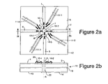
- FIGS. 2 a and 2 b One solution to this problem is shown in FIGS. 2 a and 2 b .
- Switches 10 - 1 through 10 - 4 comprise a set of RF MEMS switches 10 (the numeral 10 when used without a dash and another numeral is used herein to refer to these RF MEMS switches in general as opposed to a particular switch). As will be seen, the number of switches 10 in the set can be greater than four, if desired.
- RF MEMS switches 10 are positioned around common point 7 , preferably in a radial geometry as shown.
- the benefit of this geometry is that each of the selectable ports 1 - 4 sees the same RF environment (including the same impedance) by utilizing the same local geometry which is preferably only varied by rotation about an axis “A” defined through common point 7 . Therefore, each of the ports 1 - 4 should have the same RF performance (or, at least, nearly identical RF performances to each other). Furthermore, since this geometry permits the MEMS devices 10 to be clustered as closely as possible around common point 7 , parasitic reactance should be minimized.
- control line pairs 11 can be arranged at right angles to each other, resulting in very low coupling between them.
- This embodiment has four ports, but, as will be seen, this basic design can be modified to provide a greater (or lesser) number of ports.
- the MEMS switches 10 are preferably disposed in a circular arrangement around central point 7 on substrate 12 .
- the switches 10 lie on a circular arrangement as indicated by the circular line identified by the letter B.
- the switches are preferably arranged equidistantly along the circumference of the circular line identified by the letter B.
- the MEMS switches 10 can be placed individually directly on surface 9 of the circuit board 12 or they may be formed on a small substrate (not shown) as a switch hybrid, which is in turn mounted on surface 9 .
- Via 20 preferably has a pad 8 on the top surface of the printed circuit board 12 to which the MEMS switches 10 can be wired, for example, using ball bonding techniques.
- the switches 10 are also wired to the control lines pairs 11 and to the ports 1 - 4 .
- a common port 7 is fed from the underside of the ground plane through a vertical metal plated via 20 to the top side of the board 12 where it terminates at central point 7 .
- MEMS switches 10 are radially clustered around this central point.
- the centers of the MEMS switches 10 are preferably spaced a common distance (a common radius) away from an axis A of the via 20 . This allows a large number of switches 10 to be fit into a small area, yet allows the coupling between the ports to be minimized.
- the coupling is further minimized by the fact that the RF microstrip lines directed to ports 1 - 4 are disposed at right angles to each other.
- the substrate 12 of this structure preferably is a multi-layer microwave substrate with a buried ground plane 18 .
- the RF microstrip lines coupling to ports 1 - 4 may form the driven elements of an antenna structure, for example, or may be coupled to antenna elements. Such elements may be used for sending and/or receiving RF signals.
- FIGS. 3 a and 3 b show another embodiment of the present invention, in which some of the DC bias lines are implemented as vias 21 which connect with the buried ground plane 18 in substrate 12 .
- the vias 21 may have pads 8 formed on their top surfaces in order to facilitate connecting the ground connections on the MEMS switches 10 thereto. Since each bias line pair 11 consists of a ground line 24 and a signal or control line 23 , each of the ground lines 24 - 1 - 24 - 4 , may be tied to the RF ground plane 18 , with no loss of performance, by means of vias 21 .
- FIG. 4 An additional possible advantage of the geometry of FIGS. 3 a and 3 c is shown in FIG. 4 .
- a feed-through via 20 such as that used for the common port 7 can sometimes have its own parasitic reactance.
- a complementary reactance Z as an external lumped element 25 , one may optimize the RF match of the circuit.
- the reactance Z couples via 20 to ground using one of the vias 21 coupled to ground plane 18 . Since the impedance match is done on the central port 7 , and all other ports are symmetrical, the same matching structure Z will work for all of the ports.
- This lumped element solution is one example of a matching structure, and others will be apparent to those skilled in the art of RF design.
- the ground connections of the MEMS switches 10 are wired to metal plated vias 21 directly or to their associated pads 8 , either of which is in electrical communication with the buried ground plane 18 .
- the via 20 that provides the central RF port passes through a hole or opening 19 in the ground plane 18 , while the vias 21 contact the ground plane 18 .
- the plurality of MEMS switch devices 10 - 1 10 - 4 of FIGS. 3 a , 3 b and 4 are arranged on substrate 12 about a vertical axis A through the substrate, each switch 10 being disposed in a circular arrangement centered on axis A (central point 7 ) with each switch 10 being preferably spaced equidistantly along the circumference of the imaginary circle B defining the circular arrangement.
- the MEMS switches 10 are preferably disposed in a circular arrangement around central point 7 on substrate 12 .
- the switches 10 lie on indicated by the circular line identified by the letter B.
- the switches are preferably arranged equidistantly along the circumference of the circular line identified by the letter B.
- the DC control lines 11 and 22 are depicted as being thinner than are the RF lines 1 - 4 . If the DC lines are much thinner than the RF lines, they will have a higher impedance and coupling with the RF lines will be thereby reduced. While the percentage by which the DC are made thinner than the RF lines is somewhat a matter of tradeoffs, it is believed their width should preferably be about 25% of the width of the RF lines or less. The DC lines should be separated by at least one RF line width from the RF lines to reduce unwanted coupling.
- the MEMS switches may be wired to their RF lines, DC control lines, ground pads or lines by means of wires 30 bonded to the respective switches 10 and their various lines and/or pads.
- both the DC bias switch control lines 23 , 24 associated with each switch 10 are fed through vertical metal plated vias 21 , 26 .
- one of the lines (line 24 ) is grounded by means of via 21 contacting ground plane 18 and the other line (line 23 ) is connected, by means of a via 26 through a hole in the ground plane 18 , to a trace 27 on the back side of the board 12 which functions as a MEMS switch 10 control line.
- all of the DC bias lines 11 pass through metal plated vias 21 , 26 . Half of them contact the ground plane 18 and the other half pass through the ground plane to contact traces 27 on the bottom or back side 13 of the board 12 .
- the RF and DC signals share lines 1 , 2 , 3 , 4 .
- Both the RF and the DC ports of the MEMS switches 10 - 1 . . . 10 - 4 are connected together, as shown in FIG. 6 a .
- the DC portion of the signal may be separated from the RF portion by using an inductor 32 - 1 . . . 32 - 4 in each of the switches' DC circuit.
- This may be either a lumped element, a printed inductor, or an inductive structure such as a very high-impedance RF line.
- Another inductor 34 may be needed to separate the RF signal from the DC ground as shown in FIG. 6 b .
- FIGS. 6 a and 6 b show a four port arrangement, but it is to be understood that this modification would be more apt to be used where space constraints do not allow the other embodiments to be easily utilized.
- the individual switching devices 10 should be connected directly to the central point 7 , which should be a small circle of metal, ideally no larger than is necessary to make proper contact to the via 20 , which is fed from the back side.
- the diameter of the circle B at which the switches are located should preferably be much less than a wavelength for all frequencies in the desired passband of the disclosed single-pole multi-throw switch.
- the radial switching structure described above is combined with a printed antenna structure which may or may not share the same substrate 12 .
- the printed antenna structure 40 preferably includes four conductive cloverleaf elements 36 which define flared notch antennas 37 therebetween.
- the DC bias lines 11 a disposed on the back side of the board, as well as the common RF line 14 , also on the backside of the board, are shown in dashed lines.
- the selectable RF lines on the front side of the board are shown in solid lines.
- the conductive cloverleaf elements are preferably formed on one surface of board 12 using conventional printed circuit board fabrication techniques.
- the cloverleaf elements 36 may be made by appropriately etching a copper-clad printed circuit board, for example.
- the lines on the bottom side (shown dashed) can be similarly made by appropriately etching a copper-clad printed circuit board.
- Each flared notch 37 is fed by a separate microstrip line 1 - 4 , each of which crosses over the notch of an antenna and is shorted to the ground plane 18 (see, e.g., FIG. 5 b ) on the opposite side of board 12 at vias 39 .
- These microstrip lines correspond to the similarly numbered ports 1 - 4 discussed with respect to the switch arrangements of the earlier mentioned figures. RF energy passing down these microstrip lines is radiated from the associated antenna structure in a direction that antenna is pointing (i.e. along the mid-points of the notch of the notch antenna which is excited).
- the DC bias lines 11 and 11 a are preferably routed to a common connector 42 on the bottom side of the board 12 and the RF input preferably comprises a single feed point 41 which is routed to one of the four antenna structures (by means of one of the microstrips 1 - 4 ) as determined by which MEMS switch 10 (see FIG. 5 a the switches 10 are too small to be shown clearly on FIG. 7 , but they are clustered around point 7 ) is closed.
- Bias lines 11 are disposed on the top side of board 12 while bias lines 11 a are disposed on the bottom side thereof. They are coupled together through the board 12 by means of vias. A pad 8 of one via is numbered in FIG.
- FIG. 7 (the other vias are unnumbered due to the limited space available around them for reference numerals, but the vias can, nevertheless, be easily seen).
- the vias in FIG. 7 are shown spaced further from the center point 7 than they would be in an actual embodiment, merely for ease of illustration.
- FIG. 8 An embodiment more complicated than that of FIG. 7 is shown in FIG. 8 .
- This embodiment has eight flared notches 37 defined by cloverleaf elements 36 and a single 1 ⁇ 8 array of RF MEMS switches 10 at the central point 7 (see FIG. 5 a —the switches 10 are again too small to be shown easily on FIG. 8 , but they are nevertheless clustered around central point 7 ).
- This antenna uses the 1 ⁇ 8 MEMS switch to route the common input port to one of eight flared notch antennas 37 .
- This drawing only shows the general concept of the structure and does not show the required DC bias lines or inductors. But those bias lines would be similar to those shown in FIG. 7 , but more numerous given the fact that this embodiment has eight notches 37 rather than four notches 37 .
- FIGS. 7 and 8 demonstrate that the matrix of single-pole, multi-throw MEMS switches can be combined with an antenna structure 40 to create a switched beam diversity antenna of rather inexpensive components.
- the structure shown by FIG. 7 uses four flared notches 37 , which are addressed by a 1 ⁇ 4 MEMS switch matrix preferably arranged in the radial configuration described above.
- FIGS. 3 a and 3 b The preferred embodiment of the hybrid single-pole, multi-throw switch has been described with reference to FIGS. 3 a and 3 b . It is felt that this embodiment can be rather easily manufactured.
- the antenna cloverleaf design of FIG. 8 is preferred since eight slots provide good diversity control.
- FIG. 9 One such solution is shown in FIG. 9 .
- FIG. 9 is not a presently preferred embodiment of this invention, but it is an embodiment that may have sufficient advantages in certain applications, such as when metal plated vias cannot be used, that some practicing the present invention may choose to utilize it. This may be the case when a monolithic approach is taken, when vias and internal ground layers may not be feasible or may not be simple to realize.
- This embodiment builds on the concept that the individual MEMS devices 10 are preferably clustered as closely as possible around a central point 7 to avoid parasitic reactance. This embodiment also recognizes that this may not be possible for a design to have a large number of ports, because when the microstrip transmission lines are brought too close to each other, unwanted coupling occurs.
- a 1 ⁇ 3 switching unit SU is used as a building block for a 1 ⁇ N switch of any desired size.
- Each SU has a pair of MEMS switches 10 for coupling the transmission lines to a central point 7 of the SU.
- Each transmission line port 1 , 2 of a first unit is accessed through a MEMS device 10
- subsequent transmission line ports for example, ports 3 , 4 of a second SU
- third MEMS device(s) 45 which route the RF signals along sections of central transmission line 46 (which may now be of any length required to minimize coupling between ports) to a next 1 ⁇ 3 switching unit SU.
- Each switching unit SU comprises two (or possibly more) MEMS switches 10 clustered around its own central point 7 for coupling the transmission lines thereto and another MEMS switch 45 for passing the incoming signal to yet another switching unit SU.
- two additional (or more) transmission lines may be addressed each through their own individual MEMS device 10 , or the signals may be sent to the next SU through the third MEMS device 45 . Since unused sections of transmission line are switched off when they are not used, they do not present unwanted parasitic reactance. Of course, all of the DC bias methods described in previous embodiments may be applied to this structure as well.
- FIG. 9 thus depicts an alternate design that may be used if a central metal-plated via 20 feature of the earlier embodiments is not feasible.
- the design of FIG. 9 uses a 1 ⁇ 3 switch SU as a building block for a 1 ⁇ N switch of any size. It benefits from the knowledge that dangling sections of RF line will cause parasitic reactance when they are not used.
- the third switch 45 is opened if one of the ports on that unit is selected by means of closing its associated MEMS switch 10 . If neither switch 10 is selected, the third switch 45 is closed, and the signal is routed to the next SU.
- the MEMS switches 10 are preferably disposed in a circular arrangement around central point 7 .
- the switches 10 , 45 also preferably lie on an imaginary circle, here again identified by the letter B.
- the switches 10 , 45 and segment 46 are preferably arranged equidistantly along the circumference identified by the letter B.
- the first portion refers to the element type (a MEMS switch in this case) and the second portion (the 2 in this case) refer to a particular one of those elements (a second MEMS switch 10 in this case).
- This numbering scheme is likely self-explanatory, but it is nevertheless here explained for the reader who might not have previously encountered it.
- the MEM switches 10 - 1 . . . 10 - 4 and 45 may be provided with integral impedance matching elements, such as capacitors, in order to increase the return loss to more than 20 dB. For that reason, the MEM switches disclosed by U.S. Provisional Patent Application Ser. No. 60/470,026 filed May 12, 2003 and entitled “RF MEMS Switch with Integrated Impedance Matching Structure” are believed to be the preferred MEM switches for use in connection with this invention.
Abstract
Description
-
- (1) M. Ando, “Polyhedral Shaped Redundant Coaxial Switch”, U.S. Pat. No. 6,252,473 issued Jun. 26, 2001 and assigned to Hughes Electronics Corporation. This patent describes a waveguide switch using bulk mechanical actuators.
- (2) B. Mayer, “Microwave Switch with Grooves for Isolation of the Passages”, U.S. Pat. No. 6,218,912 issued Apr. 17, 2001 and assigned to Robert Bosch GmbH. This patent describes a waveguide switch with a mechanical rotor structure.
Claims (31)
Priority Applications (1)
| Application Number | Priority Date | Filing Date | Title |
|---|---|---|---|
| US10/714,528 US7276990B2 (en) | 2002-05-15 | 2003-11-14 | Single-pole multi-throw switch having low parasitic reactance, and an antenna incorporating the same |
Applications Claiming Priority (3)
| Application Number | Priority Date | Filing Date | Title |
|---|---|---|---|
| US38109902P | 2002-05-15 | 2002-05-15 | |
| US10/436,753 US7298228B2 (en) | 2002-05-15 | 2003-05-12 | Single-pole multi-throw switch having low parasitic reactance, and an antenna incorporating the same |
| US10/714,528 US7276990B2 (en) | 2002-05-15 | 2003-11-14 | Single-pole multi-throw switch having low parasitic reactance, and an antenna incorporating the same |
Related Parent Applications (1)
| Application Number | Title | Priority Date | Filing Date |
|---|---|---|---|
| US10/436,753 Continuation-In-Part US7298228B2 (en) | 2002-05-15 | 2003-05-12 | Single-pole multi-throw switch having low parasitic reactance, and an antenna incorporating the same |
Publications (2)
| Publication Number | Publication Date |
|---|---|
| US20040135649A1 US20040135649A1 (en) | 2004-07-15 |
| US7276990B2 true US7276990B2 (en) | 2007-10-02 |
Family
ID=29715285
Family Applications (1)
| Application Number | Title | Priority Date | Filing Date |
|---|---|---|---|
| US10/714,528 Expired - Lifetime US7276990B2 (en) | 2002-05-15 | 2003-11-14 | Single-pole multi-throw switch having low parasitic reactance, and an antenna incorporating the same |
Country Status (1)
| Country | Link |
|---|---|
| US (1) | US7276990B2 (en) |
Cited By (168)
| Publication number | Priority date | Publication date | Assignee | Title |
|---|---|---|---|---|
| US20080150830A1 (en) * | 2006-12-22 | 2008-06-26 | Pan Helen K | Multi-band tunable frequency reconfigurable antennas using higher order resonances |
| US8436785B1 (en) | 2010-11-03 | 2013-05-07 | Hrl Laboratories, Llc | Electrically tunable surface impedance structure with suppressed backward wave |
| US8982011B1 (en) | 2011-09-23 | 2015-03-17 | Hrl Laboratories, Llc | Conformal antennas for mitigation of structural blockage |
| US8994609B2 (en) | 2011-09-23 | 2015-03-31 | Hrl Laboratories, Llc | Conformal surface wave feed |
| US20150235771A1 (en) * | 2012-08-10 | 2015-08-20 | Cavendish Kinetics, Inc. | Variable capacitor compromising mems devices for radio frequency applications |
| US9312919B1 (en) | 2014-10-21 | 2016-04-12 | At&T Intellectual Property I, Lp | Transmission device with impairment compensation and methods for use therewith |
| US9461706B1 (en) | 2015-07-31 | 2016-10-04 | At&T Intellectual Property I, Lp | Method and apparatus for exchanging communication signals |
| US9467870B2 (en) | 2013-11-06 | 2016-10-11 | At&T Intellectual Property I, L.P. | Surface-wave communications and methods thereof |
| US9466887B2 (en) | 2010-11-03 | 2016-10-11 | Hrl Laboratories, Llc | Low cost, 2D, electronically-steerable, artificial-impedance-surface antenna |
| US9479266B2 (en) | 2013-12-10 | 2016-10-25 | At&T Intellectual Property I, L.P. | Quasi-optical coupler |
| US9490869B1 (en) | 2015-05-14 | 2016-11-08 | At&T Intellectual Property I, L.P. | Transmission medium having multiple cores and methods for use therewith |
| US9503189B2 (en) | 2014-10-10 | 2016-11-22 | At&T Intellectual Property I, L.P. | Method and apparatus for arranging communication sessions in a communication system |
| US9509415B1 (en) | 2015-06-25 | 2016-11-29 | At&T Intellectual Property I, L.P. | Methods and apparatus for inducing a fundamental wave mode on a transmission medium |
| US9520945B2 (en) | 2014-10-21 | 2016-12-13 | At&T Intellectual Property I, L.P. | Apparatus for providing communication services and methods thereof |
| US9525210B2 (en) | 2014-10-21 | 2016-12-20 | At&T Intellectual Property I, L.P. | Guided-wave transmission device with non-fundamental mode propagation and methods for use therewith |
| US9525524B2 (en) | 2013-05-31 | 2016-12-20 | At&T Intellectual Property I, L.P. | Remote distributed antenna system |
| US9531427B2 (en) | 2014-11-20 | 2016-12-27 | At&T Intellectual Property I, L.P. | Transmission device with mode division multiplexing and methods for use therewith |
| US9564947B2 (en) | 2014-10-21 | 2017-02-07 | At&T Intellectual Property I, L.P. | Guided-wave transmission device with diversity and methods for use therewith |
| US9577307B2 (en) | 2014-10-21 | 2017-02-21 | At&T Intellectual Property I, L.P. | Guided-wave transmission device and methods for use therewith |
| US9608692B2 (en) | 2015-06-11 | 2017-03-28 | At&T Intellectual Property I, L.P. | Repeater and methods for use therewith |
| US9608740B2 (en) | 2015-07-15 | 2017-03-28 | At&T Intellectual Property I, L.P. | Method and apparatus for launching a wave mode that mitigates interference |
| US9615269B2 (en) | 2014-10-02 | 2017-04-04 | At&T Intellectual Property I, L.P. | Method and apparatus that provides fault tolerance in a communication network |
| US9628854B2 (en) | 2014-09-29 | 2017-04-18 | At&T Intellectual Property I, L.P. | Method and apparatus for distributing content in a communication network |
| US9628116B2 (en) | 2015-07-14 | 2017-04-18 | At&T Intellectual Property I, L.P. | Apparatus and methods for transmitting wireless signals |
| US9640850B2 (en) | 2015-06-25 | 2017-05-02 | At&T Intellectual Property I, L.P. | Methods and apparatus for inducing a non-fundamental wave mode on a transmission medium |
| US9654173B2 (en) | 2014-11-20 | 2017-05-16 | At&T Intellectual Property I, L.P. | Apparatus for powering a communication device and methods thereof |
| US9653770B2 (en) | 2014-10-21 | 2017-05-16 | At&T Intellectual Property I, L.P. | Guided wave coupler, coupling module and methods for use therewith |
| US9667317B2 (en) | 2015-06-15 | 2017-05-30 | At&T Intellectual Property I, L.P. | Method and apparatus for providing security using network traffic adjustments |
| US9680670B2 (en) | 2014-11-20 | 2017-06-13 | At&T Intellectual Property I, L.P. | Transmission device with channel equalization and control and methods for use therewith |
| US9685992B2 (en) | 2014-10-03 | 2017-06-20 | At&T Intellectual Property I, L.P. | Circuit panel network and methods thereof |
| US9692101B2 (en) | 2014-08-26 | 2017-06-27 | At&T Intellectual Property I, L.P. | Guided wave couplers for coupling electromagnetic waves between a waveguide surface and a surface of a wire |
| US9699785B2 (en) | 2012-12-05 | 2017-07-04 | At&T Intellectual Property I, L.P. | Backhaul link for distributed antenna system |
| US9705561B2 (en) | 2015-04-24 | 2017-07-11 | At&T Intellectual Property I, L.P. | Directional coupling device and methods for use therewith |
| US9705571B2 (en) | 2015-09-16 | 2017-07-11 | At&T Intellectual Property I, L.P. | Method and apparatus for use with a radio distributed antenna system |
| US9722318B2 (en) | 2015-07-14 | 2017-08-01 | At&T Intellectual Property I, L.P. | Method and apparatus for coupling an antenna to a device |
| US9729197B2 (en) | 2015-10-01 | 2017-08-08 | At&T Intellectual Property I, L.P. | Method and apparatus for communicating network management traffic over a network |
| US9735833B2 (en) | 2015-07-31 | 2017-08-15 | At&T Intellectual Property I, L.P. | Method and apparatus for communications management in a neighborhood network |
| US9742462B2 (en) | 2014-12-04 | 2017-08-22 | At&T Intellectual Property I, L.P. | Transmission medium and communication interfaces and methods for use therewith |
| US9749013B2 (en) | 2015-03-17 | 2017-08-29 | At&T Intellectual Property I, L.P. | Method and apparatus for reducing attenuation of electromagnetic waves guided by a transmission medium |
| US9748626B2 (en) | 2015-05-14 | 2017-08-29 | At&T Intellectual Property I, L.P. | Plurality of cables having different cross-sectional shapes which are bundled together to form a transmission medium |
| US9749053B2 (en) | 2015-07-23 | 2017-08-29 | At&T Intellectual Property I, L.P. | Node device, repeater and methods for use therewith |
| US9755697B2 (en) | 2014-09-15 | 2017-09-05 | At&T Intellectual Property I, L.P. | Method and apparatus for sensing a condition in a transmission medium of electromagnetic waves |
| US9762289B2 (en) | 2014-10-14 | 2017-09-12 | At&T Intellectual Property I, L.P. | Method and apparatus for transmitting or receiving signals in a transportation system |
| US9769128B2 (en) | 2015-09-28 | 2017-09-19 | At&T Intellectual Property I, L.P. | Method and apparatus for encryption of communications over a network |
| US9769020B2 (en) | 2014-10-21 | 2017-09-19 | At&T Intellectual Property I, L.P. | Method and apparatus for responding to events affecting communications in a communication network |
| US9780834B2 (en) | 2014-10-21 | 2017-10-03 | At&T Intellectual Property I, L.P. | Method and apparatus for transmitting electromagnetic waves |
| US9793954B2 (en) | 2015-04-28 | 2017-10-17 | At&T Intellectual Property I, L.P. | Magnetic coupling device and methods for use therewith |
| US9793955B2 (en) | 2015-04-24 | 2017-10-17 | At&T Intellectual Property I, Lp | Passive electrical coupling device and methods for use therewith |
| US9793951B2 (en) | 2015-07-15 | 2017-10-17 | At&T Intellectual Property I, L.P. | Method and apparatus for launching a wave mode that mitigates interference |
| US9800327B2 (en) | 2014-11-20 | 2017-10-24 | At&T Intellectual Property I, L.P. | Apparatus for controlling operations of a communication device and methods thereof |
| US9820146B2 (en) | 2015-06-12 | 2017-11-14 | At&T Intellectual Property I, L.P. | Method and apparatus for authentication and identity management of communicating devices |
| US9838896B1 (en) | 2016-12-09 | 2017-12-05 | At&T Intellectual Property I, L.P. | Method and apparatus for assessing network coverage |
| US9836957B2 (en) | 2015-07-14 | 2017-12-05 | At&T Intellectual Property I, L.P. | Method and apparatus for communicating with premises equipment |
| US9847850B2 (en) | 2014-10-14 | 2017-12-19 | At&T Intellectual Property I, L.P. | Method and apparatus for adjusting a mode of communication in a communication network |
| US9847566B2 (en) | 2015-07-14 | 2017-12-19 | At&T Intellectual Property I, L.P. | Method and apparatus for adjusting a field of a signal to mitigate interference |
| US9853342B2 (en) | 2015-07-14 | 2017-12-26 | At&T Intellectual Property I, L.P. | Dielectric transmission medium connector and methods for use therewith |
| US9860075B1 (en) | 2016-08-26 | 2018-01-02 | At&T Intellectual Property I, L.P. | Method and communication node for broadband distribution |
| US9866309B2 (en) | 2015-06-03 | 2018-01-09 | At&T Intellectual Property I, Lp | Host node device and methods for use therewith |
| US9865911B2 (en) | 2015-06-25 | 2018-01-09 | At&T Intellectual Property I, L.P. | Waveguide system for slot radiating first electromagnetic waves that are combined into a non-fundamental wave mode second electromagnetic wave on a transmission medium |
| US9871283B2 (en) | 2015-07-23 | 2018-01-16 | At&T Intellectual Property I, Lp | Transmission medium having a dielectric core comprised of plural members connected by a ball and socket configuration |
| US9871282B2 (en) | 2015-05-14 | 2018-01-16 | At&T Intellectual Property I, L.P. | At least one transmission medium having a dielectric surface that is covered at least in part by a second dielectric |
| US9876264B2 (en) | 2015-10-02 | 2018-01-23 | At&T Intellectual Property I, Lp | Communication system, guided wave switch and methods for use therewith |
| US9876570B2 (en) | 2015-02-20 | 2018-01-23 | At&T Intellectual Property I, Lp | Guided-wave transmission device with non-fundamental mode propagation and methods for use therewith |
| US9876605B1 (en) | 2016-10-21 | 2018-01-23 | At&T Intellectual Property I, L.P. | Launcher and coupling system to support desired guided wave mode |
| US9882277B2 (en) | 2015-10-02 | 2018-01-30 | At&T Intellectual Property I, Lp | Communication device and antenna assembly with actuated gimbal mount |
| US9882257B2 (en) | 2015-07-14 | 2018-01-30 | At&T Intellectual Property I, L.P. | Method and apparatus for launching a wave mode that mitigates interference |
| US9893795B1 (en) | 2016-12-07 | 2018-02-13 | At&T Intellectual Property I, Lp | Method and repeater for broadband distribution |
| US9904535B2 (en) | 2015-09-14 | 2018-02-27 | At&T Intellectual Property I, L.P. | Method and apparatus for distributing software |
| US9906269B2 (en) | 2014-09-17 | 2018-02-27 | At&T Intellectual Property I, L.P. | Monitoring and mitigating conditions in a communication network |
| US9912027B2 (en) | 2015-07-23 | 2018-03-06 | At&T Intellectual Property I, L.P. | Method and apparatus for exchanging communication signals |
| US9912382B2 (en) | 2015-06-03 | 2018-03-06 | At&T Intellectual Property I, Lp | Network termination and methods for use therewith |
| US9913139B2 (en) | 2015-06-09 | 2018-03-06 | At&T Intellectual Property I, L.P. | Signal fingerprinting for authentication of communicating devices |
| US9911020B1 (en) | 2016-12-08 | 2018-03-06 | At&T Intellectual Property I, L.P. | Method and apparatus for tracking via a radio frequency identification device |
| US9912419B1 (en) | 2016-08-24 | 2018-03-06 | At&T Intellectual Property I, L.P. | Method and apparatus for managing a fault in a distributed antenna system |
| US9917341B2 (en) | 2015-05-27 | 2018-03-13 | At&T Intellectual Property I, L.P. | Apparatus and method for launching electromagnetic waves and for modifying radial dimensions of the propagating electromagnetic waves |
| US9927517B1 (en) | 2016-12-06 | 2018-03-27 | At&T Intellectual Property I, L.P. | Apparatus and methods for sensing rainfall |
| US9948354B2 (en) | 2015-04-28 | 2018-04-17 | At&T Intellectual Property I, L.P. | Magnetic coupling device with reflective plate and methods for use therewith |
| US9948333B2 (en) | 2015-07-23 | 2018-04-17 | At&T Intellectual Property I, L.P. | Method and apparatus for wireless communications to mitigate interference |
| US9954287B2 (en) | 2014-11-20 | 2018-04-24 | At&T Intellectual Property I, L.P. | Apparatus for converting wireless signals and electromagnetic waves and methods thereof |
| US9967173B2 (en) | 2015-07-31 | 2018-05-08 | At&T Intellectual Property I, L.P. | Method and apparatus for authentication and identity management of communicating devices |
| US9973940B1 (en) | 2017-02-27 | 2018-05-15 | At&T Intellectual Property I, L.P. | Apparatus and methods for dynamic impedance matching of a guided wave launcher |
| US9991580B2 (en) | 2016-10-21 | 2018-06-05 | At&T Intellectual Property I, L.P. | Launcher and coupling system for guided wave mode cancellation |
| US9999038B2 (en) | 2013-05-31 | 2018-06-12 | At&T Intellectual Property I, L.P. | Remote distributed antenna system |
| US9997819B2 (en) | 2015-06-09 | 2018-06-12 | At&T Intellectual Property I, L.P. | Transmission medium and method for facilitating propagation of electromagnetic waves via a core |
| US9998870B1 (en) | 2016-12-08 | 2018-06-12 | At&T Intellectual Property I, L.P. | Method and apparatus for proximity sensing |
| US10009065B2 (en) | 2012-12-05 | 2018-06-26 | At&T Intellectual Property I, L.P. | Backhaul link for distributed antenna system |
| US10009067B2 (en) | 2014-12-04 | 2018-06-26 | At&T Intellectual Property I, L.P. | Method and apparatus for configuring a communication interface |
| US10009901B2 (en) | 2015-09-16 | 2018-06-26 | At&T Intellectual Property I, L.P. | Method, apparatus, and computer-readable storage medium for managing utilization of wireless resources between base stations |
| US10009063B2 (en) | 2015-09-16 | 2018-06-26 | At&T Intellectual Property I, L.P. | Method and apparatus for use with a radio distributed antenna system having an out-of-band reference signal |
| US10020587B2 (en) | 2015-07-31 | 2018-07-10 | At&T Intellectual Property I, L.P. | Radial antenna and methods for use therewith |
| US10020844B2 (en) | 2016-12-06 | 2018-07-10 | T&T Intellectual Property I, L.P. | Method and apparatus for broadcast communication via guided waves |
| US10027397B2 (en) | 2016-12-07 | 2018-07-17 | At&T Intellectual Property I, L.P. | Distributed antenna system and methods for use therewith |
| US10033107B2 (en) | 2015-07-14 | 2018-07-24 | At&T Intellectual Property I, L.P. | Method and apparatus for coupling an antenna to a device |
| US10033108B2 (en) | 2015-07-14 | 2018-07-24 | At&T Intellectual Property I, L.P. | Apparatus and methods for generating an electromagnetic wave having a wave mode that mitigates interference |
| US10044409B2 (en) | 2015-07-14 | 2018-08-07 | At&T Intellectual Property I, L.P. | Transmission medium and methods for use therewith |
| US10051629B2 (en) | 2015-09-16 | 2018-08-14 | At&T Intellectual Property I, L.P. | Method and apparatus for use with a radio distributed antenna system having an in-band reference signal |
| US10051483B2 (en) | 2015-10-16 | 2018-08-14 | At&T Intellectual Property I, L.P. | Method and apparatus for directing wireless signals |
| US10069535B2 (en) | 2016-12-08 | 2018-09-04 | At&T Intellectual Property I, L.P. | Apparatus and methods for launching electromagnetic waves having a certain electric field structure |
| US10074890B2 (en) | 2015-10-02 | 2018-09-11 | At&T Intellectual Property I, L.P. | Communication device and antenna with integrated light assembly |
| US10079661B2 (en) | 2015-09-16 | 2018-09-18 | At&T Intellectual Property I, L.P. | Method and apparatus for use with a radio distributed antenna system having a clock reference |
| US10090606B2 (en) | 2015-07-15 | 2018-10-02 | At&T Intellectual Property I, L.P. | Antenna system with dielectric array and methods for use therewith |
| US10090594B2 (en) | 2016-11-23 | 2018-10-02 | At&T Intellectual Property I, L.P. | Antenna system having structural configurations for assembly |
| US10103422B2 (en) | 2016-12-08 | 2018-10-16 | At&T Intellectual Property I, L.P. | Method and apparatus for mounting network devices |
| US10103801B2 (en) | 2015-06-03 | 2018-10-16 | At&T Intellectual Property I, L.P. | Host node device and methods for use therewith |
| US10135145B2 (en) | 2016-12-06 | 2018-11-20 | At&T Intellectual Property I, L.P. | Apparatus and methods for generating an electromagnetic wave along a transmission medium |
| US10135147B2 (en) | 2016-10-18 | 2018-11-20 | At&T Intellectual Property I, L.P. | Apparatus and methods for launching guided waves via an antenna |
| US10136434B2 (en) | 2015-09-16 | 2018-11-20 | At&T Intellectual Property I, L.P. | Method and apparatus for use with a radio distributed antenna system having an ultra-wideband control channel |
| US10135146B2 (en) | 2016-10-18 | 2018-11-20 | At&T Intellectual Property I, L.P. | Apparatus and methods for launching guided waves via circuits |
| US10142086B2 (en) | 2015-06-11 | 2018-11-27 | At&T Intellectual Property I, L.P. | Repeater and methods for use therewith |
| US10139820B2 (en) | 2016-12-07 | 2018-11-27 | At&T Intellectual Property I, L.P. | Method and apparatus for deploying equipment of a communication system |
| US10144036B2 (en) | 2015-01-30 | 2018-12-04 | At&T Intellectual Property I, L.P. | Method and apparatus for mitigating interference affecting a propagation of electromagnetic waves guided by a transmission medium |
| US10148016B2 (en) | 2015-07-14 | 2018-12-04 | At&T Intellectual Property I, L.P. | Apparatus and methods for communicating utilizing an antenna array |
| US10154493B2 (en) | 2015-06-03 | 2018-12-11 | At&T Intellectual Property I, L.P. | Network termination and methods for use therewith |
| US10170840B2 (en) | 2015-07-14 | 2019-01-01 | At&T Intellectual Property I, L.P. | Apparatus and methods for sending or receiving electromagnetic signals |
| US10168695B2 (en) | 2016-12-07 | 2019-01-01 | At&T Intellectual Property I, L.P. | Method and apparatus for controlling an unmanned aircraft |
| US10178445B2 (en) | 2016-11-23 | 2019-01-08 | At&T Intellectual Property I, L.P. | Methods, devices, and systems for load balancing between a plurality of waveguides |
| US10205655B2 (en) | 2015-07-14 | 2019-02-12 | At&T Intellectual Property I, L.P. | Apparatus and methods for communicating utilizing an antenna array and multiple communication paths |
| US10225025B2 (en) | 2016-11-03 | 2019-03-05 | At&T Intellectual Property I, L.P. | Method and apparatus for detecting a fault in a communication system |
| US10224634B2 (en) | 2016-11-03 | 2019-03-05 | At&T Intellectual Property I, L.P. | Methods and apparatus for adjusting an operational characteristic of an antenna |
| US10243270B2 (en) | 2016-12-07 | 2019-03-26 | At&T Intellectual Property I, L.P. | Beam adaptive multi-feed dielectric antenna system and methods for use therewith |
| US10243784B2 (en) | 2014-11-20 | 2019-03-26 | At&T Intellectual Property I, L.P. | System for generating topology information and methods thereof |
| US10264586B2 (en) | 2016-12-09 | 2019-04-16 | At&T Mobility Ii Llc | Cloud-based packet controller and methods for use therewith |
| US10291311B2 (en) | 2016-09-09 | 2019-05-14 | At&T Intellectual Property I, L.P. | Method and apparatus for mitigating a fault in a distributed antenna system |
| US10291334B2 (en) | 2016-11-03 | 2019-05-14 | At&T Intellectual Property I, L.P. | System for detecting a fault in a communication system |
| US10298293B2 (en) | 2017-03-13 | 2019-05-21 | At&T Intellectual Property I, L.P. | Apparatus of communication utilizing wireless network devices |
| US10305190B2 (en) | 2016-12-01 | 2019-05-28 | At&T Intellectual Property I, L.P. | Reflecting dielectric antenna system and methods for use therewith |
| US10312567B2 (en) | 2016-10-26 | 2019-06-04 | At&T Intellectual Property I, L.P. | Launcher with planar strip antenna and methods for use therewith |
| US10320586B2 (en) | 2015-07-14 | 2019-06-11 | At&T Intellectual Property I, L.P. | Apparatus and methods for generating non-interfering electromagnetic waves on an insulated transmission medium |
| US10326689B2 (en) | 2016-12-08 | 2019-06-18 | At&T Intellectual Property I, L.P. | Method and system for providing alternative communication paths |
| US10326494B2 (en) | 2016-12-06 | 2019-06-18 | At&T Intellectual Property I, L.P. | Apparatus for measurement de-embedding and methods for use therewith |
| US10341142B2 (en) | 2015-07-14 | 2019-07-02 | At&T Intellectual Property I, L.P. | Apparatus and methods for generating non-interfering electromagnetic waves on an uninsulated conductor |
| US10340601B2 (en) | 2016-11-23 | 2019-07-02 | At&T Intellectual Property I, L.P. | Multi-antenna system and methods for use therewith |
| US10340983B2 (en) | 2016-12-09 | 2019-07-02 | At&T Intellectual Property I, L.P. | Method and apparatus for surveying remote sites via guided wave communications |
| US10340573B2 (en) | 2016-10-26 | 2019-07-02 | At&T Intellectual Property I, L.P. | Launcher with cylindrical coupling device and methods for use therewith |
| US10340600B2 (en) | 2016-10-18 | 2019-07-02 | At&T Intellectual Property I, L.P. | Apparatus and methods for launching guided waves via plural waveguide systems |
| US10340603B2 (en) | 2016-11-23 | 2019-07-02 | At&T Intellectual Property I, L.P. | Antenna system having shielded structural configurations for assembly |
| US10348391B2 (en) | 2015-06-03 | 2019-07-09 | At&T Intellectual Property I, L.P. | Client node device with frequency conversion and methods for use therewith |
| US10355367B2 (en) | 2015-10-16 | 2019-07-16 | At&T Intellectual Property I, L.P. | Antenna structure for exchanging wireless signals |
| US10359749B2 (en) | 2016-12-07 | 2019-07-23 | At&T Intellectual Property I, L.P. | Method and apparatus for utilities management via guided wave communication |
| US10361489B2 (en) | 2016-12-01 | 2019-07-23 | At&T Intellectual Property I, L.P. | Dielectric dish antenna system and methods for use therewith |
| US10374316B2 (en) | 2016-10-21 | 2019-08-06 | At&T Intellectual Property I, L.P. | System and dielectric antenna with non-uniform dielectric |
| US10382976B2 (en) | 2016-12-06 | 2019-08-13 | At&T Intellectual Property I, L.P. | Method and apparatus for managing wireless communications based on communication paths and network device positions |
| US10389037B2 (en) | 2016-12-08 | 2019-08-20 | At&T Intellectual Property I, L.P. | Apparatus and methods for selecting sections of an antenna array and use therewith |
| US10389029B2 (en) | 2016-12-07 | 2019-08-20 | At&T Intellectual Property I, L.P. | Multi-feed dielectric antenna system with core selection and methods for use therewith |
| US10396887B2 (en) | 2015-06-03 | 2019-08-27 | At&T Intellectual Property I, L.P. | Client node device and methods for use therewith |
| US10411356B2 (en) | 2016-12-08 | 2019-09-10 | At&T Intellectual Property I, L.P. | Apparatus and methods for selectively targeting communication devices with an antenna array |
| US10439675B2 (en) | 2016-12-06 | 2019-10-08 | At&T Intellectual Property I, L.P. | Method and apparatus for repeating guided wave communication signals |
| US10446936B2 (en) | 2016-12-07 | 2019-10-15 | At&T Intellectual Property I, L.P. | Multi-feed dielectric antenna system and methods for use therewith |
| US10498044B2 (en) | 2016-11-03 | 2019-12-03 | At&T Intellectual Property I, L.P. | Apparatus for configuring a surface of an antenna |
| US10530505B2 (en) | 2016-12-08 | 2020-01-07 | At&T Intellectual Property I, L.P. | Apparatus and methods for launching electromagnetic waves along a transmission medium |
| US10535928B2 (en) | 2016-11-23 | 2020-01-14 | At&T Intellectual Property I, L.P. | Antenna system and methods for use therewith |
| US10547348B2 (en) | 2016-12-07 | 2020-01-28 | At&T Intellectual Property I, L.P. | Method and apparatus for switching transmission mediums in a communication system |
| US10601494B2 (en) | 2016-12-08 | 2020-03-24 | At&T Intellectual Property I, L.P. | Dual-band communication device and method for use therewith |
| US10637149B2 (en) | 2016-12-06 | 2020-04-28 | At&T Intellectual Property I, L.P. | Injection molded dielectric antenna and methods for use therewith |
| US10650940B2 (en) | 2015-05-15 | 2020-05-12 | At&T Intellectual Property I, L.P. | Transmission medium having a conductive material and methods for use therewith |
| US10665942B2 (en) | 2015-10-16 | 2020-05-26 | At&T Intellectual Property I, L.P. | Method and apparatus for adjusting wireless communications |
| US10679767B2 (en) | 2015-05-15 | 2020-06-09 | At&T Intellectual Property I, L.P. | Transmission medium having a conductive material and methods for use therewith |
| US10694379B2 (en) | 2016-12-06 | 2020-06-23 | At&T Intellectual Property I, L.P. | Waveguide system with device-based authentication and methods for use therewith |
| US10727599B2 (en) | 2016-12-06 | 2020-07-28 | At&T Intellectual Property I, L.P. | Launcher with slot antenna and methods for use therewith |
| US10755542B2 (en) | 2016-12-06 | 2020-08-25 | At&T Intellectual Property I, L.P. | Method and apparatus for surveillance via guided wave communication |
| US10777873B2 (en) | 2016-12-08 | 2020-09-15 | At&T Intellectual Property I, L.P. | Method and apparatus for mounting network devices |
| US10784670B2 (en) | 2015-07-23 | 2020-09-22 | At&T Intellectual Property I, L.P. | Antenna support for aligning an antenna |
| US10811767B2 (en) | 2016-10-21 | 2020-10-20 | At&T Intellectual Property I, L.P. | System and dielectric antenna with convex dielectric radome |
| US10819035B2 (en) | 2016-12-06 | 2020-10-27 | At&T Intellectual Property I, L.P. | Launcher with helical antenna and methods for use therewith |
| US10916969B2 (en) | 2016-12-08 | 2021-02-09 | At&T Intellectual Property I, L.P. | Method and apparatus for providing power using an inductive coupling |
| US10938108B2 (en) | 2016-12-08 | 2021-03-02 | At&T Intellectual Property I, L.P. | Frequency selective multi-feed dielectric antenna system and methods for use therewith |
| US11032819B2 (en) | 2016-09-15 | 2021-06-08 | At&T Intellectual Property I, L.P. | Method and apparatus for use with a radio distributed antenna system having a control channel reference signal |
| US11399427B2 (en) * | 2019-10-03 | 2022-07-26 | Lockheed Martin Corporation | HMN unit cell class |
Families Citing this family (8)
| Publication number | Priority date | Publication date | Assignee | Title |
|---|---|---|---|---|
| US7298228B2 (en) * | 2002-05-15 | 2007-11-20 | Hrl Laboratories, Llc | Single-pole multi-throw switch having low parasitic reactance, and an antenna incorporating the same |
| US7071888B2 (en) * | 2003-05-12 | 2006-07-04 | Hrl Laboratories, Llc | Steerable leaky wave antenna capable of both forward and backward radiation |
| US7868829B1 (en) | 2008-03-21 | 2011-01-11 | Hrl Laboratories, Llc | Reflectarray |
| US9117610B2 (en) | 2011-11-30 | 2015-08-25 | General Electric Company | Integrated micro-electromechanical switches and a related method thereof |
| CN106532265B (en) * | 2016-11-24 | 2023-04-07 | 南京邮电大学 | Directional reconfigurable microelectronic mechanical antenna and preparation method thereof |
| NL2022186B1 (en) * | 2018-12-12 | 2020-07-02 | Ampleon Netherlands Bv | Power divider |
| CN115349197A (en) * | 2020-05-09 | 2022-11-15 | 华为技术有限公司 | Antenna for a wireless communication device and such a device |
| CN112164625B (en) * | 2020-10-13 | 2022-11-29 | 中北大学 | 4 x 4 full exchange matrix switch based on single-pole four-throw switch |
Citations (99)
| Publication number | Priority date | Publication date | Assignee | Title |
|---|---|---|---|---|
| US3267480A (en) | 1961-02-23 | 1966-08-16 | Hazeltine Research Inc | Polarization converter |
| US3560978A (en) | 1968-11-01 | 1971-02-02 | Itt | Electronically controlled antenna system |
| US3810183A (en) | 1970-12-18 | 1974-05-07 | Ball Brothers Res Corp | Dual slot antenna device |
| US3961333A (en) | 1974-08-29 | 1976-06-01 | Texas Instruments Incorporated | Radome wire grid having low pass frequency characteristics |
| US4045800A (en) | 1975-05-22 | 1977-08-30 | Hughes Aircraft Company | Phase steered subarray antenna |
| US4051477A (en) | 1976-02-17 | 1977-09-27 | Ball Brothers Research Corporation | Wide beam microstrip radiator |
| US4119972A (en) | 1977-02-03 | 1978-10-10 | Nasa | Phased array antenna control |
| US4123759A (en) | 1977-03-21 | 1978-10-31 | Microwave Associates, Inc. | Phased array antenna |
| US4124852A (en) | 1977-01-24 | 1978-11-07 | Raytheon Company | Phased power switching system for scanning antenna array |
| US4127586A (en) | 1970-06-19 | 1978-11-28 | Ciba-Geigy Corporation | Light protection agents |
| US4150382A (en) | 1973-09-13 | 1979-04-17 | Wisconsin Alumni Research Foundation | Non-uniform variable guided wave antennas with electronically controllable scanning |
| US4173759A (en) | 1978-11-06 | 1979-11-06 | Cubic Corporation | Adaptive antenna array and method of operating same |
| US4189733A (en) | 1978-12-08 | 1980-02-19 | Northrop Corporation | Adaptive electronically steerable phased array |
| US4217587A (en) | 1978-08-14 | 1980-08-12 | Westinghouse Electric Corp. | Antenna beam steering controller |
| US4220954A (en) | 1977-12-20 | 1980-09-02 | Marchand Electronic Laboratories, Incorporated | Adaptive antenna system employing FM receiver |
| US4236158A (en) | 1979-03-22 | 1980-11-25 | Motorola, Inc. | Steepest descent controller for an adaptive antenna array |
| US4242685A (en) | 1979-04-27 | 1980-12-30 | Ball Corporation | Slotted cavity antenna |
| US4266203A (en) | 1977-02-25 | 1981-05-05 | Thomson-Csf | Microwave polarization transformer |
| US4308541A (en) | 1979-12-21 | 1981-12-29 | Nasa | Antenna feed system for receiving circular polarization and transmitting linear polarization |
| US4367475A (en) | 1979-10-30 | 1983-01-04 | Ball Corporation | Linearly polarized r.f. radiating slot |
| US4370659A (en) | 1981-07-20 | 1983-01-25 | Sperry Corporation | Antenna |
| US4387377A (en) | 1980-06-24 | 1983-06-07 | Siemens Aktiengesellschaft | Apparatus for converting the polarization of electromagnetic waves |
| US4395713A (en) | 1980-05-06 | 1983-07-26 | Antenna, Incorporated | Transit antenna |
| US4443802A (en) | 1981-04-22 | 1984-04-17 | University Of Illinois Foundation | Stripline fed hybrid slot antenna |
| US4590478A (en) | 1983-06-15 | 1986-05-20 | Sanders Associates, Inc. | Multiple ridge antenna |
| US4594595A (en) | 1984-04-18 | 1986-06-10 | Sanders Associates, Inc. | Circular log-periodic direction-finder array |
| US4672386A (en) | 1984-01-05 | 1987-06-09 | Plessey Overseas Limited | Antenna with radial and edge slot radiators fed with stripline |
| US4684953A (en) | 1984-01-09 | 1987-08-04 | Mcdonnell Douglas Corporation | Reduced height monopole/crossed slot antenna |
| US4700197A (en) | 1984-07-02 | 1987-10-13 | Canadian Patents & Development Ltd. | Adaptive array antenna |
| US4730192A (en) * | 1984-03-23 | 1988-03-08 | International Standard Electric | Monitor for an electronic TACAN beacon |
| US4737795A (en) | 1986-07-25 | 1988-04-12 | General Motors Corporation | Vehicle roof mounted slot antenna with AM and FM grounding |
| US4749966A (en) | 1987-07-01 | 1988-06-07 | The United States Of America As Represented By The Secretary Of The Army | Millimeter wave microstrip circulator |
| US4760402A (en) | 1985-05-30 | 1988-07-26 | Nippondenso Co., Ltd. | Antenna system incorporated in the air spoiler of an automobile |
| US4782346A (en) | 1986-03-11 | 1988-11-01 | General Electric Company | Finline antennas |
| US4803494A (en) | 1987-03-14 | 1989-02-07 | Stc Plc | Wide band antenna |
| US4821040A (en) | 1986-12-23 | 1989-04-11 | Ball Corporation | Circular microstrip vehicular rf antenna |
| US4835541A (en) | 1986-12-29 | 1989-05-30 | Ball Corporation | Near-isotropic low-profile microstrip radiator especially suited for use as a mobile vehicle antenna |
| US4843403A (en) | 1987-07-29 | 1989-06-27 | Ball Corporation | Broadband notch antenna |
| US4843400A (en) | 1988-08-09 | 1989-06-27 | Ford Aerospace Corporation | Aperture coupled circular polarization antenna |
| US4853704A (en) | 1988-05-23 | 1989-08-01 | Ball Corporation | Notch antenna with microstrip feed |
| US4903033A (en) | 1988-04-01 | 1990-02-20 | Ford Aerospace Corporation | Planar dual polarization antenna |
| US4905014A (en) | 1988-04-05 | 1990-02-27 | Malibu Research Associates, Inc. | Microwave phasing structures for electromagnetically emulating reflective surfaces and focusing elements of selected geometry |
| US4916457A (en) | 1988-06-13 | 1990-04-10 | Teledyne Industries, Inc. | Printed-circuit crossed-slot antenna |
| US4922263A (en) | 1986-04-23 | 1990-05-01 | L'etat Francais, Represente Par Le Ministre Des Ptt, Centre National D'etudes Des Telecommunications (Cnet) | Plate antenna with double crossed polarizations |
| US4958165A (en) | 1987-06-09 | 1990-09-18 | Thorm EMI plc | Circular polarization antenna |
| US4975712A (en) | 1989-01-23 | 1990-12-04 | Trw Inc. | Two-dimensional scanning antenna |
| US5021795A (en) | 1989-06-23 | 1991-06-04 | Motorola, Inc. | Passive temperature compensation scheme for microstrip antennas |
| US5023623A (en) | 1989-12-21 | 1991-06-11 | Hughes Aircraft Company | Dual mode antenna apparatus having slotted waveguide and broadband arrays |
| US5070340A (en) | 1989-07-06 | 1991-12-03 | Ball Corporation | Broadband microstrip-fed antenna |
| US5081466A (en) | 1990-05-04 | 1992-01-14 | Motorola, Inc. | Tapered notch antenna |
| US5115217A (en) | 1990-12-06 | 1992-05-19 | California Institute Of Technology | RF tuning element |
| US5146235A (en) | 1989-12-18 | 1992-09-08 | Akg Akustische U. Kino-Gerate Gesellschaft M.B.H. | Helical uhf transmitting and/or receiving antenna |
| US5158611A (en) | 1985-10-28 | 1992-10-27 | Sumitomo Chemical Co., Ltd. | Paper coating composition |
| US5208603A (en) | 1990-06-15 | 1993-05-04 | The Boeing Company | Frequency selective surface (FSS) |
| US5218374A (en) | 1988-09-01 | 1993-06-08 | Apti, Inc. | Power beaming system with printer circuit radiating elements having resonating cavities |
| US5235343A (en) | 1990-08-21 | 1993-08-10 | Societe D'etudes Et De Realisation De Protection Electronique Informatique Electronique | High frequency antenna with a variable directing radiation pattern |
| US5268696A (en) | 1992-04-06 | 1993-12-07 | Westinghouse Electric Corp. | Slotline reflective phase shifting array element utilizing electrostatic switches |
| US5268701A (en) | 1992-03-23 | 1993-12-07 | Raytheon Company | Radio frequency antenna |
| US5278562A (en) | 1992-08-07 | 1994-01-11 | Hughes Missile Systems Company | Method and apparatus using photoresistive materials as switchable EMI barriers and shielding |
| US5287118A (en) | 1990-07-24 | 1994-02-15 | British Aerospace Public Limited Company | Layer frequency selective surface assembly and method of modulating the power or frequency characteristics thereof |
| US5287116A (en) | 1991-05-30 | 1994-02-15 | Kabushiki Kaisha Toshiba | Array antenna generating circularly polarized waves with a plurality of microstrip antennas |
| US5402134A (en) | 1993-03-01 | 1995-03-28 | R. A. Miller Industries, Inc. | Flat plate antenna module |
| US5406292A (en) | 1993-06-09 | 1995-04-11 | Ball Corporation | Crossed-slot antenna having infinite balun feed means |
| US5519408A (en) | 1991-01-22 | 1996-05-21 | Us Air Force | Tapered notch antenna using coplanar waveguide |
| US5525954A (en) | 1993-08-09 | 1996-06-11 | Oki Electric Industry Co., Ltd. | Stripline resonator |
| US5531018A (en) | 1993-12-20 | 1996-07-02 | General Electric Company | Method of micromachining electromagnetically actuated current switches with polyimide reinforcement seals, and switches produced thereby |
| US5532709A (en) | 1994-11-02 | 1996-07-02 | Ford Motor Company | Directional antenna for vehicle entry system |
| US5534877A (en) | 1989-12-14 | 1996-07-09 | Comsat | Orthogonally polarized dual-band printed circuit antenna employing radiating elements capacitively coupled to feedlines |
| US5541614A (en) | 1995-04-04 | 1996-07-30 | Hughes Aircraft Company | Smart antenna system using microelectromechanically tunable dipole antennas and photonic bandgap materials |
| US5557291A (en) | 1995-05-25 | 1996-09-17 | Hughes Aircraft Company | Multiband, phased-array antenna with interleaved tapered-element and waveguide radiators |
| US5581266A (en) | 1993-01-04 | 1996-12-03 | Peng; Sheng Y. | Printed-circuit crossed-slot antenna |
| US5589845A (en) | 1992-12-01 | 1996-12-31 | Superconducting Core Technologies, Inc. | Tuneable electric antenna apparatus including ferroelectric material |
| US5598172A (en) | 1990-11-06 | 1997-01-28 | Thomson - Csf Radant | Dual-polarization microwave lens and its application to a phased-array antenna |
| US5600325A (en) | 1995-06-07 | 1997-02-04 | Hughes Electronics | Ferro-electric frequency selective surface radome |
| US5611940A (en) | 1994-04-28 | 1997-03-18 | Siemens Aktiengesellschaft | Microsystem with integrated circuit and micromechanical component, and production process |
| US5619366A (en) | 1992-06-08 | 1997-04-08 | Texas Instruments Incorporated | Controllable surface filter |
| US5621571A (en) | 1994-02-14 | 1997-04-15 | Minnesota Mining And Manufacturing Company | Integrated retroreflective electronic display |
| US5638946A (en) | 1996-01-11 | 1997-06-17 | Northeastern University | Micromechanical switch with insulated switch contact |
| US5644319A (en) | 1995-05-31 | 1997-07-01 | Industrial Technology Research Institute | Multi-resonance horizontal-U shaped antenna |
| US5694134A (en) | 1992-12-01 | 1997-12-02 | Superconducting Core Technologies, Inc. | Phased array antenna system including a coplanar waveguide feed arrangement |
| US5767807A (en) | 1996-06-05 | 1998-06-16 | International Business Machines Corporation | Communication system and methods utilizing a reactively controlled directive array |
| US5808527A (en) | 1996-12-21 | 1998-09-15 | Hughes Electronics Corporation | Tunable microwave network using microelectromechanical switches |
| US5874915A (en) | 1997-08-08 | 1999-02-23 | Raytheon Company | Wideband cylindrical UHF array |
| US5892485A (en) | 1997-02-25 | 1999-04-06 | Pacific Antenna Technologies | Dual frequency reflector antenna feed element |
| US5894288A (en) | 1997-08-08 | 1999-04-13 | Raytheon Company | Wideband end-fire array |
| US5905465A (en) | 1997-04-23 | 1999-05-18 | Ball Aerospace & Technologies Corp. | Antenna system |
| US5923303A (en) | 1997-12-24 | 1999-07-13 | U S West, Inc. | Combined space and polarization diversity antennas |
| US5926139A (en) | 1997-07-02 | 1999-07-20 | Lucent Technologies Inc. | Planar dual frequency band antenna |
| US5929819A (en) | 1996-12-17 | 1999-07-27 | Hughes Electronics Corporation | Flat antenna for satellite communication |
| US5943016A (en) | 1995-12-07 | 1999-08-24 | Atlantic Aerospace Electronics, Corp. | Tunable microstrip patch antenna and feed network therefor |
| US5945951A (en) | 1997-09-03 | 1999-08-31 | Andrew Corporation | High isolation dual polarized antenna system with microstrip-fed aperture coupled patches |
| US5949382A (en) | 1990-09-28 | 1999-09-07 | Raytheon Company | Dielectric flare notch radiator with separate transmit and receive ports |
| US5966096A (en) | 1996-04-24 | 1999-10-12 | France Telecom | Compact printed antenna for radiation at low elevation |
| US5966101A (en) | 1997-05-09 | 1999-10-12 | Motorola, Inc. | Multi-layered compact slot antenna structure and method |
| US6005519A (en) | 1996-09-04 | 1999-12-21 | 3 Com Corporation | Tunable microstrip antenna and method for tuning the same |
| US6005521A (en) | 1996-04-25 | 1999-12-21 | Kyocera Corporation | Composite antenna |
| US6008770A (en) | 1996-06-24 | 1999-12-28 | Ricoh Company, Ltd. | Planar antenna and antenna array |
| US6016125A (en) | 1996-08-29 | 2000-01-18 | Telefonaktiebolaget Lm Ericsson | Antenna device and method for portable radio equipment |
| US6337668B1 (en) * | 1999-03-05 | 2002-01-08 | Matsushita Electric Industrial Co., Ltd. | Antenna apparatus |
Family Cites Families (41)
| Publication number | Priority date | Publication date | Assignee | Title |
|---|---|---|---|---|
| US6061025A (en) * | 1995-12-07 | 2000-05-09 | Atlantic Aerospace Electronics Corporation | Tunable microstrip patch antenna and control system therefor |
| KR980010984A (en) * | 1996-07-02 | 1998-04-30 | 구자홍 | How to implement white balance of plasma display |
| JP3684285B2 (en) * | 1997-03-10 | 2005-08-17 | 株式会社日立製作所 | Tunable slot antenna |
| KR100312364B1 (en) * | 1997-05-30 | 2001-12-28 | 가나이 쓰도무 | Tunable slot antenna |
| EP0996992A1 (en) * | 1997-07-09 | 2000-05-03 | Allgon AB | Trap microstrip pifa |
| US6046655A (en) * | 1997-11-10 | 2000-04-04 | Datron/Transco Inc. | Antenna feed system |
| US6040803A (en) * | 1998-02-19 | 2000-03-21 | Ericsson Inc. | Dual band diversity antenna having parasitic radiating element |
| US6054659A (en) * | 1998-03-09 | 2000-04-25 | General Motors Corporation | Integrated electrostatically-actuated micromachined all-metal micro-relays |
| DE19817573A1 (en) * | 1998-04-20 | 1999-10-21 | Heinz Lindenmeier | Antenna for multiple radio services |
| US6081235A (en) * | 1998-04-30 | 2000-06-27 | The United States Of America As Represented By The Administrator Of The National Aeronautics And Space Administration | High resolution scanning reflectarray antenna |
| US6046659A (en) * | 1998-05-15 | 2000-04-04 | Hughes Electronics Corporation | Design and fabrication of broadband surface-micromachined micro-electro-mechanical switches for microwave and millimeter-wave applications |
| DE19822072C1 (en) * | 1998-05-16 | 2000-01-13 | Bosch Gmbh Robert | Microwave switch, e.g. for satellite application as redundant switch, achieves higher operating frequency with a significantly greater gap between the rotor and generator housing |
| JP2000036702A (en) * | 1998-07-21 | 2000-02-02 | Hitachi Ltd | Radio terminal |
| US6037905A (en) * | 1998-08-06 | 2000-03-14 | The United States Of America As Represented By The Secretary Of The Army | Azimuth steerable antenna |
| US6175723B1 (en) * | 1998-08-12 | 2001-01-16 | Board Of Trustees Operating Michigan State University | Self-structuring antenna system with a switchable antenna array and an optimizing controller |
| US6081239A (en) * | 1998-10-23 | 2000-06-27 | Gradient Technologies, Llc | Planar antenna including a superstrate lens having an effective dielectric constant |
| US6246377B1 (en) * | 1998-11-02 | 2001-06-12 | Fantasma Networks, Inc. | Antenna comprising two separate wideband notch regions on one coplanar substrate |
| US6075485A (en) * | 1998-11-03 | 2000-06-13 | Atlantic Aerospace Electronics Corp. | Reduced weight artificial dielectric antennas and method for providing the same |
| US6252473B1 (en) * | 1999-01-06 | 2001-06-26 | Hughes Electronics Corporation | Polyhedral-shaped redundant coaxial switch |
| US6191724B1 (en) * | 1999-01-28 | 2001-02-20 | Mcewan Thomas E. | Short pulse microwave transceiver |
| JP3672770B2 (en) * | 1999-07-08 | 2005-07-20 | 株式会社国際電気通信基礎技術研究所 | Array antenna device |
| US6175337B1 (en) * | 1999-09-17 | 2001-01-16 | The United States Of America As Represented By The Secretary Of The Army | High-gain, dielectric loaded, slotted waveguide antenna |
| US6198438B1 (en) * | 1999-10-04 | 2001-03-06 | The United States Of America As Represented By The Secretary Of The Air Force | Reconfigurable microstrip antenna array geometry which utilizes micro-electro-mechanical system (MEMS) switches |
| SE0002617D0 (en) * | 1999-10-29 | 2000-07-11 | Allgon Ab | An antenna device for transmitting and / or receiving RF waves |
| US6366254B1 (en) * | 2000-03-15 | 2002-04-02 | Hrl Laboratories, Llc | Planar antenna with switched beam diversity for interference reduction in a mobile environment |
| US6518931B1 (en) * | 2000-03-15 | 2003-02-11 | Hrl Laboratories, Llc | Vivaldi cloverleaf antenna |
| WO2001071935A1 (en) * | 2000-03-17 | 2001-09-27 | Bae Systems Information And Electronic Systems Integration, Inc. | Reconfigurable diplexer for communications applications |
| US6552696B1 (en) * | 2000-03-29 | 2003-04-22 | Hrl Laboratories, Llc | Electronically tunable reflector |
| US6538621B1 (en) * | 2000-03-29 | 2003-03-25 | Hrl Laboratories, Llc | Tunable impedance surface |
| US6404401B2 (en) * | 2000-04-28 | 2002-06-11 | Bae Systems Information And Electronic Systems Integration Inc. | Metamorphic parallel plate antenna |
| US6204819B1 (en) * | 2000-05-22 | 2001-03-20 | Telefonaktiebolaget L.M. Ericsson | Convertible loop/inverted-f antennas and wireless communicators incorporating the same |
| TW483190B (en) * | 2000-06-02 | 2002-04-11 | Ind Tech Res Inst | Broadband microstrip leaky wave antenna and its feeding system |
| US6741207B1 (en) * | 2000-06-30 | 2004-05-25 | Raytheon Company | Multi-bit phase shifters using MEM RF switches |
| US20020036586A1 (en) * | 2000-09-22 | 2002-03-28 | Tantivy Communications, Inc. | Adaptive antenna for use in wireless communication systems |
| US6515635B2 (en) * | 2000-09-22 | 2003-02-04 | Tantivy Communications, Inc. | Adaptive antenna for use in wireless communication systems |
| US6388631B1 (en) * | 2001-03-19 | 2002-05-14 | Hrl Laboratories Llc | Reconfigurable interleaved phased array antenna |
| US6525695B2 (en) * | 2001-04-30 | 2003-02-25 | E-Tenna Corporation | Reconfigurable artificial magnetic conductor using voltage controlled capacitors with coplanar resistive biasing network |
| US6864848B2 (en) * | 2001-12-27 | 2005-03-08 | Hrl Laboratories, Llc | RF MEMs-tuned slot antenna and a method of making same |
| TW549620U (en) * | 2002-11-13 | 2003-08-21 | Hon Hai Prec Ind Co Ltd | Multi-band antenna |
| US6940363B2 (en) * | 2002-12-17 | 2005-09-06 | Intel Corporation | Switch architecture using MEMS switches and solid state switches in parallel |
| US7002517B2 (en) * | 2003-06-20 | 2006-02-21 | Anritsu Company | Fixed-frequency beam-steerable leaky-wave microstrip antenna |
-
2003
- 2003-11-14 US US10/714,528 patent/US7276990B2/en not_active Expired - Lifetime
Patent Citations (101)
| Publication number | Priority date | Publication date | Assignee | Title |
|---|---|---|---|---|
| US3267480A (en) | 1961-02-23 | 1966-08-16 | Hazeltine Research Inc | Polarization converter |
| US3560978A (en) | 1968-11-01 | 1971-02-02 | Itt | Electronically controlled antenna system |
| US4127586A (en) | 1970-06-19 | 1978-11-28 | Ciba-Geigy Corporation | Light protection agents |
| US3810183A (en) | 1970-12-18 | 1974-05-07 | Ball Brothers Res Corp | Dual slot antenna device |
| US4150382A (en) | 1973-09-13 | 1979-04-17 | Wisconsin Alumni Research Foundation | Non-uniform variable guided wave antennas with electronically controllable scanning |
| US3961333A (en) | 1974-08-29 | 1976-06-01 | Texas Instruments Incorporated | Radome wire grid having low pass frequency characteristics |
| US4045800A (en) | 1975-05-22 | 1977-08-30 | Hughes Aircraft Company | Phase steered subarray antenna |
| US4051477A (en) | 1976-02-17 | 1977-09-27 | Ball Brothers Research Corporation | Wide beam microstrip radiator |
| US4124852A (en) | 1977-01-24 | 1978-11-07 | Raytheon Company | Phased power switching system for scanning antenna array |
| US4119972A (en) | 1977-02-03 | 1978-10-10 | Nasa | Phased array antenna control |
| US4266203A (en) | 1977-02-25 | 1981-05-05 | Thomson-Csf | Microwave polarization transformer |
| US4123759A (en) | 1977-03-21 | 1978-10-31 | Microwave Associates, Inc. | Phased array antenna |
| US4220954A (en) | 1977-12-20 | 1980-09-02 | Marchand Electronic Laboratories, Incorporated | Adaptive antenna system employing FM receiver |
| US4217587A (en) | 1978-08-14 | 1980-08-12 | Westinghouse Electric Corp. | Antenna beam steering controller |
| US4173759A (en) | 1978-11-06 | 1979-11-06 | Cubic Corporation | Adaptive antenna array and method of operating same |
| US4189733A (en) | 1978-12-08 | 1980-02-19 | Northrop Corporation | Adaptive electronically steerable phased array |
| US4236158A (en) | 1979-03-22 | 1980-11-25 | Motorola, Inc. | Steepest descent controller for an adaptive antenna array |
| US4242685A (en) | 1979-04-27 | 1980-12-30 | Ball Corporation | Slotted cavity antenna |
| US4367475A (en) | 1979-10-30 | 1983-01-04 | Ball Corporation | Linearly polarized r.f. radiating slot |
| US4308541A (en) | 1979-12-21 | 1981-12-29 | Nasa | Antenna feed system for receiving circular polarization and transmitting linear polarization |
| US4395713A (en) | 1980-05-06 | 1983-07-26 | Antenna, Incorporated | Transit antenna |
| US4387377A (en) | 1980-06-24 | 1983-06-07 | Siemens Aktiengesellschaft | Apparatus for converting the polarization of electromagnetic waves |
| US4443802A (en) | 1981-04-22 | 1984-04-17 | University Of Illinois Foundation | Stripline fed hybrid slot antenna |
| US4370659A (en) | 1981-07-20 | 1983-01-25 | Sperry Corporation | Antenna |
| US4590478A (en) | 1983-06-15 | 1986-05-20 | Sanders Associates, Inc. | Multiple ridge antenna |
| US4672386A (en) | 1984-01-05 | 1987-06-09 | Plessey Overseas Limited | Antenna with radial and edge slot radiators fed with stripline |
| US4684953A (en) | 1984-01-09 | 1987-08-04 | Mcdonnell Douglas Corporation | Reduced height monopole/crossed slot antenna |
| US4730192A (en) * | 1984-03-23 | 1988-03-08 | International Standard Electric | Monitor for an electronic TACAN beacon |
| US4594595A (en) | 1984-04-18 | 1986-06-10 | Sanders Associates, Inc. | Circular log-periodic direction-finder array |
| US4700197A (en) | 1984-07-02 | 1987-10-13 | Canadian Patents & Development Ltd. | Adaptive array antenna |
| US4760402A (en) | 1985-05-30 | 1988-07-26 | Nippondenso Co., Ltd. | Antenna system incorporated in the air spoiler of an automobile |
| US5158611A (en) | 1985-10-28 | 1992-10-27 | Sumitomo Chemical Co., Ltd. | Paper coating composition |
| US4782346A (en) | 1986-03-11 | 1988-11-01 | General Electric Company | Finline antennas |
| US4922263A (en) | 1986-04-23 | 1990-05-01 | L'etat Francais, Represente Par Le Ministre Des Ptt, Centre National D'etudes Des Telecommunications (Cnet) | Plate antenna with double crossed polarizations |
| US4737795A (en) | 1986-07-25 | 1988-04-12 | General Motors Corporation | Vehicle roof mounted slot antenna with AM and FM grounding |
| US4821040A (en) | 1986-12-23 | 1989-04-11 | Ball Corporation | Circular microstrip vehicular rf antenna |
| US4835541A (en) | 1986-12-29 | 1989-05-30 | Ball Corporation | Near-isotropic low-profile microstrip radiator especially suited for use as a mobile vehicle antenna |
| US4803494A (en) | 1987-03-14 | 1989-02-07 | Stc Plc | Wide band antenna |
| US4958165A (en) | 1987-06-09 | 1990-09-18 | Thorm EMI plc | Circular polarization antenna |
| US4749966A (en) | 1987-07-01 | 1988-06-07 | The United States Of America As Represented By The Secretary Of The Army | Millimeter wave microstrip circulator |
| US4843403A (en) | 1987-07-29 | 1989-06-27 | Ball Corporation | Broadband notch antenna |
| US4903033A (en) | 1988-04-01 | 1990-02-20 | Ford Aerospace Corporation | Planar dual polarization antenna |
| US4905014A (en) | 1988-04-05 | 1990-02-27 | Malibu Research Associates, Inc. | Microwave phasing structures for electromagnetically emulating reflective surfaces and focusing elements of selected geometry |
| US4853704A (en) | 1988-05-23 | 1989-08-01 | Ball Corporation | Notch antenna with microstrip feed |
| US4916457A (en) | 1988-06-13 | 1990-04-10 | Teledyne Industries, Inc. | Printed-circuit crossed-slot antenna |
| US4843400A (en) | 1988-08-09 | 1989-06-27 | Ford Aerospace Corporation | Aperture coupled circular polarization antenna |
| US5218374A (en) | 1988-09-01 | 1993-06-08 | Apti, Inc. | Power beaming system with printer circuit radiating elements having resonating cavities |
| US4975712A (en) | 1989-01-23 | 1990-12-04 | Trw Inc. | Two-dimensional scanning antenna |
| US5021795A (en) | 1989-06-23 | 1991-06-04 | Motorola, Inc. | Passive temperature compensation scheme for microstrip antennas |
| US5070340A (en) | 1989-07-06 | 1991-12-03 | Ball Corporation | Broadband microstrip-fed antenna |
| US5534877A (en) | 1989-12-14 | 1996-07-09 | Comsat | Orthogonally polarized dual-band printed circuit antenna employing radiating elements capacitively coupled to feedlines |
| US5146235A (en) | 1989-12-18 | 1992-09-08 | Akg Akustische U. Kino-Gerate Gesellschaft M.B.H. | Helical uhf transmitting and/or receiving antenna |
| US5023623A (en) | 1989-12-21 | 1991-06-11 | Hughes Aircraft Company | Dual mode antenna apparatus having slotted waveguide and broadband arrays |
| US5081466A (en) | 1990-05-04 | 1992-01-14 | Motorola, Inc. | Tapered notch antenna |
| US5208603A (en) | 1990-06-15 | 1993-05-04 | The Boeing Company | Frequency selective surface (FSS) |
| US5287118A (en) | 1990-07-24 | 1994-02-15 | British Aerospace Public Limited Company | Layer frequency selective surface assembly and method of modulating the power or frequency characteristics thereof |
| US5235343A (en) | 1990-08-21 | 1993-08-10 | Societe D'etudes Et De Realisation De Protection Electronique Informatique Electronique | High frequency antenna with a variable directing radiation pattern |
| US5949382A (en) | 1990-09-28 | 1999-09-07 | Raytheon Company | Dielectric flare notch radiator with separate transmit and receive ports |
| US5598172A (en) | 1990-11-06 | 1997-01-28 | Thomson - Csf Radant | Dual-polarization microwave lens and its application to a phased-array antenna |
| US5115217A (en) | 1990-12-06 | 1992-05-19 | California Institute Of Technology | RF tuning element |
| US5519408A (en) | 1991-01-22 | 1996-05-21 | Us Air Force | Tapered notch antenna using coplanar waveguide |
| US5287116A (en) | 1991-05-30 | 1994-02-15 | Kabushiki Kaisha Toshiba | Array antenna generating circularly polarized waves with a plurality of microstrip antennas |
| US5268701A (en) | 1992-03-23 | 1993-12-07 | Raytheon Company | Radio frequency antenna |
| US5268696A (en) | 1992-04-06 | 1993-12-07 | Westinghouse Electric Corp. | Slotline reflective phase shifting array element utilizing electrostatic switches |
| US5619365A (en) | 1992-06-08 | 1997-04-08 | Texas Instruments Incorporated | Elecronically tunable optical periodic surface filters with an alterable resonant frequency |
| US5619366A (en) | 1992-06-08 | 1997-04-08 | Texas Instruments Incorporated | Controllable surface filter |
| US5278562A (en) | 1992-08-07 | 1994-01-11 | Hughes Missile Systems Company | Method and apparatus using photoresistive materials as switchable EMI barriers and shielding |
| US5694134A (en) | 1992-12-01 | 1997-12-02 | Superconducting Core Technologies, Inc. | Phased array antenna system including a coplanar waveguide feed arrangement |
| US5721194A (en) | 1992-12-01 | 1998-02-24 | Superconducting Core Technologies, Inc. | Tuneable microwave devices including fringe effect capacitor incorporating ferroelectric films |
| US5589845A (en) | 1992-12-01 | 1996-12-31 | Superconducting Core Technologies, Inc. | Tuneable electric antenna apparatus including ferroelectric material |
| US5581266A (en) | 1993-01-04 | 1996-12-03 | Peng; Sheng Y. | Printed-circuit crossed-slot antenna |
| US5402134A (en) | 1993-03-01 | 1995-03-28 | R. A. Miller Industries, Inc. | Flat plate antenna module |
| US5406292A (en) | 1993-06-09 | 1995-04-11 | Ball Corporation | Crossed-slot antenna having infinite balun feed means |
| US5525954A (en) | 1993-08-09 | 1996-06-11 | Oki Electric Industry Co., Ltd. | Stripline resonator |
| US5531018A (en) | 1993-12-20 | 1996-07-02 | General Electric Company | Method of micromachining electromagnetically actuated current switches with polyimide reinforcement seals, and switches produced thereby |
| US5621571A (en) | 1994-02-14 | 1997-04-15 | Minnesota Mining And Manufacturing Company | Integrated retroreflective electronic display |
| US5611940A (en) | 1994-04-28 | 1997-03-18 | Siemens Aktiengesellschaft | Microsystem with integrated circuit and micromechanical component, and production process |
| US5532709A (en) | 1994-11-02 | 1996-07-02 | Ford Motor Company | Directional antenna for vehicle entry system |
| US5541614A (en) | 1995-04-04 | 1996-07-30 | Hughes Aircraft Company | Smart antenna system using microelectromechanically tunable dipole antennas and photonic bandgap materials |
| US5557291A (en) | 1995-05-25 | 1996-09-17 | Hughes Aircraft Company | Multiband, phased-array antenna with interleaved tapered-element and waveguide radiators |
| US5644319A (en) | 1995-05-31 | 1997-07-01 | Industrial Technology Research Institute | Multi-resonance horizontal-U shaped antenna |
| US5600325A (en) | 1995-06-07 | 1997-02-04 | Hughes Electronics | Ferro-electric frequency selective surface radome |
| US5943016A (en) | 1995-12-07 | 1999-08-24 | Atlantic Aerospace Electronics, Corp. | Tunable microstrip patch antenna and feed network therefor |
| US5638946A (en) | 1996-01-11 | 1997-06-17 | Northeastern University | Micromechanical switch with insulated switch contact |
| US5966096A (en) | 1996-04-24 | 1999-10-12 | France Telecom | Compact printed antenna for radiation at low elevation |
| US6005521A (en) | 1996-04-25 | 1999-12-21 | Kyocera Corporation | Composite antenna |
| US5767807A (en) | 1996-06-05 | 1998-06-16 | International Business Machines Corporation | Communication system and methods utilizing a reactively controlled directive array |
| US6008770A (en) | 1996-06-24 | 1999-12-28 | Ricoh Company, Ltd. | Planar antenna and antenna array |
| US6016125A (en) | 1996-08-29 | 2000-01-18 | Telefonaktiebolaget Lm Ericsson | Antenna device and method for portable radio equipment |
| US6005519A (en) | 1996-09-04 | 1999-12-21 | 3 Com Corporation | Tunable microstrip antenna and method for tuning the same |
| US5929819A (en) | 1996-12-17 | 1999-07-27 | Hughes Electronics Corporation | Flat antenna for satellite communication |
| US5808527A (en) | 1996-12-21 | 1998-09-15 | Hughes Electronics Corporation | Tunable microwave network using microelectromechanical switches |
| US5892485A (en) | 1997-02-25 | 1999-04-06 | Pacific Antenna Technologies | Dual frequency reflector antenna feed element |
| US5905465A (en) | 1997-04-23 | 1999-05-18 | Ball Aerospace & Technologies Corp. | Antenna system |
| US5966101A (en) | 1997-05-09 | 1999-10-12 | Motorola, Inc. | Multi-layered compact slot antenna structure and method |
| US5926139A (en) | 1997-07-02 | 1999-07-20 | Lucent Technologies Inc. | Planar dual frequency band antenna |
| US5894288A (en) | 1997-08-08 | 1999-04-13 | Raytheon Company | Wideband end-fire array |
| US5874915A (en) | 1997-08-08 | 1999-02-23 | Raytheon Company | Wideband cylindrical UHF array |
| US5945951A (en) | 1997-09-03 | 1999-08-31 | Andrew Corporation | High isolation dual polarized antenna system with microstrip-fed aperture coupled patches |
| US5923303A (en) | 1997-12-24 | 1999-07-13 | U S West, Inc. | Combined space and polarization diversity antennas |
| US6337668B1 (en) * | 1999-03-05 | 2002-01-08 | Matsushita Electric Industrial Co., Ltd. | Antenna apparatus |
Non-Patent Citations (60)
| Title |
|---|
| Balanis, C., "Aperture Antennas," Antenna Theory, Analysis and Design, 2nd Edition, Ch. 12, pp. 575-597 (1997). |
| Balanis, C., "Microstrip Antennas," Antenna Theory, Analysis and Design, 2nd Edition, Ch. 14, pp. 722-736 (1997). |
| Bialkowski, M.E., et al., "Electronically Steered Antenna System for the Australian Mobilesat," IEE Proc.-Microw. Antennas Propag.,, vol. 143, No. 4, pp. 347-352 (Aug. 1996). |
| Bradley, T.W., et al., "Development Of A Voltage-Variable Dielectric (VVD), Electronic Scan Antenna," Radar 97, Publication No. 449, pp. 383-385 (Oct. 1997). |
| Brown, W.C., "The History of Power Transmission by Radio Waves," IEEE Transactions on Microwave Theory and Techniques, vol. MTT-32, No. 9, pp. 1230-1242 (Sep. 1984). |
| Bushbeck, M.D., et al., "a Tunable Switcher Dielectric Grating," IEEE Microwave and Guided Wave Letters, vol. 3, No. 9, pp. 296-298 (Sep. 1993). |
| Chambers, B., et al., "Tunable Radar Absorbers Using Frequency Selective Surfaces," 11th International Conference on Antennas and Propagation, vol. 50, pp. 832-835, 2001. |
| Chang, T.K., et al., "Frequency Selective Surfaces on Biased Ferrite Substrates," Electronics Letters, vol. 30, No. 15, pp. 1193-1194 (Jul. 21, 1994). |
| Chen, P.W., et al., Planar Double-Layer Leaky Wave Microstrip Antenna, IEEE Transactions on Antennas and Propagation, vol. 50, pp. 832-835 (2002). |
| Chen, Q., et al., "FDTD diakoptic design of a slop-loop antenna excited by a coplanar waveguide," Proceedings of the 25th European Microwave Conference 1995, vol. 2, Conf. 25, pp. 815-819 (Sep. 4, 1995). |
| Cognard, J., "Alignment of Nematic Liquid Crystals and Their Mixtures," Mol. Cryst. Liq., Cryst. Suppl. 1, pp. 1-74 (1982). |
| Doane, J.W., et al., "Field Controlled Light Scattering from Nematic Microdroplets," Appl. Phys. Lett., vol. 48, pp. 269-271 (Jan. 1986). |
| Ellis, T.J., et al., "MM-Wave Tapered Slot Antennas on Micromachined Photonic Bandgap Dielectrics," 1996 IEEE MTT-S International Microwave Symposium Digest, vol. 2, 1157-1160 (1996). |
| Fay, P., et al., "High-Performance Antimonide-Based Heterostructure Backward Diodes for Millimeter-Wave Detection," IEEE Electron Device Letters, vol. 23, No. 10, pp. 585-587 (Oct. 2002). |
| Gianvittorio, J.P., et al., "Reconfigurable MEMS-enabled Frequency Selective Surfaces," Electronic Letters, vol. 38, No. 25, pp. 1627-1628 (Dec. 5, 2002). |
| Gold, S.H., et al., "Review of High-Power Microwave Source Research," Rev. Sci. Instrum., vol. 68, No. 11, pp. 3945-3974 (Nov. 1997). |
| Grbic, A., et al., "Experimental Verification of Backward Wave Radiation From A Negative Refractive Index Metamaterial," Journal of Applied Physics, vol. 92, No. 10, pp. 5930-5935 (Nov. 15, 2002). |
| Hu, C.N., et al., "Analysis and Design of Large Leaky-Mode Array Employing The Coupled-Mode Approach," IEEE Transactions on Microwave Theory and Techniques, vol. 49, No. 4, pp. 629-636 (Apr. 2001). |
| Jablonski, W., et al., "Microwave Schottky Diode With Beam-Lead Contacts," 13th Conference on Microwaves, Radar and Wireless Communications, MIKON-2000, vol. 2, pp. 678-681 (2000). |
| Jensen, M.A., et al., "EM Interaction of Handset Antennas and a Human in Personal Communications," Proceedings of the IEEE, vol. 83, No. 1, pp. 7-17 (Jan. 1995). |
| Jensen, M.A., et al., "Performance Analysis of Antennas for Hand-held Transceivers Using FDTD," IEEE Transactions on Antennas and Propagation, vol. 42, No. 8, pp. 1106-1113 (Aug. 1994). |
| Koert, P., et al., "Millimeter Wave Technology for Space Power Beaming," IEEE Transactions on Microwave Theory and Techniques, vol. 40, No. 6, pp. 1251-1258 (Jun. 1992). |
| Lee, J.W., et al., "TM-Wave Reduction From Grooves In A Dielectric-Covered Ground Plane," IEEE Transactions on Antennas and Propagation, vol. 49, No. 1, pp. 104-105 (Jan. 2001). |
| Lezec, H.J., et al., "Beaming Light from a Subwavelength Aperture," Science, vol. 297, pp. 820-821 (Aug. 2, 2002). |
| Lima, A.C., et al., "Tunable Frequency Selective Surfaces Using Liquid Substrates," Electronic Letters, vol. 30, No. 4, pp. 281-282 (Feb. 17, 1994). |
| Linardou, I., et al., "Twin Vivaldi Antenna Fed By Coplanar Waveguide," Electronics Letters, vol. 33, No. 22, pp. 1835-1837 (1997). |
| Malherbe, A., et al., "The Compenasation of Step Discontiues in TEM-Mode Transmission Lines," IEEE Transactions on Microwave Theory and Techniques, vol. MTT-26, No. 11, pp. 883-885 (Nov. 1978). |
| Maruhashi, K., et al., "Design and Performance of a Ka-Band Monolithic Phase Shifter Utilizing Nonresonant FET Switches," IEEE Transactions on Microwave Theory and Techniques, vol. 48, No. 8, pp. 1313-1317 (Aug. 2000). |
| McSpadden, J.O.,et al., "Design and Experiments of a High-Conversion-Efficiency 5.8-GHz Rectenna," IEEE Transactions on Microwave Theory and Techniques, vol. 46, No. 12, pp. 2053-2060 (Dec. 1998). |
| Oak, A.C., et al. "A Varactor Tuned 16 Element MESFET Grid Oscillator," Antennas and Propagation Society International Symposium. pp. 1296-1299 (1995). |
| Perini, P., et al., "Angle and Space Diversity Comparisons in Different Mobile Radio Environments," IEEE Transactions on Antennas and Propagation, vol. 46, No. 6, pp. 764-775 (Jun. 1998). |
| Ramo, S., et al., Fields and Waves in Communication Electronics, 3rd Edition, Sections 9.8-9.11, pp. 476-487 (1994). |
| Rebeiz, G.M., et al., "RF MEMS Switches and Switch Circuits," IEEE Microwave Magazine, pp. 59-71 (Dec. 2001). |
| Schaffner, J., et al., "Reconfigurable Aperture Antennas Using RF MEMS Switches for Multi-Octave Tunability and Beam Steering," IEEE Antennas and Propagation Society International Symposium, 2000 Digest, vol. 1 of 4, pp. 321-324 (Jul. 16, 2000). |
| Schulman, J.N., et al., "Sb-Heterostructure Interband Backward Diodes," IEEE Electron Device Letters, vol. 21, No. 7, pp. 353-355 (Jul. 2000). |
| Semouchkina, E., et al., "Numerical Modeling and Experimental Study of A Novel Leaky Wave Antenna," Antennas and Propagation Society, IEEE International Symposium, vol. 4, pp. 234-237 (2001). |
| Sievenpiper, D., et al., "Beam Steering Microwve Reflector Based On Electrically Tunable Impedance Surface," Electronics Letters, vol. 38, No. 21, pp. 1237-1238 (Oct. 1, 2002). |
| Sievenpiper, D., et al., "Eliminating Surface Currents With Metallodielectric Photonic Crystals," 1998 MTT-S International Microwave Symposium Digest, vol. 2, pp. 663-666 (Jun. 7, 1998). |
| Sievenpiper, D., et al., "High-Impedance Electromagnetic Surfaces with a Forbidden Frequency Band," IEEE Transactions on Microwave Theory and Techniques, vol. 47, No. 11, pp. 2059-2074 (Nov. 1999). |
| Sievenpiper, D., et al., "High-Impedance Electromagnetic Surfaces," Ph. D. Dissertation, Dept. Of Electrical Engineering, University of California, Los Angeles, CA, pp. i-xi, 1-150 (1999). |
| Sievenpiper, D., et al., "Low-Profile, Four Sector Diversity Antenna On High-Impedance Ground Plane," Electronics Letters, vol. 36, No. 16, pp. 1343-1345 (Aug. 3, 2000). |
| Sievenpiper, D.F., et al., "Two-Dimensional Beam Steering Using an Electrically Tunable Impedance Surface," IEEE Transactions on Antennas and Propagation, vol. 51, No. 10, pp. 2713-2722 (Oct. 2003). |
| Sor, J., et al., "A Reconfigurable Leaky-Wave/Patch Microstrip Aperture For Phased-Array Applications," IEEE Transactions on Microwave Theory and Techniques, vol. 50, No. 8, pp. 1877-1884 (Aug. 2002). |
| Strasser, B., et al., "5.8-GHz Circularly Polarized Rectifying Antenna for Wireless Microwave Power Transmission," IEEE Transactions on Microwave Theory and Techniques, vol. 50, No. 8, pp. 1870-1876 (Aug. 2002). |
| Swartz, N., "Ready for CMDA 2000 1xEV-Do?," Wireless Review, 2 pages total (Oct. 29, 2001). |
| Swartz, Nikki, Ready for CDMA2000 1xEV-DO, Oct. 2001, Wireless Review, 2 pages. * |
| U.S. Appl. No. 10/786,736, filed Nov. 2004, Shaffner et al. |
| U.S. Appl. No. 10/792,411, filed Nov. 2004, Sievenpiper. |
| U.S. Appl. No. 10/792,412, filed Nov. 2004, Sievenpiper. |
| U.S. Appl. No. 10/836,966, filed Nov. 2004, Sievenpiper. |
| U.S. Appl. No. 10/844,104, filed Dec. 2004, Sievenpiper. |
| U.S. Appl. No. 10/944,032, filed Sep. 17, 2004, Sievenpiper. |
| Vaughan , R., "Spaced Directive Antennas for Mobile Comminications by the Fourier Transform Method," IEEE Transactions on Antennas and Propagation, vol. 48, No. 7, pp. 1025-1032 (Jul. 2000). |
| Vaughan, Mark J., et al., "InP-Based 28 Gh<SUB>z </SUB>Integrated Antennas for Point-to-Multipoint Distribution," Proceedings of the IEEE/Cornell Conference on Advanced Concepts in High Speed Semiconductor Devices and Circuits, pp. 75-84 (1995). |
| Wang, C.J., et al., "Two-Dimensional Scanning Leaky Wave Antenna by Utilizing the Phased Array," IEEE Microwave and Wireless Components Letters, vol. 12, No. 8, pp. 311-313, (Aug. 2002). |
| Wu, S.T., et al., "High Birefringence and Wide Nematic Range Bis-Tolane Liquid Crystals," Appl. Phys. Lett., vol. 74, No. 5, pp. 344-346 (Jan. 18, 1999). |
| Yang, F.R., et al., "A Uniplanar Compact Photonic-Bandgap (UC-PBG) Structure and its Applications for Microwave Circuits," IEEE Transactions on Microwave Theory and Techniques, vol. 47, No. 8, pp. 1509-1514 (Aug. 1999). |
| Yang, Hung-Yu David, et al., "Theory of Line-Source Radiation From A Metal-Strip Grating Dielectric-Slab Structure," IEEE Transactions on Antennas and Propagation, vol. 48, No. 4, pp. 556-564 (2000). |
| Yashchyshyn, Y., et al., "The Leaky-Wave Antenna With Ferroelectric Substrate," 14th International Conference on Microwaves, Radar and Wireless Communications, MIKON-2002, vol. 2, pp. 218-221 (2002). |
| Yashchyshyn, Y., et al., The Leaky-Wave Antenna With Ferroelectric Substrate, 14th International Conference on Microwaves, Radar and Wireless Communications, MIKON-2002, vol. 2, pp. 218-221 (2002). |
Cited By (226)
| Publication number | Priority date | Publication date | Assignee | Title |
|---|---|---|---|---|
| US8369796B2 (en) * | 2006-12-22 | 2013-02-05 | Intel Corporation | Multi-band tunable frequency reconfigurable antennas using higher order resonances |
| US20080150830A1 (en) * | 2006-12-22 | 2008-06-26 | Pan Helen K | Multi-band tunable frequency reconfigurable antennas using higher order resonances |
| US9466887B2 (en) | 2010-11-03 | 2016-10-11 | Hrl Laboratories, Llc | Low cost, 2D, electronically-steerable, artificial-impedance-surface antenna |
| US8436785B1 (en) | 2010-11-03 | 2013-05-07 | Hrl Laboratories, Llc | Electrically tunable surface impedance structure with suppressed backward wave |
| US8982011B1 (en) | 2011-09-23 | 2015-03-17 | Hrl Laboratories, Llc | Conformal antennas for mitigation of structural blockage |
| US8994609B2 (en) | 2011-09-23 | 2015-03-31 | Hrl Laboratories, Llc | Conformal surface wave feed |
| US20150235771A1 (en) * | 2012-08-10 | 2015-08-20 | Cavendish Kinetics, Inc. | Variable capacitor compromising mems devices for radio frequency applications |
| US9443658B2 (en) * | 2012-08-10 | 2016-09-13 | Cavendish Kinetics, Inc. | Variable capacitor compromising MEMS devices for radio frequency applications |
| US9699785B2 (en) | 2012-12-05 | 2017-07-04 | At&T Intellectual Property I, L.P. | Backhaul link for distributed antenna system |
| US9788326B2 (en) | 2012-12-05 | 2017-10-10 | At&T Intellectual Property I, L.P. | Backhaul link for distributed antenna system |
| US10194437B2 (en) | 2012-12-05 | 2019-01-29 | At&T Intellectual Property I, L.P. | Backhaul link for distributed antenna system |
| US10009065B2 (en) | 2012-12-05 | 2018-06-26 | At&T Intellectual Property I, L.P. | Backhaul link for distributed antenna system |
| US9525524B2 (en) | 2013-05-31 | 2016-12-20 | At&T Intellectual Property I, L.P. | Remote distributed antenna system |
| US9930668B2 (en) | 2013-05-31 | 2018-03-27 | At&T Intellectual Property I, L.P. | Remote distributed antenna system |
| US10091787B2 (en) | 2013-05-31 | 2018-10-02 | At&T Intellectual Property I, L.P. | Remote distributed antenna system |
| US9999038B2 (en) | 2013-05-31 | 2018-06-12 | At&T Intellectual Property I, L.P. | Remote distributed antenna system |
| US10051630B2 (en) | 2013-05-31 | 2018-08-14 | At&T Intellectual Property I, L.P. | Remote distributed antenna system |
| US9467870B2 (en) | 2013-11-06 | 2016-10-11 | At&T Intellectual Property I, L.P. | Surface-wave communications and methods thereof |
| US9674711B2 (en) | 2013-11-06 | 2017-06-06 | At&T Intellectual Property I, L.P. | Surface-wave communications and methods thereof |
| US9661505B2 (en) | 2013-11-06 | 2017-05-23 | At&T Intellectual Property I, L.P. | Surface-wave communications and methods thereof |
| US9794003B2 (en) | 2013-12-10 | 2017-10-17 | At&T Intellectual Property I, L.P. | Quasi-optical coupler |
| US9479266B2 (en) | 2013-12-10 | 2016-10-25 | At&T Intellectual Property I, L.P. | Quasi-optical coupler |
| US9876584B2 (en) | 2013-12-10 | 2018-01-23 | At&T Intellectual Property I, L.P. | Quasi-optical coupler |
| US10096881B2 (en) | 2014-08-26 | 2018-10-09 | At&T Intellectual Property I, L.P. | Guided wave couplers for coupling electromagnetic waves to an outer surface of a transmission medium |
| US9692101B2 (en) | 2014-08-26 | 2017-06-27 | At&T Intellectual Property I, L.P. | Guided wave couplers for coupling electromagnetic waves between a waveguide surface and a surface of a wire |
| US9755697B2 (en) | 2014-09-15 | 2017-09-05 | At&T Intellectual Property I, L.P. | Method and apparatus for sensing a condition in a transmission medium of electromagnetic waves |
| US9768833B2 (en) | 2014-09-15 | 2017-09-19 | At&T Intellectual Property I, L.P. | Method and apparatus for sensing a condition in a transmission medium of electromagnetic waves |
| US9906269B2 (en) | 2014-09-17 | 2018-02-27 | At&T Intellectual Property I, L.P. | Monitoring and mitigating conditions in a communication network |
| US10063280B2 (en) | 2014-09-17 | 2018-08-28 | At&T Intellectual Property I, L.P. | Monitoring and mitigating conditions in a communication network |
| US9628854B2 (en) | 2014-09-29 | 2017-04-18 | At&T Intellectual Property I, L.P. | Method and apparatus for distributing content in a communication network |
| US9615269B2 (en) | 2014-10-02 | 2017-04-04 | At&T Intellectual Property I, L.P. | Method and apparatus that provides fault tolerance in a communication network |
| US9973416B2 (en) | 2014-10-02 | 2018-05-15 | At&T Intellectual Property I, L.P. | Method and apparatus that provides fault tolerance in a communication network |
| US9998932B2 (en) | 2014-10-02 | 2018-06-12 | At&T Intellectual Property I, L.P. | Method and apparatus that provides fault tolerance in a communication network |
| US9685992B2 (en) | 2014-10-03 | 2017-06-20 | At&T Intellectual Property I, L.P. | Circuit panel network and methods thereof |
| US9866276B2 (en) | 2014-10-10 | 2018-01-09 | At&T Intellectual Property I, L.P. | Method and apparatus for arranging communication sessions in a communication system |
| US9503189B2 (en) | 2014-10-10 | 2016-11-22 | At&T Intellectual Property I, L.P. | Method and apparatus for arranging communication sessions in a communication system |
| US9847850B2 (en) | 2014-10-14 | 2017-12-19 | At&T Intellectual Property I, L.P. | Method and apparatus for adjusting a mode of communication in a communication network |
| US9762289B2 (en) | 2014-10-14 | 2017-09-12 | At&T Intellectual Property I, L.P. | Method and apparatus for transmitting or receiving signals in a transportation system |
| US9973299B2 (en) | 2014-10-14 | 2018-05-15 | At&T Intellectual Property I, L.P. | Method and apparatus for adjusting a mode of communication in a communication network |
| US9954286B2 (en) | 2014-10-21 | 2018-04-24 | At&T Intellectual Property I, L.P. | Guided-wave transmission device with non-fundamental mode propagation and methods for use therewith |
| US9525210B2 (en) | 2014-10-21 | 2016-12-20 | At&T Intellectual Property I, L.P. | Guided-wave transmission device with non-fundamental mode propagation and methods for use therewith |
| US9312919B1 (en) | 2014-10-21 | 2016-04-12 | At&T Intellectual Property I, Lp | Transmission device with impairment compensation and methods for use therewith |
| US9577307B2 (en) | 2014-10-21 | 2017-02-21 | At&T Intellectual Property I, L.P. | Guided-wave transmission device and methods for use therewith |
| US9705610B2 (en) | 2014-10-21 | 2017-07-11 | At&T Intellectual Property I, L.P. | Transmission device with impairment compensation and methods for use therewith |
| US9871558B2 (en) | 2014-10-21 | 2018-01-16 | At&T Intellectual Property I, L.P. | Guided-wave transmission device and methods for use therewith |
| US9948355B2 (en) | 2014-10-21 | 2018-04-17 | At&T Intellectual Property I, L.P. | Apparatus for providing communication services and methods thereof |
| US9571209B2 (en) | 2014-10-21 | 2017-02-14 | At&T Intellectual Property I, L.P. | Transmission device with impairment compensation and methods for use therewith |
| US9577306B2 (en) | 2014-10-21 | 2017-02-21 | At&T Intellectual Property I, L.P. | Guided-wave transmission device and methods for use therewith |
| US9564947B2 (en) | 2014-10-21 | 2017-02-07 | At&T Intellectual Property I, L.P. | Guided-wave transmission device with diversity and methods for use therewith |
| US9876587B2 (en) | 2014-10-21 | 2018-01-23 | At&T Intellectual Property I, L.P. | Transmission device with impairment compensation and methods for use therewith |
| US9520945B2 (en) | 2014-10-21 | 2016-12-13 | At&T Intellectual Property I, L.P. | Apparatus for providing communication services and methods thereof |
| US9960808B2 (en) | 2014-10-21 | 2018-05-01 | At&T Intellectual Property I, L.P. | Guided-wave transmission device and methods for use therewith |
| US9912033B2 (en) | 2014-10-21 | 2018-03-06 | At&T Intellectual Property I, Lp | Guided wave coupler, coupling module and methods for use therewith |
| US9780834B2 (en) | 2014-10-21 | 2017-10-03 | At&T Intellectual Property I, L.P. | Method and apparatus for transmitting electromagnetic waves |
| US9627768B2 (en) | 2014-10-21 | 2017-04-18 | At&T Intellectual Property I, L.P. | Guided-wave transmission device with non-fundamental mode propagation and methods for use therewith |
| US9653770B2 (en) | 2014-10-21 | 2017-05-16 | At&T Intellectual Property I, L.P. | Guided wave coupler, coupling module and methods for use therewith |
| US9596001B2 (en) | 2014-10-21 | 2017-03-14 | At&T Intellectual Property I, L.P. | Apparatus for providing communication services and methods thereof |
| US9769020B2 (en) | 2014-10-21 | 2017-09-19 | At&T Intellectual Property I, L.P. | Method and apparatus for responding to events affecting communications in a communication network |
| US9654173B2 (en) | 2014-11-20 | 2017-05-16 | At&T Intellectual Property I, L.P. | Apparatus for powering a communication device and methods thereof |
| US9749083B2 (en) | 2014-11-20 | 2017-08-29 | At&T Intellectual Property I, L.P. | Transmission device with mode division multiplexing and methods for use therewith |
| US9531427B2 (en) | 2014-11-20 | 2016-12-27 | At&T Intellectual Property I, L.P. | Transmission device with mode division multiplexing and methods for use therewith |
| US9680670B2 (en) | 2014-11-20 | 2017-06-13 | At&T Intellectual Property I, L.P. | Transmission device with channel equalization and control and methods for use therewith |
| US9544006B2 (en) | 2014-11-20 | 2017-01-10 | At&T Intellectual Property I, L.P. | Transmission device with mode division multiplexing and methods for use therewith |
| US10243784B2 (en) | 2014-11-20 | 2019-03-26 | At&T Intellectual Property I, L.P. | System for generating topology information and methods thereof |
| US9742521B2 (en) | 2014-11-20 | 2017-08-22 | At&T Intellectual Property I, L.P. | Transmission device with mode division multiplexing and methods for use therewith |
| US9712350B2 (en) | 2014-11-20 | 2017-07-18 | At&T Intellectual Property I, L.P. | Transmission device with channel equalization and control and methods for use therewith |
| US9800327B2 (en) | 2014-11-20 | 2017-10-24 | At&T Intellectual Property I, L.P. | Apparatus for controlling operations of a communication device and methods thereof |
| US9954287B2 (en) | 2014-11-20 | 2018-04-24 | At&T Intellectual Property I, L.P. | Apparatus for converting wireless signals and electromagnetic waves and methods thereof |
| US10009067B2 (en) | 2014-12-04 | 2018-06-26 | At&T Intellectual Property I, L.P. | Method and apparatus for configuring a communication interface |
| US9742462B2 (en) | 2014-12-04 | 2017-08-22 | At&T Intellectual Property I, L.P. | Transmission medium and communication interfaces and methods for use therewith |
| US10144036B2 (en) | 2015-01-30 | 2018-12-04 | At&T Intellectual Property I, L.P. | Method and apparatus for mitigating interference affecting a propagation of electromagnetic waves guided by a transmission medium |
| US9876570B2 (en) | 2015-02-20 | 2018-01-23 | At&T Intellectual Property I, Lp | Guided-wave transmission device with non-fundamental mode propagation and methods for use therewith |
| US9876571B2 (en) | 2015-02-20 | 2018-01-23 | At&T Intellectual Property I, Lp | Guided-wave transmission device with non-fundamental mode propagation and methods for use therewith |
| US9749013B2 (en) | 2015-03-17 | 2017-08-29 | At&T Intellectual Property I, L.P. | Method and apparatus for reducing attenuation of electromagnetic waves guided by a transmission medium |
| US10224981B2 (en) | 2015-04-24 | 2019-03-05 | At&T Intellectual Property I, Lp | Passive electrical coupling device and methods for use therewith |
| US9705561B2 (en) | 2015-04-24 | 2017-07-11 | At&T Intellectual Property I, L.P. | Directional coupling device and methods for use therewith |
| US9831912B2 (en) | 2015-04-24 | 2017-11-28 | At&T Intellectual Property I, Lp | Directional coupling device and methods for use therewith |
| US9793955B2 (en) | 2015-04-24 | 2017-10-17 | At&T Intellectual Property I, Lp | Passive electrical coupling device and methods for use therewith |
| US9948354B2 (en) | 2015-04-28 | 2018-04-17 | At&T Intellectual Property I, L.P. | Magnetic coupling device with reflective plate and methods for use therewith |
| US9793954B2 (en) | 2015-04-28 | 2017-10-17 | At&T Intellectual Property I, L.P. | Magnetic coupling device and methods for use therewith |
| US9748626B2 (en) | 2015-05-14 | 2017-08-29 | At&T Intellectual Property I, L.P. | Plurality of cables having different cross-sectional shapes which are bundled together to form a transmission medium |
| US9490869B1 (en) | 2015-05-14 | 2016-11-08 | At&T Intellectual Property I, L.P. | Transmission medium having multiple cores and methods for use therewith |
| US9887447B2 (en) | 2015-05-14 | 2018-02-06 | At&T Intellectual Property I, L.P. | Transmission medium having multiple cores and methods for use therewith |
| US9871282B2 (en) | 2015-05-14 | 2018-01-16 | At&T Intellectual Property I, L.P. | At least one transmission medium having a dielectric surface that is covered at least in part by a second dielectric |
| US10679767B2 (en) | 2015-05-15 | 2020-06-09 | At&T Intellectual Property I, L.P. | Transmission medium having a conductive material and methods for use therewith |
| US10650940B2 (en) | 2015-05-15 | 2020-05-12 | At&T Intellectual Property I, L.P. | Transmission medium having a conductive material and methods for use therewith |
| US9917341B2 (en) | 2015-05-27 | 2018-03-13 | At&T Intellectual Property I, L.P. | Apparatus and method for launching electromagnetic waves and for modifying radial dimensions of the propagating electromagnetic waves |
| US9866309B2 (en) | 2015-06-03 | 2018-01-09 | At&T Intellectual Property I, Lp | Host node device and methods for use therewith |
| US9912381B2 (en) | 2015-06-03 | 2018-03-06 | At&T Intellectual Property I, Lp | Network termination and methods for use therewith |
| US10154493B2 (en) | 2015-06-03 | 2018-12-11 | At&T Intellectual Property I, L.P. | Network termination and methods for use therewith |
| US9967002B2 (en) | 2015-06-03 | 2018-05-08 | At&T Intellectual I, Lp | Network termination and methods for use therewith |
| US10797781B2 (en) | 2015-06-03 | 2020-10-06 | At&T Intellectual Property I, L.P. | Client node device and methods for use therewith |
| US10812174B2 (en) | 2015-06-03 | 2020-10-20 | At&T Intellectual Property I, L.P. | Client node device and methods for use therewith |
| US10103801B2 (en) | 2015-06-03 | 2018-10-16 | At&T Intellectual Property I, L.P. | Host node device and methods for use therewith |
| US9935703B2 (en) | 2015-06-03 | 2018-04-03 | At&T Intellectual Property I, L.P. | Host node device and methods for use therewith |
| US10348391B2 (en) | 2015-06-03 | 2019-07-09 | At&T Intellectual Property I, L.P. | Client node device with frequency conversion and methods for use therewith |
| US10396887B2 (en) | 2015-06-03 | 2019-08-27 | At&T Intellectual Property I, L.P. | Client node device and methods for use therewith |
| US9912382B2 (en) | 2015-06-03 | 2018-03-06 | At&T Intellectual Property I, Lp | Network termination and methods for use therewith |
| US10050697B2 (en) | 2015-06-03 | 2018-08-14 | At&T Intellectual Property I, L.P. | Host node device and methods for use therewith |
| US9997819B2 (en) | 2015-06-09 | 2018-06-12 | At&T Intellectual Property I, L.P. | Transmission medium and method for facilitating propagation of electromagnetic waves via a core |
| US9913139B2 (en) | 2015-06-09 | 2018-03-06 | At&T Intellectual Property I, L.P. | Signal fingerprinting for authentication of communicating devices |
| US10027398B2 (en) | 2015-06-11 | 2018-07-17 | At&T Intellectual Property I, Lp | Repeater and methods for use therewith |
| US10142086B2 (en) | 2015-06-11 | 2018-11-27 | At&T Intellectual Property I, L.P. | Repeater and methods for use therewith |
| US10142010B2 (en) | 2015-06-11 | 2018-11-27 | At&T Intellectual Property I, L.P. | Repeater and methods for use therewith |
| US9608692B2 (en) | 2015-06-11 | 2017-03-28 | At&T Intellectual Property I, L.P. | Repeater and methods for use therewith |
| US9820146B2 (en) | 2015-06-12 | 2017-11-14 | At&T Intellectual Property I, L.P. | Method and apparatus for authentication and identity management of communicating devices |
| US9667317B2 (en) | 2015-06-15 | 2017-05-30 | At&T Intellectual Property I, L.P. | Method and apparatus for providing security using network traffic adjustments |
| US10069185B2 (en) | 2015-06-25 | 2018-09-04 | At&T Intellectual Property I, L.P. | Methods and apparatus for inducing a non-fundamental wave mode on a transmission medium |
| US9640850B2 (en) | 2015-06-25 | 2017-05-02 | At&T Intellectual Property I, L.P. | Methods and apparatus for inducing a non-fundamental wave mode on a transmission medium |
| US9787412B2 (en) | 2015-06-25 | 2017-10-10 | At&T Intellectual Property I, L.P. | Methods and apparatus for inducing a fundamental wave mode on a transmission medium |
| US9882657B2 (en) | 2015-06-25 | 2018-01-30 | At&T Intellectual Property I, L.P. | Methods and apparatus for inducing a fundamental wave mode on a transmission medium |
| US9509415B1 (en) | 2015-06-25 | 2016-11-29 | At&T Intellectual Property I, L.P. | Methods and apparatus for inducing a fundamental wave mode on a transmission medium |
| US9865911B2 (en) | 2015-06-25 | 2018-01-09 | At&T Intellectual Property I, L.P. | Waveguide system for slot radiating first electromagnetic waves that are combined into a non-fundamental wave mode second electromagnetic wave on a transmission medium |
| US10090601B2 (en) | 2015-06-25 | 2018-10-02 | At&T Intellectual Property I, L.P. | Waveguide system and methods for inducing a non-fundamental wave mode on a transmission medium |
| US10033107B2 (en) | 2015-07-14 | 2018-07-24 | At&T Intellectual Property I, L.P. | Method and apparatus for coupling an antenna to a device |
| US10170840B2 (en) | 2015-07-14 | 2019-01-01 | At&T Intellectual Property I, L.P. | Apparatus and methods for sending or receiving electromagnetic signals |
| US9836957B2 (en) | 2015-07-14 | 2017-12-05 | At&T Intellectual Property I, L.P. | Method and apparatus for communicating with premises equipment |
| US10148016B2 (en) | 2015-07-14 | 2018-12-04 | At&T Intellectual Property I, L.P. | Apparatus and methods for communicating utilizing an antenna array |
| US9853342B2 (en) | 2015-07-14 | 2017-12-26 | At&T Intellectual Property I, L.P. | Dielectric transmission medium connector and methods for use therewith |
| US9929755B2 (en) | 2015-07-14 | 2018-03-27 | At&T Intellectual Property I, L.P. | Method and apparatus for coupling an antenna to a device |
| US9722318B2 (en) | 2015-07-14 | 2017-08-01 | At&T Intellectual Property I, L.P. | Method and apparatus for coupling an antenna to a device |
| US10044409B2 (en) | 2015-07-14 | 2018-08-07 | At&T Intellectual Property I, L.P. | Transmission medium and methods for use therewith |
| US10341142B2 (en) | 2015-07-14 | 2019-07-02 | At&T Intellectual Property I, L.P. | Apparatus and methods for generating non-interfering electromagnetic waves on an uninsulated conductor |
| US9882257B2 (en) | 2015-07-14 | 2018-01-30 | At&T Intellectual Property I, L.P. | Method and apparatus for launching a wave mode that mitigates interference |
| US9947982B2 (en) | 2015-07-14 | 2018-04-17 | At&T Intellectual Property I, Lp | Dielectric transmission medium connector and methods for use therewith |
| US9847566B2 (en) | 2015-07-14 | 2017-12-19 | At&T Intellectual Property I, L.P. | Method and apparatus for adjusting a field of a signal to mitigate interference |
| US10205655B2 (en) | 2015-07-14 | 2019-02-12 | At&T Intellectual Property I, L.P. | Apparatus and methods for communicating utilizing an antenna array and multiple communication paths |
| US10033108B2 (en) | 2015-07-14 | 2018-07-24 | At&T Intellectual Property I, L.P. | Apparatus and methods for generating an electromagnetic wave having a wave mode that mitigates interference |
| US9628116B2 (en) | 2015-07-14 | 2017-04-18 | At&T Intellectual Property I, L.P. | Apparatus and methods for transmitting wireless signals |
| US10320586B2 (en) | 2015-07-14 | 2019-06-11 | At&T Intellectual Property I, L.P. | Apparatus and methods for generating non-interfering electromagnetic waves on an insulated transmission medium |
| US10090606B2 (en) | 2015-07-15 | 2018-10-02 | At&T Intellectual Property I, L.P. | Antenna system with dielectric array and methods for use therewith |
| US9793951B2 (en) | 2015-07-15 | 2017-10-17 | At&T Intellectual Property I, L.P. | Method and apparatus for launching a wave mode that mitigates interference |
| US9608740B2 (en) | 2015-07-15 | 2017-03-28 | At&T Intellectual Property I, L.P. | Method and apparatus for launching a wave mode that mitigates interference |
| US9912027B2 (en) | 2015-07-23 | 2018-03-06 | At&T Intellectual Property I, L.P. | Method and apparatus for exchanging communication signals |
| US10784670B2 (en) | 2015-07-23 | 2020-09-22 | At&T Intellectual Property I, L.P. | Antenna support for aligning an antenna |
| US9948333B2 (en) | 2015-07-23 | 2018-04-17 | At&T Intellectual Property I, L.P. | Method and apparatus for wireless communications to mitigate interference |
| US9806818B2 (en) | 2015-07-23 | 2017-10-31 | At&T Intellectual Property I, Lp | Node device, repeater and methods for use therewith |
| US10074886B2 (en) | 2015-07-23 | 2018-09-11 | At&T Intellectual Property I, L.P. | Dielectric transmission medium comprising a plurality of rigid dielectric members coupled together in a ball and socket configuration |
| US9749053B2 (en) | 2015-07-23 | 2017-08-29 | At&T Intellectual Property I, L.P. | Node device, repeater and methods for use therewith |
| US9871283B2 (en) | 2015-07-23 | 2018-01-16 | At&T Intellectual Property I, Lp | Transmission medium having a dielectric core comprised of plural members connected by a ball and socket configuration |
| US9735833B2 (en) | 2015-07-31 | 2017-08-15 | At&T Intellectual Property I, L.P. | Method and apparatus for communications management in a neighborhood network |
| US9838078B2 (en) | 2015-07-31 | 2017-12-05 | At&T Intellectual Property I, L.P. | Method and apparatus for exchanging communication signals |
| US9967173B2 (en) | 2015-07-31 | 2018-05-08 | At&T Intellectual Property I, L.P. | Method and apparatus for authentication and identity management of communicating devices |
| US10020587B2 (en) | 2015-07-31 | 2018-07-10 | At&T Intellectual Property I, L.P. | Radial antenna and methods for use therewith |
| US9461706B1 (en) | 2015-07-31 | 2016-10-04 | At&T Intellectual Property I, Lp | Method and apparatus for exchanging communication signals |
| US9904535B2 (en) | 2015-09-14 | 2018-02-27 | At&T Intellectual Property I, L.P. | Method and apparatus for distributing software |
| US10009063B2 (en) | 2015-09-16 | 2018-06-26 | At&T Intellectual Property I, L.P. | Method and apparatus for use with a radio distributed antenna system having an out-of-band reference signal |
| US10051629B2 (en) | 2015-09-16 | 2018-08-14 | At&T Intellectual Property I, L.P. | Method and apparatus for use with a radio distributed antenna system having an in-band reference signal |
| US10136434B2 (en) | 2015-09-16 | 2018-11-20 | At&T Intellectual Property I, L.P. | Method and apparatus for use with a radio distributed antenna system having an ultra-wideband control channel |
| US10349418B2 (en) | 2015-09-16 | 2019-07-09 | At&T Intellectual Property I, L.P. | Method and apparatus for managing utilization of wireless resources via use of a reference signal to reduce distortion |
| US10079661B2 (en) | 2015-09-16 | 2018-09-18 | At&T Intellectual Property I, L.P. | Method and apparatus for use with a radio distributed antenna system having a clock reference |
| US10009901B2 (en) | 2015-09-16 | 2018-06-26 | At&T Intellectual Property I, L.P. | Method, apparatus, and computer-readable storage medium for managing utilization of wireless resources between base stations |
| US10225842B2 (en) | 2015-09-16 | 2019-03-05 | At&T Intellectual Property I, L.P. | Method, device and storage medium for communications using a modulated signal and a reference signal |
| US9705571B2 (en) | 2015-09-16 | 2017-07-11 | At&T Intellectual Property I, L.P. | Method and apparatus for use with a radio distributed antenna system |
| US9769128B2 (en) | 2015-09-28 | 2017-09-19 | At&T Intellectual Property I, L.P. | Method and apparatus for encryption of communications over a network |
| US9729197B2 (en) | 2015-10-01 | 2017-08-08 | At&T Intellectual Property I, L.P. | Method and apparatus for communicating network management traffic over a network |
| US10074890B2 (en) | 2015-10-02 | 2018-09-11 | At&T Intellectual Property I, L.P. | Communication device and antenna with integrated light assembly |
| US9876264B2 (en) | 2015-10-02 | 2018-01-23 | At&T Intellectual Property I, Lp | Communication system, guided wave switch and methods for use therewith |
| US10224590B2 (en) | 2015-10-02 | 2019-03-05 | At&T Intellectual Property I, L.P. | Communication system, guided wave switch and methods for use therewith |
| US10535911B2 (en) | 2015-10-02 | 2020-01-14 | At&T Intellectual Property I, L.P. | Communication system, guided wave switch and methods for use therewith |
| US9882277B2 (en) | 2015-10-02 | 2018-01-30 | At&T Intellectual Property I, Lp | Communication device and antenna assembly with actuated gimbal mount |
| US10665942B2 (en) | 2015-10-16 | 2020-05-26 | At&T Intellectual Property I, L.P. | Method and apparatus for adjusting wireless communications |
| US10051483B2 (en) | 2015-10-16 | 2018-08-14 | At&T Intellectual Property I, L.P. | Method and apparatus for directing wireless signals |
| US10355367B2 (en) | 2015-10-16 | 2019-07-16 | At&T Intellectual Property I, L.P. | Antenna structure for exchanging wireless signals |
| US9912419B1 (en) | 2016-08-24 | 2018-03-06 | At&T Intellectual Property I, L.P. | Method and apparatus for managing a fault in a distributed antenna system |
| US9860075B1 (en) | 2016-08-26 | 2018-01-02 | At&T Intellectual Property I, L.P. | Method and communication node for broadband distribution |
| US10291311B2 (en) | 2016-09-09 | 2019-05-14 | At&T Intellectual Property I, L.P. | Method and apparatus for mitigating a fault in a distributed antenna system |
| US11032819B2 (en) | 2016-09-15 | 2021-06-08 | At&T Intellectual Property I, L.P. | Method and apparatus for use with a radio distributed antenna system having a control channel reference signal |
| US10135146B2 (en) | 2016-10-18 | 2018-11-20 | At&T Intellectual Property I, L.P. | Apparatus and methods for launching guided waves via circuits |
| US10340600B2 (en) | 2016-10-18 | 2019-07-02 | At&T Intellectual Property I, L.P. | Apparatus and methods for launching guided waves via plural waveguide systems |
| US10135147B2 (en) | 2016-10-18 | 2018-11-20 | At&T Intellectual Property I, L.P. | Apparatus and methods for launching guided waves via an antenna |
| US10811767B2 (en) | 2016-10-21 | 2020-10-20 | At&T Intellectual Property I, L.P. | System and dielectric antenna with convex dielectric radome |
| US9876605B1 (en) | 2016-10-21 | 2018-01-23 | At&T Intellectual Property I, L.P. | Launcher and coupling system to support desired guided wave mode |
| US9991580B2 (en) | 2016-10-21 | 2018-06-05 | At&T Intellectual Property I, L.P. | Launcher and coupling system for guided wave mode cancellation |
| US10374316B2 (en) | 2016-10-21 | 2019-08-06 | At&T Intellectual Property I, L.P. | System and dielectric antenna with non-uniform dielectric |
| US10340573B2 (en) | 2016-10-26 | 2019-07-02 | At&T Intellectual Property I, L.P. | Launcher with cylindrical coupling device and methods for use therewith |
| US10312567B2 (en) | 2016-10-26 | 2019-06-04 | At&T Intellectual Property I, L.P. | Launcher with planar strip antenna and methods for use therewith |
| US10291334B2 (en) | 2016-11-03 | 2019-05-14 | At&T Intellectual Property I, L.P. | System for detecting a fault in a communication system |
| US10498044B2 (en) | 2016-11-03 | 2019-12-03 | At&T Intellectual Property I, L.P. | Apparatus for configuring a surface of an antenna |
| US10224634B2 (en) | 2016-11-03 | 2019-03-05 | At&T Intellectual Property I, L.P. | Methods and apparatus for adjusting an operational characteristic of an antenna |
| US10225025B2 (en) | 2016-11-03 | 2019-03-05 | At&T Intellectual Property I, L.P. | Method and apparatus for detecting a fault in a communication system |
| US10090594B2 (en) | 2016-11-23 | 2018-10-02 | At&T Intellectual Property I, L.P. | Antenna system having structural configurations for assembly |
| US10535928B2 (en) | 2016-11-23 | 2020-01-14 | At&T Intellectual Property I, L.P. | Antenna system and methods for use therewith |
| US10178445B2 (en) | 2016-11-23 | 2019-01-08 | At&T Intellectual Property I, L.P. | Methods, devices, and systems for load balancing between a plurality of waveguides |
| US10340601B2 (en) | 2016-11-23 | 2019-07-02 | At&T Intellectual Property I, L.P. | Multi-antenna system and methods for use therewith |
| US10340603B2 (en) | 2016-11-23 | 2019-07-02 | At&T Intellectual Property I, L.P. | Antenna system having shielded structural configurations for assembly |
| US10305190B2 (en) | 2016-12-01 | 2019-05-28 | At&T Intellectual Property I, L.P. | Reflecting dielectric antenna system and methods for use therewith |
| US10361489B2 (en) | 2016-12-01 | 2019-07-23 | At&T Intellectual Property I, L.P. | Dielectric dish antenna system and methods for use therewith |
| US10326494B2 (en) | 2016-12-06 | 2019-06-18 | At&T Intellectual Property I, L.P. | Apparatus for measurement de-embedding and methods for use therewith |
| US9927517B1 (en) | 2016-12-06 | 2018-03-27 | At&T Intellectual Property I, L.P. | Apparatus and methods for sensing rainfall |
| US10637149B2 (en) | 2016-12-06 | 2020-04-28 | At&T Intellectual Property I, L.P. | Injection molded dielectric antenna and methods for use therewith |
| US10020844B2 (en) | 2016-12-06 | 2018-07-10 | T&T Intellectual Property I, L.P. | Method and apparatus for broadcast communication via guided waves |
| US10727599B2 (en) | 2016-12-06 | 2020-07-28 | At&T Intellectual Property I, L.P. | Launcher with slot antenna and methods for use therewith |
| US10135145B2 (en) | 2016-12-06 | 2018-11-20 | At&T Intellectual Property I, L.P. | Apparatus and methods for generating an electromagnetic wave along a transmission medium |
| US10694379B2 (en) | 2016-12-06 | 2020-06-23 | At&T Intellectual Property I, L.P. | Waveguide system with device-based authentication and methods for use therewith |
| US10819035B2 (en) | 2016-12-06 | 2020-10-27 | At&T Intellectual Property I, L.P. | Launcher with helical antenna and methods for use therewith |
| US10382976B2 (en) | 2016-12-06 | 2019-08-13 | At&T Intellectual Property I, L.P. | Method and apparatus for managing wireless communications based on communication paths and network device positions |
| US10755542B2 (en) | 2016-12-06 | 2020-08-25 | At&T Intellectual Property I, L.P. | Method and apparatus for surveillance via guided wave communication |
| US10439675B2 (en) | 2016-12-06 | 2019-10-08 | At&T Intellectual Property I, L.P. | Method and apparatus for repeating guided wave communication signals |
| US10243270B2 (en) | 2016-12-07 | 2019-03-26 | At&T Intellectual Property I, L.P. | Beam adaptive multi-feed dielectric antenna system and methods for use therewith |
| US10027397B2 (en) | 2016-12-07 | 2018-07-17 | At&T Intellectual Property I, L.P. | Distributed antenna system and methods for use therewith |
| US10139820B2 (en) | 2016-12-07 | 2018-11-27 | At&T Intellectual Property I, L.P. | Method and apparatus for deploying equipment of a communication system |
| US10446936B2 (en) | 2016-12-07 | 2019-10-15 | At&T Intellectual Property I, L.P. | Multi-feed dielectric antenna system and methods for use therewith |
| US10389029B2 (en) | 2016-12-07 | 2019-08-20 | At&T Intellectual Property I, L.P. | Multi-feed dielectric antenna system with core selection and methods for use therewith |
| US10168695B2 (en) | 2016-12-07 | 2019-01-01 | At&T Intellectual Property I, L.P. | Method and apparatus for controlling an unmanned aircraft |
| US9893795B1 (en) | 2016-12-07 | 2018-02-13 | At&T Intellectual Property I, Lp | Method and repeater for broadband distribution |
| US10359749B2 (en) | 2016-12-07 | 2019-07-23 | At&T Intellectual Property I, L.P. | Method and apparatus for utilities management via guided wave communication |
| US10547348B2 (en) | 2016-12-07 | 2020-01-28 | At&T Intellectual Property I, L.P. | Method and apparatus for switching transmission mediums in a communication system |
| US10777873B2 (en) | 2016-12-08 | 2020-09-15 | At&T Intellectual Property I, L.P. | Method and apparatus for mounting network devices |
| US9911020B1 (en) | 2016-12-08 | 2018-03-06 | At&T Intellectual Property I, L.P. | Method and apparatus for tracking via a radio frequency identification device |
| US10069535B2 (en) | 2016-12-08 | 2018-09-04 | At&T Intellectual Property I, L.P. | Apparatus and methods for launching electromagnetic waves having a certain electric field structure |
| US10530505B2 (en) | 2016-12-08 | 2020-01-07 | At&T Intellectual Property I, L.P. | Apparatus and methods for launching electromagnetic waves along a transmission medium |
| US10411356B2 (en) | 2016-12-08 | 2019-09-10 | At&T Intellectual Property I, L.P. | Apparatus and methods for selectively targeting communication devices with an antenna array |
| US10326689B2 (en) | 2016-12-08 | 2019-06-18 | At&T Intellectual Property I, L.P. | Method and system for providing alternative communication paths |
| US10601494B2 (en) | 2016-12-08 | 2020-03-24 | At&T Intellectual Property I, L.P. | Dual-band communication device and method for use therewith |
| US9998870B1 (en) | 2016-12-08 | 2018-06-12 | At&T Intellectual Property I, L.P. | Method and apparatus for proximity sensing |
| US10938108B2 (en) | 2016-12-08 | 2021-03-02 | At&T Intellectual Property I, L.P. | Frequency selective multi-feed dielectric antenna system and methods for use therewith |
| US10389037B2 (en) | 2016-12-08 | 2019-08-20 | At&T Intellectual Property I, L.P. | Apparatus and methods for selecting sections of an antenna array and use therewith |
| US10916969B2 (en) | 2016-12-08 | 2021-02-09 | At&T Intellectual Property I, L.P. | Method and apparatus for providing power using an inductive coupling |
| US10103422B2 (en) | 2016-12-08 | 2018-10-16 | At&T Intellectual Property I, L.P. | Method and apparatus for mounting network devices |
| US9838896B1 (en) | 2016-12-09 | 2017-12-05 | At&T Intellectual Property I, L.P. | Method and apparatus for assessing network coverage |
| US10340983B2 (en) | 2016-12-09 | 2019-07-02 | At&T Intellectual Property I, L.P. | Method and apparatus for surveying remote sites via guided wave communications |
| US10264586B2 (en) | 2016-12-09 | 2019-04-16 | At&T Mobility Ii Llc | Cloud-based packet controller and methods for use therewith |
| US9973940B1 (en) | 2017-02-27 | 2018-05-15 | At&T Intellectual Property I, L.P. | Apparatus and methods for dynamic impedance matching of a guided wave launcher |
| US10298293B2 (en) | 2017-03-13 | 2019-05-21 | At&T Intellectual Property I, L.P. | Apparatus of communication utilizing wireless network devices |
| US11399427B2 (en) * | 2019-10-03 | 2022-07-26 | Lockheed Martin Corporation | HMN unit cell class |
Also Published As
| Publication number | Publication date |
|---|---|
| US20040135649A1 (en) | 2004-07-15 |
Similar Documents
| Publication | Publication Date | Title |
|---|---|---|
| US7276990B2 (en) | Single-pole multi-throw switch having low parasitic reactance, and an antenna incorporating the same | |
| US7298228B2 (en) | Single-pole multi-throw switch having low parasitic reactance, and an antenna incorporating the same | |
| JP2005526433A5 (en) | ||
| US5153600A (en) | Multiple-frequency stacked microstrip antenna | |
| US6137377A (en) | Four stage selectable phase shifter with each stage floated to a common voltage | |
| US5808527A (en) | Tunable microwave network using microelectromechanical switches | |
| US8558749B2 (en) | Method and apparatus for elimination of duplexers in transmit/receive phased array antennas | |
| US6069587A (en) | Multiband millimeterwave reconfigurable antenna using RF mem switches | |
| US5164689A (en) | N-way power combiner/divider | |
| US20060017525A1 (en) | Switched filterbank and method of making the same | |
| US5111166A (en) | N-way power combiner having N reject loads with a common heat sink | |
| EP0885469A1 (en) | A high frequency balun provided in a multilayer substrate | |
| JPH0714888A (en) | Semiconductor device | |
| US4479100A (en) | Impedance matching network comprising selectable capacitance pads and selectable inductance strips or pads | |
| JP2005513904A (en) | Couplers, integrated electronic components and electronic devices | |
| US4035807A (en) | Integrated microwave phase shifter and radiator module | |
| KR20000023815A (en) | Highly isolated multiple frequency band antenna | |
| CN113632224A (en) | Wilkinson distributor | |
| JPH11513227A (en) | Same plane mixer assembly | |
| US7541894B2 (en) | Phase-shifting circuit and multibit phase shifter | |
| CA2539776C (en) | Miniature broadband switched filter bank | |
| US5426404A (en) | Electrical circuit using low volume multilayer transmission line devices | |
| KR101014472B1 (en) | Compact multilayer circuit | |
| US4956621A (en) | Three-state, two-output variable RF power divider | |
| KR20140001102A (en) | Reduced size bias tee |
Legal Events
| Date | Code | Title | Description |
|---|---|---|---|
| AS | Assignment |
Owner name: HRL LABORATORIES, LLC, CALIFORNIA Free format text: ASSIGNMENT OF ASSIGNORS INTEREST;ASSIGNOR:SIEVENPIPER, DANIEL F.;REEL/FRAME:015072/0424 Effective date: 20031205 |
|
| STCF | Information on status: patent grant |
Free format text: PATENTED CASE |
|
| FEPP | Fee payment procedure |
Free format text: PAYER NUMBER DE-ASSIGNED (ORIGINAL EVENT CODE: RMPN); ENTITY STATUS OF PATENT OWNER: LARGE ENTITY Free format text: PAYOR NUMBER ASSIGNED (ORIGINAL EVENT CODE: ASPN); ENTITY STATUS OF PATENT OWNER: LARGE ENTITY |
|
| FPAY | Fee payment |
Year of fee payment: 4 |
|
| FPAY | Fee payment |
Year of fee payment: 8 |
|
| MAFP | Maintenance fee payment |
Free format text: PAYMENT OF MAINTENANCE FEE, 12TH YEAR, LARGE ENTITY (ORIGINAL EVENT CODE: M1553); ENTITY STATUS OF PATENT OWNER: LARGE ENTITY Year of fee payment: 12 |