US7238622B2 - Wafer bonded virtual substrate and method for forming the same - Google Patents
Wafer bonded virtual substrate and method for forming the same Download PDFInfo
- Publication number
- US7238622B2 US7238622B2 US10/761,918 US76191804A US7238622B2 US 7238622 B2 US7238622 B2 US 7238622B2 US 76191804 A US76191804 A US 76191804A US 7238622 B2 US7238622 B2 US 7238622B2
- Authority
- US
- United States
- Prior art keywords
- substrate
- handle
- film
- bonding
- substrates
- Prior art date
- Legal status (The legal status is an assumption and is not a legal conclusion. Google has not performed a legal analysis and makes no representation as to the accuracy of the status listed.)
- Expired - Lifetime, expires
Links
- 238000000034 method Methods 0.000 title claims abstract description 75
- 239000000758 substrate Substances 0.000 claims abstract description 212
- 239000000463 material Substances 0.000 claims abstract description 56
- 238000004299 exfoliation Methods 0.000 claims abstract description 22
- 239000004065 semiconductor Substances 0.000 claims description 15
- 238000000137 annealing Methods 0.000 claims description 12
- XLYOFNOQVPJJNP-UHFFFAOYSA-N water Substances O XLYOFNOQVPJJNP-UHFFFAOYSA-N 0.000 claims description 11
- 230000002209 hydrophobic effect Effects 0.000 claims description 8
- 229910001218 Gallium arsenide Inorganic materials 0.000 claims description 7
- 238000004140 cleaning Methods 0.000 claims description 5
- 230000015572 biosynthetic process Effects 0.000 claims description 3
- 238000011156 evaluation Methods 0.000 claims 1
- 238000009877 rendering Methods 0.000 claims 1
- 239000010408 film Substances 0.000 abstract description 62
- 230000005693 optoelectronics Effects 0.000 abstract description 26
- 239000010409 thin film Substances 0.000 abstract description 20
- 230000000977 initiatory effect Effects 0.000 abstract description 15
- 239000013078 crystal Substances 0.000 abstract description 3
- 239000000382 optic material Substances 0.000 abstract 3
- 230000008569 process Effects 0.000 description 28
- 238000010586 diagram Methods 0.000 description 15
- 238000005468 ion implantation Methods 0.000 description 15
- 238000004519 manufacturing process Methods 0.000 description 13
- 239000002245 particle Substances 0.000 description 9
- 238000012545 processing Methods 0.000 description 9
- 230000035882 stress Effects 0.000 description 9
- 238000000151 deposition Methods 0.000 description 8
- 238000002513 implantation Methods 0.000 description 8
- 239000000126 substance Substances 0.000 description 8
- 238000012546 transfer Methods 0.000 description 8
- 150000002500 ions Chemical class 0.000 description 7
- 238000012986 modification Methods 0.000 description 7
- 230000004048 modification Effects 0.000 description 7
- 150000001875 compounds Chemical class 0.000 description 6
- 238000013459 approach Methods 0.000 description 5
- 230000006835 compression Effects 0.000 description 5
- 238000007906 compression Methods 0.000 description 5
- 230000008021 deposition Effects 0.000 description 5
- 239000012895 dilution Substances 0.000 description 5
- 238000010790 dilution Methods 0.000 description 5
- 238000005516 engineering process Methods 0.000 description 5
- 238000001534 heteroepitaxy Methods 0.000 description 5
- 238000002161 passivation Methods 0.000 description 5
- 238000011282 treatment Methods 0.000 description 5
- 238000005530 etching Methods 0.000 description 4
- 239000007789 gas Substances 0.000 description 4
- 239000007943 implant Substances 0.000 description 4
- NBIIXXVUZAFLBC-UHFFFAOYSA-N Phosphoric acid Chemical compound OP(O)(O)=O NBIIXXVUZAFLBC-UHFFFAOYSA-N 0.000 description 3
- 229910021417 amorphous silicon Inorganic materials 0.000 description 3
- 230000008901 benefit Effects 0.000 description 3
- 230000008859 change Effects 0.000 description 3
- 239000013626 chemical specie Substances 0.000 description 3
- 238000011109 contamination Methods 0.000 description 3
- 230000001419 dependent effect Effects 0.000 description 3
- 230000000694 effects Effects 0.000 description 3
- 238000005498 polishing Methods 0.000 description 3
- 239000002002 slurry Substances 0.000 description 3
- 241000894007 species Species 0.000 description 3
- 230000003746 surface roughness Effects 0.000 description 3
- 241001248480 Alteromonadaceae Species 0.000 description 2
- 229910008045 Si-Si Inorganic materials 0.000 description 2
- VYPSYNLAJGMNEJ-UHFFFAOYSA-N Silicium dioxide Chemical compound O=[Si]=O VYPSYNLAJGMNEJ-UHFFFAOYSA-N 0.000 description 2
- 229910006411 Si—Si Inorganic materials 0.000 description 2
- 239000008119 colloidal silica Substances 0.000 description 2
- 230000007547 defect Effects 0.000 description 2
- 238000013461 design Methods 0.000 description 2
- 230000009429 distress Effects 0.000 description 2
- 238000000407 epitaxy Methods 0.000 description 2
- 229910052732 germanium Inorganic materials 0.000 description 2
- 238000001657 homoepitaxy Methods 0.000 description 2
- 230000010354 integration Effects 0.000 description 2
- 239000000203 mixture Substances 0.000 description 2
- 238000002360 preparation method Methods 0.000 description 2
- 239000000243 solution Substances 0.000 description 2
- 238000006467 substitution reaction Methods 0.000 description 2
- 230000001629 suppression Effects 0.000 description 2
- 230000000930 thermomechanical effect Effects 0.000 description 2
- 241000131971 Bradyrhizobiaceae Species 0.000 description 1
- 229910004613 CdTe Inorganic materials 0.000 description 1
- GRYLNZFGIOXLOG-UHFFFAOYSA-N Nitric acid Chemical compound O[N+]([O-])=O GRYLNZFGIOXLOG-UHFFFAOYSA-N 0.000 description 1
- 239000005708 Sodium hypochlorite Substances 0.000 description 1
- 230000004075 alteration Effects 0.000 description 1
- 238000005280 amorphization Methods 0.000 description 1
- 238000003486 chemical etching Methods 0.000 description 1
- 238000001311 chemical methods and process Methods 0.000 description 1
- 238000010276 construction Methods 0.000 description 1
- 238000009792 diffusion process Methods 0.000 description 1
- 230000008030 elimination Effects 0.000 description 1
- 238000003379 elimination reaction Methods 0.000 description 1
- GNPVGFCGXDBREM-UHFFFAOYSA-N germanium atom Chemical compound [Ge] GNPVGFCGXDBREM-UHFFFAOYSA-N 0.000 description 1
- 239000011521 glass Substances 0.000 description 1
- 238000009499 grossing Methods 0.000 description 1
- 150000004678 hydrides Chemical class 0.000 description 1
- 239000011261 inert gas Substances 0.000 description 1
- 238000010884 ion-beam technique Methods 0.000 description 1
- 239000007788 liquid Substances 0.000 description 1
- 238000001459 lithography Methods 0.000 description 1
- 238000002488 metal-organic chemical vapour deposition Methods 0.000 description 1
- 229910017604 nitric acid Inorganic materials 0.000 description 1
- 239000007800 oxidant agent Substances 0.000 description 1
- 230000003647 oxidation Effects 0.000 description 1
- 238000007254 oxidation reaction Methods 0.000 description 1
- 230000010399 physical interaction Effects 0.000 description 1
- 238000011160 research Methods 0.000 description 1
- 229910052594 sapphire Inorganic materials 0.000 description 1
- 239000010980 sapphire Substances 0.000 description 1
- 229910052710 silicon Inorganic materials 0.000 description 1
- SUKJFIGYRHOWBL-UHFFFAOYSA-N sodium hypochlorite Chemical compound [Na+].Cl[O-] SUKJFIGYRHOWBL-UHFFFAOYSA-N 0.000 description 1
Images


Classifications
-
- H—ELECTRICITY
- H01—ELECTRIC ELEMENTS
- H01L—SEMICONDUCTOR DEVICES NOT COVERED BY CLASS H10
- H01L21/00—Processes or apparatus adapted for the manufacture or treatment of semiconductor or solid state devices or of parts thereof
- H01L21/02—Manufacture or treatment of semiconductor devices or of parts thereof
- H01L21/04—Manufacture or treatment of semiconductor devices or of parts thereof the devices having at least one potential-jump barrier or surface barrier, e.g. PN junction, depletion layer or carrier concentration layer
- H01L21/18—Manufacture or treatment of semiconductor devices or of parts thereof the devices having at least one potential-jump barrier or surface barrier, e.g. PN junction, depletion layer or carrier concentration layer the devices having semiconductor bodies comprising elements of Group IV of the Periodic System or AIIIBV compounds with or without impurities, e.g. doping materials
- H01L21/185—Joining of semiconductor bodies for junction formation
- H01L21/187—Joining of semiconductor bodies for junction formation by direct bonding
-
- H—ELECTRICITY
- H01—ELECTRIC ELEMENTS
- H01L—SEMICONDUCTOR DEVICES NOT COVERED BY CLASS H10
- H01L21/00—Processes or apparatus adapted for the manufacture or treatment of semiconductor or solid state devices or of parts thereof
- H01L21/02—Manufacture or treatment of semiconductor devices or of parts thereof
- H01L21/02041—Cleaning
- H01L21/02096—Cleaning only mechanical cleaning
-
- H—ELECTRICITY
- H01—ELECTRIC ELEMENTS
- H01L—SEMICONDUCTOR DEVICES NOT COVERED BY CLASS H10
- H01L21/00—Processes or apparatus adapted for the manufacture or treatment of semiconductor or solid state devices or of parts thereof
- H01L21/02—Manufacture or treatment of semiconductor devices or of parts thereof
- H01L21/04—Manufacture or treatment of semiconductor devices or of parts thereof the devices having at least one potential-jump barrier or surface barrier, e.g. PN junction, depletion layer or carrier concentration layer
- H01L21/18—Manufacture or treatment of semiconductor devices or of parts thereof the devices having at least one potential-jump barrier or surface barrier, e.g. PN junction, depletion layer or carrier concentration layer the devices having semiconductor bodies comprising elements of Group IV of the Periodic System or AIIIBV compounds with or without impurities, e.g. doping materials
- H01L21/30—Treatment of semiconductor bodies using processes or apparatus not provided for in groups H01L21/20 - H01L21/26
- H01L21/302—Treatment of semiconductor bodies using processes or apparatus not provided for in groups H01L21/20 - H01L21/26 to change their surface-physical characteristics or shape, e.g. etching, polishing, cutting
- H01L21/306—Chemical or electrical treatment, e.g. electrolytic etching
- H01L21/30604—Chemical etching
- H01L21/30612—Etching of AIIIBV compounds
-
- H—ELECTRICITY
- H01—ELECTRIC ELEMENTS
- H01L—SEMICONDUCTOR DEVICES NOT COVERED BY CLASS H10
- H01L21/00—Processes or apparatus adapted for the manufacture or treatment of semiconductor or solid state devices or of parts thereof
- H01L21/02—Manufacture or treatment of semiconductor devices or of parts thereof
- H01L21/04—Manufacture or treatment of semiconductor devices or of parts thereof the devices having at least one potential-jump barrier or surface barrier, e.g. PN junction, depletion layer or carrier concentration layer
- H01L21/18—Manufacture or treatment of semiconductor devices or of parts thereof the devices having at least one potential-jump barrier or surface barrier, e.g. PN junction, depletion layer or carrier concentration layer the devices having semiconductor bodies comprising elements of Group IV of the Periodic System or AIIIBV compounds with or without impurities, e.g. doping materials
- H01L21/30—Treatment of semiconductor bodies using processes or apparatus not provided for in groups H01L21/20 - H01L21/26
- H01L21/302—Treatment of semiconductor bodies using processes or apparatus not provided for in groups H01L21/20 - H01L21/26 to change their surface-physical characteristics or shape, e.g. etching, polishing, cutting
- H01L21/306—Chemical or electrical treatment, e.g. electrolytic etching
- H01L21/30625—With simultaneous mechanical treatment, e.g. mechanico-chemical polishing
-
- H—ELECTRICITY
- H01—ELECTRIC ELEMENTS
- H01L—SEMICONDUCTOR DEVICES NOT COVERED BY CLASS H10
- H01L31/00—Semiconductor devices sensitive to infrared radiation, light, electromagnetic radiation of shorter wavelength or corpuscular radiation and specially adapted either for the conversion of the energy of such radiation into electrical energy or for the control of electrical energy by such radiation; Processes or apparatus specially adapted for the manufacture or treatment thereof or of parts thereof; Details thereof
- H01L31/0248—Semiconductor devices sensitive to infrared radiation, light, electromagnetic radiation of shorter wavelength or corpuscular radiation and specially adapted either for the conversion of the energy of such radiation into electrical energy or for the control of electrical energy by such radiation; Processes or apparatus specially adapted for the manufacture or treatment thereof or of parts thereof; Details thereof characterised by their semiconductor bodies
- H01L31/036—Semiconductor devices sensitive to infrared radiation, light, electromagnetic radiation of shorter wavelength or corpuscular radiation and specially adapted either for the conversion of the energy of such radiation into electrical energy or for the control of electrical energy by such radiation; Processes or apparatus specially adapted for the manufacture or treatment thereof or of parts thereof; Details thereof characterised by their semiconductor bodies characterised by their crystalline structure or particular orientation of the crystalline planes
- H01L31/0392—Semiconductor devices sensitive to infrared radiation, light, electromagnetic radiation of shorter wavelength or corpuscular radiation and specially adapted either for the conversion of the energy of such radiation into electrical energy or for the control of electrical energy by such radiation; Processes or apparatus specially adapted for the manufacture or treatment thereof or of parts thereof; Details thereof characterised by their semiconductor bodies characterised by their crystalline structure or particular orientation of the crystalline planes including thin films deposited on metallic or insulating substrates ; characterised by specific substrate materials or substrate features or by the presence of intermediate layers, e.g. barrier layers, on the substrate
- H01L31/03925—Semiconductor devices sensitive to infrared radiation, light, electromagnetic radiation of shorter wavelength or corpuscular radiation and specially adapted either for the conversion of the energy of such radiation into electrical energy or for the control of electrical energy by such radiation; Processes or apparatus specially adapted for the manufacture or treatment thereof or of parts thereof; Details thereof characterised by their semiconductor bodies characterised by their crystalline structure or particular orientation of the crystalline planes including thin films deposited on metallic or insulating substrates ; characterised by specific substrate materials or substrate features or by the presence of intermediate layers, e.g. barrier layers, on the substrate including AIIBVI compound materials, e.g. CdTe, CdS
-
- H—ELECTRICITY
- H01—ELECTRIC ELEMENTS
- H01L—SEMICONDUCTOR DEVICES NOT COVERED BY CLASS H10
- H01L31/00—Semiconductor devices sensitive to infrared radiation, light, electromagnetic radiation of shorter wavelength or corpuscular radiation and specially adapted either for the conversion of the energy of such radiation into electrical energy or for the control of electrical energy by such radiation; Processes or apparatus specially adapted for the manufacture or treatment thereof or of parts thereof; Details thereof
- H01L31/18—Processes or apparatus specially adapted for the manufacture or treatment of these devices or of parts thereof
-
- Y—GENERAL TAGGING OF NEW TECHNOLOGICAL DEVELOPMENTS; GENERAL TAGGING OF CROSS-SECTIONAL TECHNOLOGIES SPANNING OVER SEVERAL SECTIONS OF THE IPC; TECHNICAL SUBJECTS COVERED BY FORMER USPC CROSS-REFERENCE ART COLLECTIONS [XRACs] AND DIGESTS
- Y02—TECHNOLOGIES OR APPLICATIONS FOR MITIGATION OR ADAPTATION AGAINST CLIMATE CHANGE
- Y02E—REDUCTION OF GREENHOUSE GAS [GHG] EMISSIONS, RELATED TO ENERGY GENERATION, TRANSMISSION OR DISTRIBUTION
- Y02E10/00—Energy generation through renewable energy sources
- Y02E10/50—Photovoltaic [PV] energy
-
- Y—GENERAL TAGGING OF NEW TECHNOLOGICAL DEVELOPMENTS; GENERAL TAGGING OF CROSS-SECTIONAL TECHNOLOGIES SPANNING OVER SEVERAL SECTIONS OF THE IPC; TECHNICAL SUBJECTS COVERED BY FORMER USPC CROSS-REFERENCE ART COLLECTIONS [XRACs] AND DIGESTS
- Y10—TECHNICAL SUBJECTS COVERED BY FORMER USPC
- Y10S—TECHNICAL SUBJECTS COVERED BY FORMER USPC CROSS-REFERENCE ART COLLECTIONS [XRACs] AND DIGESTS
- Y10S438/00—Semiconductor device manufacturing: process
- Y10S438/933—Germanium or silicon or Ge-Si on III-V
Definitions
- the invention relates to the field of semiconductor processing of films and in particular to processing nonsilicon films.
- the optoelectronics, photovoltaics, telecommunications, and LED industries have a need for a substrate technology that allows them to use a low-cost readily available substrate like Si as a mechanical support for a thin film of optoelectronic material on which to fabricate a device.
- Some obvious advantages are improved mechanical strength and superior thermal conductivity relative to a bulk optoelectronic material.
- Group III-V semiconductor layered structures grown on bulk germanium substrates have been used in the prior art to create high efficiency triple-junction solar cells with efficiencies greater than 30%. However, these are prohibitively expensive for all but space applications, because the Ge substrate constitutes a large portion of this cost.
- the optoelectronics, photovoltaics, telecommunications, and LED industries would benefit from adopting a substrate technology that allows them to use a low-cost readily available substrate like Si as a mechanical support for a thin film of optoelectronic nonsilicon material on which to fabricate a device.
- Some obvious advantages are improved mechanical strength and superior thermal conductivity relative to a bulk optoelectronic material.
- the invention is a method of forming a virtual substrate comprised of an optoelectronic device substrate and handle substrate comprising the steps of: initiating bonding of the device substrate to the handle substrate; improving or increasing the mechanical strength of the bond between the device and handle substrates; and thinning the device substrate to leave a single-crystal film on the virtual substrate such as by exfoliation of a device film from the device substrate.
- the method further comprises the step of providing pre-bonding treatment to allow for the removal of a thin film.
- the method still further comprises the step of cleaning and/or passivating the device and/or handle substrates to facilitate bonding.
- the step of providing a pre-bonding treatment to allow the removal of a thin film comprises the step of ion implanting the device substrate to inject an amount of gas species into the device substrate to form internally passivated surfaces and to create an internal pressure necessary to exfoliate a layer from the device substrate upon annealing.
- ion implanting the device substrate comprises implanting H + or a combination of H + and He + .
- the step of cleaning and/or passivating the device and handle substrates to facilitate bonding comprises passivating the surface of both the device and handle substrates to allow hydrophobic wafer bonding.
- the step of passivating the surface of both the device and handle substrates comprises the step of enabling the formation of an intimate covalent bond between a device film, exfoliated from the device substrate, and the handle substrate in the virtual substrate to allow for the low-resistance interface electrical properties.
- the step of cleaning and/or passivating the device and handle substrates to facilitate bonding comprises the step of eliminating adsorbed water on the surface of the device and handle substrates by means of a low temperature bake in an inert atmosphere or in vacuum.
- the step of eliminating adsorbed water on the surface of the device and handle substrates by means of a low temperature bake comprising baking at a temperature such that the vapor pressure of water is above the partial pressure of water in the surrounding ambient.
- the method further comprises the step of disposing a selected material X on the device substrate to enable an X-to-handle-substrate material bond with the handle substrate when an exfoliated film from the device substrate is bonded with the handle substrate.
- Material X is any material which is compatible with the claimed methodology and can be determined empirically.
- the method also further comprises the step disposing a selected material X on the handle substrate to enable an X-to-device-substrate material bond when an exfoliated film from the device substrate is bonded with the handle substrate.
- the method still further comprises the step of disposing a selected material X on both the device and handle substrates to enable an X-to-X material bond when an exfoliated film from the device substrate is bonded with the handle substrate.
- the step of cleaning and/or passivating the device and handle substrates to facilitate bonding comprises the step of removing residual particle contamination on the bonding surfaces of the device and handle substrates.
- the step of removing residual particle contamination comprises the step of impinging an inert gas on the substrate at an elevated temperature to remove the particles by combined physical impact and thermophoretic lifting effect.
- the particles can be removed by exposing the substrates to ultra-sonic or mega-sonic vibrations in a liquid bath.
- the step of initiating bonding of the device substrate to the handle substrate comprises the step of controlling the temperature at which the device and handle substrates are brought into contact with each other to select the strain state, whereby substrate performance in high-temperature processes is improved, or a device operation temperature strain selected to adjust a device property such as bandgap or carrier mobility.
- the step of initiating bonding of the device substrate to the handle substrate comprises the step of holding the temperature of the device and the temperature of handle substrate when brought into contact with each other at different magnitudes to select the strain state.
- the mechanical strength of the bond between the device and handle substrates is improved and the ion implantation layer transfer process is thermally activated during which uni-axial pressure is applied to the virtual substrate.
- the mechanical strength of the bond between the device and handle substrates is improved by using multiple pressure-temperature increments, or continuously varying pressure-temperature combinations.
- the mechanical strength of the bond of the device to the handle substrate is improved by applying higher pressures to ensure better substrate-substrate contact at lower temperatures prior to exfoliation where the higher pressures would at higher temperatures subdue exfoliation, and then reducing the pressure to a lower level prior to annealing at higher temperatures so that exfoliation is uninhibited.
- the method further comprises the step of removing an upper portion of the device film exfoliated from the device substrate, whereby a smoother and less defect prone surface is provided for subsequent optoelectronic device fabrication.
- the step of removing an upper portion of the device film exfoliated from the device substrate comprises chemically polishing the upper portion with a damage selective etch, or mechanically polishing the upper portion or both.
- the method further comprises the step of performing homoepitaxy to leave a smooth defect-free surface.
- the method further comprises the step of processing the virtual substrate as a template for growth of an optoelectronic device through hetero-epitaxy.
- the invention also includes the virtual substrate which is fabricated according to the forgoing methods.
- FIG. 1 is a block diagram illustrating two alternative fabrication strategies for a virtual substrate.
- FIG. 2 is a block diagram illustrated categories of film materials which are used for a virtual substrate according to the invention.
- FIGS. 3 a and 3 b are diagrams illustrating respectively the ion implantation and the resulting structure in the device substrate.
- FIGS. 4 a and 4 b are diagrams illustrating respectively the device and handle substrate stack following ion implantation and initial bonding and the wafer bonded virtual substrate following the anneal and layer exfoliation.
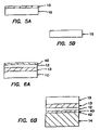
- FIGS. 5 a and 5 b are diagrams illustrating respectively the post-layer transfer device substrate comprised of the near surface ion implantation damage layer and the undamaged bulk, and the removal of the damage by etching from the bulk device substrate allowing the process to be repeated.
- FIGS. 6 a and 6 b are diagrams illustrating respectively the surface modification of the implanted device substrate with either a film of the same chemical identity as the handle substrate, and a wafer bonded substrate stack using this technique showing the device substrate.
- FIG. 7 is a graph of the strain state as a function of temperature for a Ge/Si wafer bonded virtual substrate.
- FIG. 8 is a graph of the strain state as a function of temperature for an InP/Si wafer bonded virtual substrate.
- FIG. 9 is a graph of the strain state as a function of temperature for a GaAs/Si wafer bonded virtual substrate.
- FIG. 10 is a graph of a wafer bonding temperature-pressure curve as a function of time as used in the bond annealing process.
- FIGS. 11 a and 11 b are diagrams illustrating respectively the wafer bonded virtual substrate following the anneal and layer exfoliation and the wafer bonded virtual substrate following a damage removal etch, polish or epitaxial growth on the device film.
- FIG. 12 is a graph of the rms surface roughness of a transferred InP device film as a function of time for 1:2:1, 1:2:2, 1:2:4, and 1:2:5 dilutions of the HCl:H 3 PO 4 :H 2 O 2 etch chemistry
- FIGS. 13 a and 13 b are diagrams illustrating respectively the completed wafer bonded virtual substrate and a wafer bonded virtual substrate with an epitaxially grown device fabricated on the device thin film.
- FIG. 14 is a diagram showing an optoelectronic structure grown on a wafer bonded virtual substrate consisting of the device film, the bonded interface, the handle substrate, and a strain compensation layer deposited on the back surface of the substrate.
- the fabrication 104 of virtual wafer bonded substrates could take two possible approaches as diagrammatically illustrated in the block diagram of FIG. 1 . These approaches are the integration of a thin device film with a bulk substrate prior to fabricating a functional device indicated by block 100 , or the device film can be transferred to the handle substrate following the fabrication of a functional logic device in the handle substrate and/or the fabrication of a functional optoelectronic device in the optoelectronic device substrate as depicted by block 102 .
- the term “device substrate” 10 is the optoelectronic substrate from which a thin film 12 will be removed.
- handle substrate 14 is defined in the specification to refer to the substrate that is used as a mechanical support for the device film 12 , namely the remainder of device substrate 10 after removal of film 12 .
- virtual substrate 16 is defined to be the completed structure of a thin device film 12 on a handle substrate 14 .
- III/V compound semiconductors i.e. GaAs, InP, GaN, etc.
- II/VI semiconductors i.e. CdTe, etc.
- group IV semiconductors i.e. Ge for GaAs family growth
- optically important Ferroelectric oxides i.e. LiNbO 4 , BaTiO 4 , etc.
- the handle substrate 14 will generally be Si, which is abundantly available and has desirable electrical, mechanical, and thermal properties. However, low-cost insulating substrates (i.e. glass, sapphire, etc.) might also be employed as handle substrate 14 .
- a generic process for fabricating such virtual substrates 16 comprises the following steps:
- FIG. 3 a which illustrates pre-bonding ion implantation of the device substrate 10 with an ion beam 11 , creating a modified structure as shown in FIG. 3 b comprising a device thin film 12 , an ion damaged layer for film transfer 13 , and the largely unaffected bulk of the device substrate 10 which is now called the handle substrate 14 .
- This process is generally performed with H + or a combination of H + and He + .
- other gas species may be employed to produce an intra-substrate etch process to assist in the exfoliation of the layer.
- a minimum implantation temperature to avoid amorphization and a needed implantation temperature, namely a minimum required dose relationship for this process.
- a necessary step in enabling this finished device structure will be the elimination of adsorbed water on the surface by means of a low temperature bake in an inert atmosphere or in vacuum. The bake should reach a temperature such that the vapor pressure of water at that temperature is well above the partial pressure of water in the surrounding ambient.
- FIGS. 6 a and 6 b illustrate the generic process.
- FIG. 6 a illustrates the surface modification of the implanted device substrate with either a crystalline or amorphous film 40 of the same chemical identity as the handle substrate 14 .
- FIG. 6 b illustrates a wafer bonded substrate stack using this technique showing the device substrate 10 , the ion implanted damage region 13 , the device thin film 12 , the deposited bond mediating film 40 , the bonded interface 42 , and the handle substrate 14 .
- FIG. 4 a is a diagram of a device substrate 10 and handle substrate 14 stack following ion implantation and initial bonding, showing the undamaged bulk device substrate 10 , the ion implanted damage layer 13 , the device thin film 12 , the wafer bonded device/handle interface 42 , and the handle substrate 14 .
- FIG. 4 a is a diagram of a device substrate 10 and handle substrate 14 stack following ion implantation and initial bonding, showing the undamaged bulk device substrate 10 , the ion implanted damage layer 13 , the device thin film 12 , the wafer bonded device/handle interface 42 , and the handle substrate 14 .
- FIG. 4 b is a diagram showing the wafer bonded virtual substrate 16 following the anneal and layer exfoliation, and showing the undamaged bulk device substrate 10 with its ion implanted damaged surface region 13 . Also shown is the wafer bonded virtual substrate 16 comprised of the ion implantation damaged surface region 13 of the device film 12 , the undamaged transferred device film 12 , the wafer bonded interface 42 , and the handle substrate 14 .
- the substrates 10 and/or 14 are held at an elevated temperature and a throttled gas/particle jet of CO 2 is impinged on the surface of substrates 10 , 14 removing particles by a combined physical impact and thermophoretic lifting effect.
- ⁇ ⁇ ( T ) ⁇ T 0 T ⁇ ⁇ ⁇ ⁇ ⁇ ( T ′ ) ⁇ d T ′
- ⁇ (T) is the difference in the thermal expansion coefficients ⁇ between the two substrates as a function of temperature, T, and where T 0 is the temperature of the zero strain condition, typically assumed to be the bond initiation temperature.
- T the temperature at which two substrates are brought into contact
- the strain state at temperatures of interest can be engineered. This could be advantageous for improving substrate performance in high-temperature processes, or a device operation temperature strain could be engineered to adjust a key device property such as bandgap or carrier mobility.
- the following descriptions describe the general types of strain temperature-strain dependences that could be achieved as a function of the sign of ⁇ (T).
- ⁇ ( T ) ⁇ handle ( T ) ⁇ device ( T )
- ⁇ ⁇ ( T ) ⁇ T 0 T ⁇ ⁇ ⁇ ⁇ ⁇ ( T ′ ) ⁇ d T ′ + ⁇ 0
- ⁇ 0 ⁇ T 0 T d ⁇ ⁇ d ⁇ ( T ′ ) ⁇ d T ′ + ⁇ T h T 0 ⁇ ⁇ h ⁇ ( T ′ ) ⁇ d T ′
- T d and T h are the temperatures of the device substrate 10 and the handle substrate 14 respectively at the instant of bond initiation.
- the temperature T 0 is the effective bond initiation temperature.
- the dissimilar temperatures of the substrates at bond initiation make this term difficult to determine.
- T 0 must have a value between T d and T h and will depend upon the experimental apparatus used in fabrication of the virtual substrate 16 and can be determined experimentally. The built-in strain approaches
- ⁇ 0 ⁇ T h T d ⁇ ⁇ ⁇ ( T ′ ) ⁇ d T ′
- thermo-mechanical strain can be accommodated in the bonded bulk substrate stack. Additionally, bonding is strengthened by means of improved substrate-substrate contact. A bonding process using multiple pressure-temperature steps or even a continuously varying pressure-temperature curve can be used to optimize the effectiveness of pressure in the process.
- the near surface region of the device film 12 is both rough and defect rich. This layer must be controllably removed to leave a surface that is useful for subsequent processing to fabricate an optoelectronic device as shown in FIGS. 11 a and 11 b . Depending on the device layer 10 this can be accomplished by:
- the finished virtual substrate 16 is meant to serve as a template for growth of an optoelectronic device through hetero-epitaxy. Through careful device layer modification, epitaxy of a wide range of optoelectronic devices is made possible. A representative image of such a structure is shown in FIGS. 13 a and 13 b .
- FIG. 13 a is a diagram which shows the completed wafer bonded virtual substrate 16 comprised of a thin device film 12 , a wafer bonded interface 42 and a handle substrate 14 .
- FIG. 13 b is a diagram which shows a wafer bonded virtual substrate 16 with an epitaxially grown device 50 fabricated on the device thin film 12 .
- FIG. 14 is a diagram which schematically shows an optoelectronic structure 50 grown on a wafer bonded virtual substrate 16 comprised of the device film 12 , the bonded interface 42 , the handle substrate 14 , and a strain compensation layer 18 deposited on the back surface of the substrate.
- the strain compensation layer 18 must have the same sign of ⁇ relative to the handle substrate as the device film 12 .
- the zero bow condition is not a zero strain condition, but rather a condition in which the strain energy of the device film 12 and the strain compensation layer 18 are exactly matched providing no driving force for substrate deformation.
- the material and deposition technique can be chosen to minimize the fabrication cost associated with this processing step.
- the strain energy associated with a thin film 12 is increased with substrate diameter, film strain, and film thickness.
- the strain compensation layer material 18 , deposition temperature, and thickness can be chosen to tailor the zero bow process temperature. The following are examples of how strain compensation could be performed for several materials systems:
Abstract
Description
-
- 1) The
device substrate 10 and handlesubstrate 14 may need pre-bonding treatment to allow for the removal of a thin film 12 (e.g. ion-implantation intodevice substrate 10 as diagrammatically depicted bynumber 11 inFIG. 3 a). - 2) The
device substrate 10 is cleaned and/or passivated to facilitate bonding. - 3) Bonding is initiated as diagrammatically shown in
FIG. 4 a. - 4) The
bond 42 is strengthened. - 5) The
device substrate 10 is thinned to leave a single-crystal film 12 on the finishedvirtual substrate 16 as shown inFIG. 4 b for an ion-implanted substrate. - 6) In the case of ion implantation induced layer exfoliation, the
device substrate 10 from which thedevice film 12 was derived can be reprocessed by a means of surface polishing to allow the reuse of thesubstrate 10 to transfer another device film as illustrated inFIG. 5 a andFIG. 5 b.
- 1) The
-
- a. H+ Implantation—A sufficient dose of H+ is implanted to allow film exfoliation upon annealing. This dose is a function of:
- Implant energy
- Implant temperature
- Device substrate material
- Film exfoliation anneal temperature
- b. H+/He+ Co-implantation—A sufficient total dose of H+ and He+ is implanted to allow film exfoliation upon annealing. The concept of this approach being that the H plays a chemical role of passivating internal surfaces, while the chemically inert He efficiently migrates to internal surfaces to provide pressure, and creates more damage per implanted ion than H increasing the internal surface density. The necessary dose is a function of:
- Implant energy
- Implant temperature
- H/He ratio
- Device substrate material
- Film exfoliation anneal temperature
- c. Etchant implantation—In addition to or replacement of H+ implantation, chemical species known to etch a given material can be implanted to create internally trapped chemical species that are volatile and cause exfoliation upon annealing. The chemical species chosen will be material specific according to known etchant properties or empirical experience.
- a. H+ Implantation—A sufficient dose of H+ is implanted to allow film exfoliation upon annealing. This dose is a function of:
-
- a. Group IV Passivation—The Group IV elemental semiconductors, particularly Ge, are rendered hydrophobic by the use of a dilute HF etching process. This leaves a predominantly hydride terminated surface.
- b. Group III/V Passivation—The Group III/V compound semiconductors can be rendered hydrophobic by compound-specific chemical treatments to leave a hydrophobically passivated surface for bonding.
- c. Group II/VI Passivation—The Group II/VI compound semiconductors can be rendered hydrophobic by compound-specific chemical treatments to leave a hydrophobically passivated surface for bonding.
- d. Ferroelectric Oxides—Applications involving ferroelectric oxides are fundamentally different than those for the optoelectronic materials from the elemental and compound semiconductors. For this reason handle substrate materials will be chosen for their electrical and refractive properties, but there will generally be no need to attempt hydrophobic wafer bonding to the insulating ferroelectric thin films. Thus, surface passivation will generally focus on forming a thin oxide on both the device and handle
substrates
-
- a. Deposition of a
layer 40 of material X on thedevice substrate 10 to enable an X-handle material bond. - b. Deposition of a
layer 40 of material X on thehandle substrate 14 to enable an X-device material bond. - c. Deposition of a
layer 40 of material X on both substrates to enable an X—X bond.
- a. Deposition of a
-
- d. Epitaxial Si bonding layer—This technique involves epitaxially growing a strained thin film of Si on the device substrate material. In this embodiment material X is strained thin film Si. Through doing this an intimate and maximally strong bond can be ensured between the device material and the Si epitaxial layer. The
device substrate 10 with the strained Si epitaxy is then implanted through the epitaxial layer (not shown) in preparation for wafer bonding and layer exfoliation. For material systems utilizing Si handlesubstrates 14 this would allow direct Si—Si wafer bonding using well established passivation techniques. - e. Amorphous Si bonding layer—This technique involves depositing a thin layer of amorphous Si (not shown) at low temperature on the
device substrate 10 to enable the use of typical Si surface preparation chemistries. In this embodiment material X is amorphous Si. This process could be performed either prior to or after ion implantation of thedevice substrate 10. For material systems utilizing Si handlesubstrates 14 this would allow direct Si—Si wafer bonding using well established passivation techniques.
- d. Epitaxial Si bonding layer—This technique involves epitaxially growing a strained thin film of Si on the device substrate material. In this embodiment material X is strained thin film Si. Through doing this an intimate and maximally strong bond can be ensured between the device material and the Si epitaxial layer. The
Δα(T)=αhandle(T)−αdevice(T)
-
- a. Δα(T)>0:
- 1. Room Temperature Bonding—In this case the
film 12 will be in tension at elevated processing temperatures. This will lead to changes in the lattice matching in heteroepitaxy on thevirtual substrate 16 and a tendency to concave substrate bowing. - 2. Elevated Temperature Bonding—In this case the film will have a zero strain condition at the bonding temperature such that tensile strain and concave wafer bowing will be reduced at higher processing temperatures. Likewise, the
film 12 will be in compressive strain at room temperature and likely at device operating temperatures leading to convex wafer bow. This could change device operation and enable design of novel devices based on strain control of materials parameters.
- 1. Room Temperature Bonding—In this case the
- b. Δα(T)<0:
- 1. Room Temperature Bonding—In this case the film will be in compression at elevated temperatures. This will lead to changes in the lattice matching in heteroepitaxy on the virtual substrate and a tendency to convex substrate bowing.
- 2. Elevated Temperature Bonding—In this case the
film 12 will have a zero strain condition at the bonding temperature such that compressive strain and convex bowing will be reduced at higher processing temperatures. Likewise, thefilm 12 will be in tensile strain at room temperature and likely at device operating temperatures leading to concave wafer bow. This could change device operation and enable design of novel devices based on strain control of materials parameters. Most materials of interest for the wafer bondedvirtual substrates 16 described belong to this category.- a. Ge/Si Bonding—
FIG. 7 is a graph which illustrates the predicted strain in Ge/Si bonding as a function of temperature for substrates bonded at various values of T0. The film compression at high temperatures can be reduced by initiation bonding at higher temperatures, T0. - b. InP/Si Bonding—
FIG. 8 is a graph which illustrates the predicted strain in InP/Si bonding as a function of temperature for substrates bonded at various values of T0. Again, the film compression at high temperatures can be reduced by initiation bonding at higher temperatures, T0. - c. GaAs/Si Bonding—
FIG. 9 is a graph which illustrates the predicted strain in GaAs/Si bonding as a function of temperature for substrates bonded at various values of T0. Once again, the film compression at high temperatures can be reduced by initiation bonding at higher temperatures, T0.
- a. Ge/Si Bonding—
- a. Δα(T)>0:
-
- a. Δα(T)>0:
- 1. Td>Th—These conditions enable the addition of a positive stress component causing the device film to be under increased tension at elevated temperatures.
- 2. Td<Th—These conditions enable the addition of a negative stress component reducing the high temperature tensile stress, but creating a greater low temperature compressive stress.
- b. Δα(T)<0:
- 1. Td>Th—These conditions enable the addition of a positive stress component causing the device film to be under a reduced degree of compressive stress at high temperatures.
- 2. Td<Th—These conditions enable the addition of a negative stress component increasing the high temperature compressive stress, but creating a reduced low temperature tensile stress.
- c. Δα(T)=0:
- 1. Td>Th—A temperature independent tensile stress can be imparted on the device film in this way.
- 2. Td<Th—A temperature independent compressive stress can be added to the device film.
- a. Δα(T)>0:
-
- a. Variable Pressure Cycle—One possible embodiment is to utilize independently varied pressure and temperature to optimize the bonding process. At low temperatures, high pressures are applied to strengthen the bond. At high temperatures the pressure is then reduced to avoid the suppression of layer exfoliation in the device substrate. A representative process is illustrated in the graph of
FIG. 10 where the wafer bonding temperature-pressure curve is shown as a function of time in the bond annealing process. - b. Single Pressure Cycle—The bonding process is also improved by applying a uni-axial load to the bonded pair for the duration of the anneal. In this process it is essential that the load be small enough to avoid the suppression of blistering.
- a. Variable Pressure Cycle—One possible embodiment is to utilize independently varied pressure and temperature to optimize the bonding process. At low temperatures, high pressures are applied to strengthen the bond. At high temperatures the pressure is then reduced to avoid the suppression of layer exfoliation in the device substrate. A representative process is illustrated in the graph of
-
- a. Wet Chemical Polishing—This process uses a device-film-dependent etch to controllably remove the ion implantation induced
damage layer 13 of the wafer bondedvirtual substrate 16, while simultaneously smoothing the surface of the transferred layer. Etches for specific materials are given below.- 1. Ge/Si:
- i. HF:H2O2:H2O—This etch can be performed at various dilution ratios x:y:z at various temperatures.
- ii. HF:HNO3:C2H4O2:H2O—This etch can be performed at various dilution ratios w:x:y:z at various temperatures.
- iii. H2O2:H2O—This etch can be performed at various dilution ratios y:z at various temperatures.
- 2. InP/Si:
- i. HCl:H3PO4:H2O2—This etching solution has been successfully used in ratios of 1:2:2 and 1:2:4. The H2O2 acts as an oxidizing agent and the mixture of HCl and H3PO4 etches the oxide. The combination of oxidation followed by etching creates a smoothened surface and removes the implantation damage.
FIG. 12 is a graph which shows both the surface roughness as a function of time for various etch dilutions.
- i. HCl:H3PO4:H2O2—This etching solution has been successfully used in ratios of 1:2:2 and 1:2:4. The H2O2 acts as an oxidizing agent and the mixture of HCl and H3PO4 etches the oxide. The combination of oxidation followed by etching creates a smoothened surface and removes the implantation damage.
- 1. Ge/Si:
- b. Chemical Mechanical Polishing—This utilizes both a chemical and a mechanical slurry to etch through implantation damage and leave a smooth surface.
- 1. Ge/Si—A colloidal silica slurry in a KOH chemistry can be used to polish the substrate.
- 2. InP/Si—A colloidal silica slurry in a sodium hypochlorite solution has been shown to smooth the surface of these virtual substrate materials.
- c. Homoepitaxial Smoothing—Even in circumstances when chemical etching removes the implantation damage, but doesn't leave an optimally smooth surface for subsequent heteroepitaxy, homoepitaxy of the device film material on the etched sample has been shown to reduce surface roughness. This can be performed as the first step in the growth of a heteroepitaxial structure on the wafer bonded virtual substrate.
- a. Wet Chemical Polishing—This process uses a device-film-dependent etch to controllably remove the ion implantation induced
-
- a. Ge/Si—The simplest case would be to deposit a film of Ge on the back surface of the Si handle substrate.
- b. InP/Si—Rather than deposit InP on the back of the handle, a thin film of Ge could be utilized because of its ease of deposition.
- c. GaAs/Si—As in the InP/Si case, Ge would make a good strain compensation layer.
- d. Other Materials—For all of the systems mentioned above, a low-cost material that is easily deposited is a suitable strain compensation layer, provided that the sign of Δα is appropriate.
Claims (22)
Priority Applications (7)
| Application Number | Priority Date | Filing Date | Title |
|---|---|---|---|
| US10/761,918 US7238622B2 (en) | 2001-04-17 | 2004-01-20 | Wafer bonded virtual substrate and method for forming the same |
| PCT/US2004/003347 WO2005079198A2 (en) | 2004-01-20 | 2004-02-05 | Wafer bonded virtual substrate and method for forming the same |
| US10/784,586 US20050026432A1 (en) | 2001-04-17 | 2004-02-23 | Wafer bonded epitaxial templates for silicon heterostructures |
| PCT/US2004/005266 WO2005060723A2 (en) | 2003-12-02 | 2004-02-23 | Wafer bonded epitaxial templates for silicon heterostructures |
| TW93137424A TW200529459A (en) | 2003-12-02 | 2004-12-02 | Wafer bonded epitaxial templates for silicon heterostructures |
| US11/004,948 US20050085049A1 (en) | 2001-04-17 | 2004-12-07 | Wafer bonded virtual substrate and method for forming the same |
| US11/004,808 US7341927B2 (en) | 2001-04-17 | 2004-12-07 | Wafer bonded epitaxial templates for silicon heterostructures |
Applications Claiming Priority (4)
| Application Number | Priority Date | Filing Date | Title |
|---|---|---|---|
| US28472601P | 2001-04-17 | 2001-04-17 | |
| US10/125,133 US7019339B2 (en) | 2001-04-17 | 2002-04-17 | Method of using a germanium layer transfer to Si for photovoltaic applications and heterostructure made thereby |
| US52633203P | 2003-12-02 | 2003-12-02 | |
| US10/761,918 US7238622B2 (en) | 2001-04-17 | 2004-01-20 | Wafer bonded virtual substrate and method for forming the same |
Related Parent Applications (1)
| Application Number | Title | Priority Date | Filing Date |
|---|---|---|---|
| US10/125,133 Continuation-In-Part US7019339B2 (en) | 2001-04-17 | 2002-04-17 | Method of using a germanium layer transfer to Si for photovoltaic applications and heterostructure made thereby |
Related Child Applications (3)
| Application Number | Title | Priority Date | Filing Date |
|---|---|---|---|
| US10/784,586 Continuation-In-Part US20050026432A1 (en) | 2001-04-17 | 2004-02-23 | Wafer bonded epitaxial templates for silicon heterostructures |
| US11/004,808 Continuation-In-Part US7341927B2 (en) | 2001-04-17 | 2004-12-07 | Wafer bonded epitaxial templates for silicon heterostructures |
| US11/004,948 Continuation-In-Part US20050085049A1 (en) | 2001-04-17 | 2004-12-07 | Wafer bonded virtual substrate and method for forming the same |
Publications (2)
| Publication Number | Publication Date |
|---|---|
| US20040214434A1 US20040214434A1 (en) | 2004-10-28 |
| US7238622B2 true US7238622B2 (en) | 2007-07-03 |
Family
ID=34886500
Family Applications (2)
| Application Number | Title | Priority Date | Filing Date |
|---|---|---|---|
| US10/761,918 Expired - Lifetime US7238622B2 (en) | 2001-04-17 | 2004-01-20 | Wafer bonded virtual substrate and method for forming the same |
| US11/004,948 Abandoned US20050085049A1 (en) | 2001-04-17 | 2004-12-07 | Wafer bonded virtual substrate and method for forming the same |
Family Applications After (1)
| Application Number | Title | Priority Date | Filing Date |
|---|---|---|---|
| US11/004,948 Abandoned US20050085049A1 (en) | 2001-04-17 | 2004-12-07 | Wafer bonded virtual substrate and method for forming the same |
Country Status (2)
| Country | Link |
|---|---|
| US (2) | US7238622B2 (en) |
| WO (1) | WO2005079198A2 (en) |
Cited By (13)
| Publication number | Priority date | Publication date | Assignee | Title |
|---|---|---|---|---|
| US20090194153A1 (en) * | 2008-02-05 | 2009-08-06 | Twin Creeks Technologies, Inc. | Photovoltaic cell comprising a thin lamina having low base resistivity and method of making |
| US20090194162A1 (en) * | 2008-02-05 | 2009-08-06 | Twin Creeks Technologies, Inc. | Method to form a photovoltaic cell comprising a thin lamina |
| US20090242031A1 (en) * | 2008-03-27 | 2009-10-01 | Twin Creeks Technologies, Inc. | Photovoltaic Assembly Including a Conductive Layer Between a Semiconductor Lamina and a Receiver Element |
| US20100032699A1 (en) * | 2008-08-05 | 2010-02-11 | Dicon Fiberoptics Inc. | System for High Efficiency Solid-State Light Emissions and Method of Manufacture |
| US20100093127A1 (en) * | 2006-12-27 | 2010-04-15 | Emcore Solar Power, Inc. | Inverted Metamorphic Multijunction Solar Cell Mounted on Metallized Flexible Film |
| US20100184248A1 (en) * | 2008-02-05 | 2010-07-22 | Twin Creeks Technologies, Inc. | Creation and Translation of Low-Relieff Texture for a Photovoltaic Cell |
| US20110041898A1 (en) * | 2009-08-19 | 2011-02-24 | Emcore Solar Power, Inc. | Back Metal Layers in Inverted Metamorphic Multijunction Solar Cells |
| US7939428B2 (en) | 2000-11-27 | 2011-05-10 | S.O.I.Tec Silicon On Insulator Technologies | Methods for making substrates and substrates formed therefrom |
| US20110124151A1 (en) * | 2007-04-06 | 2011-05-26 | Semiconductor Energy Laboratory Co., Ltd. | Photovoltaic device and method for manufacturing the same |
| US20110237013A1 (en) * | 2010-03-23 | 2011-09-29 | Twin Creeks Technologies, Inc. | Creation of Low-Relief Texture for a Photovoltaic Cell |
| WO2016041044A1 (en) * | 2014-09-19 | 2016-03-24 | Centro Nacional De Pesquisa Em Energia E Materiais | Process for production of silicon-integrated iii-v optoelectronic devices |
| US10354910B2 (en) | 2016-05-27 | 2019-07-16 | Raytheon Company | Foundry-agnostic post-processing method for a wafer |
| US10490688B2 (en) | 2011-10-11 | 2019-11-26 | Soitec | Multi junctions in a semiconductor device formed by different deposition techniques |
Families Citing this family (43)
| Publication number | Priority date | Publication date | Assignee | Title |
|---|---|---|---|---|
| US20050026432A1 (en) * | 2001-04-17 | 2005-02-03 | Atwater Harry A. | Wafer bonded epitaxial templates for silicon heterostructures |
| US7238622B2 (en) * | 2001-04-17 | 2007-07-03 | California Institute Of Technology | Wafer bonded virtual substrate and method for forming the same |
| EP1386349A1 (en) * | 2001-04-17 | 2004-02-04 | California Institute Of Technology | A method of using a germanium layer transfer to si for photovoltaic applications and heterostructure made thereby |
| US6885781B2 (en) * | 2002-05-03 | 2005-04-26 | Fujitsu Limited | Thin film electro-optical deflector device and a method of fabrication of such a device |
| US7157119B2 (en) * | 2002-06-25 | 2007-01-02 | Ppg Industries Ohio, Inc. | Method and compositions for applying multiple overlying organic pigmented decorations on ceramic substrates |
| US20060014363A1 (en) * | 2004-03-05 | 2006-01-19 | Nicolas Daval | Thermal treatment of a semiconductor layer |
| US7282449B2 (en) * | 2004-03-05 | 2007-10-16 | S.O.I.Tec Silicon On Insulator Technologies | Thermal treatment of a semiconductor layer |
| FR2867307B1 (en) * | 2004-03-05 | 2006-05-26 | Soitec Silicon On Insulator | HEAT TREATMENT AFTER SMART-CUT DETACHMENT |
| FR2867310B1 (en) * | 2004-03-05 | 2006-05-26 | Soitec Silicon On Insulator | TECHNIQUE FOR IMPROVING THE QUALITY OF A THIN LAYER TAKEN |
| US20080211061A1 (en) * | 2004-04-21 | 2008-09-04 | California Institute Of Technology | Method For the Fabrication of GaAs/Si and Related Wafer Bonded Virtual Substrates |
| US20060021565A1 (en) * | 2004-07-30 | 2006-02-02 | Aonex Technologies, Inc. | GaInP / GaAs / Si triple junction solar cell enabled by wafer bonding and layer transfer |
| US7732706B1 (en) * | 2004-09-17 | 2010-06-08 | The United States Of America As Represented By The Administrator Of The National Aeronautics And Space Administration | Solar cell circuit and method for manufacturing solar cells |
| US7846759B2 (en) * | 2004-10-21 | 2010-12-07 | Aonex Technologies, Inc. | Multi-junction solar cells and methods of making same using layer transfer and bonding techniques |
| US10374120B2 (en) * | 2005-02-18 | 2019-08-06 | Koninklijke Philips N.V. | High efficiency solar cells utilizing wafer bonding and layer transfer to integrate non-lattice matched materials |
| CN101248519B (en) | 2005-02-28 | 2011-08-24 | 硅源公司 | Substrate stiffness method and resulting devices for layer transfer processes |
| TW200707799A (en) * | 2005-04-21 | 2007-02-16 | Aonex Technologies Inc | Bonded intermediate substrate and method of making same |
| US7674687B2 (en) * | 2005-07-27 | 2010-03-09 | Silicon Genesis Corporation | Method and structure for fabricating multiple tiled regions onto a plate using a controlled cleaving process |
| US20070029043A1 (en) * | 2005-08-08 | 2007-02-08 | Silicon Genesis Corporation | Pre-made cleavable substrate method and structure of fabricating devices using one or more films provided by a layer transfer process |
| US7166520B1 (en) * | 2005-08-08 | 2007-01-23 | Silicon Genesis Corporation | Thin handle substrate method and structure for fabricating devices using one or more films provided by a layer transfer process |
| US7427554B2 (en) * | 2005-08-12 | 2008-09-23 | Silicon Genesis Corporation | Manufacturing strained silicon substrates using a backing material |
| US7456080B2 (en) * | 2005-12-19 | 2008-11-25 | Corning Incorporated | Semiconductor on glass insulator made using improved ion implantation process |
| US7863157B2 (en) * | 2006-03-17 | 2011-01-04 | Silicon Genesis Corporation | Method and structure for fabricating solar cells using a layer transfer process |
| US7598153B2 (en) * | 2006-03-31 | 2009-10-06 | Silicon Genesis Corporation | Method and structure for fabricating bonded substrate structures using thermal processing to remove oxygen species |
| EP2002484A4 (en) | 2006-04-05 | 2016-06-08 | Silicon Genesis Corp | Method and structure for fabricating solar cells using a layer transfer process |
| US20070243703A1 (en) * | 2006-04-14 | 2007-10-18 | Aonex Technololgies, Inc. | Processes and structures for epitaxial growth on laminate substrates |
| US7790565B2 (en) * | 2006-04-21 | 2010-09-07 | Corning Incorporated | Semiconductor on glass insulator made using improved thinning process |
| US20070262296A1 (en) * | 2006-05-11 | 2007-11-15 | Matthias Bauer | Photodetectors employing germanium layers |
| US20070277875A1 (en) * | 2006-05-31 | 2007-12-06 | Kishor Purushottam Gadkaree | Thin film photovoltaic structure |
| US8153513B2 (en) * | 2006-07-25 | 2012-04-10 | Silicon Genesis Corporation | Method and system for continuous large-area scanning implantation process |
| US7732301B1 (en) | 2007-04-20 | 2010-06-08 | Pinnington Thomas Henry | Bonded intermediate substrate and method of making same |
| US20090278233A1 (en) * | 2007-07-26 | 2009-11-12 | Pinnington Thomas Henry | Bonded intermediate substrate and method of making same |
| US20090206275A1 (en) * | 2007-10-03 | 2009-08-20 | Silcon Genesis Corporation | Accelerator particle beam apparatus and method for low contaminate processing |
| WO2010021623A1 (en) * | 2008-08-21 | 2010-02-25 | Midwest Research Institute | Epitaxial growth of silicon for layer transfer |
| US20110207306A1 (en) * | 2010-02-22 | 2011-08-25 | Sarko Cherekdjian | Semiconductor structure made using improved ion implantation process |
| US8196546B1 (en) | 2010-11-19 | 2012-06-12 | Corning Incorporated | Semiconductor structure made using improved multiple ion implantation process |
| US8008175B1 (en) | 2010-11-19 | 2011-08-30 | Coring Incorporated | Semiconductor structure made using improved simultaneous multiple ion implantation process |
| US8558195B2 (en) | 2010-11-19 | 2013-10-15 | Corning Incorporated | Semiconductor structure made using improved pseudo-simultaneous multiple ion implantation process |
| CN102437054B (en) * | 2011-11-16 | 2014-09-24 | 西安电子科技大学 | Manufacturing method of wafer-level uniaxial strain silicon germanium on insulater (SGOI) |
| US9238755B2 (en) * | 2011-11-25 | 2016-01-19 | Fujima Incorporated | Polishing composition |
| US9082692B2 (en) | 2013-01-02 | 2015-07-14 | Micron Technology, Inc. | Engineered substrate assemblies with epitaxial templates and related systems, methods, and devices |
| WO2016007582A1 (en) * | 2014-07-11 | 2016-01-14 | Gtat Corporation | Support substrate for ion beam exfoliation of a crystalline lamina |
| FR3043492B1 (en) * | 2015-11-09 | 2017-12-22 | Commissariat Energie Atomique | PROCESS FOR PRODUCING SUBSTRATES |
| US20180019169A1 (en) * | 2016-07-12 | 2018-01-18 | QMAT, Inc. | Backing substrate stabilizing donor substrate for implant or reclamation |
Citations (47)
| Publication number | Priority date | Publication date | Assignee | Title |
|---|---|---|---|---|
| EP0060103A1 (en) | 1981-03-05 | 1982-09-15 | Mobil Oil Corporation | Process for manufacturing ethylene |
| US4474647A (en) | 1981-04-24 | 1984-10-02 | Institut Francais Du Petrole | Process for purifying a C4 and/or C5 hydrocarbon cut containing water and dimethyl ether as impurities |
| US4499327A (en) | 1982-10-04 | 1985-02-12 | Union Carbide Corporation | Production of light olefins |
| US5013681A (en) | 1989-09-29 | 1991-05-07 | The United States Of America As Represented By The Secretary Of The Navy | Method of producing a thin silicon-on-insulator layer |
| JPH03270220A (en) | 1990-03-20 | 1991-12-02 | Fujitsu Ltd | Manufacture of seed crystal for growing bulk crystal |
| US5090977A (en) | 1990-11-13 | 1992-02-25 | Exxon Chemical Patents Inc. | Sequence for separating propylene from cracked gases |
| US5217564A (en) | 1980-04-10 | 1993-06-08 | Massachusetts Institute Of Technology | Method of producing sheets of crystalline material and devices made therefrom |
| US5231047A (en) | 1991-12-19 | 1993-07-27 | Energy Conversion Devices, Inc. | High quality photovoltaic semiconductor material and laser ablation method of fabrication same |
| US5315793A (en) | 1991-10-01 | 1994-05-31 | Hughes Aircraft Company | System for precision cleaning by jet spray |
| US5336841A (en) | 1993-04-05 | 1994-08-09 | Chemical Research & Licensing Company | Oxygenate removal in MTBE process |
| US5374564A (en) | 1991-09-18 | 1994-12-20 | Commissariat A L'energie Atomique | Process for the production of thin semiconductor material films |
| US5391257A (en) | 1993-12-10 | 1995-02-21 | Rockwell International Corporation | Method of transferring a thin film to an alternate substrate |
| US5395788A (en) | 1991-03-15 | 1995-03-07 | Shin Etsu Handotai Co., Ltd. | Method of producing semiconductor substrate |
| US5609734A (en) | 1993-11-05 | 1997-03-11 | Institut Francais Du Petrole | Combined distillation and permeation process for the separation of oxygenated compounds from hydrocarbons and use thereof in etherification |
| US5637187A (en) | 1990-09-05 | 1997-06-10 | Seiko Instruments Inc. | Light valve device making |
| US5641381A (en) | 1995-03-27 | 1997-06-24 | The United States Of America As Represented By The Administrator Of The National Aeronautics And Space Administration | Preferentially etched epitaxial liftoff of InP material |
| US5710057A (en) | 1996-07-12 | 1998-01-20 | Kenney; Donald M. | SOI fabrication method |
| US5720929A (en) | 1992-11-06 | 1998-02-24 | Institut Francais Du Petrole | Device for catalytic dehydrogenation of a C2+ paraffinic charge comprising means for inhibiting the freezing of water in the effluent |
| US5877070A (en) | 1997-05-31 | 1999-03-02 | Max-Planck Society | Method for the transfer of thin layers of monocrystalline material to a desirable substrate |
| US5882987A (en) | 1997-08-26 | 1999-03-16 | International Business Machines Corporation | Smart-cut process for the production of thin semiconductor material films |
| US5910699A (en) | 1995-05-08 | 1999-06-08 | Matsushita Electric Industrial Co., Ltd. | Method of manufacturing a composite substrate and a piezoelectric device using the substrate |
| US5914433A (en) | 1997-07-22 | 1999-06-22 | Uop Lll | Process for producing polymer grade olefins |
| US6020252A (en) | 1996-05-15 | 2000-02-01 | Commissariat A L'energie Atomique | Method of producing a thin layer of semiconductor material |
| US6103597A (en) | 1996-04-11 | 2000-08-15 | Commissariat A L'energie Atomique | Method of obtaining a thin film of semiconductor material |
| US6121504A (en) | 1998-04-29 | 2000-09-19 | Exxon Chemical Patents Inc. | Process for converting oxygenates to olefins with direct product quenching for heat recovery |
| US6150239A (en) | 1997-05-31 | 2000-11-21 | Max Planck Society | Method for the transfer of thin layers monocrystalline material onto a desirable substrate |
| WO2001003172A1 (en) | 1999-06-30 | 2001-01-11 | Commissariat A L'energie Atomique | Method for producing a thin membrane and resulting structure with membrane |
| US6211738B1 (en) | 1998-01-30 | 2001-04-03 | Conexant Systems, Inc. | Stability and enhanced gain of amplifiers using inductive coupling |
| US6221738B1 (en) | 1997-03-26 | 2001-04-24 | Canon Kabushiki Kaisha | Substrate and production method thereof |
| US6242324B1 (en) | 1999-08-10 | 2001-06-05 | The United States Of America As Represented By The Secretary Of The Navy | Method for fabricating singe crystal materials over CMOS devices |
| US6251754B1 (en) * | 1997-05-09 | 2001-06-26 | Denso Corporation | Semiconductor substrate manufacturing method |
| US6323108B1 (en) * | 1999-07-27 | 2001-11-27 | The United States Of America As Represented By The Secretary Of The Navy | Fabrication ultra-thin bonded semiconductor layers |
| US6328796B1 (en) | 1999-02-01 | 2001-12-11 | The United States Of America As Represented By The Secretary Of The Navy | Single-crystal material on non-single-crystalline substrate |
| US6346458B1 (en) | 1998-12-31 | 2002-02-12 | Robert W. Bower | Transposed split of ion cut materials |
| US6429104B1 (en) | 1998-02-02 | 2002-08-06 | S.O.I. Tec Silicon On Insulator Technologies | Method for forming cavities in a semiconductor substrate by implanting atoms |
| US6489241B1 (en) | 1999-09-17 | 2002-12-03 | Applied Materials, Inc. | Apparatus and method for surface finishing a silicon film |
| US6497763B2 (en) | 2001-01-19 | 2002-12-24 | The United States Of America As Represented By The Secretary Of The Navy | Electronic device with composite substrate |
| US6504091B2 (en) | 2000-02-14 | 2003-01-07 | Sharp Kabushiki Kaisha | Photoelectric converting device |
| US20030064535A1 (en) | 2001-09-28 | 2003-04-03 | Kub Francis J. | Method of manufacturing a semiconductor device having a thin GaN material directly bonded to an optimized substrate |
| US6794276B2 (en) | 2000-11-27 | 2004-09-21 | S.O.I.Tec Silicon On Insulator Technologies S.A. | Methods for fabricating a substrate |
| US6815309B2 (en) | 2001-12-21 | 2004-11-09 | S.O.I.Tec Silicon On Insulator Technologies S.A. | Support-integrated donor wafers for repeated thin donor layer separation |
| US20040235268A1 (en) | 2000-11-27 | 2004-11-25 | Fabrice Letertre | Fabrication of substrates with a useful layer of monocrystalline semiconductor material |
| US20050026432A1 (en) | 2001-04-17 | 2005-02-03 | Atwater Harry A. | Wafer bonded epitaxial templates for silicon heterostructures |
| US20050032330A1 (en) | 2002-01-23 | 2005-02-10 | Bruno Ghyselen | Methods for transferring a useful layer of silicon carbide to a receiving substrate |
| US6867067B2 (en) | 2000-11-27 | 2005-03-15 | S.O.I. Tec Silicon On Insulator Technologies S.A. | Methods for fabricating final substrates |
| US20050085049A1 (en) * | 2001-04-17 | 2005-04-21 | California Institute Of Technology | Wafer bonded virtual substrate and method for forming the same |
| US7019339B2 (en) * | 2001-04-17 | 2006-03-28 | California Institute Of Technology | Method of using a germanium layer transfer to Si for photovoltaic applications and heterostructure made thereby |
Family Cites Families (6)
| Publication number | Priority date | Publication date | Assignee | Title |
|---|---|---|---|---|
| US4679942A (en) * | 1984-02-24 | 1987-07-14 | Nippon Kogaku K. K. | Method of aligning a semiconductor substrate and a photomask |
| US5849627A (en) * | 1990-02-07 | 1998-12-15 | Harris Corporation | Bonded wafer processing with oxidative bonding |
| JPH08501900A (en) * | 1992-06-17 | 1996-02-27 | ハリス・コーポレーション | Bonded wafer manufacturing method |
| TW289837B (en) * | 1994-01-18 | 1996-11-01 | Hwelett Packard Co | |
| US6455398B1 (en) * | 1999-07-16 | 2002-09-24 | Massachusetts Institute Of Technology | Silicon on III-V semiconductor bonding for monolithic optoelectronic integration |
| US6562127B1 (en) * | 2002-01-16 | 2003-05-13 | The United States Of America As Represented By The Secretary Of The Navy | Method of making mosaic array of thin semiconductor material of large substrates |
-
2004
- 2004-01-20 US US10/761,918 patent/US7238622B2/en not_active Expired - Lifetime
- 2004-02-05 WO PCT/US2004/003347 patent/WO2005079198A2/en active Application Filing
- 2004-12-07 US US11/004,948 patent/US20050085049A1/en not_active Abandoned
Patent Citations (50)
| Publication number | Priority date | Publication date | Assignee | Title |
|---|---|---|---|---|
| US5217564A (en) | 1980-04-10 | 1993-06-08 | Massachusetts Institute Of Technology | Method of producing sheets of crystalline material and devices made therefrom |
| EP0060103A1 (en) | 1981-03-05 | 1982-09-15 | Mobil Oil Corporation | Process for manufacturing ethylene |
| US4474647A (en) | 1981-04-24 | 1984-10-02 | Institut Francais Du Petrole | Process for purifying a C4 and/or C5 hydrocarbon cut containing water and dimethyl ether as impurities |
| US4499327A (en) | 1982-10-04 | 1985-02-12 | Union Carbide Corporation | Production of light olefins |
| US5013681A (en) | 1989-09-29 | 1991-05-07 | The United States Of America As Represented By The Secretary Of The Navy | Method of producing a thin silicon-on-insulator layer |
| JPH03270220A (en) | 1990-03-20 | 1991-12-02 | Fujitsu Ltd | Manufacture of seed crystal for growing bulk crystal |
| US5637187A (en) | 1990-09-05 | 1997-06-10 | Seiko Instruments Inc. | Light valve device making |
| US5090977A (en) | 1990-11-13 | 1992-02-25 | Exxon Chemical Patents Inc. | Sequence for separating propylene from cracked gases |
| US5395788A (en) | 1991-03-15 | 1995-03-07 | Shin Etsu Handotai Co., Ltd. | Method of producing semiconductor substrate |
| US5374564A (en) | 1991-09-18 | 1994-12-20 | Commissariat A L'energie Atomique | Process for the production of thin semiconductor material films |
| US5315793A (en) | 1991-10-01 | 1994-05-31 | Hughes Aircraft Company | System for precision cleaning by jet spray |
| US5231047A (en) | 1991-12-19 | 1993-07-27 | Energy Conversion Devices, Inc. | High quality photovoltaic semiconductor material and laser ablation method of fabrication same |
| US5720929A (en) | 1992-11-06 | 1998-02-24 | Institut Francais Du Petrole | Device for catalytic dehydrogenation of a C2+ paraffinic charge comprising means for inhibiting the freezing of water in the effluent |
| US5336841A (en) | 1993-04-05 | 1994-08-09 | Chemical Research & Licensing Company | Oxygenate removal in MTBE process |
| US5609734A (en) | 1993-11-05 | 1997-03-11 | Institut Francais Du Petrole | Combined distillation and permeation process for the separation of oxygenated compounds from hydrocarbons and use thereof in etherification |
| US5391257A (en) | 1993-12-10 | 1995-02-21 | Rockwell International Corporation | Method of transferring a thin film to an alternate substrate |
| US5641381A (en) | 1995-03-27 | 1997-06-24 | The United States Of America As Represented By The Administrator Of The National Aeronautics And Space Administration | Preferentially etched epitaxial liftoff of InP material |
| US5910699A (en) | 1995-05-08 | 1999-06-08 | Matsushita Electric Industrial Co., Ltd. | Method of manufacturing a composite substrate and a piezoelectric device using the substrate |
| US6103597A (en) | 1996-04-11 | 2000-08-15 | Commissariat A L'energie Atomique | Method of obtaining a thin film of semiconductor material |
| US6020252A (en) | 1996-05-15 | 2000-02-01 | Commissariat A L'energie Atomique | Method of producing a thin layer of semiconductor material |
| US5710057A (en) | 1996-07-12 | 1998-01-20 | Kenney; Donald M. | SOI fabrication method |
| US6221738B1 (en) | 1997-03-26 | 2001-04-24 | Canon Kabushiki Kaisha | Substrate and production method thereof |
| US6251754B1 (en) * | 1997-05-09 | 2001-06-26 | Denso Corporation | Semiconductor substrate manufacturing method |
| US6150239A (en) | 1997-05-31 | 2000-11-21 | Max Planck Society | Method for the transfer of thin layers monocrystalline material onto a desirable substrate |
| US5877070A (en) | 1997-05-31 | 1999-03-02 | Max-Planck Society | Method for the transfer of thin layers of monocrystalline material to a desirable substrate |
| US5914433A (en) | 1997-07-22 | 1999-06-22 | Uop Lll | Process for producing polymer grade olefins |
| US5882987A (en) | 1997-08-26 | 1999-03-16 | International Business Machines Corporation | Smart-cut process for the production of thin semiconductor material films |
| US6211738B1 (en) | 1998-01-30 | 2001-04-03 | Conexant Systems, Inc. | Stability and enhanced gain of amplifiers using inductive coupling |
| US6429104B1 (en) | 1998-02-02 | 2002-08-06 | S.O.I. Tec Silicon On Insulator Technologies | Method for forming cavities in a semiconductor substrate by implanting atoms |
| US6121504A (en) | 1998-04-29 | 2000-09-19 | Exxon Chemical Patents Inc. | Process for converting oxygenates to olefins with direct product quenching for heat recovery |
| US6346458B1 (en) | 1998-12-31 | 2002-02-12 | Robert W. Bower | Transposed split of ion cut materials |
| US6328796B1 (en) | 1999-02-01 | 2001-12-11 | The United States Of America As Represented By The Secretary Of The Navy | Single-crystal material on non-single-crystalline substrate |
| WO2001003172A1 (en) | 1999-06-30 | 2001-01-11 | Commissariat A L'energie Atomique | Method for producing a thin membrane and resulting structure with membrane |
| US6465327B1 (en) | 1999-06-30 | 2002-10-15 | Commissariat A L'energie Atomique | Method for producing a thin membrane and resulting structure with membrane |
| US6323108B1 (en) * | 1999-07-27 | 2001-11-27 | The United States Of America As Represented By The Secretary Of The Navy | Fabrication ultra-thin bonded semiconductor layers |
| US6242324B1 (en) | 1999-08-10 | 2001-06-05 | The United States Of America As Represented By The Secretary Of The Navy | Method for fabricating singe crystal materials over CMOS devices |
| US6489241B1 (en) | 1999-09-17 | 2002-12-03 | Applied Materials, Inc. | Apparatus and method for surface finishing a silicon film |
| US6504091B2 (en) | 2000-02-14 | 2003-01-07 | Sharp Kabushiki Kaisha | Photoelectric converting device |
| US20040235268A1 (en) | 2000-11-27 | 2004-11-25 | Fabrice Letertre | Fabrication of substrates with a useful layer of monocrystalline semiconductor material |
| US6867067B2 (en) | 2000-11-27 | 2005-03-15 | S.O.I. Tec Silicon On Insulator Technologies S.A. | Methods for fabricating final substrates |
| US6794276B2 (en) | 2000-11-27 | 2004-09-21 | S.O.I.Tec Silicon On Insulator Technologies S.A. | Methods for fabricating a substrate |
| US6497763B2 (en) | 2001-01-19 | 2002-12-24 | The United States Of America As Represented By The Secretary Of The Navy | Electronic device with composite substrate |
| US20050026432A1 (en) | 2001-04-17 | 2005-02-03 | Atwater Harry A. | Wafer bonded epitaxial templates for silicon heterostructures |
| US20050085049A1 (en) * | 2001-04-17 | 2005-04-21 | California Institute Of Technology | Wafer bonded virtual substrate and method for forming the same |
| US20050142879A1 (en) * | 2001-04-17 | 2005-06-30 | California Institute Of Technology | Wafer bonded epitaxial templates for silicon heterostructures |
| US7019339B2 (en) * | 2001-04-17 | 2006-03-28 | California Institute Of Technology | Method of using a germanium layer transfer to Si for photovoltaic applications and heterostructure made thereby |
| US20030064535A1 (en) | 2001-09-28 | 2003-04-03 | Kub Francis J. | Method of manufacturing a semiconductor device having a thin GaN material directly bonded to an optimized substrate |
| US6815309B2 (en) | 2001-12-21 | 2004-11-09 | S.O.I.Tec Silicon On Insulator Technologies S.A. | Support-integrated donor wafers for repeated thin donor layer separation |
| US6908828B2 (en) | 2001-12-21 | 2005-06-21 | S.O.I. Tec Silicon On Insulator Technologies S.A. | Support-integrated donor wafers for repeated thin donor layer separation |
| US20050032330A1 (en) | 2002-01-23 | 2005-02-10 | Bruno Ghyselen | Methods for transferring a useful layer of silicon carbide to a receiving substrate |
Non-Patent Citations (53)
| Title |
|---|
| Akatsu et al., Wafer Bonding of Different III-V Compounds Semiconductors by Atomic Hydrogen Surface Cleaning, Journal of Applied Physics, Oct. 2001, pp. 3856-3862, vol. 90, No. 8, American Institute of Physics. |
| Auberton-Hervé et al., Smart-Cut(R): The Basic Fabrication Process for Unibond(R) SOI Wafers, IEICE Trans. Electron, Mar. 1997, pp. 358-363, vol. E80-C, No. 3, The Institute of Electronics, Information and Communication Engineers. |
| Bett et al., III-V Compounds for Solar Cell Applications, Appl. Phys. A, 1999, pp. 119-129, vol. 69, Springer-Verlag (published online: Jun. 24, 1999). |
| Bruel et al., Smart-Cut: A New Silicon On Insulator Material Technology Based on Hydrogen Implantation and Wafer Bonding, Mar. 1997, pp. 1636-1641, vol. 36, Jpn. J. Appl. Phys. |
| Bruel M., Application of Hydrogen Ion Beams to Silicon on Insulator Material Technology, Nuclear Instruments and Methods in Physics Research B, 1996, pp. 313-319, vol. 108, Elsevier Science B.V. |
| Bruel M., Silicon on Insulator Material Technology, Electronics Letters, Jul. 1995, pp. 1201-1202, vol. 31, No. 14. |
| Cheng et al., Electron Mobility Enhancement in Strained-Si n-MOSFETs Fabricated on SiGe-on-Insulator (SGOI) Substrates, IEEE Electron Device Letters, Jul. 2001, pp. 321-323, vol. 22, No. 7. |
| Curtis et al., "Integration of the UOP/HYDRO MTO Process into Ethylene Plants," 10<SUP>th </SUP>Ethylene Producers' Conference, 1998, pp. 54-85. |
| Dobaczewski et al., Donor Level of Bond-Center Hydrogen in Germanium, Physical Review B, 2004, pp. 245207-1-6, vol. 69. |
| Georgakilas et al., Wafer-scale Integration of GaAs Optoelectronic Devices with Standard Si Integrated Circuits Using a Low-Temperature Bonding Procedure, Applied Physics Letters, Dec. 2002, pp. 5099-5101, vol. 81, No. 27, American Institute of Physics [Downloaded Oct. 19, 2004]. |
| Gösele et al., Fundamental Issues in Wafer Bonding, J. Vac. Sci. Technol. A, Jul./Aug. 1999, pp. 1145-1152, vol. 17(4), American Vacuum Society. |
| Gösele et al., Semiconductor Wafer Bonding. Annu. Rev. Mater. Sci., 1998, pp. 215-241, vol. 28. |
| Huang et al., Electron and Hole Mobility Enhancement in Strained SOI by Wafer Bonding, IEEE Transactions on Electron Devices, Sep. 2002, pp. 1566-1571, vol. 49, No. 9. |
| Huang et al., SiGe-on-Insulator Prepared by Wafer Bonding and Layer Transfer for High-Performance Field-Effect Transistors, Applied Physics Letters, Feb. 2001, pp. 1267-1269, vol. 78, No. 9, American Institute of Physics. |
| Kim et al., Heterogeneous Silicon Integration by Ultra-High Vacuum Wafer Bonding, Journal of Electronic Materials, 2003, pp. 849-854, vol. 32, No. 8. |
| Lagnado et al., Integration of Si and SiGe with Al<SUB>2</SUB>O<SUB>3 </SUB>(sapphire), Microelectronic Engineering, 2001, pp. 455-459, vol. 59, Elsevier Science B.V. |
| Langdo et al., Strained Si on Insulator Technology: From Materials to Devices, Solid-State Electronics, 2004, pp. 1357-1367, vol. 48, Elsevier Ltd. |
| Leroy et al., Controlled Surface Nanopatterning with Buried Dislocation Arrays, Surface Science, 2003, pp. 211-219, vol. 545, Elsevier B.V. |
| Ma et al., Solid-State Reaction-Mediated Low-Temperature Bonding of GaAs and InP Wafers to Si Substrates, Appl. Phys. Lett., Feb. 1994, pp. 772-774, vol. 64, No. 6, American Institute of Physics. |
| Maleville et al., Smart-Cut(R) Technology: From 300 mm Ultrathin SOI Production to Advanced Engineered Substrates, Solid-State Electronics, 2004, pp. 1055-1063, vol. 48, Elsevier Ltd. |
| Morral et al., Assessment of Optical and Structural Properties of III-V Semiconductors Grown on InP/Si and Ge/Si Wafer Bonded Epitaxial Templates with Application to a Four-Junction Solar Cell, (Abstract), MRS 2003 Spring Meeting, (Apr. 2003). |
| Morral et al., Bonding and Layer Transfer Process of InP on Silicon for the Elaboration of the Botton Double Heterostructure of 4-Junction High Efficiency Solar Cells, (Abstract), MRS 2002 Fall Meeting, (Nov. 2002). |
| Morral et al., Electrical and Structural Characterization of the Interface of Wafer Bonded InP/Si, MRS 2003 Spring Meeting, (Apr. 2003). |
| Morral et al., InGaAs/InP Double Heterostructures on InP/Si Templates Fabricated by Wafer Bonding and Hydrogen-Induced Exfoliation, Applied Physics Letters, Dec. 2003, pp. 5413-5415, vol. 83, No. 26, American Institute of Physics. |
| Morral et al., The Role of Hydrogen in H-Induced Exfoliation and Layer Transfer on InP, (Abstract), MRS 2004 Spring Meeting, (Apr. 2004). |
| Taraschi et al., Strained Si, SiGe, and Ge On-Insulator: Review of Wafer Bonding Fabrication Techniques, Solid-State Electronics, 2004, pp. 1297-1305, vol. 48, Elsevier Ltd. |
| Tong et al., "Layer Splitting Process in Hydrogen-Implanted Si, Ge, SiC, and Diamond Substrates," Appl. Phys. Lett., vol. 70, No. 11, Mar. 17, 1997, pp. 1390-1392. |
| Tong et al., A "Smarter-Cut" Approach to Low Temperature Silicon Layer Transfer, Appl. Phys. Lett., Jan. 1998, pp. 49-51, vol. 72, No. 1, American Institute of Physics. |
| Tong et al., Hydrophobic Silicon Wafer Bonding, Appl. Phys. Lett., Jan. 1994, pp. 625-627, vol. 64, No. 5, American Institute of Physics. |
| Tong et al., Layer Splitting Process in Hydrogen-Implanted Si, Ge, SiC, and Diamond Substrates, Appl. Phys. Letter, Mar. 1997, pp. 1390-1392, vol. 70, No. 11, American Institute of Physics. |
| Tong et al., Wafer Bonding and Layer Splitting for Microsystems, Adv. Mater., 1999, pp. 1409-1425, vol. 11, No. 17, Wiley-VCH Verlag GmbH. |
| Tracy et al., Germanium-on-Insulator Substrates by Wafer Bonding, Journal of Electronic Materials, 2004, pp. 886-892, vol. 33, No. 8. |
| U.S. Appl. No. 10/784,586, filed Feb. 23, 2004, Atwater et al. |
| U.S. Appl. No. 11/004,808, filed Dec. 7, 2004, Atwater et al. |
| U.S. Appl. No. 11/004,948, filed Dec. 7, 2004, Atwater et al. |
| U.S. Appl. No. 11/430,160, filed May 9, 2006, Atwater, Jr. et al. |
| Weldon et al., "Mechanism of Silicon Exfoliation Induced by Hydrogen/Helium Co-Implantation," Applied Physics Letters, vol. 73, No. 25, Dec. 21, 1998, pp. 3721-3723. |
| Wiegand et al., Wafer Bonding of Silicon Wafers Covered with Various Surface Layers, Sensors and Actuators, 2000, pp. 91-95, vol. 86, Elsevier Science B.V. |
| Yamaguchi M., Multi-Junction Solar Cells and Novel Structures for Solar Cell Applications, Physica E, 2002, pp. 84-90, vol. 14, Elsevier Science B.V. |
| Zahler et al., GE Layer Transfer to Si for Photovoltaic Applications, (Presentation), 14 pages, MRS 2001 Spring Conference, (Apr. 2001). |
| Zahler et al., Ge Layer Transfer to Si for Photovoltaic Applications, Thin Solid Films, 2002, pp. 558-562, vol. 403-404, Elsevier Science B.V. |
| Zahler et al., Ge/Si Wafer Bonded Epitaxial Templates for GaAs/Si Heterostructures, (Abstract), MRS 2002 Fall Meeting, (Nov. 2002). |
| Zahler et al., J. Electron Mater., 33(8), (2004), pp. 22-23, (Abstracts K2 and K3). |
| Zahler et al., The Role of H in the H-Induced Exfoliation of GE Films, (Abstract and Presentation), MRS 2004 Spring Meeting, 16 pages (Apr. 2004). |
| Zahler et al., Wafer Bonded Expitaxial Templates for GaAs/Si and InP/Si Heterostructures, (Presentation), MRS 2003 Fall Meeting, 15 pages, (Nov. 2003). |
| Zahler et al., Wafer Bonded Expitaxial Templates for GaAs/Si Heterostructures, (Abstract and Presentation), MRS 2003 Spring Meeting, 16 pages, (Apr. 2003). |
| Zahler et al., Wafer Bonded Ge/Si Heterostructures for Photovoltaic Applications, (Abstract and Presentation), MRS 2002 Spring Meeting (Apr. 2002). |
| Zahler et al., Wafer Bonded Ge/Si Heterostructures for Photovoltaic Applications, (Presentation), Electronic Materials Conference 2002, 16 pages. |
| Zahler et al., Wafer Bonded Ge/Si Heterostructures for Photovoltaic Applications, Presentation, MRS 2002 Fall Meeting, 16 pages, (Nov. 2002). |
| Zahler et al., Wafer Bonding and Layer Transfer Processes for 4-Junction High Efficiency Solar Cells, 29<SUP>th </SUP>IEEE Photovoltaic Specialists Conference, New Orleans, USA, (May 2002). |
| Zahler et al., Wafer Bonding and Layer Transfer Processes for A 4-Junction Solar Cell, (Presentation) 29<SUP>th </SUP>IEEE Photovoltaic Specialists Conference, New Orleans, USA, (May 2002). |
| Zahler et al., Wafer Bonding Processes for Ultrahigh Efficiency Photovoltaic Applications, (Abstract and Presentation), MRS 2001 Fall Meeting, (Nov. 2001). |
| Zahler J.M., Materials Integration by Wafer Bonding and Layer Transfer, (Presentation), 13 pages, MRS 2004 Spring Meeting (Apr. 2004). |
Cited By (26)
| Publication number | Priority date | Publication date | Assignee | Title |
|---|---|---|---|---|
| US7939428B2 (en) | 2000-11-27 | 2011-05-10 | S.O.I.Tec Silicon On Insulator Technologies | Methods for making substrates and substrates formed therefrom |
| US20100093127A1 (en) * | 2006-12-27 | 2010-04-15 | Emcore Solar Power, Inc. | Inverted Metamorphic Multijunction Solar Cell Mounted on Metallized Flexible Film |
| US8828789B2 (en) | 2007-04-06 | 2014-09-09 | Semiconductor Energy Laboratory Co., Ltd. | Photovoltaic device and method for manufacturing the same |
| US20110124151A1 (en) * | 2007-04-06 | 2011-05-26 | Semiconductor Energy Laboratory Co., Ltd. | Photovoltaic device and method for manufacturing the same |
| US20090197368A1 (en) * | 2008-02-05 | 2009-08-06 | Twin Creeks Technologies, Inc. | Method to form a photovoltaic cell comprising a thin lamina |
| US20100009488A1 (en) * | 2008-02-05 | 2010-01-14 | Twin Creeks Technologies, Inc. | Method to form a photovoltaic cell comprising a thin lamina |
| US8247260B2 (en) | 2008-02-05 | 2012-08-21 | Twin Creeks Technologies, Inc. | Method to form a photovoltaic cell comprising a thin lamina |
| US20090197367A1 (en) * | 2008-02-05 | 2009-08-06 | Twin Creeks Technologies, Inc. | Method to form a photovoltaic cell comprising a thin lamina |
| US20100184248A1 (en) * | 2008-02-05 | 2010-07-22 | Twin Creeks Technologies, Inc. | Creation and Translation of Low-Relieff Texture for a Photovoltaic Cell |
| US7842585B2 (en) | 2008-02-05 | 2010-11-30 | Twin Creeks Technologies, Inc. | Method to form a photovoltaic cell comprising a thin lamina |
| US8563352B2 (en) | 2008-02-05 | 2013-10-22 | Gtat Corporation | Creation and translation of low-relief texture for a photovoltaic cell |
| US20090194153A1 (en) * | 2008-02-05 | 2009-08-06 | Twin Creeks Technologies, Inc. | Photovoltaic cell comprising a thin lamina having low base resistivity and method of making |
| US20090194164A1 (en) * | 2008-02-05 | 2009-08-06 | Twin Creeks Technologies, Inc. | Method to form a photovoltaic cell comprising a thin lamina |
| US20090194162A1 (en) * | 2008-02-05 | 2009-08-06 | Twin Creeks Technologies, Inc. | Method to form a photovoltaic cell comprising a thin lamina |
| US8481845B2 (en) | 2008-02-05 | 2013-07-09 | Gtat Corporation | Method to form a photovoltaic cell comprising a thin lamina |
| US8129613B2 (en) | 2008-02-05 | 2012-03-06 | Twin Creeks Technologies, Inc. | Photovoltaic cell comprising a thin lamina having low base resistivity and method of making |
| US20090242031A1 (en) * | 2008-03-27 | 2009-10-01 | Twin Creeks Technologies, Inc. | Photovoltaic Assembly Including a Conductive Layer Between a Semiconductor Lamina and a Receiver Element |
| US7919780B2 (en) * | 2008-08-05 | 2011-04-05 | Dicon Fiberoptics, Inc. | System for high efficiency solid-state light emissions and method of manufacture |
| US20100032699A1 (en) * | 2008-08-05 | 2010-02-11 | Dicon Fiberoptics Inc. | System for High Efficiency Solid-State Light Emissions and Method of Manufacture |
| US20110041898A1 (en) * | 2009-08-19 | 2011-02-24 | Emcore Solar Power, Inc. | Back Metal Layers in Inverted Metamorphic Multijunction Solar Cells |
| US8349626B2 (en) | 2010-03-23 | 2013-01-08 | Gtat Corporation | Creation of low-relief texture for a photovoltaic cell |
| US20110237013A1 (en) * | 2010-03-23 | 2011-09-29 | Twin Creeks Technologies, Inc. | Creation of Low-Relief Texture for a Photovoltaic Cell |
| US10490688B2 (en) | 2011-10-11 | 2019-11-26 | Soitec | Multi junctions in a semiconductor device formed by different deposition techniques |
| WO2016041044A1 (en) * | 2014-09-19 | 2016-03-24 | Centro Nacional De Pesquisa Em Energia E Materiais | Process for production of silicon-integrated iii-v optoelectronic devices |
| US10354910B2 (en) | 2016-05-27 | 2019-07-16 | Raytheon Company | Foundry-agnostic post-processing method for a wafer |
| US10679888B2 (en) | 2016-05-27 | 2020-06-09 | Raytheon Company | Foundry-agnostic post-processing method for a wafer |
Also Published As
| Publication number | Publication date |
|---|---|
| US20040214434A1 (en) | 2004-10-28 |
| US20050085049A1 (en) | 2005-04-21 |
| WO2005079198A2 (en) | 2005-09-01 |
| WO2005079198A3 (en) | 2007-03-08 |
Similar Documents
| Publication | Publication Date | Title |
|---|---|---|
| US7238622B2 (en) | Wafer bonded virtual substrate and method for forming the same | |
| US7341927B2 (en) | Wafer bonded epitaxial templates for silicon heterostructures | |
| CN110178211B (en) | High resistivity silicon-on-insulator substrate with enhanced charge trapping efficiency | |
| US7019339B2 (en) | Method of using a germanium layer transfer to Si for photovoltaic applications and heterostructure made thereby | |
| US7638410B2 (en) | Method of transferring strained semiconductor structure | |
| EP0908933B1 (en) | Process for bonding crystalline substrates with different crystal lattices | |
| US7153761B1 (en) | Method of transferring a thin crystalline semiconductor layer | |
| JP6637515B2 (en) | Thermally stable charge trapping layer for use in the fabrication of semiconductor-on-insulator structures | |
| US20080211061A1 (en) | Method For the Fabrication of GaAs/Si and Related Wafer Bonded Virtual Substrates | |
| CN110352484B (en) | High resistivity silicon-on-insulator structure and method of making same | |
| US6927147B2 (en) | Coplanar integration of lattice-mismatched semiconductor with silicon via wafer bonding virtual substrates | |
| CN109786229B (en) | Wafer bonding method and corresponding heterogeneous substrate preparation method | |
| CN112385031B (en) | Radio frequency silicon on insulator structure with superior performance, stability and manufacturability | |
| US9343303B2 (en) | Methods of forming low-defect strain-relaxed layers on lattice-mismatched substrates and related semiconductor structures and devices | |
| Hamadi | Characteristics of CdO—Si heterostructure produced by plasma-induced bonding technique | |
| US20070111468A1 (en) | Method for fabricating dislocation-free stressed thin films | |
| CN107910402B (en) | Preparation method of indium gallium arsenic infrared detector material | |
| WO2005060723A2 (en) | Wafer bonded epitaxial templates for silicon heterostructures | |
| KR101216367B1 (en) | Stiffening layers for the relaxation of strained layers | |
| US6136667A (en) | Method for bonding two crystalline substrates together | |
| WO2008079134A1 (en) | Method of transferring a thin crystalline semiconductor layer | |
| Moutanabbir | Heterointegration of compound semiconductors by ultrathin layer splitting | |
| TW200529459A (en) | Wafer bonded epitaxial templates for silicon heterostructures | |
| Marti et al. | Wafer-bonding and film transfer for advanced PV cells C Jaussaud, E Jalaguier and D Mencaraglia | |
| Jaussaud et al. | Wafer bonding and film transfer for advanced PV cells |
Legal Events
| Date | Code | Title | Description |
|---|---|---|---|
| AS | Assignment |
Owner name: CALIFORNIA INSTITUTE OF TECHNOLOGY, CALIFORNIA Free format text: ASSIGNMENT OF ASSIGNORS INTEREST;ASSIGNORS:ATWATER, JR., HARRY A.;MORRAL, ANNA FONTCUBERTA I;ZAHLER, JAMES M.;REEL/FRAME:015566/0827;SIGNING DATES FROM 20040419 TO 20040421 |
|
| AS | Assignment |
Owner name: UNITED STATES DEPARTMENT OF ENERGY, DISTRICT OF CO Free format text: CONFIRMATORY LICENSE;ASSIGNOR:CALIFORNIA INSTITUTE OF TECHNOLOGY;REEL/FRAME:017301/0899 Effective date: 20050516 |
|
| STCF | Information on status: patent grant |
Free format text: PATENTED CASE |
|
| FEPP | Fee payment procedure |
Free format text: PAYOR NUMBER ASSIGNED (ORIGINAL EVENT CODE: ASPN); ENTITY STATUS OF PATENT OWNER: LARGE ENTITY |
|
| FPAY | Fee payment |
Year of fee payment: 4 |
|
| FEPP | Fee payment procedure |
Free format text: PAT HOLDER NO LONGER CLAIMS SMALL ENTITY STATUS, ENTITY STATUS SET TO UNDISCOUNTED (ORIGINAL EVENT CODE: STOL); ENTITY STATUS OF PATENT OWNER: LARGE ENTITY |
|
| FPAY | Fee payment |
Year of fee payment: 8 |
|
| MAFP | Maintenance fee payment |
Free format text: PAYMENT OF MAINTENANCE FEE, 12TH YEAR, LARGE ENTITY (ORIGINAL EVENT CODE: M1553); ENTITY STATUS OF PATENT OWNER: LARGE ENTITY Year of fee payment: 12 |