US7200032B2 - MRAM with vertical storage element and field sensor - Google Patents
MRAM with vertical storage element and field sensor Download PDFInfo
- Publication number
- US7200032B2 US7200032B2 US10/923,651 US92365104A US7200032B2 US 7200032 B2 US7200032 B2 US 7200032B2 US 92365104 A US92365104 A US 92365104A US 7200032 B2 US7200032 B2 US 7200032B2
- Authority
- US
- United States
- Prior art keywords
- magnetic
- storage element
- layer
- memory element
- sensor element
- Prior art date
- Legal status (The legal status is an assumption and is not a legal conclusion. Google has not performed a legal analysis and makes no representation as to the accuracy of the status listed.)
- Expired - Fee Related, expires
Links
Images


Classifications
-
- H—ELECTRICITY
- H10—SEMICONDUCTOR DEVICES; ELECTRIC SOLID-STATE DEVICES NOT OTHERWISE PROVIDED FOR
- H10B—ELECTRONIC MEMORY DEVICES
- H10B61/00—Magnetic memory devices, e.g. magnetoresistive RAM [MRAM] devices
- H10B61/10—Magnetic memory devices, e.g. magnetoresistive RAM [MRAM] devices comprising components having two electrodes, e.g. diodes or MIM elements
-
- B—PERFORMING OPERATIONS; TRANSPORTING
- B82—NANOTECHNOLOGY
- B82Y—SPECIFIC USES OR APPLICATIONS OF NANOSTRUCTURES; MEASUREMENT OR ANALYSIS OF NANOSTRUCTURES; MANUFACTURE OR TREATMENT OF NANOSTRUCTURES
- B82Y10/00—Nanotechnology for information processing, storage or transmission, e.g. quantum computing or single electron logic
-
- G—PHYSICS
- G11—INFORMATION STORAGE
- G11C—STATIC STORES
- G11C11/00—Digital stores characterised by the use of particular electric or magnetic storage elements; Storage elements therefor
- G11C11/02—Digital stores characterised by the use of particular electric or magnetic storage elements; Storage elements therefor using magnetic elements
- G11C11/14—Digital stores characterised by the use of particular electric or magnetic storage elements; Storage elements therefor using magnetic elements using thin-film elements
- G11C11/15—Digital stores characterised by the use of particular electric or magnetic storage elements; Storage elements therefor using magnetic elements using thin-film elements using multiple magnetic layers
-
- G—PHYSICS
- G11—INFORMATION STORAGE
- G11C—STATIC STORES
- G11C11/00—Digital stores characterised by the use of particular electric or magnetic storage elements; Storage elements therefor
- G11C11/02—Digital stores characterised by the use of particular electric or magnetic storage elements; Storage elements therefor using magnetic elements
- G11C11/16—Digital stores characterised by the use of particular electric or magnetic storage elements; Storage elements therefor using magnetic elements using elements in which the storage effect is based on magnetic spin effect
- G11C11/165—Auxiliary circuits
- G11C11/1653—Address circuits or decoders
- G11C11/1655—Bit-line or column circuits
-
- G—PHYSICS
- G11—INFORMATION STORAGE
- G11C—STATIC STORES
- G11C11/00—Digital stores characterised by the use of particular electric or magnetic storage elements; Storage elements therefor
- G11C11/02—Digital stores characterised by the use of particular electric or magnetic storage elements; Storage elements therefor using magnetic elements
- G11C11/16—Digital stores characterised by the use of particular electric or magnetic storage elements; Storage elements therefor using magnetic elements using elements in which the storage effect is based on magnetic spin effect
- G11C11/165—Auxiliary circuits
- G11C11/1659—Cell access
-
- H—ELECTRICITY
- H10—SEMICONDUCTOR DEVICES; ELECTRIC SOLID-STATE DEVICES NOT OTHERWISE PROVIDED FOR
- H10B—ELECTRONIC MEMORY DEVICES
- H10B61/00—Magnetic memory devices, e.g. magnetoresistive RAM [MRAM] devices
- H10B61/20—Magnetic memory devices, e.g. magnetoresistive RAM [MRAM] devices comprising components having three or more electrodes, e.g. transistors
- H10B61/22—Magnetic memory devices, e.g. magnetoresistive RAM [MRAM] devices comprising components having three or more electrodes, e.g. transistors of the field-effect transistor [FET] type
Definitions
- This invention relates to non-volatile semiconductor memory devices, and more particularly, relates to magnetic memory elements and a magnetic random access memory (MRAM) device comprising said memory elements for use in a semiconductor integrated circuit.
- MRAM magnetic random access memory
- Magnetic (or magneto-resistive) random access memory is a non-volatile access memory technology that could potentially replace the dynamic random access memory (DRAM) as the standard memory for computing devices.
- DRAM dynamic random access memory
- MRAM-devices as a non-volatile RAM will eventually allow for “instant on”-systems that come to life as soon as the computer system is turned on, thus saving the amount of time needed for a conventional computer to transfer boot data from a hard disk drive to volatile DRAM during system power up.
- a magnetic memory element (also referred to as a tunneling magneto-resistive or TMR-device) includes a structure having ferromagnetic layers separated by a non-magnetic layer (barrier) and arranged into a magnetic tunnel junction (MTJ). Digital information is stored and represented in the magnetic memory element as directions of magnetization vectors in the ferromagnetic layers. More specifically, the magnetic moment of one ferromagnetic layer is magnetically fixed or pinned (also referred to as a “reference layer”), while the magnetic moment of the other ferromagnetic layer (also referred to as “free layer”) is free to be switched between the same and opposite directions with respect to the fixed magnetization direction of the reference layer.
- MTJ magnetic tunnel junction
- orientations of the magnetic moment of the free layer are also known as “parallel” and “anti-parallel” states, respectively, wherein a parallel state refers to the same magnetic alignment of the free and reference layers, while an anti-parallel state refers to opposing magnetic alignments therebetween.
- the magnetic memory element Depending upon the magnetic states of the free layer (i.e., parallel or anti-parallel states), the magnetic memory element exhibits two different resistance values in response to a voltage applied across the magnetic tunnel junction barrier.
- the particular resistance of the TMR-device thus reflects the magnetization state of the free layer, wherein its resistance is “low” when the magnetization is parallel, and “high” when the magnetization is anti-parallel. Accordingly, a detection of changes in resistance allows a MRAM-device to provide information stored in the magnetic memory element, that is to say to read information from the magnetic memory element.
- a magnetic memory element is written to through the application of a bi-directional current in a particular direction, in order to magnetically align the free layer in a parallel or anti-parallel state.
- An MRAM-device integrates a plurality of magnetic memory elements and other circuits, such as a control circuit for magnetic memory elements, comparators for detecting states in a magnetic memory element, input/output circuits and miscellaneous support circuitry.
- CMOS-technology is required in order to reduce the power consumption of the MRAM-device and provide a variety of support functions.
- various CMOS processing steps are carried out at relatively high temperatures, while ferromagnetic materials employed in the fabrication of MRAM-devices require substantially lower process temperatures.
- the magnetic memory elements typically are designed to be integrated into the back end wiring structure of back-end-of-line (BEOL) CMOS processing following front-end-of-line (FEOL) CMOS processing.
- magnétique devices To be useful in present day electronic devices, very high density arrays of magnetic memory cells are utilized in magnetic random access memories.
- the magnetic cells are generally arranged in rows and columns, with individual cells being addressable for reading and writing operations by the selection of an appropriate row and column containing the desired cell.
- orthogonal current lines are provided, one for each row and one for each column so that a selected cell is written by applying current to the appropriate row current line and the appropriate column current line.
- MRAM magnetic random access memory
- a magnetic memory element comprising a magnetic storage element having at least one magnetic layer made of a magnetic material and being vertically oriented relative to a wafer surface on which the magnetic memory element is formed, the magnetic layer having a magnetic anisotropy with its magnetization vector being magnetically coupled to at least one current line, and a magnetic sensor element for sensing the magnetization of the at least one magnetic layer of the magnetic storage element comprising at least one magnetic layer having a magnetization vector being magnetically coupled to the magnetization vector of the at least one magnetic layer of the magnetic storage element, the magnetic sensor element being conductively coupled to the at least one current line.
- FIG. 1 is a schematic diagram of a vertical cross-sectional view Sectioned along a bit line illustrating one embodiment of a magnetic memory element of the invention.
- FIG. 2 is a schematic diagram illustrating a vertical cross-sectional view sectioned along the write word line of the embodiment of the magnetic memory element of FIG. 1 .
- FIG. 3 is a schematic vertical cross-sectional view showing a second embodiment of the magnetic memory element of the invention.
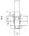
- FIG. 4 is a schematic diagram illustrating a horizontal cross-sectional view according to the embodiment of the magnetic memory element illustrated in FIG. 3 .
- FIG. 5 is a schematic diagram of a vertical cross-sectional view illustrating another embodiment of a magnetic memory element of the invention.
- FIGS. 1 and 2 illustrate one embodiment of a magnetic memory element, generally at 1 .
- the magnetic memory element 1 comprises a magnetic storage element 4 consisting of two magnetic layers 2 and 3 , which are made up of a ferromagnetic material, which may be conductive or not. Both magnetic layers 2 , 3 are positioned in intimate contact to the bit line (BL) on opposite sides of it in a parallel relationship, that is to say the bit line is sandwiched in between both magnetic layers 2 , 3 .
- Each of the magnetic layers 2 , 3 is in a vertical orientation relative to the surface of a wafer 19 on which the magnetic memory element is formed, and is provided with magnetic shape anisotropy, by appropriately choosing its aspect ratio, such that its height, i.e., dimension in a direction perpendicular to the wafer 19 surface, is slightly larger than its width, i.e., its dimension in a direction parallel to the wafer 19 surface, and is chosen to be larger than 1 and especially in the range of 1,5 to 3, and especially amount to approximately 2.
- the shape anisotropy of both magnetic layers 2 , 3 thus is perpendicularly oriented to the wafer 19 surface.
- magnetization vectors 5 , 6 of both magnetic layers 2 , 3 may be switched between the two directions perpendicularly aligned to the wafer 4 surface in response to external magnetic fields coupled therewith.
- the magnetization vectors 5 , 6 of both magnetic layers 2 , 3 are in an anti-parallel relationship, illustrated in FIG. 2 , both of which thus forming a flux-closed pair, so that magnetic interference between adjacent magnetic storage elements may be avoided.
- the magnetic layers 2 , 3 more precisely its magnetization vectors 5 , 6 are magnetically coupled to the magnetic field of the BL and to the magnetic field of a write word line (WWL) arranged underneath of it.
- WWL write word line
- the WWL creates a magnetic field 7 in the planes of the magnetic layers 2 , 3 of the magnetic storage element, while the BL creates a magnetic field (not shown in the figures) substantially perpendicular to the planes of the magnetic layers 2 , 3 of the magnetic storage element.
- both magnetization vectors 5 , 6 typically the Stoner-Wohlfahrt switching scenario may be used with the WWL underneath the magnetic layers 2 , 3 that creates the hard axis field, which switching scenario is well-known to the skilled persons and therefore need not be explained in further details here.
- the magnetic memory element 1 further comprises a horizontal magnetic sensor element 8 as magnetic field sensor being arranged separately from the magnetic storage element for sensing magnetization of the magnetic storage element, which is conductively interposed between BL and a selection device (not illustrated) formed in wafer 4 by way of a series connection comprised in that order of a via 12 , which is connected to the BL and magnetic sensor element 8 and for example is made of TaN, the magnetic sensor element 8 itself, a conductive layer 13 for a lateral shift of the series connection, which for example is made of TaN, and further vias 13 , 15 , for example made of TaN, the latter being connected to the selection device.
- magnetic sensor element 8 is magnetically coupled to the magnetic layers 2 , 3 of the magnetic storage element.
- the magnetic sensor element is realized as a magnetic tunnel junction (MTJ) having an aspect ratio of about 1, which comprises two ferromagnetic layers 9 and 10 of magnetic material stacked in parallel, overlying relationship and are separated by a layer of nonmagnetic material 11 .
- MTJ magnetic tunnel junction
- ferromagnetic layer 10 is designed to be a reference layer, the magnetic moment 17 of which being pinned, while the ferromagnetic layer 9 is designed to be a free layer, the magnetic moment 16 of which being free to be switched between the same and opposite directions with respect to the pinned magnetization direction of the reference layer.
- the orientation of the magnetic moment of the free layer thus may be switched between its parallel and anti-parallel states, in response to the magnetic stray field 18 of the magnetic layers 2 , 3 of the magnetic storage element, which is seen by the MTJ. Due to an aspect ratio of about 1, magnetic moment 16 of the free layer can be switched between its parallel and anti-parallel states according to the stray field 18 associated with different orientations of magnetization vectors 5 , 6 of the magnetic layers 2 , 3 of the magnetic storage element.
- a sense current which flows between BL and selection device. Reading out parallel and anti-parallel states of the MTJ, a read word line (RWL) is provided for.
- FIGS. 3 to 5 second and third embodiments of the magnetic memory element of the invention are explained.
- the differences to the above-described first embodiment will be explained, while otherwise reference is made to the explanations made relating to the first embodiment.
- FIGS. 3 and 4 illustrating a schematic vertical cross-sectional view and a schematic horizontal cross-sectional view, respectively, of a second embodiment of the magnetic memory element of the invention.
- the MTJ 8 is arranged to have a straight vertical electrical contact to the selection device, which in the second embodiment is realized as a FET-transistor 30 having source 21 and drain 20 .
- Electrical contact between MTJ 8 and drain 20 is realized by vias 22 , 23 and 24 , the first one being in electrical contact with BL in the first metallization (M 1 ), while the latter one being in contact with drain 20 .
- Such arrangement is advantageous in that the lateral dimension of the memory element size may be reduced to a minimum.
- the WWL has been arranged above MTJ 8 corresponding to a second metallization (M 2 ).
- a magnetic memory element (unit cell) 29 in FET architecture is illustrated (dashed).
- FET transistor 30 comprising source 21 and drain 20 contact is illustrated (dashed).
- the unit cell may be realized in about 4 F length and about 2 F width, thus resulting in a 8 F 2 structure, while the magnetic storage element 4 can be substantially wider than 1 F without increasing the cell size, independent of the size of the MTJ 8 , which can be kept at 1 F 2 .
- FIG. 5 illustrating a schematic vertical cross-sectional view along the bit line of a third embodiment of the magnetic memory element of the invention.
- the MTJ 8 is arranged to have a straight vertical electrical contact to the selection device.
- the selection device is realized as 4 F 2 diode cell 25 comprised of P + -layer 26 , N ⁇ -layer 27 and N + -layer 28 .
- N + -layer 28 may be identified as RWL.
- magnetic memory element 1 comprises a magnetic storage element and a magnetic sensor element, which may be provided in spatial distance from the magnetic storage element or be in contact therewith, and at least one current line, typically a number of three, which may be identified by a bit line, a write word line and read word line, respectively.
- the magnetic memory element 1 of the present invention is formed on a wafer surface.
- the magnetic storage element of the magnetic memory element 1 of the invention comprises at least one magnetic layer, which is made of a (ferro-) magnetic material, such as Ni, Fe, Co and their alloys, and is vertically oriented relative to the wafer surface on which the magnetic memory element is formed.
- This magnetic layer of the magnetic storage element is provided with magnetic anisotropy, which may be realized by appropriately choosing its aspect ratio and/or by intrinsic anisotropy, as is well-known to those skilled in the art.
- the height of the magnetic layer of the magnetic storage element may be chosen to be slightly larger than its width so as to give the magnetic layer a finite aspect ratio in vertical direction and thus shape anisotropy with a preferred direction perpendicular to the wafer surface.
- Intrinsic magnetic anisotropy may be combined with magnetic shape anisotropy.
- the magnetization vector of the magnetic layer of the magnetic storage element is magnetically coupled to the at least one current line, and, in a typical and preferable arrangement of the invention, is magnetically coupled to two current lines, which may be identified by the bit line and the (write) word line, respectively.
- the magnetization vector of the magnetic layer of the magnetic storage element in accordance with its magnetic anisotropy, is preferably oriented substantially perpendicular relative to the wafer surface.
- the former is preferably positioned adjacent or at least close to said at least one current line, which typically and preferably may be identified by the bit line. It especially may be advantageous if said magnetic storage element is positioned to be in contact with said at least one current line.
- the magnetic storage element comprises two magnetic layers 2 , 3 , which are positioned to be on opposite sides of said at least one current line (e.g., bit line) in a parallel relationship.
- said at least one current line e.g., bit line
- the magnetization vectors of both magnetic layers 2 , 3 of the magnetic storage element constituting a magnetic flux closed pair necessarily are in an anti-parallel magnetization configuration.
- the magnetic sensor element of the magnetic memory element 1 of the invention comprises at least one magnetic layer, made of a magnetic material, the magnetization vector of which being magnetically coupled to the magnetization vector of the at least one magnetic layer of the magnetic storage element.
- Magnetic coupling between the at least one magnetic layer of the magnetic storage element and the magnetic sensor element may be realized via a magnetic stray field of the at least one magnetic layer of the magnetic storage element seen by the magnetic sensor element.
- the magnetic sensor element in order to provide for sufficient magnetic coupling between magnetic storage and magnetic sensor elements, the magnetic sensor element has to be positioned within the magnetic stray field of the magnetic storage element, such that the magnetization vector of the magnetic layer of the magnetic sensor element may be sufficiently influenced, and particularly is able to follow the magnetization vector of the at least one magnetic layer of the magnetic storage element.
- the magnetic sensor element typically is placed in the vicinity of the magnetic storage element.
- magnetic coupling between the at least one magnetic layer of the magnetic storage element and the magnetic sensor element may also be realized via magnetic exchange coupling, in which case the magnetic storage element and the magnetic sensor element are brought into contact.
- the at least one magnetic layer of the magnetic sensor element is provided with magnetic anisotropy with its magnetization to be free to be switched between parallel and anti-parallel directions with respect to the direction of the magnetic anisotropy.
- Parallel and anti-parallel directions of the magnetization of the at least one magnetic layer of the magnetic sensor element preferably are associated with different electric resistance values exhibited by the magnetic sensor element.
- the magnetic sensor element of the magnetic memory element 1 of the invention is conductively connected to the at least one current line.
- it may be conductively connected to an active structure, that is to say a selection device of the wafer, like a FET-transistor, diode and the like.
- a selection device of the wafer like a FET-transistor, diode and the like.
- it may also be conductively connected to two current lines, wherein the first one of which may typically be identified as bit line, while the other one may typically be identified as word line.
- the magnetic sensor element preferably is realized as a magnetic tunnel junction, which comprises two magnetic layers made of magnetic material stacked in parallel, overlying relationship and is separated by a layer of nonmagnetic material. More specifically, the magnetic moment of one ferromagnetic layer (“reference layer”) is magnetically fixed or pinned, while the magnetic moment of the other ferromagnetic layer (“free layer”) is free to be switched between the same and opposite directions with respect to the fixed magnetization direction of the reference layer. Depending upon the magnetic states of the free layer (i.e., parallel or anti-parallel states), the magnetic sensor element exhibits two different resistance values in response to a voltage applied across the magnetic tunnel junction barrier.
- reference layer the magnetic moment of one ferromagnetic layer
- free layer the magnetic moment of the other ferromagnetic layer
- the magnetic sensor element exhibits two different resistance values in response to a voltage applied across the magnetic tunnel junction barrier.
- the particular resistance of the magnetic sensor element thus reflects the magnetization state of the free layer in response to the sensed magnetization of the magnetic storage element magnetically coupled therewith, wherein resistance is “low” when the magnetization of the free layer is parallel to the magnetization of the reference layer, and “high” when the magnetization is anti-parallel. Accordingly, a detection of changes in resistance allows such magnetic sensor element to provide information stored in the magnetic storage element, that is to say, to read information from the magnetic storage element.
- the magnetic layer of the magnetic sensor element is substantially parallel to the wafer surface, that is to say the magnetic layer with its magnetization vector oriented in that plane is horizontally aligned.
- the magnetic sensor element of the magnetic memory element of the invention may be conductively interposed between the at least one current line, which may be identified as bit line, and a selection device. In other words, an electrical series connection comprising the at least one current line, magnetic sensor element and selection device in that order is established.
- the magnetic sensor element of the magnetic memory element of the invention may be conductively interposed between two current lines, which may be identified as bit line and word line, respectively, In other words, an electrical series connection comprising bit line, magnetic sensor element and word line in that order is established.
- the magnetic sensor element of the invention can have an arbitrarily chosen shape, for instance circle, round, square with rounded edges and the like.
- the magnetic storage element is arranged above the magnetic sensor element.
- the magnetic sensor element in view of magnetic coupling between magnetic storage element and current lines, it may be advantageous to arrange the magnetic sensor element in between a first current line, which typically may be identified by a bit line, and a second current line, which typically may be identified by a write word line.
- the magnetic sensor element is arranged to have a straight vertical electrical contact to the selection device, or alternatively (in cross-point architecture) the current line, which straight vertical electrical contact may typically be realized by an electrical via, that is to say a via filled with conductive material.
- the first current line which typically may be identified by a bit line, in between two layers of the magnetic storage element, while a second current line is provided vertically above the magnetic storage element.
- an aspect ratio of the at least one magnetic layer of the magnetic storage element preferably is chosen to be larger than 1, and may particularly be in the range of from 1.5 to 3 in order to provide for a sufficiently high magnetic shape anisotropy.
- the magnetic anisotropy of the magnetic layer of the magnetic sensor element has to be chosen to be smaller than that one of the at least one magnetic layer of the magnetic storage element. While, basically, shape anisotropy may be combined with intrinsic anistropy, i.e., shape anisotropy may be (partially) compensated or added by intrinsic anisotropy, it is clear that it is the resulting total magnetic anisotropy that has to be chosen to be smaller than that one of the at least one magnetic layer of the magnetic storage element. To this aim, it may be preferable to choose an aspect ratio of the magnetic layer of the magnetic sensor element, which is in the range of from 1 to 2, and more preferably amounts to approximately 1.
- such memory element may be realized in approximately 8 F 2 structure size, wherein F is the minimum lithographic feature size, which at present using (UV) photolithographic methods amounts to about 90 nm. Otherwise, independently from the size of the magnetic memory element as such, the magnetic sensor element may preferably be realized in about 1 F 2 structure size.
- the magnetic random access memory device comprises a plurality of magnetic memory elements as above-described.
- the magnetic random access memory device comprises a plurality of first current lines and plurality of second current lines, wherein each of the magnetic memory elements is magnetically coupled to one of the first current lines and one of the second current lines.
- each of the magnetic sensor elements of the magnetic memory elements may be conductively interposed between the one of the first and second current lines and a selection device.
- each of the magnetic sensor elements of the magnetic memory elements may be conductively interposed between the one of said first current lines and the one of said second current lines.
- the term “aspect ratio” denotes a ratio of orthogonal dimensions which span the magnetization vector's plane, which in a vertically oriented plane may be identified by a ratio of its height to its width, and in a horizontally oriented plane may be identified by a ratio of its length to its width.
- the term “vertical” relates to the plane of the wafer surface and thus denotes a direction perpendicularly oriented to the wafer surface
- the term “horizontal” denotes a direction parallelly oriented to the wafer surface.
- magnetic memory element 1 With the above magnetic memory element 1 , and in contrast to conventional MRAM-cells where magnetic storage element and magnetic field sensor are both incorporated in the free layer of one and the same magnetic tunneling junction, it is possible to store information in the magnetic polarization of the magnetic storage element, while the readout is done in a separate magnetic sensor element, for example a magnetic tunneling junction, which may be spatially distanced from the magnetic storage element or be in contact therewith. Since the magnetic sensor element, which just serves as field sensor, is separated from the magnetic storage element, it can be realized arbitrarily small. Contrary to the magnetic storage element being vertically oriented, the magnetic sensor element can be horizontally oriented and, thus, can be produced with conventional thin layer deposition and patterning technology.
- the horizontal magnetic sensor element can be made very small and have an aspect ratio of about 1. It, however, should have a lower magnetic anisotropy than the magnetic storage element to follow the magnetic field arising from the vertical magnetic storage element. Otherwise, the aspect ratio and thus the switching field (in case that shape anisotropy is used) of the vertically aligned magnetic storage element can be controlled by the depth of the trench to be etched for its realization.
- the actual magnetic storage element can be made rather large, in particular with a large enough volume to prevent thermally activated switching.
- the magnetic sensor element for sensing the magnetic stray field of the magnetic storage element its activation energy is given by the Zeeman energy difference 2HM S V, where H is the magnetic stray field from the magnetic storage element seen by the magnetic sensor element, M S is its saturation magnetization, and V the volume of its free layer.
- H the magnetic stray field from the magnetic storage element seen by the magnetic sensor element
- M S is its saturation magnetization
- V the volume of its free layer.
- the whole structure of the magnetic storage element which may be comprised of two magnetic layers, and the magnetic sensor element can be optimized as a whole in terms of switching fields and activation energy to the lowest lying erroneous state.
- the interaction between magnetic storage elements is strongly reduced as first of all the magnetic field points mostly perpendicular to the wafer surface, provided that the magnetic anisotropy is perpendicularly oriented to the wafer surface, and may also be very well flux-closed.
- the magnetic sensor elements their magnetic moments and thus interaction is very small as they may be realized to have only a small total magnetic moment, due to an aspect ratio near 1.
- the vertical magnetic storage element can be made substantially wider than 1 F without increasing the magnetic memory element size, independent of the size of the actual planar, horizontal magnetic memory element which can be kept at 1 F 2 .
- the magnetic sensor element can be made easily 180 nm wide or more (and e.g., 360 nm deep, 5 nm thick, i.e., about the size of a nowadays 180 nm technology cell), as the unit memory cell has at best 4 F in the long direction (assuming DRAM technology transistors with basically no contact overhead).
- 2 F 180 nm between neighboring magnetic memory elements on the same bit line.
- the spacing of the magnetic storage elements is less critical than for planar elements, as they do not interact unless written (the magnetization vector is perpendicular to the wafer plane).
- the length of the memory unit cell possibly shrinks to 3 F (again assuming zero overhead for contacts), and so a 2 F vertical magnetic storage element has still 1 F spacing.
- the magnetic storage elements of the magnetic memory elements of the invention can be produced with the regular liner process plus an additional patterning in a first current line (e.g., bit line) direction.
- a first current line e.g., bit line
- This can be done by patterning the liner before filling the trench with a conductive material such as copper.
- a conductive material such as copper.
- the liner patterning should be done after etching out the bottom, so that only the side walls remain.
Abstract
Description
Claims (25)
Priority Applications (2)
| Application Number | Priority Date | Filing Date | Title |
|---|---|---|---|
| US10/923,651 US7200032B2 (en) | 2004-08-20 | 2004-08-20 | MRAM with vertical storage element and field sensor |
| DE102005035164A DE102005035164A1 (en) | 2004-08-20 | 2005-07-27 | MRAM with vertical storage element and field sensor |
Applications Claiming Priority (1)
| Application Number | Priority Date | Filing Date | Title |
|---|---|---|---|
| US10/923,651 US7200032B2 (en) | 2004-08-20 | 2004-08-20 | MRAM with vertical storage element and field sensor |
Publications (2)
| Publication Number | Publication Date |
|---|---|
| US20060039187A1 US20060039187A1 (en) | 2006-02-23 |
| US7200032B2 true US7200032B2 (en) | 2007-04-03 |
Family
ID=35745823
Family Applications (1)
| Application Number | Title | Priority Date | Filing Date |
|---|---|---|---|
| US10/923,651 Expired - Fee Related US7200032B2 (en) | 2004-08-20 | 2004-08-20 | MRAM with vertical storage element and field sensor |
Country Status (2)
| Country | Link |
|---|---|
| US (1) | US7200032B2 (en) |
| DE (1) | DE102005035164A1 (en) |
Cited By (4)
| Publication number | Priority date | Publication date | Assignee | Title |
|---|---|---|---|---|
| US20060098479A1 (en) * | 2003-11-10 | 2006-05-11 | Santosh Kumar | CMI-001U solid state magnetic memory system and method |
| US20060256609A1 (en) * | 2003-03-31 | 2006-11-16 | Matsushita Electric Industrial Co., Ltd. | Memory cell, memory using the memory cell, memory cell manuracturing method, and memory recording/reading method |
| US20070279978A1 (en) * | 2006-05-30 | 2007-12-06 | Macronix International Co., Ltd. | Magnetic random access memory using single crystal self-aligned diode |
| US20100103720A1 (en) * | 2002-12-21 | 2010-04-29 | Hynix Semiconductor Inc. | Biosensor and sensing cell array using the same |
Families Citing this family (4)
| Publication number | Priority date | Publication date | Assignee | Title |
|---|---|---|---|---|
| DE102006046499B4 (en) * | 2006-09-29 | 2011-05-05 | Siemens Ag | information store |
| US20140026659A1 (en) * | 2012-07-27 | 2014-01-30 | Biao Zhang | Mems device and a method of using the same |
| US9842986B2 (en) * | 2015-12-15 | 2017-12-12 | Taiwan Semiconductor Manufacturing Company Ltd. | Semiconductor structure and method of forming the same |
| US10529400B1 (en) * | 2018-07-27 | 2020-01-07 | Nxp Usa, Inc. | Magnetic attack detection in a magnetic random access memory (MRAM) |
Citations (12)
| Publication number | Priority date | Publication date | Assignee | Title |
|---|---|---|---|---|
| DE1387400U (en) | ||||
| US6545906B1 (en) | 2001-10-16 | 2003-04-08 | Motorola, Inc. | Method of writing to scalable magnetoresistance random access memory element |
| US20030137870A1 (en) | 2000-07-27 | 2003-07-24 | Yoshiaki Saito | Magnetic memory |
| US6664579B2 (en) * | 2001-05-22 | 2003-12-16 | Hynix Semiconductor Inc. | Magnetic random access memory using bipolar junction transistor |
| US20040037109A1 (en) | 2002-08-21 | 2004-02-26 | Witcraft William F. | Method for building a magnetic keeper or flux concentrator used for writing magnetic bits on a MRAM device |
| US20040057295A1 (en) | 2001-01-19 | 2004-03-25 | Nozomu Matsukawa | Magnetic storage element, production method and driving method therefor, and memory array |
| US20040057303A1 (en) | 2001-12-05 | 2004-03-25 | Darrel Bloomquist | Method and article for concentrating fields at sense |
| US6803619B2 (en) * | 2002-07-10 | 2004-10-12 | Kabushiki Kaisha Toshiba | Semiconductor memory device |
| US6909630B2 (en) * | 2002-12-09 | 2005-06-21 | Applied Spintronics Technology, Inc. | MRAM memories utilizing magnetic write lines |
| US20060039185A1 (en) * | 2004-08-20 | 2006-02-23 | Daniel Braun | MRAM with magnetic via for storage of information and field sensor |
| US20060039186A1 (en) * | 2004-08-20 | 2006-02-23 | Daniel Braun | MRAM with vertical storage element in two layer-arrangement and field sensor |
| DE102005034665A1 (en) | 2004-07-26 | 2006-03-23 | Infineon Technologies Ag | Ferromagnetic liners for printed circuit traces of magnetic memory cells and method for producing the same |
-
2004
- 2004-08-20 US US10/923,651 patent/US7200032B2/en not_active Expired - Fee Related
-
2005
- 2005-07-27 DE DE102005035164A patent/DE102005035164A1/en not_active Withdrawn
Patent Citations (13)
| Publication number | Priority date | Publication date | Assignee | Title |
|---|---|---|---|---|
| DE1387400U (en) | ||||
| US20030137870A1 (en) | 2000-07-27 | 2003-07-24 | Yoshiaki Saito | Magnetic memory |
| US20040057295A1 (en) | 2001-01-19 | 2004-03-25 | Nozomu Matsukawa | Magnetic storage element, production method and driving method therefor, and memory array |
| US6664579B2 (en) * | 2001-05-22 | 2003-12-16 | Hynix Semiconductor Inc. | Magnetic random access memory using bipolar junction transistor |
| US6545906B1 (en) | 2001-10-16 | 2003-04-08 | Motorola, Inc. | Method of writing to scalable magnetoresistance random access memory element |
| US20040057303A1 (en) | 2001-12-05 | 2004-03-25 | Darrel Bloomquist | Method and article for concentrating fields at sense |
| US6803619B2 (en) * | 2002-07-10 | 2004-10-12 | Kabushiki Kaisha Toshiba | Semiconductor memory device |
| US20040037109A1 (en) | 2002-08-21 | 2004-02-26 | Witcraft William F. | Method for building a magnetic keeper or flux concentrator used for writing magnetic bits on a MRAM device |
| US6909630B2 (en) * | 2002-12-09 | 2005-06-21 | Applied Spintronics Technology, Inc. | MRAM memories utilizing magnetic write lines |
| DE102005034665A1 (en) | 2004-07-26 | 2006-03-23 | Infineon Technologies Ag | Ferromagnetic liners for printed circuit traces of magnetic memory cells and method for producing the same |
| US20060039185A1 (en) * | 2004-08-20 | 2006-02-23 | Daniel Braun | MRAM with magnetic via for storage of information and field sensor |
| US20060039186A1 (en) * | 2004-08-20 | 2006-02-23 | Daniel Braun | MRAM with vertical storage element in two layer-arrangement and field sensor |
| US7092284B2 (en) * | 2004-08-20 | 2006-08-15 | Infineon Technologies Ag | MRAM with magnetic via for storage of information and field sensor |
Non-Patent Citations (1)
| Title |
|---|
| German Office Action dated Aug. 14, 2006. (4 pgs.). |
Cited By (8)
| Publication number | Priority date | Publication date | Assignee | Title |
|---|---|---|---|---|
| US20100103720A1 (en) * | 2002-12-21 | 2010-04-29 | Hynix Semiconductor Inc. | Biosensor and sensing cell array using the same |
| US8174879B2 (en) * | 2002-12-21 | 2012-05-08 | Hynix Semiconductor Inc. | Biosensor and sensing cell array using the same |
| US20060256609A1 (en) * | 2003-03-31 | 2006-11-16 | Matsushita Electric Industrial Co., Ltd. | Memory cell, memory using the memory cell, memory cell manuracturing method, and memory recording/reading method |
| US7436697B2 (en) * | 2003-03-31 | 2008-10-14 | Matsushita Electric Industrial Co., Ltd. | Memory cell, memory using the memory cell, memory cell manufacturing method, and memory recording/reading method |
| US20060098479A1 (en) * | 2003-11-10 | 2006-05-11 | Santosh Kumar | CMI-001U solid state magnetic memory system and method |
| US7394683B2 (en) * | 2003-11-10 | 2008-07-01 | Magsil Corporation, Inc. | Solid state magnetic memory system and method |
| US20070279978A1 (en) * | 2006-05-30 | 2007-12-06 | Macronix International Co., Ltd. | Magnetic random access memory using single crystal self-aligned diode |
| US7728384B2 (en) * | 2006-05-30 | 2010-06-01 | Macronix International Co., Ltd. | Magnetic random access memory using single crystal self-aligned diode |
Also Published As
| Publication number | Publication date |
|---|---|
| US20060039187A1 (en) | 2006-02-23 |
| DE102005035164A1 (en) | 2006-03-02 |
Similar Documents
| Publication | Publication Date | Title |
|---|---|---|
| US7092284B2 (en) | MRAM with magnetic via for storage of information and field sensor | |
| US8120950B2 (en) | Semiconductor device | |
| US7212432B2 (en) | Resistive memory cell random access memory device and method of fabrication | |
| US9129893B2 (en) | Semiconductor device | |
| US10242725B2 (en) | Modular magnetoresistive memory | |
| KR20180022540A (en) | Zero transistor transverse current bi-directional bitcell | |
| EP2124228B1 (en) | Magnetic random access memory with an elliptical junction | |
| US6958246B2 (en) | Methods of forming magnetoresistive memory devices | |
| EP1398789B1 (en) | Magnetic random access memory with soft magnetic reference layers | |
| US7068533B2 (en) | Resistive memory cell configuration and method for sensing resistance values | |
| US6882563B2 (en) | Magnetic memory device and method for manufacturing the same | |
| KR20070027635A (en) | Reversed magnetic tunneling junction for power efficient byte writing of mram | |
| US7200032B2 (en) | MRAM with vertical storage element and field sensor | |
| US7075807B2 (en) | Magnetic memory with static magnetic offset field | |
| US7088612B2 (en) | MRAM with vertical storage element in two layer-arrangement and field sensor | |
| JP2005191523A (en) | Magnetic ram | |
| EP1634298B1 (en) | Cross-point mram array with reduced voltage drop across mtj's | |
| KR100422945B1 (en) | A method for writing of a magnetic random access memory using bipolar junction transistor | |
| US7061795B2 (en) | Magnetic random access memory device | |
| JP4150047B2 (en) | Magnetic storage | |
| TWI833221B (en) | Magnetic memory device | |
| JP4068337B2 (en) | Magnetic random access memory | |
| JP2005183825A (en) | Magnetic memory | |
| TW202312525A (en) | Magnetic memory device | |
| JP2008085349A (en) | Magnetic random access memory |
Legal Events
| Date | Code | Title | Description |
|---|---|---|---|
| AS | Assignment |
Owner name: ATLIS SEMICONDUCTOR, FRANCE Free format text: ASSIGNMENT OF ASSIGNORS INTEREST;ASSIGNORS:BRAUN, DANIEL;FERRANT, RICHARD;REEL/FRAME:015588/0773 Effective date: 20041102 |
|
| AS | Assignment |
Owner name: ALTIS SEMICONDUCTOR, FRANCE Free format text: ASSIGNMENT OF ASSIGNORS INTEREST;ASSIGNORS:BRAUN, DANIEL;FERRANT, RICHARD;REEL/FRAME:015968/0238;SIGNING DATES FROM 20050205 TO 20050310 Owner name: INFINEON TECHNOLOGIES AG, GERMANY Free format text: ASSIGNMENT OF ASSIGNORS INTEREST;ASSIGNORS:BRAUN, DANIEL;FERRANT, RICHARD;REEL/FRAME:015968/0238;SIGNING DATES FROM 20050205 TO 20050310 |
|
| FEPP | Fee payment procedure |
Free format text: PAYOR NUMBER ASSIGNED (ORIGINAL EVENT CODE: ASPN); ENTITY STATUS OF PATENT OWNER: LARGE ENTITY |
|
| STCF | Information on status: patent grant |
Free format text: PATENTED CASE |
|
| AS | Assignment |
Owner name: QIMONDA AG, GERMANY Free format text: ASSIGNMENT OF ASSIGNORS INTEREST;ASSIGNOR:INFINEON TECHNOLOGIES AG;REEL/FRAME:023821/0535 Effective date: 20060425 Owner name: QIMONDA AG,GERMANY Free format text: ASSIGNMENT OF ASSIGNORS INTEREST;ASSIGNOR:INFINEON TECHNOLOGIES AG;REEL/FRAME:023821/0535 Effective date: 20060425 |
|
| REMI | Maintenance fee reminder mailed | ||
| FPAY | Fee payment |
Year of fee payment: 4 |
|
| SULP | Surcharge for late payment | ||
| FPAY | Fee payment |
Year of fee payment: 8 |
|
| AS | Assignment |
Owner name: INFINEON TECHNOLOGIES AG, GERMANY Free format text: ASSIGNMENT OF ASSIGNORS INTEREST;ASSIGNOR:QIMONDA AG;REEL/FRAME:035623/0001 Effective date: 20141009 |
|
| FEPP | Fee payment procedure |
Free format text: MAINTENANCE FEE REMINDER MAILED (ORIGINAL EVENT CODE: REM.); ENTITY STATUS OF PATENT OWNER: LARGE ENTITY |
|
| LAPS | Lapse for failure to pay maintenance fees |
Free format text: PATENT EXPIRED FOR FAILURE TO PAY MAINTENANCE FEES (ORIGINAL EVENT CODE: EXP.); ENTITY STATUS OF PATENT OWNER: LARGE ENTITY |
|
| STCH | Information on status: patent discontinuation |
Free format text: PATENT EXPIRED DUE TO NONPAYMENT OF MAINTENANCE FEES UNDER 37 CFR 1.362 |
|
| FP | Lapsed due to failure to pay maintenance fee |
Effective date: 20190403 |