US7173341B2 - High performance thermally enhanced package and method of fabricating the same - Google Patents
High performance thermally enhanced package and method of fabricating the same Download PDFInfo
- Publication number
- US7173341B2 US7173341B2 US10/368,337 US36833703A US7173341B2 US 7173341 B2 US7173341 B2 US 7173341B2 US 36833703 A US36833703 A US 36833703A US 7173341 B2 US7173341 B2 US 7173341B2
- Authority
- US
- United States
- Prior art keywords
- chip
- package
- carrier
- heat sink
- cavity
- Prior art date
- Legal status (The legal status is an assumption and is not a legal conclusion. Google has not performed a legal analysis and makes no representation as to the accuracy of the status listed.)
- Expired - Lifetime, expires
Links
- 238000004519 manufacturing process Methods 0.000 title abstract description 8
- 239000000853 adhesive Substances 0.000 claims description 44
- 230000001070 adhesive effect Effects 0.000 claims description 44
- 239000003292 glue Substances 0.000 claims description 44
- 239000007787 solid Substances 0.000 claims description 6
- 238000007906 compression Methods 0.000 abstract description 7
- 230000006835 compression Effects 0.000 abstract description 4
- 238000000465 moulding Methods 0.000 abstract description 3
- 238000005516 engineering process Methods 0.000 abstract description 2
- 150000001875 compounds Chemical class 0.000 abstract 1
- PCHJSUWPFVWCPO-UHFFFAOYSA-N gold Chemical compound [Au] PCHJSUWPFVWCPO-UHFFFAOYSA-N 0.000 description 16
- 239000010931 gold Substances 0.000 description 16
- 229910052737 gold Inorganic materials 0.000 description 16
- 238000000034 method Methods 0.000 description 11
- 230000008569 process Effects 0.000 description 9
- 229910000679 solder Inorganic materials 0.000 description 7
- 238000004806 packaging method and process Methods 0.000 description 5
- XUIMIQQOPSSXEZ-UHFFFAOYSA-N Silicon Chemical compound [Si] XUIMIQQOPSSXEZ-UHFFFAOYSA-N 0.000 description 4
- 238000009713 electroplating Methods 0.000 description 4
- 239000000463 material Substances 0.000 description 4
- 229910052710 silicon Inorganic materials 0.000 description 4
- 239000010703 silicon Substances 0.000 description 4
- 230000008901 benefit Effects 0.000 description 3
- 238000005538 encapsulation Methods 0.000 description 2
- 238000012986 modification Methods 0.000 description 2
- 230000004048 modification Effects 0.000 description 2
- 230000003071 parasitic effect Effects 0.000 description 2
- 239000004065 semiconductor Substances 0.000 description 2
- 239000000969 carrier Substances 0.000 description 1
- 230000000295 complement effect Effects 0.000 description 1
- 238000000280 densification Methods 0.000 description 1
- 238000005530 etching Methods 0.000 description 1
- 230000017525 heat dissipation Effects 0.000 description 1
- 239000011796 hollow space material Substances 0.000 description 1
- 230000006698 induction Effects 0.000 description 1
- 230000006855 networking Effects 0.000 description 1
- 238000012858 packaging process Methods 0.000 description 1
- 238000004904 shortening Methods 0.000 description 1
- 238000005476 soldering Methods 0.000 description 1
Images


Classifications
-
- H—ELECTRICITY
- H01—ELECTRIC ELEMENTS
- H01L—SEMICONDUCTOR DEVICES NOT COVERED BY CLASS H10
- H01L23/00—Details of semiconductor or other solid state devices
- H01L23/48—Arrangements for conducting electric current to or from the solid state body in operation, e.g. leads, terminal arrangements ; Selection of materials therefor
- H01L23/488—Arrangements for conducting electric current to or from the solid state body in operation, e.g. leads, terminal arrangements ; Selection of materials therefor consisting of soldered or bonded constructions
- H01L23/495—Lead-frames or other flat leads
- H01L23/49572—Lead-frames or other flat leads consisting of thin flexible metallic tape with or without a film carrier
-
- H—ELECTRICITY
- H01—ELECTRIC ELEMENTS
- H01L—SEMICONDUCTOR DEVICES NOT COVERED BY CLASS H10
- H01L23/00—Details of semiconductor or other solid state devices
- H01L23/16—Fillings or auxiliary members in containers or encapsulations, e.g. centering rings
- H01L23/18—Fillings characterised by the material, its physical or chemical properties, or its arrangement within the complete device
- H01L23/24—Fillings characterised by the material, its physical or chemical properties, or its arrangement within the complete device solid or gel at the normal operating temperature of the device
-
- H—ELECTRICITY
- H01—ELECTRIC ELEMENTS
- H01L—SEMICONDUCTOR DEVICES NOT COVERED BY CLASS H10
- H01L23/00—Details of semiconductor or other solid state devices
- H01L23/34—Arrangements for cooling, heating, ventilating or temperature compensation ; Temperature sensing arrangements
- H01L23/36—Selection of materials, or shaping, to facilitate cooling or heating, e.g. heatsinks
-
- H—ELECTRICITY
- H01—ELECTRIC ELEMENTS
- H01L—SEMICONDUCTOR DEVICES NOT COVERED BY CLASS H10
- H01L2224/00—Indexing scheme for arrangements for connecting or disconnecting semiconductor or solid-state bodies and methods related thereto as covered by H01L24/00
- H01L2224/01—Means for bonding being attached to, or being formed on, the surface to be connected, e.g. chip-to-package, die-attach, "first-level" interconnects; Manufacturing methods related thereto
- H01L2224/26—Layer connectors, e.g. plate connectors, solder or adhesive layers; Manufacturing methods related thereto
- H01L2224/31—Structure, shape, material or disposition of the layer connectors after the connecting process
- H01L2224/32—Structure, shape, material or disposition of the layer connectors after the connecting process of an individual layer connector
- H01L2224/321—Disposition
- H01L2224/32151—Disposition the layer connector connecting between a semiconductor or solid-state body and an item not being a semiconductor or solid-state body, e.g. chip-to-substrate, chip-to-passive
- H01L2224/32221—Disposition the layer connector connecting between a semiconductor or solid-state body and an item not being a semiconductor or solid-state body, e.g. chip-to-substrate, chip-to-passive the body and the item being stacked
- H01L2224/32245—Disposition the layer connector connecting between a semiconductor or solid-state body and an item not being a semiconductor or solid-state body, e.g. chip-to-substrate, chip-to-passive the body and the item being stacked the item being metallic
-
- H—ELECTRICITY
- H01—ELECTRIC ELEMENTS
- H01L—SEMICONDUCTOR DEVICES NOT COVERED BY CLASS H10
- H01L2224/00—Indexing scheme for arrangements for connecting or disconnecting semiconductor or solid-state bodies and methods related thereto as covered by H01L24/00
- H01L2224/01—Means for bonding being attached to, or being formed on, the surface to be connected, e.g. chip-to-package, die-attach, "first-level" interconnects; Manufacturing methods related thereto
- H01L2224/42—Wire connectors; Manufacturing methods related thereto
- H01L2224/44—Structure, shape, material or disposition of the wire connectors prior to the connecting process
- H01L2224/45—Structure, shape, material or disposition of the wire connectors prior to the connecting process of an individual wire connector
- H01L2224/45001—Core members of the connector
- H01L2224/45099—Material
- H01L2224/451—Material with a principal constituent of the material being a metal or a metalloid, e.g. boron (B), silicon (Si), germanium (Ge), arsenic (As), antimony (Sb), tellurium (Te) and polonium (Po), and alloys thereof
- H01L2224/45138—Material with a principal constituent of the material being a metal or a metalloid, e.g. boron (B), silicon (Si), germanium (Ge), arsenic (As), antimony (Sb), tellurium (Te) and polonium (Po), and alloys thereof the principal constituent melting at a temperature of greater than or equal to 950°C and less than 1550°C
- H01L2224/45144—Gold (Au) as principal constituent
-
- H—ELECTRICITY
- H01—ELECTRIC ELEMENTS
- H01L—SEMICONDUCTOR DEVICES NOT COVERED BY CLASS H10
- H01L2224/00—Indexing scheme for arrangements for connecting or disconnecting semiconductor or solid-state bodies and methods related thereto as covered by H01L24/00
- H01L2224/01—Means for bonding being attached to, or being formed on, the surface to be connected, e.g. chip-to-package, die-attach, "first-level" interconnects; Manufacturing methods related thereto
- H01L2224/42—Wire connectors; Manufacturing methods related thereto
- H01L2224/47—Structure, shape, material or disposition of the wire connectors after the connecting process
- H01L2224/48—Structure, shape, material or disposition of the wire connectors after the connecting process of an individual wire connector
- H01L2224/4805—Shape
- H01L2224/4809—Loop shape
- H01L2224/48091—Arched
-
- H—ELECTRICITY
- H01—ELECTRIC ELEMENTS
- H01L—SEMICONDUCTOR DEVICES NOT COVERED BY CLASS H10
- H01L2224/00—Indexing scheme for arrangements for connecting or disconnecting semiconductor or solid-state bodies and methods related thereto as covered by H01L24/00
- H01L2224/01—Means for bonding being attached to, or being formed on, the surface to be connected, e.g. chip-to-package, die-attach, "first-level" interconnects; Manufacturing methods related thereto
- H01L2224/42—Wire connectors; Manufacturing methods related thereto
- H01L2224/47—Structure, shape, material or disposition of the wire connectors after the connecting process
- H01L2224/48—Structure, shape, material or disposition of the wire connectors after the connecting process of an individual wire connector
- H01L2224/481—Disposition
- H01L2224/48151—Connecting between a semiconductor or solid-state body and an item not being a semiconductor or solid-state body, e.g. chip-to-substrate, chip-to-passive
- H01L2224/48221—Connecting between a semiconductor or solid-state body and an item not being a semiconductor or solid-state body, e.g. chip-to-substrate, chip-to-passive the body and the item being stacked
- H01L2224/48245—Connecting between a semiconductor or solid-state body and an item not being a semiconductor or solid-state body, e.g. chip-to-substrate, chip-to-passive the body and the item being stacked the item being metallic
- H01L2224/48247—Connecting between a semiconductor or solid-state body and an item not being a semiconductor or solid-state body, e.g. chip-to-substrate, chip-to-passive the body and the item being stacked the item being metallic connecting the wire to a bond pad of the item
-
- H—ELECTRICITY
- H01—ELECTRIC ELEMENTS
- H01L—SEMICONDUCTOR DEVICES NOT COVERED BY CLASS H10
- H01L2224/00—Indexing scheme for arrangements for connecting or disconnecting semiconductor or solid-state bodies and methods related thereto as covered by H01L24/00
- H01L2224/01—Means for bonding being attached to, or being formed on, the surface to be connected, e.g. chip-to-package, die-attach, "first-level" interconnects; Manufacturing methods related thereto
- H01L2224/42—Wire connectors; Manufacturing methods related thereto
- H01L2224/47—Structure, shape, material or disposition of the wire connectors after the connecting process
- H01L2224/48—Structure, shape, material or disposition of the wire connectors after the connecting process of an individual wire connector
- H01L2224/481—Disposition
- H01L2224/48151—Connecting between a semiconductor or solid-state body and an item not being a semiconductor or solid-state body, e.g. chip-to-substrate, chip-to-passive
- H01L2224/48221—Connecting between a semiconductor or solid-state body and an item not being a semiconductor or solid-state body, e.g. chip-to-substrate, chip-to-passive the body and the item being stacked
- H01L2224/48245—Connecting between a semiconductor or solid-state body and an item not being a semiconductor or solid-state body, e.g. chip-to-substrate, chip-to-passive the body and the item being stacked the item being metallic
- H01L2224/48257—Connecting between a semiconductor or solid-state body and an item not being a semiconductor or solid-state body, e.g. chip-to-substrate, chip-to-passive the body and the item being stacked the item being metallic connecting the wire to a die pad of the item
-
- H—ELECTRICITY
- H01—ELECTRIC ELEMENTS
- H01L—SEMICONDUCTOR DEVICES NOT COVERED BY CLASS H10
- H01L2224/00—Indexing scheme for arrangements for connecting or disconnecting semiconductor or solid-state bodies and methods related thereto as covered by H01L24/00
- H01L2224/01—Means for bonding being attached to, or being formed on, the surface to be connected, e.g. chip-to-package, die-attach, "first-level" interconnects; Manufacturing methods related thereto
- H01L2224/42—Wire connectors; Manufacturing methods related thereto
- H01L2224/47—Structure, shape, material or disposition of the wire connectors after the connecting process
- H01L2224/48—Structure, shape, material or disposition of the wire connectors after the connecting process of an individual wire connector
- H01L2224/484—Connecting portions
- H01L2224/48463—Connecting portions the connecting portion on the bonding area of the semiconductor or solid-state body being a ball bond
-
- H—ELECTRICITY
- H01—ELECTRIC ELEMENTS
- H01L—SEMICONDUCTOR DEVICES NOT COVERED BY CLASS H10
- H01L2224/00—Indexing scheme for arrangements for connecting or disconnecting semiconductor or solid-state bodies and methods related thereto as covered by H01L24/00
- H01L2224/73—Means for bonding being of different types provided for in two or more of groups H01L2224/10, H01L2224/18, H01L2224/26, H01L2224/34, H01L2224/42, H01L2224/50, H01L2224/63, H01L2224/71
- H01L2224/732—Location after the connecting process
- H01L2224/73251—Location after the connecting process on different surfaces
- H01L2224/73265—Layer and wire connectors
-
- H—ELECTRICITY
- H01—ELECTRIC ELEMENTS
- H01L—SEMICONDUCTOR DEVICES NOT COVERED BY CLASS H10
- H01L24/00—Arrangements for connecting or disconnecting semiconductor or solid-state bodies; Methods or apparatus related thereto
- H01L24/01—Means for bonding being attached to, or being formed on, the surface to be connected, e.g. chip-to-package, die-attach, "first-level" interconnects; Manufacturing methods related thereto
- H01L24/42—Wire connectors; Manufacturing methods related thereto
- H01L24/44—Structure, shape, material or disposition of the wire connectors prior to the connecting process
- H01L24/45—Structure, shape, material or disposition of the wire connectors prior to the connecting process of an individual wire connector
-
- H—ELECTRICITY
- H01—ELECTRIC ELEMENTS
- H01L—SEMICONDUCTOR DEVICES NOT COVERED BY CLASS H10
- H01L24/00—Arrangements for connecting or disconnecting semiconductor or solid-state bodies; Methods or apparatus related thereto
- H01L24/01—Means for bonding being attached to, or being formed on, the surface to be connected, e.g. chip-to-package, die-attach, "first-level" interconnects; Manufacturing methods related thereto
- H01L24/42—Wire connectors; Manufacturing methods related thereto
- H01L24/47—Structure, shape, material or disposition of the wire connectors after the connecting process
- H01L24/48—Structure, shape, material or disposition of the wire connectors after the connecting process of an individual wire connector
-
- H—ELECTRICITY
- H01—ELECTRIC ELEMENTS
- H01L—SEMICONDUCTOR DEVICES NOT COVERED BY CLASS H10
- H01L2924/00—Indexing scheme for arrangements or methods for connecting or disconnecting semiconductor or solid-state bodies as covered by H01L24/00
- H01L2924/0001—Technical content checked by a classifier
- H01L2924/00014—Technical content checked by a classifier the subject-matter covered by the group, the symbol of which is combined with the symbol of this group, being disclosed without further technical details
-
- H—ELECTRICITY
- H01—ELECTRIC ELEMENTS
- H01L—SEMICONDUCTOR DEVICES NOT COVERED BY CLASS H10
- H01L2924/00—Indexing scheme for arrangements or methods for connecting or disconnecting semiconductor or solid-state bodies as covered by H01L24/00
- H01L2924/0001—Technical content checked by a classifier
- H01L2924/00015—Technical content checked by a classifier the subject-matter covered by the group, the symbol of which is combined with the symbol of this group, being disclosed as prior art
-
- H—ELECTRICITY
- H01—ELECTRIC ELEMENTS
- H01L—SEMICONDUCTOR DEVICES NOT COVERED BY CLASS H10
- H01L2924/00—Indexing scheme for arrangements or methods for connecting or disconnecting semiconductor or solid-state bodies as covered by H01L24/00
- H01L2924/01—Chemical elements
- H01L2924/01079—Gold [Au]
-
- H—ELECTRICITY
- H01—ELECTRIC ELEMENTS
- H01L—SEMICONDUCTOR DEVICES NOT COVERED BY CLASS H10
- H01L2924/00—Indexing scheme for arrangements or methods for connecting or disconnecting semiconductor or solid-state bodies as covered by H01L24/00
- H01L2924/10—Details of semiconductor or other solid state devices to be connected
- H01L2924/102—Material of the semiconductor or solid state bodies
- H01L2924/1025—Semiconducting materials
- H01L2924/10251—Elemental semiconductors, i.e. Group IV
- H01L2924/10253—Silicon [Si]
-
- H—ELECTRICITY
- H01—ELECTRIC ELEMENTS
- H01L—SEMICONDUCTOR DEVICES NOT COVERED BY CLASS H10
- H01L2924/00—Indexing scheme for arrangements or methods for connecting or disconnecting semiconductor or solid-state bodies as covered by H01L24/00
- H01L2924/10—Details of semiconductor or other solid state devices to be connected
- H01L2924/11—Device type
- H01L2924/14—Integrated circuits
-
- H—ELECTRICITY
- H01—ELECTRIC ELEMENTS
- H01L—SEMICONDUCTOR DEVICES NOT COVERED BY CLASS H10
- H01L2924/00—Indexing scheme for arrangements or methods for connecting or disconnecting semiconductor or solid-state bodies as covered by H01L24/00
- H01L2924/15—Details of package parts other than the semiconductor or other solid state devices to be connected
- H01L2924/181—Encapsulation
-
- H—ELECTRICITY
- H01—ELECTRIC ELEMENTS
- H01L—SEMICONDUCTOR DEVICES NOT COVERED BY CLASS H10
- H01L2924/00—Indexing scheme for arrangements or methods for connecting or disconnecting semiconductor or solid-state bodies as covered by H01L24/00
- H01L2924/30—Technical effects
- H01L2924/301—Electrical effects
- H01L2924/30107—Inductance
-
- H—ELECTRICITY
- H01—ELECTRIC ELEMENTS
- H01L—SEMICONDUCTOR DEVICES NOT COVERED BY CLASS H10
- H01L2924/00—Indexing scheme for arrangements or methods for connecting or disconnecting semiconductor or solid-state bodies as covered by H01L24/00
- H01L2924/30—Technical effects
- H01L2924/301—Electrical effects
- H01L2924/3025—Electromagnetic shielding
Definitions
- the present invention relates to a high performance thermally enhanced package. More particularly, the present invention relates to a high performance thermally enhanced package with a cavity type heat sink therein and a method of fabricating the same.
- FIG. 1 is a schematic cross-sectional view of a conventional bump chip carrier package.
- the bump chip carrier (BCC) package mainly comprises a silicon chip 110 , a layer of adhesive glue 104 , a plurality of bonding wires 106 , a plurality of terminals 108 and a plastic package body 110 .
- the chip 100 has a plurality of bonding pads 102 on its front surface and contains a layer of adhesive glue 104 on its back surface.
- the bonding pads 102 on the chip 100 are electrically connected to the terminals 108 through the bonding wires 106 .
- the plastic package body 110 encapsulates the chip 100 and the bonding wires 106 .
- the adhesive glue 104 at the back surface of the chip 100 is exposed outside the plastic body 110 .
- the chip 100 can communicate electrically with other electronic devices or a host board.
- an etching operation is needed to expose the adhesive glue 104 at the back of the chip 100 and shape the terminals 108 .
- the structure is a bit complicated to fabricate.
- FIG. 2 is a schematic cross-sectional view of a conventional quad flat nonleaded package.
- the quad flat nonleaded (QFN) package mainly comprises a chip 200 , a layer of adhesive glue 204 , a plurality of bonding wires 206 a , a plurality of bonding wires 206 b , a lead frame 208 and a plastic package body 210 .
- the lead frame 208 has a die pad 208 a and a plurality of leads 208 b .
- the chip 200 has a plurality of bonding pads 202 on the upper surface. The back surface of the chip 200 is attached to the die pad 208 a through the adhesive glue layer 204 .
- a portion of the bonding pads 202 on the upper surface of the chip 200 are electrically connected to the leads 208 b through respective bonding wires 206 b . Meanwhile, another portion of the bonding pads 202 on the upper surface of the chip 200 is electrically connected to the die pad 208 b (normally ground pads) through respective bonding wires 206 a .
- the plastic package body 210 encapsulates the chip 200 , the adhesive glue 204 and the bonding wires 206 a , 206 b such that one side of the die pad 208 a and the leads 208 b are exposed.
- the exposed surface of the die pad 208 a increases the heat dissipating capacity of the package while the exposed leads 208 b facilitate electrical connection with other devices or a host board.
- FIG. 3 is a schematic cross-sectional view of a conventional lead frame type of package.
- the lead frame type package mainly comprises a chip 300 , a layer of adhesive glue 304 , a plurality of bonding wires 306 , a lead frame 308 and a plastic package body 310 .
- the lead frame 308 has a die pad 308 a and a plurality of leads 308 b .
- the upper surface of the chip 300 has a plurality of bonding pads 302 thereon.
- the back surface of the chip 300 is attached to the die pad 308 a through the layer of adhesive glue 304 .
- the bonding pads 302 on the chip 300 are electrically connected to the leads 308 b through the bonding wires 306 .
- the plastic package body 310 encapsulates the chip 300 , the adhesive glue 304 , the bonding wires 306 , the die pad 308 a and a portion of the leads 308 b .
- the leads 308 b exposed outside the package body 310 can be electrically connected with other carriers. Heat generated by the package is channeled outside through the leads or an externally attached heat sink. Consequently, heat dissipation capacity for this type of package is usually low.
- All the aforementioned packages have a so-called wire-bonding chip design.
- the chip is electrically connected to the package through bonding wires.
- Bonding wires not only increase overall thickness of a package, but also increase overall circuit path compared with a conventional flip-chip packaging technique.
- a wiring redistribution is required to package a wire-bonding chip into a flip-chip package. After the redistribution process, overall circuit length will be increased so that a parasitic inductance problem may crop up.
- one object of the present invention is to provide a thermally enhanced package and a method of fabricating the same that can reduce overall thickness of the package and provide a shorter overall circuit length.
- the thermally enhanced package mainly comprises a heat sink, a carrier, a layer of adhesive glue, a plurality of first electrical contacts, a silicon chip, a plurality of second electrical contacts and a plastic package body.
- the heat sink has a cavity.
- the carrier mounts over the heat sink. Since the heat sink has a cavity, a chip cavity for accommodating the silicon chip is formed between the carrier and the heat sink.
- the heat sink and the carrier are bonded together through the adhesive glue.
- the layer of adhesive glue has a plurality of openings that exposes the first electrical contacts.
- the heat sink and a portion of the area on the carrier are electrically connected.
- the chip is enclosed inside the chip cavity above the carrier.
- the chip is electrically connected to the carrier through the second electrical contacts.
- the plastic package body fills up the chip cavity so that the chip and the cavity type carrier form a solid body.
- the first electrical contacts within the adhesive glue are solder balls, for example.
- the second electrical contacts for connecting the chip and the carrier electrically are gold bumps or solder bumps.
- the gold bumps are, for example, the gold stud bumps formed by a wire bond machine or the gold stud bumps formed by electroplating.
- the carrier inside the thermally enhanced package is a lead frame, for example.
- the lead frame includes, for example, a die pad and a plurality of leads around the die pad.
- Each lead can be divided into an inner lead section and an outer lead section.
- the die pad and the outer leads are on a different plane (height), thereby providing a space for accommodating a chip.
- the heat sink of the thermally enhanced package is electrically connected to the die pad on the lead frame and a portion of the leads (such as the ground lead) through the first electrical contacts within the adhesive glue. Hence, the heat sink is actually connected to the ground.
- the gap between the die pad of the lead frame and the active surface of the chip may include a layer of adhesive glue, for example.
- the carrier inside the thermally enhanced package may be a tape carrier, for example.
- the tape carrier comprises a tape, a die pad and a plurality of leads surrounding the die pad.
- the die pad and the leads are laid on the tape.
- Each lead is divided into an inner lead section and an outer lead section.
- the die pad and the outer leads are on a different plane (at different height levels) to produce a space for accommodating a chip.
- the heat sink of the thermally enhanced package is electrically connected to the die pad on the tape carrier and a portion of the leads (such as the ground leads) through the first electrical contacts within the adhesive glue. Hence, the heat sink is actually connected to the ground.
- the chip inside the thermally enhanced package may connect to the leads through bonding wires or directly through a flip chip design. Furthermore, adhesive glue may be used to fill the gap between the active surface of the chip and the die pad of the tape carrier.
- This invention also provides a method of fabricating a thermally enhanced package.
- a heat sink with a cavity thereon is provided.
- a layer of adhesive glue with a plurality of openings therein is formed over the heat sink.
- a first electrical contact is formed inside the openings.
- a carrier is attached to the heat sink through the adhesive glue.
- the carrier has a cavity that corresponds in position to the cavity on the heat sink so that a space for accommodating a chip is formed.
- a silicon chip having an active surface is provided.
- the active surface of the chip has a plurality of bonding pads thereon.
- a second electrical contact is formed on each bonding pads of the chip.
- the chip is next positioned inside the chip cavity followed by conducting a thermal compression process so that the chip and the carrier are electrically connected through the second electrical contacts.
- plastic material is injected into the chip cavity in a molding process.
- the carrier inside the thermally enhanced package can be a lead frame or a tape carrier and the chip can be a wire-bonding chip or a flip-chip, for example.
- the second electrical contacts can be any type of metallic bumps such as gold bumps or solder bumps.
- the gold bumps can be gold stud bumps formed by a wire bond machine or gold stud bumps formed by electroplating.
- adhesive glue may be applied to the active surface of the chip so that the active surface of the chip may connect electrically with the heat sink through the adhesive glue and the carrier.
- a dicing process may be conducted to produce individual units after plastic is injected to fill all the chip cavities in an array.
- FIG. 1 is a schematic cross-sectional view of a conventional bump chip carrier package
- FIG. 2 is a schematic cross-sectional view of a conventional quad flat nonleaded package
- FIG. 3 is a schematic cross-sectional view of a conventional lead frame type of package
- FIGS. 4A to 4F are schematic cross-sectional views showing the progression of steps for producing a thermally enhanced package according to a first embodiment of this invention
- FIG. 5 is a cross-sectional view after the thermally enhanced package in FIG. 4F joins up with a printed circuit board;
- FIG. 6 is a top view of the lead frame inside the package according to the first embodiment of this invention.
- FIGS. 7A to 7F are schematic cross-sectional views showing the progression of steps for producing a thermally enhanced package according to a second embodiment of this invention.
- FIG. 8 is a cross-sectional view after the thermally enhanced package in FIG. 7F joins up with a printed circuit board;
- FIGS. 9A to 9C are top views of the tape carrier used in a second embodiment of this invention.
- FIGS. 4A to 4F are schematic cross-sectional views showing the fabrication steps for producing a thermally enhanced package according to a first embodiment of this invention.
- a heat sink 400 having a cavity 402 thereon is provided.
- a layer of adhesive glue 404 is formed over the surface of the cavity 402 .
- the layer of adhesive glue 404 has a plurality of openings 404 a.
- first electrical contacts 406 a , 406 b are formed inside the openings 404 a of the adhesive glue layer 404 .
- the first electrical contacts 406 a , 406 b may protrude slightly above the adhesive glue layer 404 to facilitate subsequent electrical connection with other devices or a host hoard (not shown).
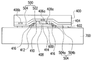
- a carrier such as a lead frame 500 is provided.
- the lead frame 500 has a die pad 502 and a plurality of leads 504 surrounding the die pad 502 .
- Each lead 504 can be further divided into an inner lead section 504 a and an outer lead section 504 b .
- a portion of the leads 504 in the lead frame 500 are ground leads. These ground leads 504 are electrically connected to the heat sink 400 through the first electrical contact 406 b and the die pad 502 on the lead frame 500 is electrically connected to the heat sink 400 through the first electrical contact 406 a.
- the heat sink 400 Since the heat sink 400 has a cavity 402 , a space 506 for accommodating a chip is produced on the lead frame, 500 in a location corresponding to the cavity 402 .
- the chip cavity 506 has a depth that depends on the type of chip to be enclosed inside the package.
- a semiconductor chip 408 is provided.
- the chip 408 can be an ordinary wire-bonding chip or a flip-chip.
- the chip 408 has an active surface 408 a with a plurality of bonding pads 410 thereon.
- a second electrical contact 412 is formed over each bonding pad 410 .
- the second electrical contact 412 are gold bumps or solder bumps, for example.
- the gold bumps can be, for example, gold stud bumps formed by wire bonding or gold stud bumps formed by electroplating.
- a layer of adhesive glue 414 may be applied over the active surface 408 a of the chip 408 . Thereafter, a thermal compression process may be carried out to form electrical connections between the chip 408 and the lead frame 500 .
- the chip 408 is electrically connected to the inner leads 504 a of the lead frame 500 through the second electrical contacts 412 . Meanwhile, the active surface 408 a of the chip 408 also connects electrically with the heat sink 400 via the adhesive glue layer 414 , the die pad 502 and the first electrical contact 406 a.
- an encapsulation process is carried out.
- packaging plastic 416 is injected to fill the entire chip cavity 506 .
- the chip 408 and the lead frame 500 form a solid body.
- a dicing process may be carried out so that each individual package within an array is separated and excess material surrounding a package is removed.
- FIG. 5 is a cross-sectional view after the thermally enhanced package in FIG. 4F joins up with a printed circuit board.
- the package (in FIG. 4F ) mounts on a printed circuit board 700 that serves as its carrier.
- the printed circuit board 700 is electrically connected to the outer leads 504 b of the lead frame 500 so that the chip 408 forms an assembly with the printed circuit board 700 .
- the printed circuit board 700 and the outer leads 504 b of the lead frame 500 are electrically connected through an electrical medium such as third electrical contacts 602 .
- the third electrical contacts 602 may be fabricated with solder paste, for example.
- a heat conductive pad 600 may be inserted in the gap between the printed circuit board 700 and the chip 408 so that heat can be channeled away from the back of the chip 408 via the heat conductive pad 600 to the printed circuit board 700 .
- FIG. 6 is a top view of the lead frame inside the package according to the first embodiment of this invention.
- each lead 504 in the lead frame 500 can be divided into an inner lead section 504 a and an outer lead section 504 b .
- a portion of the junction between the inner leads 504 a a and the die pad 502 may employ a lead break design.
- the lead break design facilitates the detachment of inner leads 504 a from the die pad 502 .
- the lead break design will be removed in a subsequent operation to prevent the inner leads 504 a and the die pad 502 from short-circuiting.
- FIGS. 7A to 7F are schematic cross-sectional views showing the fabrication steps for producing a thermally enhanced package according to a second embodiment of this invention.
- a heat sink 400 having a cavity 402 thereon is provided.
- a layer of adhesive glue 404 is formed over the surface of the cavity 402 .
- the layer of adhesive glue 404 has a plurality of openings 404 a.
- first electrical contacts 406 a , 406 b are formed inside the openings 404 a of the adhesive glue layer 404 .
- the first electrical contacts 406 a , 406 b may protrude slightly above the adhesive glue layer 404 to facilitate subsequent electrical connection with other devices or a host board (not shown).
- a carrier such as a tape carrier 800 is provided.
- the tape carrier comprises a tape 802 , a die pad 804 and a plurality of leads 806 surrounding the die pad 804 .
- Each lead 806 may be further divided into an inner lead section 806 a and an outer lead section 806 b .
- a portion of the leads 806 in the tape carrier 800 are ground leads. These ground leads 806 are electrically connected to the heat sink 400 through the first electrical contact 406 b and the die pad 804 on the tape carrier 800 is electrically connected to the heat sink 400 through the first electrical contact 406 a.
- a hollow space 808 for accommodating a chip is produced on the tape carrier 800 in a location corresponding to the cavity 402 .
- the chip cavity 808 has a depth that depends on the type of chip to be enclosed inside the package.
- a semiconductor chip 408 is provided.
- the chip 408 can be an ordinary wire-bonding chip or a flip-chip.
- the chip 408 has an active surface 408 a with a plurality of bonding pads 410 thereon.
- a second electrical contact 412 is formed over each bonding pad 410 .
- the second electrical contact 412 are gold bumps or solder bumps, for example.
- the gold bumps can be, for example, gold stud bumps formed by wire bonding or gold stud bumps formed by electroplating.
- a layer of adhesive glue 414 may be applied over the active surface 408 a of the chip 408 . Thereafter, a thermal compression process may be carried out to form electrical connections between the chip 408 and the tape carrier 800 .
- the chip 408 is electrically connected to the inner leads 806 a of the tape carrier 800 through the second electrical contacts 412 . Meanwhile, the active surface 408 a of the chip 408 also connects electrically with the heat sink 400 via the adhesive glue layer 414 , the die pad 804 and the first electrical contact 406 a.
- an encapsulation process is carried out.
- packaging plastic 416 is injected to fill the entire chip cavity 808 .
- the chip 408 and the tape carrier 800 form a solid body.
- a dicing process may be carried out so that an individual package within an array is separated and excess material surrounding a package is removed.
- FIG. 8 is a cross-sectional view after the thermally enhanced package in FIG. 7F joins up with a printed circuit board.
- the package (in FIG. 4F ) mounts on a printed circuit board 700 that serves as its carrier.
- the printed circuit board 700 is electrically connected to the outer leads 806 b of the tape carrier 800 so that the chip 408 forms an assembly with the printed circuit board 700 .
- the printed circuit board 700 and the outer leads 806 b of the tape carrier 800 are electrically connected through electrical medium such as third electrical contacts 602 .
- the third electrical contacts 602 may be formed with solder paste, for example.
- a heat conductive pad 600 may be inserted in the gap between the printed circuit board 700 and the chip 408 so that heat can be channeled away from the back side of the chip 408 via the heat conductive pad 600 to the printed circuit board 700 .
- FIGS. 9A to 9C are top views of the tape carrier used in a second embodiment of this invention.
- each lead 806 can be divided into an inner lead section 806 a and an outer lead section 806 b .
- a portion of the junction between the inner leads 806 a and the die pad 804 may employ a lead break design.
- the lead break design facilitates the detachment of inner leads 806 a from the die pad 804 .
- the lead break design will be removed in a subsequent operation to prevent the inner leads 806 a and the die pad 804 from short-circuiting.
- the position of the opening on the tape carrier 800 corresponds to the die pad 804 so that the die pad 804 is directly grounded.
- the die pad 804 and the inner leads 806 a are both supported by the underlying tape 802 .
- the tape 802 underneath the die pad 804 has a plurality of open holes 810 . Through these open holes 810 , the die pad 804 is also grounded.
- the end of each outer lead 806 b includes a connecting pad 812 .
- thermally enhanced package and associated method of fabrication have at least the following advantages:
Abstract
A high performance thermally enhanced package and method of fabricating the same is provided. A chip (a wire bond chip or a flip chip) and a carrier (lead frame or tape carrier) are bonded together using flip-chip technology and thermal compression. The chip and the carrier are encapsulated using a molding compound. The package has a smaller overall size and the capacity to withstand electromagnetic interference.
Description
This application claims the priority benefit of Taiwan application serial no. 91119089, filed Aug. 23, 2002.
1. Field of Invention
The present invention relates to a high performance thermally enhanced package. More particularly, the present invention relates to a high performance thermally enhanced package with a cavity type heat sink therein and a method of fabricating the same.
2. Description of Related Art
In this information conscious society, multi-media applications are developed at a tremendous pace. To complement this trend, integrated circuit packages inside electronic devices must match a set of corresponding demands for digital input, networking, local area connection and personalized usage. In other words, each electronic device must be highly integrated so that more powerful programs can be executed at a higher speed and yet each package has to occupy less space and cost less. Due to the miniaturization and densification of integrated circuit packages, most packages have an edge length only 1.2 times the encapsulated chip or a package area 1.25 times the chip area. Hence, each package is able to provide powerful functions within a very small area. Furthermore, each chip package can be easily mounted on a printed circuit board using standard surface mount technology (SMT) and common equipment. Therefore, chip packages are mostly welcomed by the industry. The most common types of chip packages include bump chip carrier (BCC) package, quad flat nonleaded (QFN) package and lead frame type package.
All the aforementioned packages have a so-called wire-bonding chip design. In other words, the chip is electrically connected to the package through bonding wires. Bonding wires not only increase overall thickness of a package, but also increase overall circuit path compared with a conventional flip-chip packaging technique. Moreover, to package a wire-bonding chip into a flip-chip package, a wiring redistribution is required. After the redistribution process, overall circuit length will be increased so that a parasitic inductance problem may crop up.
Accordingly, one object of the present invention is to provide a thermally enhanced package and a method of fabricating the same that can reduce overall thickness of the package and provide a shorter overall circuit length.
To achieve these and other advantages and in accordance with the purpose of the invention, as embodied and broadly described herein, the invention provides a thermally enhanced package. The thermally enhanced package mainly comprises a heat sink, a carrier, a layer of adhesive glue, a plurality of first electrical contacts, a silicon chip, a plurality of second electrical contacts and a plastic package body. The heat sink has a cavity. The carrier mounts over the heat sink. Since the heat sink has a cavity, a chip cavity for accommodating the silicon chip is formed between the carrier and the heat sink. The heat sink and the carrier are bonded together through the adhesive glue. The layer of adhesive glue has a plurality of openings that exposes the first electrical contacts. Through the first electrical contacts, the heat sink and a portion of the area on the carrier (such as ground leads and die pad) are electrically connected. The chip is enclosed inside the chip cavity above the carrier. The chip is electrically connected to the carrier through the second electrical contacts. The plastic package body fills up the chip cavity so that the chip and the cavity type carrier form a solid body.
In the thermally enhanced package of this invention, the first electrical contacts within the adhesive glue are solder balls, for example. The second electrical contacts for connecting the chip and the carrier electrically are gold bumps or solder bumps. The gold bumps are, for example, the gold stud bumps formed by a wire bond machine or the gold stud bumps formed by electroplating.
The carrier inside the thermally enhanced package is a lead frame, for example. The lead frame includes, for example, a die pad and a plurality of leads around the die pad. Each lead can be divided into an inner lead section and an outer lead section. In addition, the die pad and the outer leads are on a different plane (height), thereby providing a space for accommodating a chip.
The heat sink of the thermally enhanced package is electrically connected to the die pad on the lead frame and a portion of the leads (such as the ground lead) through the first electrical contacts within the adhesive glue. Hence, the heat sink is actually connected to the ground.
In the thermally enhanced package, the gap between the die pad of the lead frame and the active surface of the chip may include a layer of adhesive glue, for example.
The carrier inside the thermally enhanced package may be a tape carrier, for example. The tape carrier comprises a tape, a die pad and a plurality of leads surrounding the die pad. The die pad and the leads are laid on the tape. Each lead is divided into an inner lead section and an outer lead section. In addition, the die pad and the outer leads are on a different plane (at different height levels) to produce a space for accommodating a chip.
The heat sink of the thermally enhanced package is electrically connected to the die pad on the tape carrier and a portion of the leads (such as the ground leads) through the first electrical contacts within the adhesive glue. Hence, the heat sink is actually connected to the ground.
The chip inside the thermally enhanced package may connect to the leads through bonding wires or directly through a flip chip design. Furthermore, adhesive glue may be used to fill the gap between the active surface of the chip and the die pad of the tape carrier.
This invention also provides a method of fabricating a thermally enhanced package. First, a heat sink with a cavity thereon is provided. A layer of adhesive glue with a plurality of openings therein is formed over the heat sink. A first electrical contact is formed inside the openings. A carrier is attached to the heat sink through the adhesive glue. The carrier has a cavity that corresponds in position to the cavity on the heat sink so that a space for accommodating a chip is formed. A silicon chip having an active surface is provided. The active surface of the chip has a plurality of bonding pads thereon. A second electrical contact is formed on each bonding pads of the chip. The chip is next positioned inside the chip cavity followed by conducting a thermal compression process so that the chip and the carrier are electrically connected through the second electrical contacts. Finally, plastic material is injected into the chip cavity in a molding process.
The carrier inside the thermally enhanced package can be a lead frame or a tape carrier and the chip can be a wire-bonding chip or a flip-chip, for example. The second electrical contacts can be any type of metallic bumps such as gold bumps or solder bumps. The gold bumps can be gold stud bumps formed by a wire bond machine or gold stud bumps formed by electroplating.
Before positioning the chip inside the chip cavity in the aforementioned packaging process, adhesive glue may be applied to the active surface of the chip so that the active surface of the chip may connect electrically with the heat sink through the adhesive glue and the carrier. In addition, a dicing process may be conducted to produce individual units after plastic is injected to fill all the chip cavities in an array.
It is to be understood that both the foregoing general description and the following detailed description are exemplary, and are intended to provide further explanation of the invention as claimed.
The accompanying drawings are included to provide a further understanding of the invention, and are incorporated in and constitute a part of this specification. The drawings illustrate embodiments of the invention and, together with the description, serve to explain the principles of the invention. In the drawings,
Reference will now be made in detail to the present preferred embodiments of the invention, examples of which are illustrated in the accompanying drawings. Wherever possible, the same reference numbers are used in the drawings and the description to refer to the same or like parts.
As shown in FIG. 4B , first electrical contacts 406 a, 406 b are formed inside the openings 404 a of the adhesive glue layer 404. The first electrical contacts 406 a, 406 b may protrude slightly above the adhesive glue layer 404 to facilitate subsequent electrical connection with other devices or a host hoard (not shown).
As shown in FIG. 4C , a carrier such as a lead frame 500 is provided. The lead frame 500 has a die pad 502 and a plurality of leads 504 surrounding the die pad 502. Each lead 504 can be further divided into an inner lead section 504 a and an outer lead section 504 b. A portion of the leads 504 in the lead frame 500 are ground leads. These ground leads 504 are electrically connected to the heat sink 400 through the first electrical contact 406 b and the die pad 502 on the lead frame 500 is electrically connected to the heat sink 400 through the first electrical contact 406 a.
Since the heat sink 400 has a cavity 402, a space 506 for accommodating a chip is produced on the lead frame, 500 in a location corresponding to the cavity 402. The chip cavity 506 has a depth that depends on the type of chip to be enclosed inside the package.
As shown in FIG. 4D , a semiconductor chip 408 is provided. The chip 408 can be an ordinary wire-bonding chip or a flip-chip. The chip 408 has an active surface 408 a with a plurality of bonding pads 410 thereon. A second electrical contact 412 is formed over each bonding pad 410. The second electrical contact 412 are gold bumps or solder bumps, for example. The gold bumps can be, for example, gold stud bumps formed by wire bonding or gold stud bumps formed by electroplating. In addition, a layer of adhesive glue 414 may be applied over the active surface 408 a of the chip 408. Thereafter, a thermal compression process may be carried out to form electrical connections between the chip 408 and the lead frame 500. During thermal compression, the chip 408 is electrically connected to the inner leads 504 a of the lead frame 500 through the second electrical contacts 412. Meanwhile, the active surface 408 a of the chip 408 also connects electrically with the heat sink 400 via the adhesive glue layer 414, the die pad 502 and the first electrical contact 406 a.
As shown in FIG. 4E , an encapsulation process is carried out. In the molding process, packaging plastic 416 is injected to fill the entire chip cavity 506. Through the packaging plastic, the chip 408 and the lead frame 500 form a solid body.
As shown in FIG. 4F , a dicing process may be carried out so that each individual package within an array is separated and excess material surrounding a package is removed.
In this embodiment, the printed circuit board 700 and the outer leads 504 b of the lead frame 500 are electrically connected through an electrical medium such as third electrical contacts 602. The third electrical contacts 602 may be fabricated with solder paste, for example. In addition, a heat conductive pad 600 may be inserted in the gap between the printed circuit board 700 and the chip 408 so that heat can be channeled away from the back of the chip 408 via the heat conductive pad 600 to the printed circuit board 700.
As shown in FIG. 7B , first electrical contacts 406 a, 406 b are formed inside the openings 404 a of the adhesive glue layer 404. The first electrical contacts 406 a, 406 b may protrude slightly above the adhesive glue layer 404 to facilitate subsequent electrical connection with other devices or a host board (not shown).
As shown in FIG. 7C , a carrier such as a tape carrier 800 is provided. The tape carrier comprises a tape 802, a die pad 804 and a plurality of leads 806 surrounding the die pad 804. Each lead 806 may be further divided into an inner lead section 806 a and an outer lead section 806 b. A portion of the leads 806 in the tape carrier 800 are ground leads. These ground leads 806 are electrically connected to the heat sink 400 through the first electrical contact 406 b and the die pad 804 on the tape carrier 800 is electrically connected to the heat sink 400 through the first electrical contact 406 a.
Since the heat sink 400 has a cavity 402, a hollow space 808 for accommodating a chip is produced on the tape carrier 800 in a location corresponding to the cavity 402. The chip cavity 808 has a depth that depends on the type of chip to be enclosed inside the package.
As shown in FIG. 7D , a semiconductor chip 408 is provided. The chip 408 can be an ordinary wire-bonding chip or a flip-chip. The chip 408 has an active surface 408 a with a plurality of bonding pads 410 thereon. A second electrical contact 412 is formed over each bonding pad 410. The second electrical contact 412 are gold bumps or solder bumps, for example. The gold bumps can be, for example, gold stud bumps formed by wire bonding or gold stud bumps formed by electroplating. In addition, a layer of adhesive glue 414 may be applied over the active surface 408 a of the chip 408. Thereafter, a thermal compression process may be carried out to form electrical connections between the chip 408 and the tape carrier 800. During thermal compression, the chip 408 is electrically connected to the inner leads 806 a of the tape carrier 800 through the second electrical contacts 412. Meanwhile, the active surface 408 a of the chip 408 also connects electrically with the heat sink 400 via the adhesive glue layer 414, the die pad 804 and the first electrical contact 406 a.
As shown in FIG. 7E , an encapsulation process is carried out. In the process, packaging plastic 416 is injected to fill the entire chip cavity 808. Through the packaging plastic, the chip 408 and the tape carrier 800 form a solid body.
As shown in FIG. 7F , a dicing process may be carried out so that an individual package within an array is separated and excess material surrounding a package is removed.
In this embodiment, the printed circuit board 700 and the outer leads 806 b of the tape carrier 800 are electrically connected through electrical medium such as third electrical contacts 602. The third electrical contacts 602 may be formed with solder paste, for example. In addition, a heat conductive pad 600 may be inserted in the gap between the printed circuit board 700 and the chip 408 so that heat can be channeled away from the back side of the chip 408 via the heat conductive pad 600 to the printed circuit board 700.
As shown in FIG. 9A , the position of the opening on the tape carrier 800 corresponds to the die pad 804 so that the die pad 804 is directly grounded. In FIGS. 9B and 9C , the die pad 804 and the inner leads 806 a are both supported by the underlying tape 802. Furthermore, the tape 802 underneath the die pad 804 has a plurality of open holes 810. Through these open holes 810, the die pad 804 is also grounded. Moreover, in FIG. 9C , the end of each outer lead 806 b includes a connecting pad 812.
In summary, the thermally enhanced package and associated method of fabrication have at least the following advantages:
-
- 1. Using either a lead frame or a tape carrier, overall area and thickness of the package can be reduced.
- 2. The heat sink in the package is connected to ground through electrical contacts and hence the heat sink can serve as an electromagnetic interference shield.
- 3. There is no need to use bonding wires to serve as an electrical connection medium. Hence, overall package size can be reduced.
- 4. The package permits not only the use of flip chips, but also the direct electrical connection between a wiring chip and a lead frame. Since there is no need for redistribution, overall circuit length is reduced and hence problems caused by parasitic induction are minimized. In addition, time for developing and cost for producing a new type of chip is shortened.
- 5. When flip-chip technique is combined with thermal compression to fabricate the package, yield and reliability of the package is improved. The shortening of average circuit path provides superior linear operation characteristics.
- 6. Soldering material is not required to join the tape carrier and the chip. Hence, bump pitch can be further reduced to about 45 μm.
- 7. The tape carrier can be designed into a variety of shapes for accommodating different types of chips.
It will be apparent to those skilled in the art that various modifications and variations can be made to the structure of the present invention without departing from the scope or spirit of the invention. In view of the foregoing, it is intended that the present invention cover modifications and variations of this invention provided they fall within the scope of the following claims and their equivalents.
Claims (24)
1. A high performance thermally enhanced package, comprising:
a heat sink having a cavity thereon;
a carrier on the heat sink, wherein the carrier has a cavity in a location corresponding to the cavity in the heat sink for accommodating a chip, wherein the chip is a flip chip;
a layer of adhesive glue between the heat sink and the carrier, wherein the adhesive glue layer has a plurality of openings therein;
a first electrical contact inside each opening such that the carrier and the heat sink is electrically connected;
a chip positioned inside the chip cavity above the heat sink, wherein the chip has an active surface with a plurality of bonding pads thereon; and
a plurality of second electrical contacts between the bonding pads and the carrier such that the chip and the carrier are electrically connected.
2. The package of claim 1 , wherein the carrier is a lead frame comprising:
a die pad; and
a plurality of leads surrounding the die pad, wherein each lead can be divided into an inner lead section and an outer lead section, and the die pad and the outer leads are on a different plane to form the chip cavity for accommodating the chip.
3. The package of claim 2 , wherein the die pad is electrically connected to the heat sink through the first electrical contacts.
4. The package of claim 2 , wherein a portion of the leads is electrically connected to the heat sink through the first electrical contacts.
5. The package of claim 2 , wherein the package further includes another layer of adhesive glue between the die pad and the active surface of the chip.
6. The package of claim 1 , wherein the carrier is a tape carrier comprising:
a tape;
a die pad on the tape; and
a plurality of leads surrounding the die pad, wherein each lead can be divided into an inner lead section and an outer lead section, and the die pad and the outer leads are on different planes to form the cavity for accommodating the chip.
7. The package of claim 6 , wherein the die pad is electrically connected to the heat sink through the first electrical contacts.
8. The package of claim 6 , wherein a portion of the leads is electrically connected to the heat sink through the first electrical contacts.
9. The package of claim 6 , wherein the package may further include another layer of adhesive glue between the die pad and the active surface of the chip.
10. The package of claim 1 , wherein the package may further include a plastic package body filling up the chip cavity so that the chip and the cavity carrier form a solid body.
11. A high performance thermally enhanced package, comprising:
a heat sink having a cavity thereon;
a carrier on the heat sink, wherein the carrier has a cavity in a location corresponding to the cavity in the heat sink for accommodating a chip;
a layer of adhesive glue between the heat sink and the carrier, wherein the adhesive glue layer has a plurality of openings therein;
a first electrical contact inside each opening such tat the carrier and the heat sink is electrically connected;
a chip positioned inside the chip cavity above the heat sink, wherein the chip has an active surface with a plurality of bonding pads thereon; and
a plurality of second electrical contacts between the bonding pads and the carrier such that the chip and the cater are electrically connected, wherein the cater is a lead frame comprising:
a die pad; and
a plurality of leads surrounding the die pad, wherein each lead can be divided into an inner lead section and an outer lead section, and the die pad and the outer leads are on a different plane to form the chip cavity for accommodating the chip.
12. The package of claim 11 , wherein the die pad is electrically connected to the heat sink through the first electrical contacts.
13. The package of claim 11 , wherein a portion of the leads is electrically connected to the heat sink through the first electrical contacts.
14. The package of claim 11 , wherein the package further includes another layer of adhesive glue between the die pad and the active surface of the chip.
15. The package of claim 11 , wherein the chip is a wire bond chip.
16. The package of claim 11 , wherein the chip is a flip chip.
17. The package of claim 11 , wherein the package may further include a plastic package body filling up the chip cavity so that the chip and the cavity carrier form a solid body.
18. A high performance thermally enhanced package, comprising:
a heat sink having a cavity thereon;
a carrier on the heat sink, wherein the carrier has a cavity in a location corresponding to the cavity in the heat sink for accommodating a chip;
a layer of adhesive glue between the heat sink and the carrier, wherein the adhesive glue layer has a plurality of openings therein;
a first electrical contact inside each opening such that the carrier and the heat sink is electrically connected;
a chip positioned inside the chip cavity above the heat sink, wherein the chip has an active surface with a plurality of bonding pads thereon; and
a plurality of second electrical contacts between the bonding pads and the carrier such that the chip and the carrier are electrically connected wherein the carrier is a tape carrier comprising:
a tape;
a die pad on the tape; and
a plurality of leads surrounding the die pad, wherein each lead can be divided into an inner lead section and an outer lead section, and the die pad and the outer leads are on different planes to form the cavity for accommodating the chip.
19. The package of claim 18 , wherein the die pad is electrically connected to the heat sink through the first electrical contacts.
20. The package of claim 18 , wherein a portion of the leads is electrically connected to the heat sink through the first electrical contacts.
21. The package of claim 18 , wherein the package may further include another layer of adhesive glue between the die pad and the active surface of the chip.
22. The package of claim 18 , wherein the chip is a wire bond chip.
23. The package of claim 18 , wherein the chip is a flip chip.
24. The package of claim 18 , wherein the package may further include a plastic package body filling up the chip cavity so that the chip and the cavity carrier form a solid body.
Applications Claiming Priority (2)
| Application Number | Priority Date | Filing Date | Title |
|---|---|---|---|
| TW91119089 | 2002-08-23 | ||
| TW091119089A TW571406B (en) | 2002-08-23 | 2002-08-23 | High performance thermally enhanced package and method of fabricating the same |
Publications (2)
| Publication Number | Publication Date |
|---|---|
| US20040036154A1 US20040036154A1 (en) | 2004-02-26 |
| US7173341B2 true US7173341B2 (en) | 2007-02-06 |
Family
ID=31885481
Family Applications (1)
| Application Number | Title | Priority Date | Filing Date |
|---|---|---|---|
| US10/368,337 Expired - Lifetime US7173341B2 (en) | 2002-08-23 | 2003-02-18 | High performance thermally enhanced package and method of fabricating the same |
Country Status (2)
| Country | Link |
|---|---|
| US (1) | US7173341B2 (en) |
| TW (1) | TW571406B (en) |
Cited By (4)
| Publication number | Priority date | Publication date | Assignee | Title |
|---|---|---|---|---|
| US20090115052A1 (en) * | 2007-05-25 | 2009-05-07 | Astralux, Inc. | Hybrid silicon/non-silicon electronic device with heat spreader |
| US20100096742A1 (en) * | 2004-05-11 | 2010-04-22 | Taiwan Semiconductor Manufacturing Company, Ltd. | Cut-out heat slug for integrated circuit device packaging |
| US20100264533A1 (en) * | 2009-04-16 | 2010-10-21 | Mediatek Inc. | Semiconductor chip package |
| US20110012241A1 (en) * | 2008-03-18 | 2011-01-20 | Mediatek Inc. | Semiconductor Chip Package |
Families Citing this family (9)
| Publication number | Priority date | Publication date | Assignee | Title |
|---|---|---|---|---|
| TW200741902A (en) * | 2006-04-17 | 2007-11-01 | Siliconware Precision Industries Co Ltd | Semiconductor package and, chip carrier thereof and method for fabricating the same |
| TWI353047B (en) * | 2006-12-28 | 2011-11-21 | Siliconware Precision Industries Co Ltd | Heat-dissipating-type semiconductor package |
| US7675131B2 (en) * | 2007-04-05 | 2010-03-09 | Micron Technology, Inc. | Flip-chip image sensor packages and methods of fabricating the same |
| US7993092B2 (en) * | 2007-08-14 | 2011-08-09 | Samsung Electronics Co., Ltd. | Moving carrier for lead frame and method of moving lead frame using the moving carrier |
| US8093714B2 (en) * | 2009-12-10 | 2012-01-10 | Semtech Corporation | Chip assembly with chip-scale packaging |
| US8742597B2 (en) * | 2012-06-29 | 2014-06-03 | Intel Corporation | Package substrates with multiple dice |
| US9490188B2 (en) * | 2014-09-12 | 2016-11-08 | International Business Machines Corporation | Compute intensive module packaging |
| US9496194B2 (en) * | 2014-11-07 | 2016-11-15 | International Business Machines Corporation | Customized module lid |
| DE102018122515B4 (en) * | 2018-09-14 | 2020-03-26 | Infineon Technologies Ag | Method for producing a semiconductor oxide or glass-based connecting body with a wiring structure |
Citations (1)
| Publication number | Priority date | Publication date | Assignee | Title |
|---|---|---|---|---|
| US6469897B2 (en) * | 2001-01-30 | 2002-10-22 | Siliconware Precision Industries Co., Ltd. | Cavity-down tape ball grid array package assembly with grounded heat sink and method of fabricating the same |
-
2002
- 2002-08-23 TW TW091119089A patent/TW571406B/en not_active IP Right Cessation
-
2003
- 2003-02-18 US US10/368,337 patent/US7173341B2/en not_active Expired - Lifetime
Patent Citations (1)
| Publication number | Priority date | Publication date | Assignee | Title |
|---|---|---|---|---|
| US6469897B2 (en) * | 2001-01-30 | 2002-10-22 | Siliconware Precision Industries Co., Ltd. | Cavity-down tape ball grid array package assembly with grounded heat sink and method of fabricating the same |
Cited By (10)
| Publication number | Priority date | Publication date | Assignee | Title |
|---|---|---|---|---|
| US20100096742A1 (en) * | 2004-05-11 | 2010-04-22 | Taiwan Semiconductor Manufacturing Company, Ltd. | Cut-out heat slug for integrated circuit device packaging |
| US8222731B2 (en) * | 2004-05-11 | 2012-07-17 | Taiwan Semiconductor Manufacturing Company, Ltd. | Cut-out heat slug for integrated circuit device packaging |
| US20090115052A1 (en) * | 2007-05-25 | 2009-05-07 | Astralux, Inc. | Hybrid silicon/non-silicon electronic device with heat spreader |
| US20110012241A1 (en) * | 2008-03-18 | 2011-01-20 | Mediatek Inc. | Semiconductor Chip Package |
| US20110012244A1 (en) * | 2008-03-18 | 2011-01-20 | Mediatek Inc. | Semiconductor Chip Package |
| US8106490B2 (en) * | 2008-03-18 | 2012-01-31 | Mediatek Inc. | Semiconductor chip package |
| US8212343B2 (en) | 2008-03-18 | 2012-07-03 | Mediatek Inc. | Semiconductor chip package |
| US20100264533A1 (en) * | 2009-04-16 | 2010-10-21 | Mediatek Inc. | Semiconductor chip package |
| US8018037B2 (en) | 2009-04-16 | 2011-09-13 | Mediatek Inc. | Semiconductor chip package |
| US8288848B2 (en) | 2009-04-16 | 2012-10-16 | Mediatek Inc. | Semiconductor chip package including a lead frame |
Also Published As
| Publication number | Publication date |
|---|---|
| TW571406B (en) | 2004-01-11 |
| US20040036154A1 (en) | 2004-02-26 |
Similar Documents
| Publication | Publication Date | Title |
|---|---|---|
| US6731015B2 (en) | Super low profile package with stacked dies | |
| US6528876B2 (en) | Semiconductor package having heat sink attached to substrate | |
| US6853070B2 (en) | Die-down ball grid array package with die-attached heat spreader and method for making the same | |
| US5508556A (en) | Leaded semiconductor device having accessible power supply pad terminals | |
| US7439099B1 (en) | Thin ball grid array package | |
| US6201302B1 (en) | Semiconductor package having multi-dies | |
| US6414381B1 (en) | Interposer for separating stacked semiconductor chips mounted on a multi-layer printed circuit board | |
| US20020096785A1 (en) | Semiconductor device having stacked multi chip module structure | |
| US20020140085A1 (en) | Semiconductor package including passive elements and method of manufacture | |
| US8420452B2 (en) | Fabrication method of leadframe-based semiconductor package | |
| US6876087B2 (en) | Chip scale package with heat dissipating part | |
| US6753599B2 (en) | Semiconductor package and mounting structure on substrate thereof and stack structure thereof | |
| US6501164B1 (en) | Multi-chip semiconductor package with heat dissipating structure | |
| US7173341B2 (en) | High performance thermally enhanced package and method of fabricating the same | |
| US20080308951A1 (en) | Semiconductor package and fabrication method thereof | |
| US7291924B2 (en) | Flip chip stacked package | |
| US6894904B2 (en) | Tab package | |
| US7015591B2 (en) | Exposed pad module integrating a passive device therein | |
| US6819565B2 (en) | Cavity-down ball grid array semiconductor package with heat spreader | |
| JP3148718B2 (en) | Thermally and electrically enhanced semiconductor package | |
| US20040150099A1 (en) | Cavity down MCM package | |
| US6160311A (en) | Enhanced heat dissipating chip scale package method and devices | |
| KR100726762B1 (en) | Semiconductor lead frame and semiconductor package applying the same | |
| KR100260996B1 (en) | Array type semiconductor package using a lead frame and its manufacturing method | |
| KR100762871B1 (en) | method for fabricating chip scale package |
Legal Events
| Date | Code | Title | Description |
|---|---|---|---|
| AS | Assignment |
Owner name: VIA TECHNOLOGIES, INC., TAIWAN Free format text: ASSIGNMENT OF ASSIGNORS INTEREST;ASSIGNORS:HO, KWUN-YAO;KUNG, MORISS;REEL/FRAME:013793/0564 Effective date: 20021023 |
|
| STCF | Information on status: patent grant |
Free format text: PATENTED CASE |
|
| FPAY | Fee payment |
Year of fee payment: 4 |
|
| FPAY | Fee payment |
Year of fee payment: 8 |
|
| MAFP | Maintenance fee payment |
Free format text: PAYMENT OF MAINTENANCE FEE, 12TH YEAR, LARGE ENTITY (ORIGINAL EVENT CODE: M1553) Year of fee payment: 12 |