US7166325B2 - Carbon nanotube devices - Google Patents
Carbon nanotube devices Download PDFInfo
- Publication number
- US7166325B2 US7166325B2 US10/299,610 US29961002A US7166325B2 US 7166325 B2 US7166325 B2 US 7166325B2 US 29961002 A US29961002 A US 29961002A US 7166325 B2 US7166325 B2 US 7166325B2
- Authority
- US
- United States
- Prior art keywords
- nanotube
- catalyst
- catalyst islands
- islands
- nanotubes
- Prior art date
- Legal status (The legal status is an assumption and is not a legal conclusion. Google has not performed a legal analysis and makes no representation as to the accuracy of the status listed.)
- Expired - Fee Related, expires
Links
- OKTJSMMVPCPJKN-UHFFFAOYSA-N Carbon Chemical compound [C] OKTJSMMVPCPJKN-UHFFFAOYSA-N 0.000 title claims description 59
- 239000002041 carbon nanotube Substances 0.000 title claims description 42
- 229910021393 carbon nanotube Inorganic materials 0.000 title claims description 41
- 239000002071 nanotube Substances 0.000 claims abstract description 176
- 239000003054 catalyst Substances 0.000 claims abstract description 78
- 239000000463 material Substances 0.000 claims abstract description 29
- 239000002923 metal particle Substances 0.000 claims abstract description 4
- 238000000034 method Methods 0.000 claims description 30
- 239000000758 substrate Substances 0.000 claims description 28
- 229910052751 metal Inorganic materials 0.000 claims description 25
- 239000002184 metal Substances 0.000 claims description 25
- 239000002109 single walled nanotube Substances 0.000 claims description 20
- 125000003396 thiol group Chemical class [H]S* 0.000 claims description 15
- PXHVJJICTQNCMI-UHFFFAOYSA-N Nickel Chemical compound [Ni] PXHVJJICTQNCMI-UHFFFAOYSA-N 0.000 claims description 14
- 239000004215 Carbon black (E152) Substances 0.000 claims description 12
- 229930195733 hydrocarbon Natural products 0.000 claims description 12
- 150000002430 hydrocarbons Chemical class 0.000 claims description 12
- 239000003795 chemical substances by application Substances 0.000 claims description 11
- PCHJSUWPFVWCPO-UHFFFAOYSA-N gold Chemical compound [Au] PCHJSUWPFVWCPO-UHFFFAOYSA-N 0.000 claims description 10
- 229910052737 gold Inorganic materials 0.000 claims description 10
- 239000010931 gold Substances 0.000 claims description 10
- VNWKTOKETHGBQD-UHFFFAOYSA-N methane Chemical compound C VNWKTOKETHGBQD-UHFFFAOYSA-N 0.000 claims description 10
- VYPSYNLAJGMNEJ-UHFFFAOYSA-N silicon dioxide Inorganic materials O=[Si]=O VYPSYNLAJGMNEJ-UHFFFAOYSA-N 0.000 claims description 10
- PNEYBMLMFCGWSK-UHFFFAOYSA-N aluminium oxide Inorganic materials [O-2].[O-2].[O-2].[Al+3].[Al+3] PNEYBMLMFCGWSK-UHFFFAOYSA-N 0.000 claims description 9
- 238000000151 deposition Methods 0.000 claims description 9
- 239000011248 coating agent Substances 0.000 claims description 8
- 238000000576 coating method Methods 0.000 claims description 8
- 238000011049 filling Methods 0.000 claims description 8
- 239000002105 nanoparticle Substances 0.000 claims description 8
- 229910052710 silicon Inorganic materials 0.000 claims description 8
- 239000010703 silicon Substances 0.000 claims description 8
- 229910052759 nickel Inorganic materials 0.000 claims description 7
- KDLHZDBZIXYQEI-UHFFFAOYSA-N Palladium Chemical compound [Pd] KDLHZDBZIXYQEI-UHFFFAOYSA-N 0.000 claims description 6
- 229910045601 alloy Inorganic materials 0.000 claims description 6
- 239000000956 alloy Substances 0.000 claims description 6
- 238000004519 manufacturing process Methods 0.000 claims description 6
- JEIPFZHSYJVQDO-UHFFFAOYSA-N iron(III) oxide Inorganic materials O=[Fe]O[Fe]=O JEIPFZHSYJVQDO-UHFFFAOYSA-N 0.000 claims description 5
- 102000004190 Enzymes Human genes 0.000 claims description 4
- 108090000790 Enzymes Proteins 0.000 claims description 4
- XEEYBQQBJWHFJM-UHFFFAOYSA-N Iron Chemical compound [Fe] XEEYBQQBJWHFJM-UHFFFAOYSA-N 0.000 claims description 4
- GWEVSGVZZGPLCZ-UHFFFAOYSA-N Titan oxide Chemical compound O=[Ti]=O GWEVSGVZZGPLCZ-UHFFFAOYSA-N 0.000 claims description 4
- BASFCYQUMIYNBI-UHFFFAOYSA-N platinum Chemical compound [Pt] BASFCYQUMIYNBI-UHFFFAOYSA-N 0.000 claims description 4
- 239000010453 quartz Substances 0.000 claims description 4
- 229910052581 Si3N4 Inorganic materials 0.000 claims description 3
- 229910052763 palladium Inorganic materials 0.000 claims description 3
- 229920000642 polymer Polymers 0.000 claims description 3
- 239000000377 silicon dioxide Substances 0.000 claims description 3
- HQVNEWCFYHHQES-UHFFFAOYSA-N silicon nitride Chemical compound N12[Si]34N5[Si]62N3[Si]51N64 HQVNEWCFYHHQES-UHFFFAOYSA-N 0.000 claims description 3
- ZOKXTWBITQBERF-UHFFFAOYSA-N Molybdenum Chemical compound [Mo] ZOKXTWBITQBERF-UHFFFAOYSA-N 0.000 claims description 2
- KJTLSVCANCCWHF-UHFFFAOYSA-N Ruthenium Chemical compound [Ru] KJTLSVCANCCWHF-UHFFFAOYSA-N 0.000 claims description 2
- RTAQQCXQSZGOHL-UHFFFAOYSA-N Titanium Chemical compound [Ti] RTAQQCXQSZGOHL-UHFFFAOYSA-N 0.000 claims description 2
- HCHKCACWOHOZIP-UHFFFAOYSA-N Zinc Chemical compound [Zn] HCHKCACWOHOZIP-UHFFFAOYSA-N 0.000 claims description 2
- 229910017052 cobalt Inorganic materials 0.000 claims description 2
- 239000010941 cobalt Substances 0.000 claims description 2
- GUTLYIVDDKVIGB-UHFFFAOYSA-N cobalt atom Chemical compound [Co] GUTLYIVDDKVIGB-UHFFFAOYSA-N 0.000 claims description 2
- 229910052742 iron Inorganic materials 0.000 claims description 2
- 229910052750 molybdenum Inorganic materials 0.000 claims description 2
- 239000011733 molybdenum Substances 0.000 claims description 2
- 229910052697 platinum Inorganic materials 0.000 claims description 2
- 229910052703 rhodium Inorganic materials 0.000 claims description 2
- 239000010948 rhodium Substances 0.000 claims description 2
- MHOVAHRLVXNVSD-UHFFFAOYSA-N rhodium atom Chemical compound [Rh] MHOVAHRLVXNVSD-UHFFFAOYSA-N 0.000 claims description 2
- 229910052707 ruthenium Inorganic materials 0.000 claims description 2
- 239000004065 semiconductor Substances 0.000 claims description 2
- 239000010936 titanium Substances 0.000 claims description 2
- 229910052719 titanium Inorganic materials 0.000 claims description 2
- 229910052725 zinc Inorganic materials 0.000 claims description 2
- 239000011701 zinc Substances 0.000 claims description 2
- 238000000059 patterning Methods 0.000 claims 3
- 239000007769 metal material Substances 0.000 claims 1
- 230000004044 response Effects 0.000 abstract description 29
- 239000000126 substance Substances 0.000 abstract description 16
- 239000002245 particle Substances 0.000 abstract description 5
- 239000007789 gas Substances 0.000 description 13
- 239000010410 layer Substances 0.000 description 12
- 238000013459 approach Methods 0.000 description 10
- OKKJLVBELUTLKV-UHFFFAOYSA-N Methanol Chemical compound OC OKKJLVBELUTLKV-UHFFFAOYSA-N 0.000 description 9
- 239000012159 carrier gas Substances 0.000 description 8
- 238000001514 detection method Methods 0.000 description 8
- 108090001008 Avidin Proteins 0.000 description 7
- XUIMIQQOPSSXEZ-UHFFFAOYSA-N Silicon Chemical compound [Si] XUIMIQQOPSSXEZ-UHFFFAOYSA-N 0.000 description 7
- 239000000203 mixture Substances 0.000 description 7
- 230000015572 biosynthetic process Effects 0.000 description 6
- 230000008859 change Effects 0.000 description 6
- 230000035945 sensitivity Effects 0.000 description 6
- 239000013626 chemical specie Substances 0.000 description 5
- 230000004048 modification Effects 0.000 description 5
- 238000012986 modification Methods 0.000 description 5
- 238000003786 synthesis reaction Methods 0.000 description 5
- MSNOMDLPLDYDME-UHFFFAOYSA-N gold nickel Chemical compound [Ni].[Au] MSNOMDLPLDYDME-UHFFFAOYSA-N 0.000 description 4
- ZNKMCMOJCDFGFT-UHFFFAOYSA-N gold titanium Chemical compound [Ti].[Au] ZNKMCMOJCDFGFT-UHFFFAOYSA-N 0.000 description 4
- 239000002048 multi walled nanotube Substances 0.000 description 4
- 229920003229 poly(methyl methacrylate) Polymers 0.000 description 4
- 239000004926 polymethyl methacrylate Substances 0.000 description 4
- 229910001258 titanium gold Inorganic materials 0.000 description 4
- 229910052799 carbon Inorganic materials 0.000 description 3
- 230000008878 coupling Effects 0.000 description 3
- 238000010168 coupling process Methods 0.000 description 3
- 238000005859 coupling reaction Methods 0.000 description 3
- 108090000623 proteins and genes Proteins 0.000 description 3
- 229910016874 Fe(NO3) Inorganic materials 0.000 description 2
- WQZGKKKJIJFFOK-GASJEMHNSA-N Glucose Natural products OC[C@H]1OC(O)[C@H](O)[C@@H](O)[C@@H]1O WQZGKKKJIJFFOK-GASJEMHNSA-N 0.000 description 2
- 238000004630 atomic force microscopy Methods 0.000 description 2
- 230000008901 benefit Effects 0.000 description 2
- 238000002485 combustion reaction Methods 0.000 description 2
- 238000011161 development Methods 0.000 description 2
- FAQSSRBQWPBYQC-VGKOASNMSA-N dioxomolybdenum;(z)-4-hydroxypent-3-en-2-one Chemical compound O=[Mo]=O.C\C(O)=C\C(C)=O.C\C(O)=C\C(C)=O FAQSSRBQWPBYQC-VGKOASNMSA-N 0.000 description 2
- 238000000609 electron-beam lithography Methods 0.000 description 2
- 230000008020 evaporation Effects 0.000 description 2
- 238000001704 evaporation Methods 0.000 description 2
- 239000008103 glucose Substances 0.000 description 2
- 230000008569 process Effects 0.000 description 2
- 102000004169 proteins and genes Human genes 0.000 description 2
- 238000011084 recovery Methods 0.000 description 2
- 239000002904 solvent Substances 0.000 description 2
- 238000001179 sorption measurement Methods 0.000 description 2
- 238000012546 transfer Methods 0.000 description 2
- ZOXJGFHDIHLPTG-UHFFFAOYSA-N Boron Chemical compound [B] ZOXJGFHDIHLPTG-UHFFFAOYSA-N 0.000 description 1
- 230000004075 alteration Effects 0.000 description 1
- 238000003491 array Methods 0.000 description 1
- 229910052796 boron Inorganic materials 0.000 description 1
- 125000004432 carbon atom Chemical group C* 0.000 description 1
- 238000006555 catalytic reaction Methods 0.000 description 1
- 238000003759 clinical diagnosis Methods 0.000 description 1
- 239000002131 composite material Substances 0.000 description 1
- 239000004020 conductor Substances 0.000 description 1
- 238000007876 drug discovery Methods 0.000 description 1
- 230000007613 environmental effect Effects 0.000 description 1
- 238000003912 environmental pollution Methods 0.000 description 1
- 238000003920 environmental process Methods 0.000 description 1
- 230000001747 exhibiting effect Effects 0.000 description 1
- 125000000524 functional group Chemical group 0.000 description 1
- 239000011521 glass Substances 0.000 description 1
- 230000003993 interaction Effects 0.000 description 1
- VCJMYUPGQJHHFU-UHFFFAOYSA-N iron(III) nitrate Inorganic materials [Fe+3].[O-][N+]([O-])=O.[O-][N+]([O-])=O.[O-][N+]([O-])=O VCJMYUPGQJHHFU-UHFFFAOYSA-N 0.000 description 1
- 239000007788 liquid Substances 0.000 description 1
- 238000013507 mapping Methods 0.000 description 1
- 238000000968 medical method and process Methods 0.000 description 1
- 229910021404 metallic carbon Inorganic materials 0.000 description 1
- 150000002739 metals Chemical class 0.000 description 1
- VPKDCDLSJZCGKE-UHFFFAOYSA-N methanediimine Chemical compound N=C=N VPKDCDLSJZCGKE-UHFFFAOYSA-N 0.000 description 1
- 238000002156 mixing Methods 0.000 description 1
- 238000012544 monitoring process Methods 0.000 description 1
- 230000009257 reactivity Effects 0.000 description 1
- 238000011160 research Methods 0.000 description 1
- -1 silicon and/or boron Chemical compound 0.000 description 1
- 239000002356 single layer Substances 0.000 description 1
- 230000007847 structural defect Effects 0.000 description 1
- 230000002194 synthesizing effect Effects 0.000 description 1
- 235000012431 wafers Nutrition 0.000 description 1
Images

Classifications
-
- B—PERFORMING OPERATIONS; TRANSPORTING
- B82—NANOTECHNOLOGY
- B82B—NANOSTRUCTURES FORMED BY MANIPULATION OF INDIVIDUAL ATOMS, MOLECULES, OR LIMITED COLLECTIONS OF ATOMS OR MOLECULES AS DISCRETE UNITS; MANUFACTURE OR TREATMENT THEREOF
- B82B1/00—Nanostructures formed by manipulation of individual atoms or molecules, or limited collections of atoms or molecules as discrete units
-
- B—PERFORMING OPERATIONS; TRANSPORTING
- B82—NANOTECHNOLOGY
- B82B—NANOSTRUCTURES FORMED BY MANIPULATION OF INDIVIDUAL ATOMS, MOLECULES, OR LIMITED COLLECTIONS OF ATOMS OR MOLECULES AS DISCRETE UNITS; MANUFACTURE OR TREATMENT THEREOF
- B82B3/00—Manufacture or treatment of nanostructures by manipulation of individual atoms or molecules, or limited collections of atoms or molecules as discrete units
-
- B—PERFORMING OPERATIONS; TRANSPORTING
- B82—NANOTECHNOLOGY
- B82Y—SPECIFIC USES OR APPLICATIONS OF NANOSTRUCTURES; MEASUREMENT OR ANALYSIS OF NANOSTRUCTURES; MANUFACTURE OR TREATMENT OF NANOSTRUCTURES
- B82Y10/00—Nanotechnology for information processing, storage or transmission, e.g. quantum computing or single electron logic
-
- B—PERFORMING OPERATIONS; TRANSPORTING
- B82—NANOTECHNOLOGY
- B82Y—SPECIFIC USES OR APPLICATIONS OF NANOSTRUCTURES; MEASUREMENT OR ANALYSIS OF NANOSTRUCTURES; MANUFACTURE OR TREATMENT OF NANOSTRUCTURES
- B82Y30/00—Nanotechnology for materials or surface science, e.g. nanocomposites
-
- B—PERFORMING OPERATIONS; TRANSPORTING
- B82—NANOTECHNOLOGY
- B82Y—SPECIFIC USES OR APPLICATIONS OF NANOSTRUCTURES; MEASUREMENT OR ANALYSIS OF NANOSTRUCTURES; MANUFACTURE OR TREATMENT OF NANOSTRUCTURES
- B82Y40/00—Manufacture or treatment of nanostructures
-
- C—CHEMISTRY; METALLURGY
- C01—INORGANIC CHEMISTRY
- C01B—NON-METALLIC ELEMENTS; COMPOUNDS THEREOF; METALLOIDS OR COMPOUNDS THEREOF NOT COVERED BY SUBCLASS C01C
- C01B32/00—Carbon; Compounds thereof
- C01B32/15—Nano-sized carbon materials
- C01B32/158—Carbon nanotubes
- C01B32/16—Preparation
- C01B32/162—Preparation characterised by catalysts
-
- G—PHYSICS
- G01—MEASURING; TESTING
- G01N—INVESTIGATING OR ANALYSING MATERIALS BY DETERMINING THEIR CHEMICAL OR PHYSICAL PROPERTIES
- G01N27/00—Investigating or analysing materials by the use of electric, electrochemical, or magnetic means
- G01N27/02—Investigating or analysing materials by the use of electric, electrochemical, or magnetic means by investigating impedance
- G01N27/04—Investigating or analysing materials by the use of electric, electrochemical, or magnetic means by investigating impedance by investigating resistance
- G01N27/12—Investigating or analysing materials by the use of electric, electrochemical, or magnetic means by investigating impedance by investigating resistance of a solid body in dependence upon absorption of a fluid; of a solid body in dependence upon reaction with a fluid, for detecting components in the fluid
- G01N27/125—Composition of the body, e.g. the composition of its sensitive layer
- G01N27/127—Composition of the body, e.g. the composition of its sensitive layer comprising nanoparticles
-
- G—PHYSICS
- G01—MEASURING; TESTING
- G01Q—SCANNING-PROBE TECHNIQUES OR APPARATUS; APPLICATIONS OF SCANNING-PROBE TECHNIQUES, e.g. SCANNING PROBE MICROSCOPY [SPM]
- G01Q70/00—General aspects of SPM probes, their manufacture or their related instrumentation, insofar as they are not specially adapted to a single SPM technique covered by group G01Q60/00
- G01Q70/08—Probe characteristics
- G01Q70/10—Shape or taper
- G01Q70/12—Nanotube tips
-
- G—PHYSICS
- G11—INFORMATION STORAGE
- G11C—STATIC STORES
- G11C13/00—Digital stores characterised by the use of storage elements not covered by groups G11C11/00, G11C23/00, or G11C25/00
- G11C13/02—Digital stores characterised by the use of storage elements not covered by groups G11C11/00, G11C23/00, or G11C25/00 using elements whose operation depends upon chemical change
- G11C13/025—Digital stores characterised by the use of storage elements not covered by groups G11C11/00, G11C23/00, or G11C25/00 using elements whose operation depends upon chemical change using fullerenes, e.g. C60, or nanotubes, e.g. carbon or silicon nanotubes
-
- G—PHYSICS
- G11—INFORMATION STORAGE
- G11C—STATIC STORES
- G11C17/00—Read-only memories programmable only once; Semi-permanent stores, e.g. manually-replaceable information cards
- G11C17/14—Read-only memories programmable only once; Semi-permanent stores, e.g. manually-replaceable information cards in which contents are determined by selectively establishing, breaking or modifying connecting links by permanently altering the state of coupling elements, e.g. PROM
- G11C17/16—Read-only memories programmable only once; Semi-permanent stores, e.g. manually-replaceable information cards in which contents are determined by selectively establishing, breaking or modifying connecting links by permanently altering the state of coupling elements, e.g. PROM using electrically-fusible links
- G11C17/165—Memory cells which are electrically programmed to cause a change in resistance, e.g. to permit multiple resistance steps to be programmed rather than conduct to or from non-conduct change of fuses and antifuses
-
- C—CHEMISTRY; METALLURGY
- C01—INORGANIC CHEMISTRY
- C01B—NON-METALLIC ELEMENTS; COMPOUNDS THEREOF; METALLOIDS OR COMPOUNDS THEREOF NOT COVERED BY SUBCLASS C01C
- C01B2202/00—Structure or properties of carbon nanotubes
- C01B2202/02—Single-walled nanotubes
-
- Y—GENERAL TAGGING OF NEW TECHNOLOGICAL DEVELOPMENTS; GENERAL TAGGING OF CROSS-SECTIONAL TECHNOLOGIES SPANNING OVER SEVERAL SECTIONS OF THE IPC; TECHNICAL SUBJECTS COVERED BY FORMER USPC CROSS-REFERENCE ART COLLECTIONS [XRACs] AND DIGESTS
- Y10—TECHNICAL SUBJECTS COVERED BY FORMER USPC
- Y10S—TECHNICAL SUBJECTS COVERED BY FORMER USPC CROSS-REFERENCE ART COLLECTIONS [XRACs] AND DIGESTS
- Y10S427/00—Coating processes
- Y10S427/102—Fullerene type base or coating
-
- Y—GENERAL TAGGING OF NEW TECHNOLOGICAL DEVELOPMENTS; GENERAL TAGGING OF CROSS-SECTIONAL TECHNOLOGIES SPANNING OVER SEVERAL SECTIONS OF THE IPC; TECHNICAL SUBJECTS COVERED BY FORMER USPC CROSS-REFERENCE ART COLLECTIONS [XRACs] AND DIGESTS
- Y10—TECHNICAL SUBJECTS COVERED BY FORMER USPC
- Y10S—TECHNICAL SUBJECTS COVERED BY FORMER USPC CROSS-REFERENCE ART COLLECTIONS [XRACs] AND DIGESTS
- Y10S977/00—Nanotechnology
- Y10S977/70—Nanostructure
- Y10S977/734—Fullerenes, i.e. graphene-based structures, such as nanohorns, nanococoons, nanoscrolls or fullerene-like structures, e.g. WS2 or MoS2 chalcogenide nanotubes, planar C3N4, etc.
- Y10S977/742—Carbon nanotubes, CNTs
- Y10S977/745—Carbon nanotubes, CNTs having a modified surface
- Y10S977/746—Modified with biological, organic, or hydrocarbon material
-
- Y—GENERAL TAGGING OF NEW TECHNOLOGICAL DEVELOPMENTS; GENERAL TAGGING OF CROSS-SECTIONAL TECHNOLOGIES SPANNING OVER SEVERAL SECTIONS OF THE IPC; TECHNICAL SUBJECTS COVERED BY FORMER USPC CROSS-REFERENCE ART COLLECTIONS [XRACs] AND DIGESTS
- Y10—TECHNICAL SUBJECTS COVERED BY FORMER USPC
- Y10S—TECHNICAL SUBJECTS COVERED BY FORMER USPC CROSS-REFERENCE ART COLLECTIONS [XRACs] AND DIGESTS
- Y10S977/00—Nanotechnology
- Y10S977/84—Manufacture, treatment, or detection of nanostructure
- Y10S977/842—Manufacture, treatment, or detection of nanostructure for carbon nanotubes or fullerenes
- Y10S977/843—Gas phase catalytic growth, i.e. chemical vapor deposition
-
- Y—GENERAL TAGGING OF NEW TECHNOLOGICAL DEVELOPMENTS; GENERAL TAGGING OF CROSS-SECTIONAL TECHNOLOGIES SPANNING OVER SEVERAL SECTIONS OF THE IPC; TECHNICAL SUBJECTS COVERED BY FORMER USPC CROSS-REFERENCE ART COLLECTIONS [XRACs] AND DIGESTS
- Y10—TECHNICAL SUBJECTS COVERED BY FORMER USPC
- Y10S—TECHNICAL SUBJECTS COVERED BY FORMER USPC CROSS-REFERENCE ART COLLECTIONS [XRACs] AND DIGESTS
- Y10S977/00—Nanotechnology
- Y10S977/84—Manufacture, treatment, or detection of nanostructure
- Y10S977/849—Manufacture, treatment, or detection of nanostructure with scanning probe
- Y10S977/86—Scanning probe structure
- Y10S977/875—Scanning probe structure with tip detail
- Y10S977/876—Nanotube tip
-
- Y—GENERAL TAGGING OF NEW TECHNOLOGICAL DEVELOPMENTS; GENERAL TAGGING OF CROSS-SECTIONAL TECHNOLOGIES SPANNING OVER SEVERAL SECTIONS OF THE IPC; TECHNICAL SUBJECTS COVERED BY FORMER USPC CROSS-REFERENCE ART COLLECTIONS [XRACs] AND DIGESTS
- Y10—TECHNICAL SUBJECTS COVERED BY FORMER USPC
- Y10S—TECHNICAL SUBJECTS COVERED BY FORMER USPC CROSS-REFERENCE ART COLLECTIONS [XRACs] AND DIGESTS
- Y10S977/00—Nanotechnology
- Y10S977/84—Manufacture, treatment, or detection of nanostructure
- Y10S977/894—Manufacture, treatment, or detection of nanostructure having step or means utilizing biological growth
-
- Y—GENERAL TAGGING OF NEW TECHNOLOGICAL DEVELOPMENTS; GENERAL TAGGING OF CROSS-SECTIONAL TECHNOLOGIES SPANNING OVER SEVERAL SECTIONS OF THE IPC; TECHNICAL SUBJECTS COVERED BY FORMER USPC CROSS-REFERENCE ART COLLECTIONS [XRACs] AND DIGESTS
- Y10—TECHNICAL SUBJECTS COVERED BY FORMER USPC
- Y10S—TECHNICAL SUBJECTS COVERED BY FORMER USPC CROSS-REFERENCE ART COLLECTIONS [XRACs] AND DIGESTS
- Y10S977/00—Nanotechnology
- Y10S977/84—Manufacture, treatment, or detection of nanostructure
- Y10S977/895—Manufacture, treatment, or detection of nanostructure having step or means utilizing chemical property
-
- Y—GENERAL TAGGING OF NEW TECHNOLOGICAL DEVELOPMENTS; GENERAL TAGGING OF CROSS-SECTIONAL TECHNOLOGIES SPANNING OVER SEVERAL SECTIONS OF THE IPC; TECHNICAL SUBJECTS COVERED BY FORMER USPC CROSS-REFERENCE ART COLLECTIONS [XRACs] AND DIGESTS
- Y10—TECHNICAL SUBJECTS COVERED BY FORMER USPC
- Y10S—TECHNICAL SUBJECTS COVERED BY FORMER USPC CROSS-REFERENCE ART COLLECTIONS [XRACs] AND DIGESTS
- Y10S977/00—Nanotechnology
- Y10S977/902—Specified use of nanostructure
- Y10S977/932—Specified use of nanostructure for electronic or optoelectronic application
- Y10S977/953—Detector using nanostructure
- Y10S977/957—Of chemical property or presence
-
- Y—GENERAL TAGGING OF NEW TECHNOLOGICAL DEVELOPMENTS; GENERAL TAGGING OF CROSS-SECTIONAL TECHNOLOGIES SPANNING OVER SEVERAL SECTIONS OF THE IPC; TECHNICAL SUBJECTS COVERED BY FORMER USPC CROSS-REFERENCE ART COLLECTIONS [XRACs] AND DIGESTS
- Y10—TECHNICAL SUBJECTS COVERED BY FORMER USPC
- Y10T—TECHNICAL SUBJECTS COVERED BY FORMER US CLASSIFICATION
- Y10T428/00—Stock material or miscellaneous articles
- Y10T428/29—Coated or structually defined flake, particle, cell, strand, strand portion, rod, filament, macroscopic fiber or mass thereof
- Y10T428/2913—Rod, strand, filament or fiber
- Y10T428/2918—Rod, strand, filament or fiber including free carbon or carbide or therewith [not as steel]
-
- Y—GENERAL TAGGING OF NEW TECHNOLOGICAL DEVELOPMENTS; GENERAL TAGGING OF CROSS-SECTIONAL TECHNOLOGIES SPANNING OVER SEVERAL SECTIONS OF THE IPC; TECHNICAL SUBJECTS COVERED BY FORMER USPC CROSS-REFERENCE ART COLLECTIONS [XRACs] AND DIGESTS
- Y10—TECHNICAL SUBJECTS COVERED BY FORMER USPC
- Y10T—TECHNICAL SUBJECTS COVERED BY FORMER US CLASSIFICATION
- Y10T428/00—Stock material or miscellaneous articles
- Y10T428/29—Coated or structually defined flake, particle, cell, strand, strand portion, rod, filament, macroscopic fiber or mass thereof
- Y10T428/2913—Rod, strand, filament or fiber
- Y10T428/2973—Particular cross section
- Y10T428/2975—Tubular or cellular
Definitions
- the present invention relates generally to carbon nanotube devices and more particularly to chemical and biological sensors and related applications employing carbon nanotubes.
- Carbon nanotubes are unique carbon-based, molecular structures that exhibit interesting and useful electrical properties.
- SWNTs have a cylindrical sheet-like, one-atom-thick shell of hexagonally-arranged carbon atoms, and MWNTs are typically composed of multiple coaxial cylinders of ever-increasing diameter about a common axis.
- SWNTs can be considered to be the structure underlying MWNTs and also carbon nanotube ropes, which are uniquely-arranged arrays of SWNTs.
- carbon nanotubes Due to their unique electrical properties, carbon nanotubes are being studied for development in a variety of applications. These applications include, among others, chemical and bio-type sensing, field-emission sources, selective-molecule grabbing, nano-electronic devices, and a variety of composite materials with enhanced mechanical and electro-mechanical properties. More specifically, for example, in connection with chemical and biological detection, carbon nanotubes are being studied for applications including medical devices, environmental monitoring, medical/clinical diagnosis and biotechnology for gene mapping and drug discovery. For general information regarding carbon nanotubes, and for specific information regarding SWNTs and its applications, reference may be made generally to the above-mentioned patent documents, and also to: “Carbon Nanotubes: Synthesis, Structure, Properties and Applications,” M. S. Dresselhaus, G. Dresselhaus and Ph.
- Sensing chemical and biological species plays an important role in many industrial, agricultural, medical, and environmental processes. Detection of NO 2 gas, for example, provides a crucial measure of environmental pollution due to combustion or automotive emissions. In industrial, medical and living environments, the amount of NH 3 also needs to be closely monitored. Moreover, there is a growing need to detect biological species in a variety of biomedical applications. However, previously-used sensors typically must operate at elevated temperatures to enhance chemical reactivity, and often require long recovery times (if recoverable at all), poor reproducibility, and are applicable to the detection of a very limited range of chemical species.
- the present invention is directed to overcoming the above-mentioned challenges and others related to carbon nanotube devices and their implementations.
- the present invention is exemplified in a number of implementations and applications, some of which are summarized below.
- a nanotube device is manufactured having a nanotube extending between two conductive elements.
- the conductive elements are coupled to one or more of a variety of circuit elements, such as those typically found in sensors and integrated circuit devices.
- the nanotube device is responsive to a variety of electrical, physical and chemical stimuli, and is adaptable for implementation with many applications, such as for sensing and nanoelectronic applications.
- the nanotube device discussed above is manufactured for use in connection with chemical and/or biological sensor applications.
- individually separable nanotubes are grown in a controlled fashion.
- the nanotube device is manipulated and integrated into a functional device such as an electrical, mechanical and/or electrochemical device that can be individually tailored to a wide range of applications.
- the nanotube device is modified to tune its sensitivity to a variety of molecular and/or biological species using one or more materials disposed on the nanotube.
- electrical, mechanical, and electrochemical nanotube devices including those employing carbon nanotubes, can be individually tailored to a wide range of applications.
- these nanotube devices demonstrate significant and robust response, and more significantly, tunable selectivity to chemical or biological species in selected environments.
- a nanotube device is manufactured having two catalyst islands disposed on a substrate. Each catalyst island is adapted for growing nanotubes when exposed to a hydrocarbon gas at elevated temperatures. Using this approach, at least one nanotube is formed between, with its two ends rooted in, the two catalyst islands. Metal electrodes are then placed to fully cover the catalyst islands and the two ends of the bridging nanotube. The metal electrodes are useful, for example, for electrically coupling the nanotube to other circuitry, such as for measuring an electrical response of the nanotube.
- the selectivity of the nanotube to chemical species is physically tuned for exhibiting a selected response.
- the nanotube device is coated and/or decorated with one or more sensing agents, such as metal particles, polymers, and biological species, which impart sensitivity to the nanotube for particular molecular species.
- a gating voltage is applied to a nanotube and/or by selectively coupling sensing agents to the nanotube. The gating voltage effectively shifts the Fermi energy level of the nanotube, giving rise to change in electrical conductivity of the nanotube upon adsorption of foreign chemical species.
- a nanotube device having a layer of catalyst material over a substrate.
- the layer of catalyst material enables the growth of nanotubes when exposed to a hydrocarbon gas at elevated temperatures, yielding a film of interconnected nanotubes disposed on the substrate.
- Two metal electrodes e.g., an alloy of nickel-gold or titanium-gold
- the substrate is made of quartz and the catalyst comprises Fe 2 O 3 and alumina nanoparticles. Nanotubes thus produced are generally single-walled carbon nanotubes that are semiconducting and/or metallic.
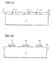
- FIGS. 1A–1C depict a method for synthesizing individually distinct nanotubes on a substrate, according to an example embodiment of the present invention
- FIG. 2 is a nanotube device comprising a single nanotube, according to another example embodiment of the present invention.
- FIGS. 3A–3B show a method for making a nanotube film device, according another example embodiment of the present invention.
- FIGS. 4A–4B show the electrical response of a single nanotube device to NO 2 and NH 3 , respectively, according to other example embodiments of the present invention.
- FIG. 5 shows the electrical response of a gold-decorated single nanotube device exposed to thiol vapor, according to another example embodiment of the present invention
- FIG. 6 displays electrical responses of an as-grown nanotube film device and a PMMA-coated nanotube film device exposed to NO 2 gas, according to another example embodiment of the present invention
- FIGS. 7A–7B show the electrical response of a gold-decorated nanotube film device to thiol vapor and the detection of avidin using a thiol-coated-gold-decorated nanotube film device, according to another example embodiment of the present invention.
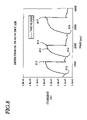
- FIG. 8 displays the detection of H 2 using a palladium-modified nanotube film device, according to another example embodiment of the present invention.
- the present invention is believed to be useful for a variety of different types of devices, and the invention has been found to be particularly suited for carbon nanotube-based sensors and sensing applications, such as for sensing chemical and biological species. While the present invention is not necessarily limited to such applications, various aspects of the invention may be appreciated through a discussion of various examples using this context.
- a nanotube device including a nanotube having electrodes at opposite ends thereof can be manufactured to exhibit selected characteristics useful in a variety of implementations.
- the nanotube is altered physically, chemically or electrically, such as by coating with a metal or other substance or by applying a gating voltage thereto. These alterations tailor the nanotube device to particular applications, such as for making the nanotube respond electrically to a particular molecular species or for making the nanotube respond electrically in a manner similar to semiconducting substrates.
- a carbon nanotube is grown extending between two electrodes and over a semiconductor substrate, such as doped silicon with a layer of oxide formed thereon.
- the electrodes include a catalyst material, such as, Fe 2 O 3 and alumina nanoparticles, and a conductive material disposed thereon, thereby forming conductive catalyst islands (e.g., about 3–5 microns in cross-sectional length).
- the nanotube is a single-walled carbon nanotube.
- the metal electrodes include an alloy such as nickel-gold or titanium-gold.
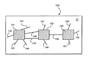
- FIGS. 1A–1C show a carbon nanotube device 100 at various stages of manufacture, with individually distinct nanotubes being formed over a silicon substrate 11 , according to another example embodiment of the present invention.
- a layer of resist 10 is disposed and patterned on a top surface of the substrate 11 .
- the substrate 11 may include, for example, one or more of silicon, alumina, quartz, silica, silicon nitride and/or doped silicon with a layer of native oxide formed thereon.
- the resist 10 is patterned using one or more commonly-available techniques, such as electron-beam lithography, to form a patterned resist structure with openings 112 , 113 and 114 therein that expose the underlying substrate 11 .
- the size of the openings is selected for controlling the size of catalyst islands to be subsequently filled therein, and in one implementation, the openings are about 5 microns in diameter and spaced at a distance of about 10 microns.
- Catalyst material 17 is formed in the openings 112 , 113 and 114 and over the substrate 11 , filling the openings as shown by dashed lines.
- the catalyst material 17 includes about 15 mg of alumina nanoparticles, about 0.05 mmol of Fe(NO 3 )39H 2 O, and about 0.015 mmol of MoO 2 (acac) 2 mixed in about 15 ml of methanol.
- the remaining portion of the resist layer 10 is lifted off after the catalyst material 17 is formed in the openings 112 , 113 and 114 , and in the instance where solvent (i.e., methanol) is used in forming the catalyst material, after the solvent dries.
- An array of isolated catalyst islands including islands 131 , 132 and 133 thus remains over the substrate 11 , with the number, size and orientation of catalyst islands being selected via the formation of the patterned layer of resist 10 .
- the nanotube device 100 is heated to above about 900 degrees Celsius (e.g., in a tube furnace) while exposed to a flow of methane to decompose the Fe(NO 3 ) 3 to a Fe 2 O 3 /nanoparticle (e.g., alumina nanoparticles) mixture, with results shown in FIG. 1C .
- the Fe 2 O 3 /nanoparticle mixture catalyzes the growth of carbon nanotubes when exposed to the methane gas at the elevated temperature and a plurality of carbon nanotubes 141 – 152 are grown as shown.
- the catalyst islands 131 , 132 and 133 optionally include a material such as iron, molybdenum, cobalt, nickel, ruthenium, zinc and oxides thereof, and in one implementation, the catalyst islands are coated with a metal for tailoring die device 100 for use in sensing chemicals.
- the carbon nanotubes grown are predominantly individually distinct, single-walled nanotubes wit few structural defects and are substantially straight, typically extending up to more than 10 microns in length with diameters ranging from 13 nanometers, and in some applications, with diameters of at least about 3 nanometers.
- a number of the carbon nanotubes formed bridge adjacent islands, such as the carbon nanotubes 145 , 146 and 149 . Such a nanotube bridge forms when a tube growing from one catalyst island falls on and interacts with another island during the synthesis process as described above. These bridged nanotubes are useful for a variety of implementations, including those discussed below.
- Nanotube-based chips produced using the techniques discussed in connection with FIGS. 1A–1C can be incorporated into a variety of electronic and mechanical devices.
- nanotubes bridging two catalyst islands are cut mechanically or electrically using an AFM (atomic force microscopy) tip to form a device having a single nanotube bridging two catalyst islands.
- Electron-beam lithography is then employed to deposit metal electrodes onto the two catalyst islands bridged by the nanotube, with the metal electrodes including, for example, an alloy of nickel-gold or titanium-gold.
- the metal electrodes are formed of about 20 nanometers of nickel with 60 nanometers gold on top of the nickel. These electrodes provide electrical connections between the nanotube and macroscopic electronic circuits.
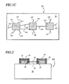
- FIG. 2 shows a nanotube device 200 including a single nanotube 20 disposed between two catalyst islands 21 and 25 on a substrate 22 , according to another example embodiment of the present invention.
- the catalyst islands 21 and 25 and the carbon nanotube 20 may be formed, for example, in a manner similar to that described above in connection with FIGS. 1A–1C .
- the nanotube 20 is formed on the substrate 22 .
- Two metal electrodes 23 and 26 are formed over the catalyst islands 21 and 25 and contacting opposite ends 24 of the carbon nanotube 20 . Electrical contact can then made across the carbon nanotube 20 via the electrodes 23 and 26 for detecting electrical characteristics of the carbon nanotube 20 , such as for detecting a response of the carbon nanotube to exposure to a particular molecular species.
- a gate 29 is optionally disposed below the nanotube 20 and configured and arranged to apply a voltage signal to the nanotube 20 for controlling electrical characteristics thereof.
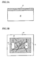
- FIGS. 3A–3B show front and top views, respectively, of a film of nanotubes at stages of synthesis on a substrate, according to another example embodiment of the present invention.
- a layer of catalyst 31 is spin-coated over a substrate 30 , such as a substrate including one or more of: silicon, alumina, quartz, silica and silicon nitride.
- the catalyst 31 is prepared by mixing 15 mg of alumina nanoparticles, 0.05 mmol of Fe(NO 3 )39H 2 O, and 0.015 mmol of MoO 2 (acac) 2 in 15 ml of methanol. After the catalyst layer 31 is formed, the catalyst-covered substrate 30 is heated to above 900° C. in a flow of methane (e.g., as discussed above).
- FIG. 3B shows an interconnected film 32 of single-walled carbon nanotubes on the substrate grown from the catalyzed reaction of the methane.
- Two metal electrodes 33 and 34 are formed over the substrate 30 using, for example, evaporation with a shadow mask (not shown) and with a metal-free gap being between the two electrodes 33 and 34 .
- one or both of the metal electrodes 33 and 34 includes about 20 nanometers of titanium with about 60 nanometers of gold formed thereon.
- one or both of the metal electrodes are made of an alloy, such as nickel-gold or titanium-gold.
- the nanotube film 32 is chemically and/or physically modified, such as by coating the nanotube film 32 with materials such as metals or biological molecules.
- Such modification may, for example, be effected to impart sensitivity of the nanotube film 32 to selected chemical or biological species.
- the nanotube is modified by coupling one or molecules to the nanotube that cause a charge transfer between the nanotube and the molecules, such as via electron withdrawal (e.g., using NO 2 or O 2 ) or electron donation (e.g., using NH 3 ).
- the charge transfer leads to a change in the electrical conductance of the nanotube.
- nanotube devices described above are further physically or chemically modified, in other implementations, so as to be tailored for a particular application.
- a semiconducting or metallic carbon nanotube exhibits a change in electrical conductance when exposed to certain chemical gases. This change may, for example, result from adsorption of the gas particles on the nanotube.
- the sensing agent(s) can be chosen to cause a response of the nanotube to selected molecules (e.g., so that the nanotube exhibits particular characteristics when exposed to the selected molecules).
- the selectivity of the nanotube to chemical species can be also tuned, or changed, by applying a gating voltage to the nanotube, for example, via the gate 29 adjacent to the nanotube 20 in FIG. 2 .
- the gating voltage effectively shifts the Fermi energy level of the nanotube, enabling the nanotube to be more responsive to a particular species.
- a gating voltage in the range of about ⁇ 20 to 20 volts is applied to the nanotube.
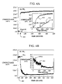
- FIGS. 4A and 4B show electrical responses (conductance versus time) of a device to various amounts of NO 2 and NH 3 gas, respectively, according other example embodiments of the present invention.
- the device includes a semiconducting single-walled carbon nanotube manufactured, for example, in connection with one or more of the example embodiments discussed herein.
- the electrical responses shown may be obtained using the nanotube device 200 of FIG.2 , wherein the nanotube 20 is a single-walled carbon nanotube.
- the single-walled carbon nanotube device is placed in an enclosure, such as a glass flask, equipped with electrical feedthrough (e.g., electrical couplers extending to the carbon nanotube, such as via the electrodes 23 and 26 in FIG. 2 ).
- the electrical feedthrough can be used to make electrical connections between the single-walled carbon nanotube device and electrical detection circuits outside the enclosure.
- a carrier gas e.g., Ar or air
- NO 2 or NH 3 diluted with NO 2 or NH 3
- the single-walled carbon nanotube device exhibits fast and significant response to the introduction of 20 ppm NO 2 and a mixture including 1% NH 3 , respectively, shown at introduction points 410 in FIG.
- FIG. 4A shows a comparison of the resulting change in conductance of the single-walled carbon nanotube device when mixtures of 20 ppm and 2 ppm of NO 2 at curves 412 and 413 , respectively, is introduced.
- curve 422 in FIG. 4B shows the response of the single-walled carbon nanotube device when exposed to a mixture of about 0.1% NH 3 .
- the electrical characteristics of a nanotube exposed to a gas is able to fully recover in a flow of pure carrier gas over a period of several hours.
- a pure carrier gas is flowed over a nanotube device after being used to detect the presence of a gas.
- the pure carrier gas effectively removes interaction of the gas being detected with the nanotube device, and the electrical characteristics of the nanotube device return to that exhibited before introduction of gas.
- the pure carrier gas is flowed such that the single-walled carbon nanotube device returns to a conductance near 0.0, where it was before the introduction of the NO 2 .
- the carrier gas is flowed such that that single-walled carbon nanotube device returns to a conductance of about 1.7e-6, where it was before the introduction of the NH 3 .
- nanotube devices can be implemented as re-usable sensors, with recovery enhanced by the flow of a pure carrier gas.
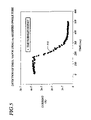
- FIG. 5 shows an electrical response curve 510 of current versus time for a gold-decorated single nanotube to thiol vapor, according to another example embodiment of the present invention.
- the electrical response curve 510 may, for example, be for the nanotube device 200 shown in FIG. 2 with gold applied to the nanotube 20 as a sensing agent.
- gold is deposited on a carbon nanotube by evaporation, which decorates the nanotube (e.g., rather than forming a continuous layer on the nanotube, due to the tendency of gold to not wet carbon).
- the observed response 510 of the nanotube to thiol is affected by the presence of the gold particles.
- a layer of thiol is formed on the gold-decorated nanotube discussed in connection with FIG. 5 above, and the nanotube is subsequently used to link to biological molecules, which is facilitated by the thiol layer.
- the electrical response of the nanotube is detected and used to detect the presence of the biological molecules.
- nanotube devices such as the device 200 in FIG. 2 , can be implemented as a versatile biological sensor.
- FIG. 6 shows electrical responses 610 and 620 (current vs. time) of an as-grown nanotube film device (e.g., including a nanotube mat) and a PMMA (polymethylmethacrylate)-covered nanotube film device to a mixture including about 2 ppm of NO 2 gas, respectively, according to another example embodiment of the present invention.
- the nanotube film device may, for example, include the nanotube film 32 shown in FIG. 3B .
- the PMMA coating is about 100 nanometers thick, and its presence significantly improves the sensitivity and the response time of the nanotube device to NO 2 . More specifically, after the introduction of NO 2 at point 606 , the portion 612 of curve 610 shows a relatively slow response of the device.
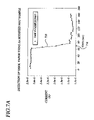
- FIG. 7A shows the electrical response curve 720 (current vs. time) of a gold-decorated nanotube film device to thiol vapor, according to another example embodiment of the present invention.
- gold particles are first evaporated onto a nanotube film, such as the film 32 in FIG. 3B , and a monolayer of thiol with carboxylic functional group is subsequently attached to the nanotube film.
- the presence of thiol modifies the electrical conductance of the nanotube device, with the resulting curve 720 shown with the introduction of thiol vapor at point 710 .
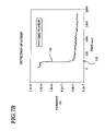
- FIG. 7B shows the detection of avidin (a protein) using a thiol-coated-gold-decorated nanotube film device, such as the device discussed in connection with FIG. 7A , according to another example embodiment of the present invention.
- avidin a protein
- the carboxylic groups of thiol molecules on the thiol-coated-gold-decorated nanotube film device link to avidin molecules via carbodimide chemistry.
- This link to avidin molecules gives rise to a change in electrical conductance of the nanotube film device, shown by curve 730 , with the introduction of the avidin molecules occurring at point 735 .
- the nanotube device is disposed in a liquid environment during introduction of the avidin.
- additional proteins are detected using a similarly-coated nanotube device in a manner not inconsistent with those described herein.
- FIG. 8 shows the detection of H 2 using a Palladium-modified nanotube film device manufactured in connection with another example embodiment of the present invention.
- Palladium particles are deposited onto and decorate a nanotube film, such as film 32 shown in FIG. 3B , with electrodes 33 and 34 being used for detecting an electrical characteristic of the film 32 .
- the Palladium-decorated nanotube responds to H 2 molecules. This response can be used to detect the presence of the H 2 molecules.
- curve 810 shows the response (current vs. time) of the nanotube film with the introduction of a mixture having about 2% H 2 molecules in dry air at curve portions 812 , 814 and 816 .
- the nanotube device recovers when the H 2 is removed (e.g., with dry air or other pure carrier gas being flowed across the device), as shown at curve portions 813 , 815 and 817 .
- an enzyme is attached to a nanotube or a nanotube film, such as the nanotube 20 in FIG. 2 and/or the nanotube film 32 in FIG. 3B . It has been discovered that such an enzyme-coated nanotube or nanotube film exhibits changes in its electrical conductance when exposed to glucose and to biological species. With this approach, nanotube and nanotube film-based sensors, such as those described above, employing enzyme-coated nanotubes can be used for detecting glucose and/or biological species, which is particularly useful in a variety of medical applications.
- various other materials are used to modify the electrical response of nanotubes and/or nanotube films in a manner similar to one or more of the example embodiments and implementations described herein.
- a carbon nanotube can be modified to respond electrically to CO.
- Such an electrical response is useful, for example, for detecting the presence and/or quantity of CO in the exhaust of internal combustion engines.
- metal particles e.g., nickel, rhodium, palladium, TiO 2 , platinum
- polymers, and biological species are used as sensing agents in various implementations to modify the sensitivity of nanotubes to chemical and biological species.
- the nanotubes may be made of materials other than carbon, such as silicon and/or boron, which can also be grown using a synthesis process similar to that described above.
Abstract
Description
Claims (21)
Priority Applications (1)
| Application Number | Priority Date | Filing Date | Title |
|---|---|---|---|
| US10/299,610 US7166325B2 (en) | 1998-08-14 | 2002-11-18 | Carbon nanotube devices |
Applications Claiming Priority (4)
| Application Number | Priority Date | Filing Date | Title |
|---|---|---|---|
| US09/133,948 US6346189B1 (en) | 1998-08-14 | 1998-08-14 | Carbon nanotube structures made using catalyst islands |
| US17120099P | 1999-12-15 | 1999-12-15 | |
| US09/574,393 US6528020B1 (en) | 1998-08-14 | 2000-05-19 | Carbon nanotube devices |
| US10/299,610 US7166325B2 (en) | 1998-08-14 | 2002-11-18 | Carbon nanotube devices |
Related Parent Applications (2)
| Application Number | Title | Priority Date | Filing Date |
|---|---|---|---|
| US09/574,393 Division US6528020B1 (en) | 1998-08-14 | 2000-05-19 | Carbon nanotube devices |
| US09/574,393 Continuation-In-Part US6528020B1 (en) | 1998-08-14 | 2000-05-19 | Carbon nanotube devices |
Publications (2)
| Publication Number | Publication Date |
|---|---|
| US20030068432A1 US20030068432A1 (en) | 2003-04-10 |
| US7166325B2 true US7166325B2 (en) | 2007-01-23 |
Family
ID=22461049
Family Applications (5)
| Application Number | Title | Priority Date | Filing Date |
|---|---|---|---|
| US09/133,948 Expired - Lifetime US6346189B1 (en) | 1998-08-14 | 1998-08-14 | Carbon nanotube structures made using catalyst islands |
| US09/574,393 Expired - Lifetime US6528020B1 (en) | 1998-08-14 | 2000-05-19 | Carbon nanotube devices |
| US10/042,426 Abandoned US20030049444A1 (en) | 1998-08-14 | 2002-01-07 | Carbon nanotube structure having a catalyst island |
| US10/299,610 Expired - Fee Related US7166325B2 (en) | 1998-08-14 | 2002-11-18 | Carbon nanotube devices |
| US10/831,786 Abandoned US20040194705A1 (en) | 1998-08-14 | 2004-04-26 | Apparatus for making carbon nanotube structure with catalyst island |
Family Applications Before (3)
| Application Number | Title | Priority Date | Filing Date |
|---|---|---|---|
| US09/133,948 Expired - Lifetime US6346189B1 (en) | 1998-08-14 | 1998-08-14 | Carbon nanotube structures made using catalyst islands |
| US09/574,393 Expired - Lifetime US6528020B1 (en) | 1998-08-14 | 2000-05-19 | Carbon nanotube devices |
| US10/042,426 Abandoned US20030049444A1 (en) | 1998-08-14 | 2002-01-07 | Carbon nanotube structure having a catalyst island |
Family Applications After (1)
| Application Number | Title | Priority Date | Filing Date |
|---|---|---|---|
| US10/831,786 Abandoned US20040194705A1 (en) | 1998-08-14 | 2004-04-26 | Apparatus for making carbon nanotube structure with catalyst island |
Country Status (2)
| Country | Link |
|---|---|
| US (5) | US6346189B1 (en) |
| WO (1) | WO2000009443A1 (en) |
Cited By (13)
| Publication number | Priority date | Publication date | Assignee | Title |
|---|---|---|---|---|
| US20070032052A1 (en) * | 2000-08-22 | 2007-02-08 | President And Fellows Of Harvard College | Doped elongated semiconductors, growing such semiconductors, devices including such semiconductors, and fabricating such devices |
| US20070048879A1 (en) * | 2004-07-29 | 2007-03-01 | International Business Machines Corporation | Integrated Circuit Chip Utilizing Oriented Carbon Nanotube Conductive Layers |
| US20070164214A1 (en) * | 2006-01-14 | 2007-07-19 | Samsung Electronics Co., Ltd. | Conductive carbon nanotube tip, probe having the conductive carbon nanotube tip, and method of manufacturing the conductive carbon nanotube tip |
| US20090053129A1 (en) * | 2006-04-10 | 2009-02-26 | International Business Machines Corporation | Embedded nanoparticle films and method for their formation in selective areas on a surface |
| US20090236675A1 (en) * | 2008-03-21 | 2009-09-24 | National Tsing Hua University | Self-aligned field-effect transistor structure and manufacturing method thereof |
| US20100108580A1 (en) * | 2008-11-04 | 2010-05-06 | Lukasik Stephen J | Molecular Separators, Concentrators, and Detectors Preparatory to Sensor Operation, and Methods of Minimizing False Positives in Sensor Operations |
| US20100135854A1 (en) * | 2008-12-03 | 2010-06-03 | Electronics And Telecommunications Research Institute | Biosensor having transistor structure and method of fabricating the same |
| US20110012585A1 (en) * | 2007-06-12 | 2011-01-20 | Ford Global Technologies, Llc | Approach for controlling particulate matter in an engine |
| US8431816B2 (en) | 2005-08-24 | 2013-04-30 | The Trustees Of Boston College | Apparatus and methods for solar energy conversion using nanoscale cometal structures |
| US9110055B2 (en) | 2006-11-17 | 2015-08-18 | The Trustees Of Boston College | Nanoscale sensors |
| WO2019075050A1 (en) | 2017-10-10 | 2019-04-18 | Thermo Electron Scientific Instruments Llc | Carbon nanotube-based device for sensing molecular interaction |
| WO2019125844A1 (en) | 2017-12-19 | 2019-06-27 | Thermo Electron Scientific Instruments Llc | Sensor device with carbon nanotube sensor positioned on first and second substrates |
| WO2019133248A1 (en) | 2017-12-28 | 2019-07-04 | Thermo Electron Scientific Instruments Llc | Well plate mixing apparatus |
Families Citing this family (465)
| Publication number | Priority date | Publication date | Assignee | Title |
|---|---|---|---|---|
| JP3740295B2 (en) * | 1997-10-30 | 2006-02-01 | キヤノン株式会社 | Carbon nanotube device, manufacturing method thereof, and electron-emitting device |
| US6346189B1 (en) * | 1998-08-14 | 2002-02-12 | The Board Of Trustees Of The Leland Stanford Junior University | Carbon nanotube structures made using catalyst islands |
| US7416699B2 (en) * | 1998-08-14 | 2008-08-26 | The Board Of Trustees Of The Leland Stanford Junior University | Carbon nanotube devices |
| US7150864B1 (en) * | 1998-09-18 | 2006-12-19 | William Marsh Rice University | Ropes comprised of single-walled and double-walled carbon nanotubes |
| US6692717B1 (en) * | 1999-09-17 | 2004-02-17 | William Marsh Rice University | Catalytic growth of single-wall carbon nanotubes from metal particles |
| US6597090B1 (en) | 1998-09-28 | 2003-07-22 | Xidex Corporation | Method for manufacturing carbon nanotubes as functional elements of MEMS devices |
| US6666075B2 (en) * | 1999-02-05 | 2003-12-23 | Xidex Corporation | System and method of multi-dimensional force sensing for scanning probe microscopy |
| US20060156798A1 (en) * | 2003-12-22 | 2006-07-20 | Vladimir Mancevski | Carbon nanotube excitation system |
| IL129718A0 (en) * | 1999-05-02 | 2000-02-29 | Yeda Res & Dev | Synthesis of nanotubes of transition metal chalcogenides |
| US7816709B2 (en) * | 1999-06-02 | 2010-10-19 | The Board Of Regents Of The University Of Oklahoma | Single-walled carbon nanotube-ceramic composites and methods of use |
| US20030091496A1 (en) * | 2001-07-23 | 2003-05-15 | Resasco Daniel E. | Method and catalyst for producing single walled carbon nanotubes |
| US6333016B1 (en) * | 1999-06-02 | 2001-12-25 | The Board Of Regents Of The University Of Oklahoma | Method of producing carbon nanotubes |
| DE60044972D1 (en) * | 1999-07-02 | 2010-10-28 | Harvard College | NANOSCOPIC WIRE CONTAINING ARRANGEMENT, LOGISC |
| AUPQ304199A0 (en) * | 1999-09-23 | 1999-10-21 | Commonwealth Scientific And Industrial Research Organisation | Patterned carbon nanotubes |
| US7501091B2 (en) * | 1999-12-30 | 2009-03-10 | Smiths Detection Inc. | Sensors with improved properties |
| KR100360470B1 (en) * | 2000-03-15 | 2002-11-09 | 삼성에스디아이 주식회사 | Method for depositing a vertically aligned carbon nanotubes using thermal chemical vapor deposition |
| US6919064B2 (en) * | 2000-06-02 | 2005-07-19 | The Board Of Regents Of The University Of Oklahoma | Process and apparatus for producing single-walled carbon nanotubes |
| US6413487B1 (en) * | 2000-06-02 | 2002-07-02 | The Board Of Regents Of The University Of Oklahoma | Method and apparatus for producing carbon nanotubes |
| DE10134866B4 (en) * | 2000-07-18 | 2005-08-11 | Lg Electronics Inc. | Method of horizontally growing carbon nanotubes and field effect transistor using the process grown carbon nanotubes |
| GB2382718B (en) * | 2000-07-18 | 2004-03-24 | Lg Electronics Inc | Field effect transistor using horizontally grown carbon nanotubes |
| DE10035365B4 (en) * | 2000-07-20 | 2005-02-10 | Infineon Technologies Ag | Method of inferring the existence of light from a dye-bound nanotube |
| US20060175601A1 (en) * | 2000-08-22 | 2006-08-10 | President And Fellows Of Harvard College | Nanoscale wires and related devices |
| US7301199B2 (en) * | 2000-08-22 | 2007-11-27 | President And Fellows Of Harvard College | Nanoscale wires and related devices |
| KR100376768B1 (en) * | 2000-08-23 | 2003-03-19 | 한국과학기술연구원 | Parallel and selective growth and connection method of carbon nanotubes on the substrates for electronic-spintronic device applications |
| WO2002017397A1 (en) * | 2000-08-24 | 2002-02-28 | Infineon Technologies Ag | Electronic element, method for producing an element of this type and a semiconductor element |
| US7258901B1 (en) | 2000-09-08 | 2007-08-21 | Fei Company | Directed growth of nanotubes on a catalyst |
| US6457350B1 (en) * | 2000-09-08 | 2002-10-01 | Fei Company | Carbon nanotube probe tip grown on a small probe |
| US7032437B2 (en) * | 2000-09-08 | 2006-04-25 | Fei Company | Directed growth of nanotubes on a catalyst |
| US6716409B2 (en) | 2000-09-18 | 2004-04-06 | President And Fellows Of The Harvard College | Fabrication of nanotube microscopy tips |
| AU2001294876A1 (en) | 2000-09-29 | 2002-04-08 | President And Fellows Of Harvard College | Direct growth of nanotubes, and their use in nanotweezers |
| US6591658B1 (en) * | 2000-10-25 | 2003-07-15 | Advanced Micro Devices, Inc. | Carbon nanotubes as linewidth standards for SEM & AFM |
| AU2002229046B2 (en) | 2000-12-11 | 2006-05-18 | President And Fellows Of Harvard College | Nanosensors |
| US6515898B2 (en) * | 2001-03-13 | 2003-02-04 | Paul Scherrer Institut (Psi) | Memory element, method for structuring a surface, and storage device |
| US6803840B2 (en) * | 2001-03-30 | 2004-10-12 | California Institute Of Technology | Pattern-aligned carbon nanotube growth and tunable resonator apparatus |
| US6737939B2 (en) * | 2001-03-30 | 2004-05-18 | California Institute Of Technology | Carbon nanotube array RF filter |
| US6689835B2 (en) * | 2001-04-27 | 2004-02-10 | General Electric Company | Conductive plastic compositions and method of manufacture thereof |
| JP2002340506A (en) * | 2001-05-11 | 2002-11-27 | Seiko Instruments Inc | Position detection and electronic clock hand position detector using the same |
| JP3948223B2 (en) * | 2001-05-30 | 2007-07-25 | 株式会社日立製作所 | Gene sequence reader |
| US20030048619A1 (en) * | 2001-06-15 | 2003-03-13 | Kaler Eric W. | Dielectrophoretic assembling of electrically functional microwires |
| JP3557459B2 (en) * | 2001-06-26 | 2004-08-25 | 北海道大学長 | Scanning probe microscope |
| US7186381B2 (en) * | 2001-07-20 | 2007-03-06 | Regents Of The University Of California | Hydrogen gas sensor |
| US6919592B2 (en) | 2001-07-25 | 2005-07-19 | Nantero, Inc. | Electromechanical memory array using nanotube ribbons and method for making same |
| US6835591B2 (en) * | 2001-07-25 | 2004-12-28 | Nantero, Inc. | Methods of nanotube films and articles |
| US6924538B2 (en) * | 2001-07-25 | 2005-08-02 | Nantero, Inc. | Devices having vertically-disposed nanofabric articles and methods of making the same |
| US7566478B2 (en) * | 2001-07-25 | 2009-07-28 | Nantero, Inc. | Methods of making carbon nanotube films, layers, fabrics, ribbons, elements and articles |
| US7563711B1 (en) * | 2001-07-25 | 2009-07-21 | Nantero, Inc. | Method of forming a carbon nanotube-based contact to semiconductor |
| US7259410B2 (en) * | 2001-07-25 | 2007-08-21 | Nantero, Inc. | Devices having horizontally-disposed nanofabric articles and methods of making the same |
| US6706402B2 (en) * | 2001-07-25 | 2004-03-16 | Nantero, Inc. | Nanotube films and articles |
| KR100455284B1 (en) * | 2001-08-14 | 2004-11-12 | 삼성전자주식회사 | High-throughput sensor for detecting biomolecules using carbon nanotubes |
| US6897603B2 (en) * | 2001-08-24 | 2005-05-24 | Si Diamond Technology, Inc. | Catalyst for carbon nanotube growth |
| DE10144704B4 (en) * | 2001-09-11 | 2007-10-04 | Infineon Technologies Ag | Method for connecting a component to a carrier |
| US7318908B1 (en) * | 2001-11-01 | 2008-01-15 | The Board Of Trustees Of The Leland Stanford Junior University | Integrated nanotube sensor |
| US7183228B1 (en) | 2001-11-01 | 2007-02-27 | The Board Of Trustees Of The Leland Stanford Junior University | Carbon nanotube growth |
| US7022541B1 (en) | 2001-11-19 | 2006-04-04 | The Board Of Trustees Of The Leland Stanford Junior University | Patterned growth of single-walled carbon nanotubes from elevated wafer structures |
| US20030124717A1 (en) * | 2001-11-26 | 2003-07-03 | Yuji Awano | Method of manufacturing carbon cylindrical structures and biopolymer detection device |
| US20030143327A1 (en) * | 2001-12-05 | 2003-07-31 | Rudiger Schlaf | Method for producing a carbon nanotube |
| US6835613B2 (en) * | 2001-12-06 | 2004-12-28 | University Of South Florida | Method of producing an integrated circuit with a carbon nanotube |
| FR2833935B1 (en) * | 2001-12-26 | 2004-01-30 | Commissariat Energie Atomique | METHOD FOR MANUFACTURING AT LEAST ONE NANOTUBE BETWEEN TWO ELECTRICALLY CONDUCTIVE ELEMENTS AND DEVICE FOR CARRYING OUT SUCH A METHOD |
| US6784028B2 (en) * | 2001-12-28 | 2004-08-31 | Nantero, Inc. | Methods of making electromechanical three-trace junction devices |
| US20040132070A1 (en) * | 2002-01-16 | 2004-07-08 | Nanomix, Inc. | Nonotube-based electronic detection of biological molecules |
| US8154093B2 (en) | 2002-01-16 | 2012-04-10 | Nanomix, Inc. | Nano-electronic sensors for chemical and biological analytes, including capacitance and bio-membrane devices |
| US20050279987A1 (en) * | 2002-09-05 | 2005-12-22 | Alexander Star | Nanostructure sensor device with polymer recognition layer |
| US20040253741A1 (en) * | 2003-02-06 | 2004-12-16 | Alexander Star | Analyte detection in liquids with carbon nanotube field effect transistor devices |
| US20030134433A1 (en) * | 2002-01-16 | 2003-07-17 | Nanomix, Inc. | Electronic sensing of chemical and biological agents using functionalized nanostructures |
| US8152991B2 (en) | 2005-10-27 | 2012-04-10 | Nanomix, Inc. | Ammonia nanosensors, and environmental control system |
| US20070178477A1 (en) * | 2002-01-16 | 2007-08-02 | Nanomix, Inc. | Nanotube sensor devices for DNA detection |
| US7956525B2 (en) * | 2003-05-16 | 2011-06-07 | Nanomix, Inc. | Flexible nanostructure electronic devices |
| US7955559B2 (en) | 2005-11-15 | 2011-06-07 | Nanomix, Inc. | Nanoelectronic electrochemical test device |
| US20060228723A1 (en) * | 2002-01-16 | 2006-10-12 | Keith Bradley | System and method for electronic sensing of biomolecules |
| US7115305B2 (en) * | 2002-02-01 | 2006-10-03 | California Institute Of Technology | Method of producing regular arrays of nano-scale objects using nano-structured block-copolymeric materials |
| US20030148289A1 (en) * | 2002-02-04 | 2003-08-07 | Intel Corporation | Modified carbon nanotubes as molecular labels with application to DNA sequencing |
| US6958572B2 (en) | 2002-02-06 | 2005-10-25 | Ut-Battelle Llc | Controlled non-normal alignment of catalytically grown nanostructures in a large-scale synthesis process |
| US20070035226A1 (en) * | 2002-02-11 | 2007-02-15 | Rensselaer Polytechnic Institute | Carbon nanotube hybrid structures |
| CA2475790A1 (en) * | 2002-02-11 | 2003-08-21 | Rensselaer Polytechnic Institute | Directed assembly of highly-organized carbon nanotube architectures |
| US7504364B2 (en) * | 2002-03-01 | 2009-03-17 | Receptors Llc | Methods of making arrays and artificial receptors |
| US20070048180A1 (en) * | 2002-09-05 | 2007-03-01 | Gabriel Jean-Christophe P | Nanoelectronic breath analyzer and asthma monitor |
| US7714398B2 (en) * | 2002-09-05 | 2010-05-11 | Nanomix, Inc. | Nanoelectronic measurement system for physiologic gases and improved nanosensor for carbon dioxide |
| US20070048181A1 (en) * | 2002-09-05 | 2007-03-01 | Chang Daniel M | Carbon dioxide nanosensor, and respiratory CO2 monitors |
| US7312095B1 (en) * | 2002-03-15 | 2007-12-25 | Nanomix, Inc. | Modification of selectivity for sensing for nanostructure sensing device arrays |
| AU2003225839A1 (en) * | 2002-03-15 | 2003-09-29 | Nanomix. Inc. | Modification of selectivity for sensing for nanostructure device arrays |
| US7522040B2 (en) * | 2004-04-20 | 2009-04-21 | Nanomix, Inc. | Remotely communicating, battery-powered nanostructure sensor devices |
| US7547931B2 (en) * | 2003-09-05 | 2009-06-16 | Nanomix, Inc. | Nanoelectronic capnometer adaptor including a nanoelectric sensor selectively sensitive to at least one gaseous constituent of exhaled breath |
| US7955483B2 (en) * | 2002-03-18 | 2011-06-07 | Honeywell International Inc. | Carbon nanotube-based glucose sensor |
| US20050161750A1 (en) * | 2002-03-20 | 2005-07-28 | Hongjie Dai | Molybdenum-based electrode with carbon nanotube growth |
| US6831017B1 (en) | 2002-04-05 | 2004-12-14 | Integrated Nanosystems, Inc. | Catalyst patterning for nanowire devices |
| US6871528B2 (en) * | 2002-04-12 | 2005-03-29 | University Of South Florida | Method of producing a branched carbon nanotube for use with an atomic force microscope |
| US7112816B2 (en) * | 2002-04-12 | 2006-09-26 | University Of South Flordia | Carbon nanotube sensor and method of producing the same |
| US20040022943A1 (en) * | 2002-04-12 | 2004-02-05 | Rudiger Schlaf | Carbon nanotube tweezer and a method of producing the same |
| US7335395B2 (en) * | 2002-04-23 | 2008-02-26 | Nantero, Inc. | Methods of using pre-formed nanotubes to make carbon nanotube films, layers, fabrics, ribbons, elements and articles |
| US7381316B1 (en) | 2002-04-30 | 2008-06-03 | Northwestern University | Methods and related systems for carbon nanotube deposition |
| US6689674B2 (en) | 2002-05-07 | 2004-02-10 | Motorola, Inc. | Method for selective chemical vapor deposition of nanotubes |
| US20040067530A1 (en) * | 2002-05-08 | 2004-04-08 | The Regents Of The University Of California | Electronic sensing of biomolecular processes |
| US6774052B2 (en) * | 2002-06-19 | 2004-08-10 | Nantero, Inc. | Method of making nanotube permeable base transistor |
| US7829622B2 (en) * | 2002-06-19 | 2010-11-09 | The Board Of Regents Of The University Of Oklahoma | Methods of making polymer composites containing single-walled carbon nanotubes |
| US7948041B2 (en) | 2005-05-19 | 2011-05-24 | Nanomix, Inc. | Sensor having a thin-film inhibition layer |
| DE10230657B4 (en) * | 2002-07-03 | 2006-04-20 | Leibniz-Institut Für Polymerforschung Dresden E.V. | Method and device for positioning and deforming fusible polymer particles at measuring tips |
| US7013708B1 (en) * | 2002-07-11 | 2006-03-21 | The Board Of Trustees Of The Leland Stanford Junior University | Carbon nanotube sensors |
| WO2004010552A1 (en) | 2002-07-19 | 2004-01-29 | President And Fellows Of Harvard College | Nanoscale coherent optical components |
| JP2005534515A (en) * | 2002-08-01 | 2005-11-17 | ステイト オブ オレゴン アクティング バイ アンド スルー ザ ステイト ボード オブ ハイヤー エデュケーション オン ビハーフ オブ ポートランド ステイト ユニバーシティー | Method for synthesizing nanoscale structure in place |
| JP3804594B2 (en) * | 2002-08-02 | 2006-08-02 | 日本電気株式会社 | Catalyst supporting substrate, carbon nanotube growth method using the same, and transistor using carbon nanotubes |
| US6809384B1 (en) * | 2002-08-09 | 2004-10-26 | Pts Corporation | Method and apparatus for protecting wiring and integrated circuit device |
| US7098056B2 (en) * | 2002-08-09 | 2006-08-29 | Nanoink, Inc. | Apparatus, materials, and methods for fabrication and catalysis |
| US20070114573A1 (en) * | 2002-09-04 | 2007-05-24 | Tzong-Ru Han | Sensor device with heated nanostructure |
| US20060263255A1 (en) * | 2002-09-04 | 2006-11-23 | Tzong-Ru Han | Nanoelectronic sensor system and hydrogen-sensitive functionalization |
| US20050136483A1 (en) * | 2003-09-03 | 2005-06-23 | Receptors Llc | Nanodevices employing combinatorial artificial receptors |
| US20060057625A1 (en) * | 2002-09-16 | 2006-03-16 | Carlson Robert E | Scaffold-based artificial receptors and methods |
| US20050037429A1 (en) * | 2003-03-28 | 2005-02-17 | Receptors Llc | Artificial receptors including reversibly immobilized building blocks and methods |
| WO2005003326A2 (en) * | 2003-03-28 | 2005-01-13 | Receptors Llc. | Artificial receptors including reversibly immobilized building blocks and methods |
| US20050037381A1 (en) * | 2002-09-16 | 2005-02-17 | Receptors Llc | Artificial receptors, building blocks, and methods |
| US7469076B2 (en) * | 2003-09-03 | 2008-12-23 | Receptors Llc | Sensors employing combinatorial artificial receptors |
| US20040137481A1 (en) * | 2002-09-16 | 2004-07-15 | Receptors Llc | Artificial receptor building blocks, components, and kits |
| US7002215B1 (en) * | 2002-09-30 | 2006-02-21 | Pts Corporation | Floating entrance guard for preventing electrical short circuits |
| DE10247679A1 (en) * | 2002-10-12 | 2004-04-22 | Fujitsu Ltd., Kawasaki | Semiconductor body structure, as a biosensor, has two thick layers of one material separated by a thin different intermediate layer forming a nano gap, with organic wire structures as the contacts |
| US7037319B2 (en) * | 2002-10-15 | 2006-05-02 | Scimed Life Systems, Inc. | Nanotube paper-based medical device |
| US20040072994A1 (en) * | 2002-10-15 | 2004-04-15 | Herr Daniel J.C. | Nanostructures including controllably positioned and aligned synthetic nanotubes, and related methods |
| US7253434B2 (en) * | 2002-10-29 | 2007-08-07 | President And Fellows Of Harvard College | Suspended carbon nanotube field effect transistor |
| AU2003304248A1 (en) * | 2002-10-29 | 2005-01-13 | President And Fellows Of Harvard College | Carbon nanotube device fabrication |
| US6998103B1 (en) | 2002-11-15 | 2006-02-14 | The Regents Of The University Of California | Method for producing carbon nanotubes |
| US6949931B2 (en) * | 2002-11-26 | 2005-09-27 | Honeywell International Inc. | Nanotube sensor |
| WO2004051219A2 (en) * | 2002-11-27 | 2004-06-17 | Molecular Nanosystems, Inc. | Nanotube chemical sensor based on work function of electrodes |
| US6780664B1 (en) | 2002-12-20 | 2004-08-24 | Advanced Micro Devices, Inc. | Nanotube tip for atomic force microscope |
| TW580562B (en) * | 2002-12-30 | 2004-03-21 | Ind Tech Res Inst | Apparatus and method for controlling the length of a carbon nanotube |
| CN1745179A (en) * | 2003-01-02 | 2006-03-08 | 拜澳富斯毫微科学有限公司 | Method and apparatus for molecular analysis in small sample volumes |
| US7858185B2 (en) * | 2003-09-08 | 2010-12-28 | Nantero, Inc. | High purity nanotube fabrics and films |
| US8937575B2 (en) | 2009-07-31 | 2015-01-20 | Nantero Inc. | Microstrip antenna elements and arrays comprising a shaped nanotube fabric layer and integrated two terminal nanotube select devices |
| CA2512387A1 (en) * | 2003-01-13 | 2004-08-05 | Nantero, Inc. | Methods of using thin metal layers to make carbon nanotube films, layers, fabrics, ribbons, elements and articles |
| US7560136B2 (en) * | 2003-01-13 | 2009-07-14 | Nantero, Inc. | Methods of using thin metal layers to make carbon nanotube films, layers, fabrics, ribbons, elements and articles |
| US9422651B2 (en) | 2003-01-13 | 2016-08-23 | Nantero Inc. | Methods for arranging nanoscopic elements within networks, fabrics, and films |
| US9574290B2 (en) | 2003-01-13 | 2017-02-21 | Nantero Inc. | Methods for arranging nanotube elements within nanotube fabrics and films |
| US20050112051A1 (en) * | 2003-01-17 | 2005-05-26 | Duke University | Systems and methods for producing single-walled carbon nanotubes (SWNTS) on a substrate |
| US7316061B2 (en) * | 2003-02-03 | 2008-01-08 | Intel Corporation | Packaging of integrated circuits with carbon nano-tube arrays to enhance heat dissipation through a thermal interface |
| US7641863B2 (en) * | 2003-03-06 | 2010-01-05 | Ut-Battelle Llc | Nanoengineered membranes for controlled transport |
| ES2291859T3 (en) * | 2003-03-07 | 2008-03-01 | Seldon Technologies, Llc | PURIFICATION OF FLUIDS WITH NANOMATERIALS. |
| US7419601B2 (en) * | 2003-03-07 | 2008-09-02 | Seldon Technologies, Llc | Nanomesh article and method of using the same for purifying fluids |
| US20040186459A1 (en) * | 2003-03-20 | 2004-09-23 | Michael Shur | Fluid delivery to cells and sensing properties of cells using nanotubes |
| US6918284B2 (en) * | 2003-03-24 | 2005-07-19 | The United States Of America As Represented By The Secretary Of The Navy | Interconnected networks of single-walled carbon nanotubes |
| US7294877B2 (en) | 2003-03-28 | 2007-11-13 | Nantero, Inc. | Nanotube-on-gate FET structures and applications |
| US7022976B1 (en) | 2003-04-02 | 2006-04-04 | Advanced Micro Devices, Inc. | Dynamically adjustable probe tips |
| AU2003250225A1 (en) * | 2003-04-22 | 2004-11-19 | Commissariat A L'energie Atomique | A process for modifying at least one electrical property of a nanotube or a nanowire and a transistor incorporating it. |
| US20040211942A1 (en) * | 2003-04-28 | 2004-10-28 | Clark Darren Cameron | Electrically conductive compositions and method of manufacture thereof |
| WO2004096725A2 (en) * | 2003-04-28 | 2004-11-11 | Leandro Balzano | Single-walled carbon nanotube-ceramic composites and methods of use |
| WO2005019793A2 (en) * | 2003-05-14 | 2005-03-03 | Nantero, Inc. | Sensor platform using a horizontally oriented nanotube element |
| US9234867B2 (en) | 2003-05-16 | 2016-01-12 | Nanomix, Inc. | Electrochemical nanosensors for biomolecule detection |
| US20040232389A1 (en) * | 2003-05-22 | 2004-11-25 | Elkovitch Mark D. | Electrically conductive compositions and method of manufacture thereof |
| US7910064B2 (en) * | 2003-06-03 | 2011-03-22 | Nanosys, Inc. | Nanowire-based sensor configurations |
| US7280394B2 (en) * | 2003-06-09 | 2007-10-09 | Nantero, Inc. | Field effect devices having a drain controlled via a nanotube switching element |
| KR100525764B1 (en) * | 2003-06-13 | 2005-11-04 | 한국과학기술원 | Biosensor using the conductive carbon nanotubes and method thereof |
| US7112472B2 (en) * | 2003-06-25 | 2006-09-26 | Intel Corporation | Methods of fabricating a composite carbon nanotube thermal interface device |
| US7118941B2 (en) * | 2003-06-25 | 2006-10-10 | Intel Corporation | Method of fabricating a composite carbon nanotube thermal interface device |
| US20040262581A1 (en) * | 2003-06-27 | 2004-12-30 | Rodrigues David E. | Electrically conductive compositions and method of manufacture thereof |
| US20050000438A1 (en) * | 2003-07-03 | 2005-01-06 | Lim Brian Y. | Apparatus and method for fabrication of nanostructures using multiple prongs of radiating energy |
| US20050156157A1 (en) * | 2003-07-21 | 2005-07-21 | Parsons Gregory N. | Hierarchical assembly of interconnects for molecular electronics |
| KR20060060682A (en) * | 2003-08-08 | 2006-06-05 | 제너럴 일렉트릭 캄파니 | Electrically conductive compositions comprising carbon nanotubes and method of manufacture thereof |
| US7026432B2 (en) * | 2003-08-12 | 2006-04-11 | General Electric Company | Electrically conductive compositions and method of manufacture thereof |
| US20050036905A1 (en) * | 2003-08-12 | 2005-02-17 | Matsushita Electric Works, Ltd. | Defect controlled nanotube sensor and method of production |
| US7354988B2 (en) * | 2003-08-12 | 2008-04-08 | General Electric Company | Electrically conductive compositions and method of manufacture thereof |
| US7583526B2 (en) | 2003-08-13 | 2009-09-01 | Nantero, Inc. | Random access memory including nanotube switching elements |
| EP1665278A4 (en) | 2003-08-13 | 2007-11-07 | Nantero Inc | Nanotube-based switching elements with multiple controls and circuits made from same |
| JP4669213B2 (en) | 2003-08-29 | 2011-04-13 | 独立行政法人科学技術振興機構 | Field effect transistor, single electron transistor and sensor using the same |
| US7375369B2 (en) * | 2003-09-08 | 2008-05-20 | Nantero, Inc. | Spin-coatable liquid for formation of high purity nanotube films |
| US7416993B2 (en) * | 2003-09-08 | 2008-08-26 | Nantero, Inc. | Patterned nanowire articles on a substrate and methods of making the same |
| WO2005026694A2 (en) * | 2003-09-12 | 2005-03-24 | Nanomix, Inc. | Carbon dioxide nanoelectronic sensor |
| US20050214197A1 (en) * | 2003-09-17 | 2005-09-29 | Molecular Nanosystems, Inc. | Methods for producing and using catalytic substrates for carbon nanotube growth |
| WO2005025734A2 (en) * | 2003-09-17 | 2005-03-24 | Molecular Nanosystems, Inc. | Methods for producing and using catalytic substrates for carbon nanotube growth |
| US7309727B2 (en) * | 2003-09-29 | 2007-12-18 | General Electric Company | Conductive thermoplastic compositions, methods of manufacture and articles derived from such compositions |
| US20050070658A1 (en) * | 2003-09-30 | 2005-03-31 | Soumyadeb Ghosh | Electrically conductive compositions, methods of manufacture thereof and articles derived from such compositions |
| FR2860780B1 (en) * | 2003-10-13 | 2006-05-19 | Centre Nat Rech Scient | METHOD FOR SYNTHESIS OF NANOMETRIC FILAMENT STRUCTURES AND COMPONENTS FOR ELECTRONICS COMPRISING SUCH STRUCTURES |
| US20060024227A1 (en) * | 2003-10-16 | 2006-02-02 | Shigeo Maruyama | Array of single-walled carbon nanotubes and process for preparaton thereof |
| KR20060133974A (en) * | 2003-10-16 | 2006-12-27 | 더 유니버시티 오브 아크론 | Carbon nanotubes on carbon nanofiber substrate |
| US6921684B2 (en) * | 2003-10-17 | 2005-07-26 | Intel Corporation | Method of sorting carbon nanotubes including protecting metallic nanotubes and removing the semiconducting nanotubes |
| US7628974B2 (en) * | 2003-10-22 | 2009-12-08 | International Business Machines Corporation | Control of carbon nanotube diameter using CVD or PECVD growth |
| WO2005066360A1 (en) * | 2003-12-05 | 2005-07-21 | Northwestern University | Micro/nano-fabricated glucose sensors using single-walled carbon nanotubes |
| JP4238716B2 (en) * | 2003-12-15 | 2009-03-18 | 富士ゼロックス株式会社 | Electrode for electrochemical measurement and manufacturing method thereof |
| JP4238715B2 (en) * | 2003-12-15 | 2009-03-18 | 富士ゼロックス株式会社 | Electrochemical measurement electrode |
| CA2549428A1 (en) * | 2003-12-15 | 2005-07-21 | Daniel E. Resasco | Rhenium catalysts and methods for production of single-walled carbon nanotubes |
| US7618300B2 (en) * | 2003-12-24 | 2009-11-17 | Duke University | Method of synthesizing small-diameter carbon nanotubes with electron field emission properties |
| EP1699088A4 (en) * | 2003-12-26 | 2009-08-19 | Fuji Xerox Co Ltd | Rectifying device and electronic circuit employing same, and process for producing rectifying device |
| US7276285B2 (en) * | 2003-12-31 | 2007-10-02 | Honeywell International Inc. | Nanotube fabrication basis |
| US20050151126A1 (en) * | 2003-12-31 | 2005-07-14 | Intel Corporation | Methods of producing carbon nanotubes using peptide or nucleic acid micropatterning |
| EP1748837A4 (en) * | 2004-01-09 | 2009-11-11 | Olga Matarredona | Carbon nanotube pastes and methods of use |
| JP3837568B2 (en) * | 2004-01-23 | 2006-10-25 | 国立大学法人 東京大学 | Carbon nanotube manufacturing method and manufacturing apparatus |
| US7052618B2 (en) * | 2004-01-28 | 2006-05-30 | Agilent Technologies, Inc. | Nanostructures and methods of making the same |
| US7229692B2 (en) * | 2004-02-09 | 2007-06-12 | Ut-Battelle Llc | Nanoconduits and nanoreplicants |
| US7528437B2 (en) * | 2004-02-11 | 2009-05-05 | Nantero, Inc. | EEPROMS using carbon nanotubes for cell storage |
| US7338684B1 (en) * | 2004-02-12 | 2008-03-04 | Performance Polymer Solutions, Inc. | Vapor grown carbon fiber reinforced composite materials and methods of making and using same |
| US20090227107A9 (en) * | 2004-02-13 | 2009-09-10 | President And Fellows Of Havard College | Nanostructures Containing Metal Semiconductor Compounds |
| CN1310024C (en) * | 2004-02-28 | 2007-04-11 | 鸿富锦精密工业(深圳)有限公司 | Probe unit of microscope with atomic force and manufacturing method |
| AU2005219413A1 (en) * | 2004-03-02 | 2005-09-15 | Massachusetts Institute Of Technology | Nanocell drug delivery system |
| US20070053845A1 (en) * | 2004-03-02 | 2007-03-08 | Shiladitya Sengupta | Nanocell drug delivery system |
| KR100583769B1 (en) * | 2004-03-17 | 2006-05-26 | 한국과학기술원 | Carbon Nanotube Cartridge Manufacturing Unit |
| US7341651B2 (en) * | 2004-03-22 | 2008-03-11 | The Regents Of The University Of California | Nanoscale mass conveyors |
| US7276283B2 (en) * | 2004-03-24 | 2007-10-02 | Wisconsin Alumni Research Foundation | Plasma-enhanced functionalization of carbon-containing substrates |
| JP4448356B2 (en) * | 2004-03-26 | 2010-04-07 | 富士通株式会社 | Semiconductor device and manufacturing method thereof |
| US20050221473A1 (en) * | 2004-03-30 | 2005-10-06 | Intel Corporation | Sensor array integrated circuits |
| US20050233263A1 (en) * | 2004-04-20 | 2005-10-20 | Applied Materials, Inc. | Growth of carbon nanotubes at low temperature |
| US20050238810A1 (en) * | 2004-04-26 | 2005-10-27 | Mainstream Engineering Corp. | Nanotube/metal substrate composites and methods for producing such composites |
| JP2007536101A (en) * | 2004-05-05 | 2007-12-13 | カリフォルニア インスティテュート オブ テクノロジー | Nanofiber array capillary lithography |
| US20080023396A1 (en) * | 2004-05-13 | 2008-01-31 | Hokkaido Technology Licensing Office Co., Ltd. | Fine Carbon Dispesion |
| US8075863B2 (en) | 2004-05-26 | 2011-12-13 | Massachusetts Institute Of Technology | Methods and devices for growth and/or assembly of nanostructures |
| US7147534B2 (en) * | 2004-06-04 | 2006-12-12 | Teco Nanotech Co., Ltd. | Patterned carbon nanotube process |
| US7709880B2 (en) * | 2004-06-09 | 2010-05-04 | Nantero, Inc. | Field effect devices having a gate controlled via a nanotube switching element |
| WO2006107312A1 (en) * | 2004-06-15 | 2006-10-12 | President And Fellows Of Harvard College | Nanosensors |
| KR100617470B1 (en) | 2004-06-18 | 2006-08-29 | 전자부품연구원 | AFM cantilever having a carbon nanotube transistor and method for manufacturing the same |
| US7652342B2 (en) | 2004-06-18 | 2010-01-26 | Nantero, Inc. | Nanotube-based transfer devices and related circuits |
| US7161403B2 (en) * | 2004-06-18 | 2007-01-09 | Nantero, Inc. | Storage elements using nanotube switching elements |
| US7164744B2 (en) | 2004-06-18 | 2007-01-16 | Nantero, Inc. | Nanotube-based logic driver circuits |
| US7194912B2 (en) * | 2004-07-13 | 2007-03-27 | United States Of America As Represented By The Administrator Of The National Aeronautics And Space Administration | Carbon nanotube-based sensor and method for continually sensing changes in a structure |
| US7597788B2 (en) * | 2004-07-20 | 2009-10-06 | Applied Nanotech Holdings, Inc. | Oxygen-chemical agent sensor |
| WO2007013872A2 (en) * | 2004-07-22 | 2007-02-01 | The Board Of Trustees Of The University Of Illinois | Sensors employing single-walled carbon nanotubes |
| US7129567B2 (en) * | 2004-08-31 | 2006-10-31 | Micron Technology, Inc. | Substrate, semiconductor die, multichip module, and system including a via structure comprising a plurality of conductive elements |
| US20060042364A1 (en) * | 2004-08-31 | 2006-03-02 | Hongtao Cui | Angled tip for a scanning force microscope |
| JPWO2006025393A1 (en) * | 2004-08-31 | 2008-05-08 | 独立行政法人科学技術振興機構 | Manufacturing method of nano-scale low-dimensional quantum structure and manufacturing method of integrated circuit using the manufacturing method |
| SG135065A1 (en) * | 2006-02-20 | 2007-09-28 | Micron Technology Inc | Conductive vias having two or more elements for providing communication between traces in different substrate planes, semiconductor device assemblies including such vias, and accompanying methods |
| US7504365B2 (en) | 2004-09-03 | 2009-03-17 | Receptors Llc | Combinatorial artificial receptors including tether building blocks |
| WO2006029383A2 (en) * | 2004-09-11 | 2006-03-16 | Receptors Llc | Combinatorial artificial receptors including peptide building blocks |
| WO2006121461A2 (en) * | 2004-09-16 | 2006-11-16 | Nantero, Inc. | Light emitters using nanotubes and methods of making same |
| TWI348169B (en) * | 2004-09-21 | 2011-09-01 | Nantero Inc | Resistive elements using carbon nanotubes |
| US20060084570A1 (en) * | 2004-09-21 | 2006-04-20 | Kopley Thomas E | System and method for growing nanostructures from a periphery of a catalyst layer |
| US7863798B2 (en) * | 2004-10-04 | 2011-01-04 | The Regents Of The University Of California | Nanocrystal powered nanomotor |
| US20070240757A1 (en) * | 2004-10-15 | 2007-10-18 | The Trustees Of Boston College | Solar cells using arrays of optical rectennas |
| US20080090183A1 (en) * | 2004-10-22 | 2008-04-17 | Lingbo Zhu | Aligned Carbon Nanotubes And Method For Construction Thereof |
| JP2006125846A (en) * | 2004-10-26 | 2006-05-18 | Olympus Corp | Cantilever |
| US8021967B2 (en) * | 2004-11-01 | 2011-09-20 | California Institute Of Technology | Nanoscale wicking methods and devices |
| US20100147657A1 (en) * | 2004-11-02 | 2010-06-17 | Nantero, Inc. | Nanotube esd protective devices and corresponding nonvolatile and volatile nanotube switches |
| US7567414B2 (en) | 2004-11-02 | 2009-07-28 | Nantero, Inc. | Nanotube ESD protective devices and corresponding nonvolatile and volatile nanotube switches |
| US7926440B1 (en) | 2004-11-27 | 2011-04-19 | Etamota Corporation | Nanostructure synthesis apparatus and method |
| US7348592B2 (en) | 2004-11-29 | 2008-03-25 | The United States Of America As Represented By The Secretary Of The Navy | Carbon nanotube apparatus and method of carbon nanotube modification |
| CN101124638A (en) * | 2004-12-06 | 2008-02-13 | 哈佛大学 | Nanoscale wire-based data storage |
| WO2006065937A2 (en) * | 2004-12-16 | 2006-06-22 | Nantero, Inc. | Aqueous carbon nanotube applicator liquids and methods for producing applicator liquids thereof |
| US7855021B2 (en) | 2004-12-22 | 2010-12-21 | Brookhaven Science Associates, Llc | Electrocatalysts having platium monolayers on palladium, palladium alloy, and gold alloy core-shell nanoparticles, and uses thereof |
| US7691780B2 (en) * | 2004-12-22 | 2010-04-06 | Brookhaven Science Associates, Llc | Platinum- and platinum alloy-coated palladium and palladium alloy particles and uses thereof |
| US9005331B2 (en) | 2004-12-22 | 2015-04-14 | Brookhaven Science Associates, Llc | Platinum-coated non-noble metal-noble metal core-shell electrocatalysts |
| KR100635546B1 (en) * | 2004-12-24 | 2006-10-17 | 학교법인 포항공과대학교 | Probe of scanning probe microscope having a field effect transistor channel and Fabrication method thereof |
| US7920169B2 (en) * | 2005-01-31 | 2011-04-05 | Invention Science Fund I, Llc | Proximity of shared image devices |
| US7462656B2 (en) * | 2005-02-15 | 2008-12-09 | Sabic Innovative Plastics Ip B.V. | Electrically conductive compositions and method of manufacture thereof |
| CN1830753A (en) * | 2005-03-10 | 2006-09-13 | 清华大学 | Assembling method of carbon nanometer pipe and carbon nanometer pipe device |
| US20090110633A1 (en) * | 2005-03-14 | 2009-04-30 | Shiladitya Sengupta | Nanocells for Diagnosis and Treatment of Diseases and Disorders |
| US7776269B2 (en) * | 2005-03-15 | 2010-08-17 | The United States Of America As Represented By The Secretary Of The Navy | Capacitive based sensing of molecular adsorbates on the surface of single wall nanotubes |
| US20060210467A1 (en) * | 2005-03-17 | 2006-09-21 | Smith Steven M | Producing a stable catalyst for nanotube growth |
| JP4676224B2 (en) * | 2005-03-23 | 2011-04-27 | 東京特殊電線株式会社 | Probe needle and manufacturing method thereof |
| US20060213251A1 (en) * | 2005-03-24 | 2006-09-28 | University Of Florida Research Foundation, Inc. | Carbon nanotube films for hydrogen sensing |
| CN1840465B (en) * | 2005-03-30 | 2010-09-29 | 清华大学 | Method for manufacturing unidimensional nano material device |
| CN100572260C (en) * | 2005-03-31 | 2009-12-23 | 清华大学 | The manufacture method of unidimensional nano material device |
| US20060220006A1 (en) * | 2005-04-01 | 2006-10-05 | Yong Chen | Molecular-doped transistor and sensor |
| US9287356B2 (en) | 2005-05-09 | 2016-03-15 | Nantero Inc. | Nonvolatile nanotube diodes and nonvolatile nanotube blocks and systems using same and methods of making same |
| US8941094B2 (en) | 2010-09-02 | 2015-01-27 | Nantero Inc. | Methods for adjusting the conductivity range of a nanotube fabric layer |
| US9390790B2 (en) | 2005-04-05 | 2016-07-12 | Nantero Inc. | Carbon based nonvolatile cross point memory incorporating carbon based diode select devices and MOSFET select devices for memory and logic applications |
| US8000127B2 (en) | 2009-08-12 | 2011-08-16 | Nantero, Inc. | Method for resetting a resistive change memory element |
| ATE529734T1 (en) * | 2005-04-06 | 2011-11-15 | Harvard College | MOLECULAR CHARACTERIZATION WITH CARBON NANOTUBE CONTROL |
| US20060231946A1 (en) * | 2005-04-14 | 2006-10-19 | Molecular Nanosystems, Inc. | Nanotube surface coatings for improved wettability |
| US7596751B2 (en) * | 2005-04-22 | 2009-09-29 | Hewlett-Packard Development Company, L.P. | Contact sheet based image management |
| US20060251897A1 (en) * | 2005-05-06 | 2006-11-09 | Molecular Nanosystems, Inc. | Growth of carbon nanotubes to join surfaces |
| US9196615B2 (en) * | 2005-05-09 | 2015-11-24 | Nantero Inc. | Nonvolatile nanotube diodes and nonvolatile nanotube blocks and systems using same and methods of making same |
| US8183665B2 (en) * | 2005-11-15 | 2012-05-22 | Nantero Inc. | Nonvolatile nanotube diodes and nonvolatile nanotube blocks and systems using same and methods of making same |
| US7781862B2 (en) * | 2005-05-09 | 2010-08-24 | Nantero, Inc. | Two-terminal nanotube devices and systems and methods of making same |
| US7394687B2 (en) * | 2005-05-09 | 2008-07-01 | Nantero, Inc. | Non-volatile-shadow latch using a nanotube switch |
| US9911743B2 (en) | 2005-05-09 | 2018-03-06 | Nantero, Inc. | Nonvolatile nanotube diodes and nonvolatile nanotube blocks and systems using same and methods of making same |
| US7479654B2 (en) * | 2005-05-09 | 2009-01-20 | Nantero, Inc. | Memory arrays using nanotube articles with reprogrammable resistance |
| US8008745B2 (en) * | 2005-05-09 | 2011-08-30 | Nantero, Inc. | Latch circuits and operation circuits having scalable nonvolatile nanotube switches as electronic fuse replacement elements |
| US8513768B2 (en) * | 2005-05-09 | 2013-08-20 | Nantero Inc. | Nonvolatile nanotube diodes and nonvolatile nanotube blocks and systems using same and methods of making same |
| US8217490B2 (en) * | 2005-05-09 | 2012-07-10 | Nantero Inc. | Nonvolatile nanotube diodes and nonvolatile nanotube blocks and systems using same and methods of making same |
| US7782650B2 (en) * | 2005-05-09 | 2010-08-24 | Nantero, Inc. | Nonvolatile nanotube diodes and nonvolatile nanotube blocks and systems using same and methods of making same |
| TWI324773B (en) * | 2005-05-09 | 2010-05-11 | Nantero Inc | Non-volatile shadow latch using a nanotube switch |
| US7835170B2 (en) * | 2005-05-09 | 2010-11-16 | Nantero, Inc. | Memory elements and cross point switches and arrays of same using nonvolatile nanotube blocks |
| US8102018B2 (en) * | 2005-05-09 | 2012-01-24 | Nantero Inc. | Nonvolatile resistive memories having scalable two-terminal nanotube switches |
| US8013363B2 (en) * | 2005-05-09 | 2011-09-06 | Nantero, Inc. | Nonvolatile nanotube diodes and nonvolatile nanotube blocks and systems using same and methods of making same |
| US8020216B2 (en) | 2005-05-10 | 2011-09-13 | The Regents Of The University Of California | Tapered probe structures and fabrication |
| WO2006119549A1 (en) * | 2005-05-12 | 2006-11-16 | Very Small Particle Company Pty Ltd | Improved catalyst |
| US20060255333A1 (en) * | 2005-05-12 | 2006-11-16 | Kuekes Philip J | Method of forming a controlled distribution of nano-particles on a surface |
| US7598127B2 (en) | 2005-05-12 | 2009-10-06 | Nantero, Inc. | Nanotube fuse structure |
| TWI264271B (en) * | 2005-05-13 | 2006-10-11 | Delta Electronics Inc | Heat sink |
| US7575693B2 (en) * | 2005-05-23 | 2009-08-18 | Nantero, Inc. | Method of aligning nanotubes and wires with an etched feature |
| US20100227382A1 (en) | 2005-05-25 | 2010-09-09 | President And Fellows Of Harvard College | Nanoscale sensors |
| WO2006132659A2 (en) * | 2005-06-06 | 2006-12-14 | President And Fellows Of Harvard College | Nanowire heterostructures |
| US20060278866A1 (en) * | 2005-06-08 | 2006-12-14 | Alexander Star | Nanotube optoelectronic memory devices |
| US7915122B2 (en) * | 2005-06-08 | 2011-03-29 | Nantero, Inc. | Self-aligned cell integration scheme |
| US7278324B2 (en) * | 2005-06-15 | 2007-10-09 | United States Of America As Represented By The Administrator Of The National Aeronautics And Space Administration | Carbon nanotube-based sensor and method for detection of crack growth in a structure |
| WO2007002297A2 (en) | 2005-06-24 | 2007-01-04 | Crafts Douglas E | Temporary planar electrical contact device and method using vertically-compressible nanotube contact structures |
| US20060292716A1 (en) * | 2005-06-27 | 2006-12-28 | Lsi Logic Corporation | Use selective growth metallization to improve electrical connection between carbon nanotubes and electrodes |
| CN101365830B (en) | 2005-06-28 | 2013-06-12 | 俄克拉荷马州大学评议会 | Methods for growing and harvesting carbon nanotubes |
| US7538040B2 (en) * | 2005-06-30 | 2009-05-26 | Nantero, Inc. | Techniques for precision pattern transfer of carbon nanotubes from photo mask to wafers |
| US8000903B1 (en) * | 2005-07-08 | 2011-08-16 | The United States of America as represented by the Administrator of the National Aeronautics and Space Asministration (NASA) | Coated or doped carbon nanotube network sensors as affected by environmental parameters |
| US7801687B1 (en) * | 2005-07-08 | 2010-09-21 | The United States Of America As Represented By The Administrator Of The National Aeronautics And Space Administration (Nasa) | Chemical sensors using coated or doped carbon nanotube networks |
| US7875455B1 (en) | 2005-07-08 | 2011-01-25 | The United States Of America As Represented By The Administrator Of The National Aeronautics And Space Administration (Nasa) | Real time oil reservoir evaluation using nanotechnology |
| US7623972B1 (en) | 2005-07-08 | 2009-11-24 | The United States Of America As Represented By The Administrator Of The National Aeronautics And Space Administration | Detection of presence of chemical precursors |
| WO2007009112A2 (en) * | 2005-07-14 | 2007-01-18 | Colorado School Of Mines | Membrane separation of feed and growth environments in carbon nanostructure growth |
| US7645482B2 (en) * | 2005-08-04 | 2010-01-12 | The Regents Of The University Of California | Method to make and use long single-walled carbon nanotubes as electrical conductors |
| US7718224B2 (en) * | 2005-08-04 | 2010-05-18 | The Regents Of The University Of California | Synthesis of single-walled carbon nanotubes |
| US7170055B1 (en) * | 2005-08-18 | 2007-01-30 | The Board Of Trustees Of The Leland Stanford Junior University | Nanotube arrangements and methods therefor |
| CN100336192C (en) * | 2005-08-18 | 2007-09-05 | 上海交通大学 | Method for bonding nanometer material on metal electrode |
| KR100697323B1 (en) * | 2005-08-19 | 2007-03-20 | 한국기계연구원 | Nano tip and fabrication method of the same |
| US8240190B2 (en) * | 2005-08-23 | 2012-08-14 | Uwm Research Foundation, Inc. | Ambient-temperature gas sensor |
| US8268405B2 (en) | 2005-08-23 | 2012-09-18 | Uwm Research Foundation, Inc. | Controlled decoration of carbon nanotubes with aerosol nanoparticles |
| US7754964B2 (en) * | 2005-08-24 | 2010-07-13 | The Trustees Of Boston College | Apparatus and methods for solar energy conversion using nanocoax structures |
| US7634162B2 (en) * | 2005-08-24 | 2009-12-15 | The Trustees Of Boston College | Apparatus and methods for nanolithography using nanoscale optics |
| US7649665B2 (en) * | 2005-08-24 | 2010-01-19 | The Trustees Of Boston College | Apparatus and methods for optical switching using nanoscale optics |
| US7589880B2 (en) * | 2005-08-24 | 2009-09-15 | The Trustees Of Boston College | Apparatus and methods for manipulating light using nanoscale cometal structures |
| US9084546B2 (en) * | 2005-08-31 | 2015-07-21 | The Regents Of The University Of Michigan | Co-electrodeposited hydrogel-conducting polymer electrodes for biomedical applications |
| US7682453B2 (en) * | 2005-09-01 | 2010-03-23 | Ut-Battelle, Llc | System and method for controlling hydrogen elimination during carbon nanotube synthesis from hydrocarbons |
| WO2008054364A2 (en) | 2005-09-06 | 2008-05-08 | Nantero, Inc. | Carbon nanotubes for the selective transfer of heat from electronics |
| US7850778B2 (en) * | 2005-09-06 | 2010-12-14 | Lemaire Charles A | Apparatus and method for growing fullerene nanotube forests, and forming nanotube films, threads and composite structures therefrom |
| CA2621103C (en) * | 2005-09-06 | 2015-11-03 | Nantero, Inc. | Nanotube fabric-based sensor systems and methods of making same |
| EP1922743A4 (en) * | 2005-09-06 | 2008-10-29 | Nantero Inc | Method and system of using nanotube fabrics as joule heating elements for memories and other applications |
| US7744793B2 (en) | 2005-09-06 | 2010-06-29 | Lemaire Alexander B | Apparatus and method for growing fullerene nanotube forests, and forming nanotube films, threads and composite structures therefrom |
| US7371677B2 (en) * | 2005-09-30 | 2008-05-13 | Freescale Semiconductor, Inc. | Laterally grown nanotubes and method of formation |
| WO2008048313A2 (en) * | 2005-12-19 | 2008-04-24 | Advanced Technology Materials, Inc. | Production of carbon nanotubes |
| US7544523B2 (en) * | 2005-12-23 | 2009-06-09 | Fei Company | Method of fabricating nanodevices |
| US7417119B2 (en) * | 2006-01-17 | 2008-08-26 | Sri International | Nanoscale array biomolecular bond enhancer device |
| US8907384B2 (en) | 2006-01-26 | 2014-12-09 | Nanoselect, Inc. | CNT-based sensors: devices, processes and uses thereof |
| US20090278556A1 (en) * | 2006-01-26 | 2009-11-12 | Nanoselect, Inc. | Carbon Nanostructure Electrode Based Sensors: Devices, Processes and Uses Thereof |
| US20070176255A1 (en) * | 2006-01-31 | 2007-08-02 | Franz Kreupl | Integrated circuit arrangement |
| US20070207182A1 (en) * | 2006-03-06 | 2007-09-06 | Jan Weber | Medical devices having electrically aligned elongated particles |
| US7638169B2 (en) * | 2006-03-28 | 2009-12-29 | Intel Corporation | Directing carbon nanotube growth |
| US20070227700A1 (en) * | 2006-03-29 | 2007-10-04 | Dimitrakopoulos Christos D | VLSI chip hot-spot minimization using nanotubes |
| US7796999B1 (en) | 2006-04-03 | 2010-09-14 | Sprint Spectrum L.P. | Method and system for network-directed media buffer-size setting based on device features |
| KR100874026B1 (en) * | 2006-04-04 | 2008-12-17 | 재단법인서울대학교산학협력재단 | Biosensor using nanowires and its manufacturing method |
| KR100839226B1 (en) | 2006-04-06 | 2008-06-17 | 주식회사 지오모바일 | Method for measuring crack using sensor including carbon nanotubes, and method for measuring corrosion using the sensor |
| WO2007117503A2 (en) * | 2006-04-07 | 2007-10-18 | The Trustees Of Columbia University In The City Of New York | Preparing nanoparticles and carbon nanotubes |
| US20100117764A1 (en) * | 2006-04-17 | 2010-05-13 | Board Of Regents, The University Of Texas System | Assisted selective growth of highly dense and vertically aligned carbon nanotubes |
| US7736414B1 (en) | 2006-05-17 | 2010-06-15 | Lockheed Martin Corporation | Rhenium nanoparticles |
| US20100075137A1 (en) * | 2006-05-17 | 2010-03-25 | Lockheed Martin Corporation | Carbon nanotube synthesis using refractory metal nanoparticles and manufacture of refractory metal nanoparticles |
| US9102521B2 (en) | 2006-06-12 | 2015-08-11 | President And Fellows Of Harvard College | Nanosensors and related technologies |
| KR20080006911A (en) * | 2006-07-14 | 2008-01-17 | 전자부품연구원 | Afm cantilever and method for manufacturing the same |
| US8936794B2 (en) * | 2006-08-25 | 2015-01-20 | The Regents Of The University Of Michigan | Conducting polymer nanotube actuators for precisely controlled release of medicine and bioactive molecules |
| US20080292835A1 (en) * | 2006-08-30 | 2008-11-27 | Lawrence Pan | Methods for forming freestanding nanotube objects and objects so formed |
| US8058640B2 (en) | 2006-09-11 | 2011-11-15 | President And Fellows Of Harvard College | Branched nanoscale wires |
| US8130007B2 (en) | 2006-10-16 | 2012-03-06 | Formfactor, Inc. | Probe card assembly with carbon nanotube probes having a spring mechanism therein |
| US8354855B2 (en) * | 2006-10-16 | 2013-01-15 | Formfactor, Inc. | Carbon nanotube columns and methods of making and using carbon nanotube columns as probes |
| TWI463713B (en) | 2006-11-09 | 2014-12-01 | Nanosys Inc | Methods for nanowire alignment and deposition |
| KR100806296B1 (en) * | 2006-11-10 | 2008-02-22 | 한국기초과학지원연구원 | Methods for manufacturing li-doped silica nanotube using anodic aluminum oxide template |
| EP2095100B1 (en) | 2006-11-22 | 2016-09-21 | President and Fellows of Harvard College | Method of operating a nanowire field effect transistor sensor |
| US8029902B2 (en) * | 2006-12-11 | 2011-10-04 | Wisconsin Alumni Research Foundation | Plasma-enhanced functionalization of substrate surfaces with quaternary ammonium and quaternary phosphonium groups |
| CN101209833B (en) * | 2006-12-27 | 2010-09-29 | 清华大学 | Preparation of carbon nano-tube array |
| US9806273B2 (en) * | 2007-01-03 | 2017-10-31 | The United States Of America As Represented By The Secretary Of The Army | Field effect transistor array using single wall carbon nano-tubes |
| US8951632B2 (en) | 2007-01-03 | 2015-02-10 | Applied Nanostructured Solutions, Llc | CNT-infused carbon fiber materials and process therefor |
| US20120189846A1 (en) * | 2007-01-03 | 2012-07-26 | Lockheed Martin Corporation | Cnt-infused ceramic fiber materials and process therefor |
| US8951631B2 (en) | 2007-01-03 | 2015-02-10 | Applied Nanostructured Solutions, Llc | CNT-infused metal fiber materials and process therefor |
| US9005755B2 (en) | 2007-01-03 | 2015-04-14 | Applied Nanostructured Solutions, Llc | CNS-infused carbon nanomaterials and process therefor |
| US20100279569A1 (en) * | 2007-01-03 | 2010-11-04 | Lockheed Martin Corporation | Cnt-infused glass fiber materials and process therefor |
| JP4825697B2 (en) * | 2007-01-25 | 2011-11-30 | 株式会社ミツトヨ | Digital displacement measuring instrument |
| EP2115782A1 (en) * | 2007-01-30 | 2009-11-11 | Solasta, Inc. | Photovoltaic cell and method of making thereof |
| US7723684B1 (en) * | 2007-01-30 | 2010-05-25 | The Regents Of The University Of California | Carbon nanotube based detector |
| JP2010518623A (en) * | 2007-02-12 | 2010-05-27 | ソーラスタ インコーポレイテッド | Photocell with reduced hot carrier cooling |
| WO2008127780A2 (en) * | 2007-02-21 | 2008-10-23 | Nantero, Inc. | Symmetric touch screen system with carbon nanotube-based transparent conductive electrode pairs |
| JP4224109B2 (en) * | 2007-03-02 | 2009-02-12 | コーア株式会社 | Laminated body and method for producing the same |
| JP5204758B2 (en) * | 2007-03-05 | 2013-06-05 | シャープ株式会社 | Chemical sensing element |
| WO2008112764A1 (en) | 2007-03-12 | 2008-09-18 | Nantero, Inc. | Electromagnetic and thermal sensors using carbon nanotubes and methods of making same |
| US7892610B2 (en) * | 2007-05-07 | 2011-02-22 | Nanosys, Inc. | Method and system for printing aligned nanowires and other electrical devices |
| TWI461350B (en) * | 2007-05-22 | 2014-11-21 | Nantero Inc | Triodes using nanofabric articles and methods of making the same |
| US8367506B2 (en) * | 2007-06-04 | 2013-02-05 | Micron Technology, Inc. | High-k dielectrics with gold nano-particles |
| US8134220B2 (en) | 2007-06-22 | 2012-03-13 | Nantero Inc. | Two-terminal nanotube devices including a nanotube bridge and methods of making same |
| EP2168170A2 (en) * | 2007-07-03 | 2010-03-31 | Solasta, Inc. | Distributed coax photovoltaic device |
| US8480729B2 (en) * | 2007-09-06 | 2013-07-09 | Boston Science Scimed, Inc. | Medical devices containing silicate and carbon particles |
| US9305735B2 (en) | 2007-09-28 | 2016-04-05 | Brigham Young University | Reinforced polymer x-ray window |
| US8498381B2 (en) | 2010-10-07 | 2013-07-30 | Moxtek, Inc. | Polymer layer on X-ray window |
| US8609333B2 (en) * | 2007-10-01 | 2013-12-17 | University Of Southern California | Detection of methylated DNA and DNA mutations |
| CA2700862C (en) * | 2007-10-02 | 2016-11-15 | President And Fellows Of Harvard College | Carbon nanotube synthesis for nanopore devices |
| WO2009048695A2 (en) * | 2007-10-11 | 2009-04-16 | The Regents Of The University Of California | Nanotube resonator devices |
| US8149007B2 (en) * | 2007-10-13 | 2012-04-03 | Formfactor, Inc. | Carbon nanotube spring contact structures with mechanical and electrical components |
| US8063483B2 (en) * | 2007-10-18 | 2011-11-22 | International Business Machines Corporation | On-chip temperature gradient minimization using carbon nanotube cooling structures with variable cooling capacity |
| EP2062515B1 (en) * | 2007-11-20 | 2012-08-29 | So, Kwok Kuen | Bowl and basket assembly and salad spinner incorporating such an assembly |
| ES2351742B1 (en) * | 2008-02-05 | 2011-12-12 | Consejo Superior De Investigaciones Científicas (Csic) | METHOD AND SYSTEM TO REDUCE OR ELIMINATE THE CONTENT OF GREENHOUSE GASES IN A GAS OR GAS MIXTURE. |
| US8659940B2 (en) * | 2008-03-25 | 2014-02-25 | Nantero Inc. | Carbon nanotube-based neural networks and methods of making and using same |
| FR2929464B1 (en) * | 2008-03-28 | 2011-09-09 | Commissariat Energie Atomique | NANO MAGNETIC RESONATOR |
| US8776870B2 (en) * | 2008-05-07 | 2014-07-15 | The Regents Of The University Of California | Tunable thermal link |
| KR101024325B1 (en) * | 2008-06-11 | 2011-03-24 | 서울대학교산학협력단 | biomolecular sensors with a plurality of metal plates and method of producing the same |
| US8587989B2 (en) * | 2008-06-20 | 2013-11-19 | Nantero Inc. | NRAM arrays with nanotube blocks, nanotube traces, and nanotube planes and methods of making same |
| KR101071325B1 (en) * | 2008-08-05 | 2011-10-07 | 재단법인서울대학교산학협력재단 | Circuit board comprising a aligned nanostructure and method for fabricating the circuit board |
| US8357921B2 (en) * | 2008-08-14 | 2013-01-22 | Nantero Inc. | Integrated three-dimensional semiconductor system comprising nonvolatile nanotube field effect transistors |
| US9263126B1 (en) | 2010-09-01 | 2016-02-16 | Nantero Inc. | Method for dynamically accessing and programming resistive change element arrays |
| US8178787B2 (en) * | 2008-08-26 | 2012-05-15 | Snu R&Db Foundation | Circuit board including aligned nanostructures |
| US20100204062A1 (en) * | 2008-11-07 | 2010-08-12 | University Of Southern California | Calibration methods for multiplexed sensor arrays |
| US7915637B2 (en) * | 2008-11-19 | 2011-03-29 | Nantero, Inc. | Switching materials comprising mixed nanoscopic particles and carbon nanotubes and method of making and using the same |
| US8039909B2 (en) * | 2008-11-26 | 2011-10-18 | International Business Machines Corporation | Semiconductor nanowires charge sensor |
| WO2010141130A1 (en) * | 2009-02-27 | 2010-12-09 | Lockheed Martin Corporation | Low temperature cnt growth using gas-preheat method |
| US20100224129A1 (en) * | 2009-03-03 | 2010-09-09 | Lockheed Martin Corporation | System and method for surface treatment and barrier coating of fibers for in situ cnt growth |
| US20100252317A1 (en) * | 2009-04-03 | 2010-10-07 | Formfactor, Inc. | Carbon nanotube contact structures for use with semiconductor dies and other electronic devices |
| US8272124B2 (en) * | 2009-04-03 | 2012-09-25 | Formfactor, Inc. | Anchoring carbon nanotube columns |
| WO2010115143A1 (en) * | 2009-04-03 | 2010-10-07 | University Of Southern California | Surface modification of nanosensor platforms to increase sensitivity and reproducibility |
| US20100272891A1 (en) * | 2009-04-10 | 2010-10-28 | Lockheed Martin Corporation | Apparatus and method for the production of carbon nanotubes on a continuously moving substrate |
| US20100260998A1 (en) * | 2009-04-10 | 2010-10-14 | Lockheed Martin Corporation | Fiber sizing comprising nanoparticles |
| AU2010233113A1 (en) * | 2009-04-10 | 2011-10-13 | Applied Nanostructured Solutions Llc | Method and apparatus for using a vertical furnace to infuse carbon nanotubes to fiber |
| BRPI1010288A2 (en) * | 2009-04-10 | 2016-03-22 | Applied Nanostructured Sols | apparatus and method for producing carbon nanotubes on a continuously moving substrate |
| WO2010120581A1 (en) | 2009-04-17 | 2010-10-21 | Noyes Dallas B | Method for producing solid carbon by reducing carbon oxides |
| CA2760447A1 (en) * | 2009-04-30 | 2010-11-04 | Applied Nanostructured Solutions, Llc | Method and system for close proximity catalysis for carbon nanotube synthesis |
| WO2010138506A1 (en) | 2009-05-26 | 2010-12-02 | Nanosys, Inc. | Methods and systems for electric field deposition of nanowires and other devices |
| KR101129416B1 (en) | 2009-07-29 | 2012-03-26 | 한국기계연구원 | Bio Sensor |
| US8128993B2 (en) * | 2009-07-31 | 2012-03-06 | Nantero Inc. | Anisotropic nanotube fabric layers and films and methods of forming same |
| US8574673B2 (en) | 2009-07-31 | 2013-11-05 | Nantero Inc. | Anisotropic nanotube fabric layers and films and methods of forming same |
| WO2011017200A1 (en) | 2009-08-03 | 2011-02-10 | Lockheed Martin Corporation | Incorporation of nanoparticles in composite fibers |
| US20110034008A1 (en) * | 2009-08-07 | 2011-02-10 | Nantero, Inc. | Method for forming a textured surface on a semiconductor substrate using a nanofabric layer |
| JP2013501921A (en) | 2009-08-07 | 2013-01-17 | ナノミックス・インコーポレーテッド | Biological detection based on magnetic carbon nanotubes |
| US9297796B2 (en) | 2009-09-24 | 2016-03-29 | President And Fellows Of Harvard College | Bent nanowires and related probing of species |
| BG66424B1 (en) | 2009-09-29 | 2014-03-31 | "Амг Технолоджи" Оод | Sensors for scanning probing microscopy, a method of three-dimensional measuing and a method for producing such sensors |
| US8895950B2 (en) | 2009-10-23 | 2014-11-25 | Nantero Inc. | Methods for passivating a carbonic nanolayer |
| US8351239B2 (en) * | 2009-10-23 | 2013-01-08 | Nantero Inc. | Dynamic sense current supply circuit and associated method for reading and characterizing a resistive memory array |
| US8551806B2 (en) * | 2009-10-23 | 2013-10-08 | Nantero Inc. | Methods for passivating a carbonic nanolayer |
| KR20120099690A (en) * | 2009-11-02 | 2012-09-11 | 어플라이드 나노스트럭처드 솔루션스, 엘엘씨. | Cnt-infused aramid fiber materials and process therefor |
| JP5643835B2 (en) * | 2009-11-23 | 2014-12-17 | アプライド ナノストラクチャード ソリューションズ リミテッド ライアビリティー カンパニーApplied Nanostructuredsolutions, Llc | CNT-adapted sea-based composite structure |
| US20110124253A1 (en) * | 2009-11-23 | 2011-05-26 | Applied Nanostructured Solutions, Llc | Cnt-infused fibers in carbon-carbon composites |
| US20110123735A1 (en) * | 2009-11-23 | 2011-05-26 | Applied Nanostructured Solutions, Llc | Cnt-infused fibers in thermoset matrices |
| TW201119935A (en) * | 2009-12-04 | 2011-06-16 | Univ Nat Chiao Tung | Catalytic seeding control method |
| US8222704B2 (en) * | 2009-12-31 | 2012-07-17 | Nantero, Inc. | Compact electrical switching devices with nanotube elements, and methods of making same |
| JP2013518438A (en) * | 2010-01-25 | 2013-05-20 | ボード オブ トラスティーズ オブ ザ レランド スタンフォード ジュニア ユニバーシティ | Connected nanostructures and methods therefor |
| WO2011091263A1 (en) * | 2010-01-25 | 2011-07-28 | The Board Of Trustees Of The Leland Stanford Junior University | Fullerene-doped nanostructures and methods therefor |
| CA2785803A1 (en) * | 2010-02-02 | 2011-11-24 | Applied Nanostructured Solutions, Llc | Carbon nanotube-infused fiber materials containing parallel-aligned carbon nanotubes, methods for production thereof, and composite materials derived therefrom |
| WO2011100661A1 (en) | 2010-02-12 | 2011-08-18 | Nantero, Inc. | Methods for controlling density, porosity, and/or gap size within nanotube fabric layers and films |
| US20110203632A1 (en) * | 2010-02-22 | 2011-08-25 | Rahul Sen | Photovoltaic devices using semiconducting nanotube layers |
| US10661304B2 (en) | 2010-03-30 | 2020-05-26 | Nantero, Inc. | Microfluidic control surfaces using ordered nanotube fabrics |
| JP5747334B2 (en) * | 2010-04-28 | 2015-07-15 | 学校法人慶應義塾 | Carbon nanotube light emitting device, light source and photocoupler |
| US9017854B2 (en) | 2010-08-30 | 2015-04-28 | Applied Nanostructured Solutions, Llc | Structural energy storage assemblies and methods for production thereof |
| US20120058352A1 (en) * | 2010-09-02 | 2012-03-08 | Applied Nanostructured Solutions, Llc | Metal substrates having carbon nanotubes grown thereon and methods for production thereof |
| CA2808242A1 (en) | 2010-09-14 | 2012-03-22 | Applied Nanostructured Solutions, Llc | Glass substrates having carbon nanotubes grown thereon and methods for production thereof |
| US8716029B1 (en) | 2010-09-21 | 2014-05-06 | The United States Of America As Represented By The Secretary Of The United States | Carbon nanotube sensors employing synthetic multifunctional peptides for surface functionalization |
| CN103118975A (en) | 2010-09-22 | 2013-05-22 | 应用奈米结构公司 | Carbon fiber substrates having carbon nanotubes grown thereon and processes for production thereof |
| US9880126B2 (en) * | 2010-09-24 | 2018-01-30 | Ajou University Industry-Academic Cooperation Foundation | Biosensor based on carbon nanotube-electric field effect transistor and method for producing the same |
| US8872176B2 (en) | 2010-10-06 | 2014-10-28 | Formfactor, Inc. | Elastic encapsulated carbon nanotube based electrical contacts |
| US8804910B1 (en) | 2011-01-24 | 2014-08-12 | Moxtek, Inc. | Reduced power consumption X-ray source |
| US8929515B2 (en) | 2011-02-23 | 2015-01-06 | Moxtek, Inc. | Multiple-size support for X-ray window |
| US8989354B2 (en) | 2011-05-16 | 2015-03-24 | Brigham Young University | Carbon composite support structure |
| US9174412B2 (en) | 2011-05-16 | 2015-11-03 | Brigham Young University | High strength carbon fiber composite wafers for microfabrication |
| US9076628B2 (en) | 2011-05-16 | 2015-07-07 | Brigham Young University | Variable radius taper x-ray window support structure |
| US8895105B2 (en) | 2011-06-13 | 2014-11-25 | University Of Dayton | Receptor-catalyst growth process for carbon nanotubes |
| US20130072077A1 (en) | 2011-09-21 | 2013-03-21 | Massachusetts Institute Of Technology | Systems and methods for growth of nanostructures on substrates, including substrates comprising fibers |
| EP2812139B1 (en) | 2012-02-10 | 2017-12-27 | Lockheed Martin Corporation | Nanoparticle paste formulations and methods for production and use thereof |
| US20130206225A1 (en) | 2012-02-10 | 2013-08-15 | Lockheed Martin Corporation | Photovoltaic cells having electrical contacts formed from metal nanoparticles and methods for production thereof |
| JP6379085B2 (en) | 2012-04-16 | 2018-08-22 | シーアストーン リミテッド ライアビリティ カンパニー | Method for treating off-gas containing carbon oxides |
| NO2749379T3 (en) | 2012-04-16 | 2018-07-28 | ||
| JP6242858B2 (en) | 2012-04-16 | 2017-12-06 | シーアストーン リミテッド ライアビリティ カンパニー | Method and system for capturing and sequestering carbon and reducing the mass of carbon oxide in a waste gas stream |
| JP2015514669A (en) | 2012-04-16 | 2015-05-21 | シーアストーン リミテッド ライアビリティ カンパニー | Method for producing solid carbon by reducing carbon dioxide |
| WO2013158156A1 (en) | 2012-04-16 | 2013-10-24 | Seerstone Llc | Methods and structures for reducing carbon oxides with non-ferrous catalysts |
| US9896341B2 (en) | 2012-04-23 | 2018-02-20 | Seerstone Llc | Methods of forming carbon nanotubes having a bimodal size distribution |
| US10815124B2 (en) | 2012-07-12 | 2020-10-27 | Seerstone Llc | Solid carbon products comprising carbon nanotubes and methods of forming same |
| WO2014011631A1 (en) | 2012-07-12 | 2014-01-16 | Seerstone Llc | Solid carbon products comprising carbon nanotubes and methods of forming same |
| MX2015000580A (en) | 2012-07-13 | 2015-08-20 | Seerstone Llc | Methods and systems for forming ammonia and solid carbon products. |
| US9779845B2 (en) | 2012-07-18 | 2017-10-03 | Seerstone Llc | Primary voltaic sources including nanofiber Schottky barrier arrays and methods of forming same |
| WO2014039509A2 (en) | 2012-09-04 | 2014-03-13 | Ocv Intellectual Capital, Llc | Dispersion of carbon enhanced reinforcement fibers in aqueous or non-aqueous media |
| US9650251B2 (en) | 2012-11-29 | 2017-05-16 | Seerstone Llc | Reactors and methods for producing solid carbon materials |
| US9783416B2 (en) | 2013-03-15 | 2017-10-10 | Seerstone Llc | Methods of producing hydrogen and solid carbon |
| US10086349B2 (en) | 2013-03-15 | 2018-10-02 | Seerstone Llc | Reactors, systems, and methods for forming solid products |
| EP3129321B1 (en) | 2013-03-15 | 2021-09-29 | Seerstone LLC | Electrodes comprising nanostructured carbon |
| EP3113880A4 (en) | 2013-03-15 | 2018-05-16 | Seerstone LLC | Carbon oxide reduction with intermetallic and carbide catalysts |
| WO2014151898A1 (en) | 2013-03-15 | 2014-09-25 | Seerstone Llc | Systems for producing solid carbon by reducing carbon oxides |
| US10333044B2 (en) | 2013-04-07 | 2019-06-25 | The Regents Of The University Of Colorado, A Body Corporate | Phononic metamaterials adapted for reduced thermal transport |
| US9417465B2 (en) | 2013-04-07 | 2016-08-16 | The Regents Of The University Of Colorado, A Body Corporate | Nanophononic metamaterials |
| US10283689B2 (en) | 2013-04-07 | 2019-05-07 | The Regents Of The University Of Colorado, A Body Corporate | Phononic metamaterials comprising atomically disordered resonators |
| US9173623B2 (en) | 2013-04-19 | 2015-11-03 | Samuel Soonho Lee | X-ray tube and receiver inside mouth |
| US9650732B2 (en) | 2013-05-01 | 2017-05-16 | Nantero Inc. | Low defect nanotube application solutions and fabrics and methods for making same |
| US9716279B2 (en) | 2013-05-15 | 2017-07-25 | Brookhaven Science Associates, Llc | Core-shell fuel cell electrodes |
| US10654718B2 (en) | 2013-09-20 | 2020-05-19 | Nantero, Inc. | Scalable nanotube fabrics and methods for making same |
| US9299430B1 (en) | 2015-01-22 | 2016-03-29 | Nantero Inc. | Methods for reading and programming 1-R resistive change element arrays |
| KR101767886B1 (en) * | 2015-07-31 | 2017-08-14 | 한양대학교 에리카산학협력단 | Multi-layer ceramic/metal type gas sensor and manufacturing method of the same |
| US9947400B2 (en) | 2016-04-22 | 2018-04-17 | Nantero, Inc. | Methods for enhanced state retention within a resistive change cell |
| US9934848B2 (en) | 2016-06-07 | 2018-04-03 | Nantero, Inc. | Methods for determining the resistive states of resistive change elements |
| US9941001B2 (en) | 2016-06-07 | 2018-04-10 | Nantero, Inc. | Circuits for determining the resistive states of resistive change elements |
| US11752459B2 (en) | 2016-07-28 | 2023-09-12 | Seerstone Llc | Solid carbon products comprising compressed carbon nanotubes in a container and methods of forming same |
| US10533963B2 (en) * | 2017-01-09 | 2020-01-14 | Mobiosense Corp. | Biosensor device |
| EP3864400A4 (en) | 2018-11-20 | 2022-07-20 | National Research Council Of Canada | Sensor platform |
| US11284809B1 (en) | 2019-10-30 | 2022-03-29 | Brigham Young University | Impedance sensors for detecting heart wave forms |
| US11883199B1 (en) | 2019-10-30 | 2024-01-30 | Tula Health Inc. | Interdigitated impedance electrodes of miniaturized impedance sensors |
| US11771334B1 (en) | 2019-10-30 | 2023-10-03 | Brigham Young University | Methods and devices for aligning miniaturized impedance sensors in wearable devices |
| US11019734B1 (en) | 2019-10-30 | 2021-05-25 | Tula Health, Inc. | Methods and systems for fabricating miniaturized nanotube sensors |
| US11895781B1 (en) | 2019-10-30 | 2024-02-06 | Tula Health, Inc. | Miniaturized impedance sensors |
| US11701023B1 (en) | 2019-10-30 | 2023-07-18 | Brigham Young University | Miniaturized impedance sensors for wearable devices |
| US11883146B1 (en) | 2019-10-30 | 2024-01-30 | Brigham Young University | Methods and devices for selecting miniaturized impedance electrodes of miniaturized impedance sensors |
Citations (31)
| Publication number | Priority date | Publication date | Assignee | Title |
|---|---|---|---|---|
| US4495793A (en) | 1982-08-30 | 1985-01-29 | Washington Research Foundation | Sensing device for detecting the presence of a gas contained in a mixture thereof |
| US4970123A (en) * | 1987-10-29 | 1990-11-13 | Exxon Research And Engineering Company | Isotropically reinforced net-shape microcomposites |
| US5334351A (en) | 1992-06-27 | 1994-08-02 | Dragerwerk Aktiengesellschaft | Sensor for detecting analytes in a fluid medium |
| WO1995010481A1 (en) | 1993-10-13 | 1995-04-20 | E.I. Du Pont De Nemours And Company | Carbon nanotubes and nested fullerenes supporting transition metals |
| US5436167A (en) | 1993-04-13 | 1995-07-25 | Board Of Regents, University Of Texas System | Fiber optics gas sensor |
| US5448906A (en) | 1994-07-26 | 1995-09-12 | Rockwell International Corporation | Ambient temperature gas sensor |
| US5482601A (en) | 1994-01-28 | 1996-01-09 | Director-General Of Agency Of Industrial Science And Technology | Method and device for the production of carbon nanotubes |
| US5500200A (en) | 1984-12-06 | 1996-03-19 | Hyperion Catalysis International, Inc. | Fibrils |
| US5547748A (en) | 1994-01-14 | 1996-08-20 | Sri International | Carbon nanoencapsulates |
| US5626650A (en) | 1990-10-23 | 1997-05-06 | Catalytic Materials Limited | Process for separating components from gaseous streams |
| US5643670A (en) | 1993-07-29 | 1997-07-01 | The Research Foundation Of State University Of New York At Buffalo | Particulate carbon complex |
| US5650370A (en) | 1984-12-06 | 1997-07-22 | Hyperion Catalysis International, Inc. | Carbon fibrils, method for producing same and adhesive compositions containing same |
| US5653951A (en) | 1995-01-17 | 1997-08-05 | Catalytic Materials Limited | Storage of hydrogen in layered nanostructures |
| US5690997A (en) | 1993-10-04 | 1997-11-25 | Sioux Manufacturing Corporation | Catalytic carbon--carbon deposition process |
| US5707916A (en) | 1984-12-06 | 1998-01-13 | Hyperion Catalysis International, Inc. | Carbon fibrils |
| WO1998005920A1 (en) | 1996-08-08 | 1998-02-12 | William Marsh Rice University | Macroscopically manipulable nanoscale devices made from nanotube assemblies |
| US5726524A (en) | 1996-05-31 | 1998-03-10 | Minnesota Mining And Manufacturing Company | Field emission device having nanostructured emitters |
| US5726116A (en) | 1989-09-28 | 1998-03-10 | Hyperion Catalysis International, Inc. | Fibril aggregates and method for making same |
| US5780101A (en) | 1995-02-17 | 1998-07-14 | Arizona Board Of Regents On Behalf Of The University Of Arizona | Method for producing encapsulated nanoparticles and carbon nanotubes using catalytic disproportionation of carbon monoxide |
| US5863601A (en) * | 1995-07-10 | 1999-01-26 | Research Development Corporation Of Japan | Process of producing graphite fiber |
| US5866434A (en) * | 1994-12-08 | 1999-02-02 | Meso Scale Technology | Graphitic nanotubes in luminescence assays |
| US5872422A (en) * | 1995-12-20 | 1999-02-16 | Advanced Technology Materials, Inc. | Carbon fiber-based field emission devices |
| EP0913508A2 (en) | 1997-10-30 | 1999-05-06 | Canon Kabushiki Kaisha | Carbon nanotube device, manufacturing method of carbon nanotube device, and electron emitting device |
| US6162926A (en) | 1995-07-31 | 2000-12-19 | Sphere Biosystems, Inc. | Multi-substituted fullerenes and methods for their preparation and characterization |
| US6203814B1 (en) * | 1994-12-08 | 2001-03-20 | Hyperion Catalysis International, Inc. | Method of making functionalized nanotubes |
| US6346189B1 (en) | 1998-08-14 | 2002-02-12 | The Board Of Trustees Of The Leland Stanford Junior University | Carbon nanotube structures made using catalyst islands |
| US6445006B1 (en) * | 1995-12-20 | 2002-09-03 | Advanced Technology Materials, Inc. | Microelectronic and microelectromechanical devices comprising carbon nanotube components, and methods of making same |
| US6683783B1 (en) * | 1997-03-07 | 2004-01-27 | William Marsh Rice University | Carbon fibers formed from single-wall carbon nanotubes |
| US6781166B2 (en) * | 1999-07-02 | 2004-08-24 | President & Fellows Of Harvard College | Nanoscopic wire-based devices and arrays |
| US6837928B1 (en) * | 2001-08-30 | 2005-01-04 | The Board Of Trustees Of The Leland Stanford Junior University | Electric field orientation of carbon nanotubes |
| US6863942B2 (en) * | 1998-06-19 | 2005-03-08 | The Research Foundation Of State University Of New York | Free-standing and aligned carbon nanotubes and synthesis thereof |
Family Cites Families (11)
| Publication number | Priority date | Publication date | Assignee | Title |
|---|---|---|---|---|
| US4663230A (en) * | 1984-12-06 | 1987-05-05 | Hyperion Catalysis International, Inc. | Carbon fibrils, method for producing same and compositions containing same |
| US5830326A (en) * | 1991-10-31 | 1998-11-03 | Nec Corporation | Graphite filaments having tubular structure and method of forming the same |
| US5466605A (en) * | 1993-03-15 | 1995-11-14 | Arizona Board Of Regents | Method for detection of chemical components |
| IL106243A (en) * | 1993-07-05 | 1996-01-31 | Scitex Corp Ltd | Internal drum printing plate plotter |
| KR970010981B1 (en) * | 1993-11-04 | 1997-07-05 | 엘지전자 주식회사 | Alcohol concentration measuring bio-sensor, manufacturing method and related apparatus |
| DE19618935C2 (en) * | 1996-05-10 | 2002-11-28 | Siemens Ag | Gas sensor and method for manufacturing a gas sensor |
| JP3047062B2 (en) * | 1996-09-20 | 2000-05-29 | 大阪府 | Gas sensor |
| US6221330B1 (en) * | 1997-08-04 | 2001-04-24 | Hyperion Catalysis International Inc. | Process for producing single wall nanotubes using unsupported metal catalysts |
| US6129901A (en) * | 1997-11-18 | 2000-10-10 | Martin Moskovits | Controlled synthesis and metal-filling of aligned carbon nanotubes |
| US6156256A (en) * | 1998-05-13 | 2000-12-05 | Applied Sciences, Inc. | Plasma catalysis of carbon nanofibers |
| US6340822B1 (en) * | 1999-10-05 | 2002-01-22 | Agere Systems Guardian Corp. | Article comprising vertically nano-interconnected circuit devices and method for making the same |
-
1998
- 1998-08-14 US US09/133,948 patent/US6346189B1/en not_active Expired - Lifetime
-
1999
- 1999-07-02 WO PCT/US1999/015222 patent/WO2000009443A1/en active Application Filing
-
2000
- 2000-05-19 US US09/574,393 patent/US6528020B1/en not_active Expired - Lifetime
-
2002
- 2002-01-07 US US10/042,426 patent/US20030049444A1/en not_active Abandoned
- 2002-11-18 US US10/299,610 patent/US7166325B2/en not_active Expired - Fee Related
-
2004
- 2004-04-26 US US10/831,786 patent/US20040194705A1/en not_active Abandoned
Patent Citations (32)
| Publication number | Priority date | Publication date | Assignee | Title |
|---|---|---|---|---|
| US4495793A (en) | 1982-08-30 | 1985-01-29 | Washington Research Foundation | Sensing device for detecting the presence of a gas contained in a mixture thereof |
| US5650370A (en) | 1984-12-06 | 1997-07-22 | Hyperion Catalysis International, Inc. | Carbon fibrils, method for producing same and adhesive compositions containing same |
| US5707916A (en) | 1984-12-06 | 1998-01-13 | Hyperion Catalysis International, Inc. | Carbon fibrils |
| US5500200A (en) | 1984-12-06 | 1996-03-19 | Hyperion Catalysis International, Inc. | Fibrils |
| US4970123A (en) * | 1987-10-29 | 1990-11-13 | Exxon Research And Engineering Company | Isotropically reinforced net-shape microcomposites |
| US5726116A (en) | 1989-09-28 | 1998-03-10 | Hyperion Catalysis International, Inc. | Fibril aggregates and method for making same |
| US5626650A (en) | 1990-10-23 | 1997-05-06 | Catalytic Materials Limited | Process for separating components from gaseous streams |
| US5334351A (en) | 1992-06-27 | 1994-08-02 | Dragerwerk Aktiengesellschaft | Sensor for detecting analytes in a fluid medium |
| US5436167A (en) | 1993-04-13 | 1995-07-25 | Board Of Regents, University Of Texas System | Fiber optics gas sensor |
| US5643670A (en) | 1993-07-29 | 1997-07-01 | The Research Foundation Of State University Of New York At Buffalo | Particulate carbon complex |
| US5690997A (en) | 1993-10-04 | 1997-11-25 | Sioux Manufacturing Corporation | Catalytic carbon--carbon deposition process |
| WO1995010481A1 (en) | 1993-10-13 | 1995-04-20 | E.I. Du Pont De Nemours And Company | Carbon nanotubes and nested fullerenes supporting transition metals |
| US5547748A (en) | 1994-01-14 | 1996-08-20 | Sri International | Carbon nanoencapsulates |
| US5482601A (en) | 1994-01-28 | 1996-01-09 | Director-General Of Agency Of Industrial Science And Technology | Method and device for the production of carbon nanotubes |
| US5448906A (en) | 1994-07-26 | 1995-09-12 | Rockwell International Corporation | Ambient temperature gas sensor |
| US6203814B1 (en) * | 1994-12-08 | 2001-03-20 | Hyperion Catalysis International, Inc. | Method of making functionalized nanotubes |
| US5866434A (en) * | 1994-12-08 | 1999-02-02 | Meso Scale Technology | Graphitic nanotubes in luminescence assays |
| US5653951A (en) | 1995-01-17 | 1997-08-05 | Catalytic Materials Limited | Storage of hydrogen in layered nanostructures |
| US5780101A (en) | 1995-02-17 | 1998-07-14 | Arizona Board Of Regents On Behalf Of The University Of Arizona | Method for producing encapsulated nanoparticles and carbon nanotubes using catalytic disproportionation of carbon monoxide |
| US5863601A (en) * | 1995-07-10 | 1999-01-26 | Research Development Corporation Of Japan | Process of producing graphite fiber |
| US6162926A (en) | 1995-07-31 | 2000-12-19 | Sphere Biosystems, Inc. | Multi-substituted fullerenes and methods for their preparation and characterization |
| US5872422A (en) * | 1995-12-20 | 1999-02-16 | Advanced Technology Materials, Inc. | Carbon fiber-based field emission devices |
| US6445006B1 (en) * | 1995-12-20 | 2002-09-03 | Advanced Technology Materials, Inc. | Microelectronic and microelectromechanical devices comprising carbon nanotube components, and methods of making same |
| US5726524A (en) | 1996-05-31 | 1998-03-10 | Minnesota Mining And Manufacturing Company | Field emission device having nanostructured emitters |
| WO1998005920A1 (en) | 1996-08-08 | 1998-02-12 | William Marsh Rice University | Macroscopically manipulable nanoscale devices made from nanotube assemblies |
| US6683783B1 (en) * | 1997-03-07 | 2004-01-27 | William Marsh Rice University | Carbon fibers formed from single-wall carbon nanotubes |
| EP0913508A2 (en) | 1997-10-30 | 1999-05-06 | Canon Kabushiki Kaisha | Carbon nanotube device, manufacturing method of carbon nanotube device, and electron emitting device |
| US6863942B2 (en) * | 1998-06-19 | 2005-03-08 | The Research Foundation Of State University Of New York | Free-standing and aligned carbon nanotubes and synthesis thereof |
| US6346189B1 (en) | 1998-08-14 | 2002-02-12 | The Board Of Trustees Of The Leland Stanford Junior University | Carbon nanotube structures made using catalyst islands |
| US6528020B1 (en) | 1998-08-14 | 2003-03-04 | The Board Of Trustees Of The Leland Stanford Junior University | Carbon nanotube devices |
| US6781166B2 (en) * | 1999-07-02 | 2004-08-24 | President & Fellows Of Harvard College | Nanoscopic wire-based devices and arrays |
| US6837928B1 (en) * | 2001-08-30 | 2005-01-04 | The Board Of Trustees Of The Leland Stanford Junior University | Electric field orientation of carbon nanotubes |
Non-Patent Citations (7)
| Title |
|---|
| Chen. R.J. "Molecular photodesorption from single-walled carbon nanotubes" Applied Physics Letters, Oct. 2001, vol. 79, No. 14, pp. 2258-2260. |
| Dagani, "Much Ado About Nanotubes", C&E News, Jan. 11, 1999, pp. 31-34. |
| Dai, H., "Nanotubes as Nanoprobes in Scanning Probe Microscopy", Nature, vol. 384, Nov. 14, 1996, pp. 147-149. |
| Jing Kong, Hyongsok T. Soh, Alan M. Cassell, Calvin F. Quate and Hongjie Dai, Synthesis of Individual Single-walled Carbon Nanotubes on Patterned Silicon Wafers. Nature, vol. 395, Oct. 29, 1998, pp. 878-881. |
| Koshio, A. et al. "In situ laser-furnace TOF mass spectrometry of C36 and the large-scale production by arc-discharge" J. Phys. Chem. B, Jul. 2000, vol. 104, pp. 7908-7913, especially pp. 7908-7909. |
| Soh et al., "Integrated nanotube circuits: Controlled growth and ohmic contacting of single-walled carbon nanotubes", Appl. Phys. Lett., vol. 75, No. 5, Aug. 2, 1999, pp. 627-629. * |
| Terrones et al., "Controlled production of aligned-nanotube bundles", Nature, vol. 388, Jul. 3, 1997, pp. 52-55. * |
Cited By (25)
| Publication number | Priority date | Publication date | Assignee | Title |
|---|---|---|---|---|
| US20070032052A1 (en) * | 2000-08-22 | 2007-02-08 | President And Fellows Of Harvard College | Doped elongated semiconductors, growing such semiconductors, devices including such semiconductors, and fabricating such devices |
| US7439081B2 (en) * | 2004-07-29 | 2008-10-21 | International Business Machines Corporation | Method for making integrated circuit chip utilizing oriented carbon nanotube conductive layers |
| US20070048879A1 (en) * | 2004-07-29 | 2007-03-01 | International Business Machines Corporation | Integrated Circuit Chip Utilizing Oriented Carbon Nanotube Conductive Layers |
| US7989222B2 (en) | 2004-07-29 | 2011-08-02 | International Business Machines Corporation | Method of making integrated circuit chip utilizing oriented carbon nanotube conductive layers |
| US20100273298A1 (en) * | 2004-07-29 | 2010-10-28 | International Business Machines Corporation | Method of Making Integrated Circuit Chip Utilizing Oriented Carbon Nanotube Conductive Layers |
| US8431816B2 (en) | 2005-08-24 | 2013-04-30 | The Trustees Of Boston College | Apparatus and methods for solar energy conversion using nanoscale cometal structures |
| US7507958B2 (en) * | 2006-01-14 | 2009-03-24 | Samsung Electronics Co., Ltd. | Conductive carbon nanotube tip, probe having the conductive carbon nanotube tip, and method of manufacturing the conductive carbon nanotube tip |
| US20070164214A1 (en) * | 2006-01-14 | 2007-07-19 | Samsung Electronics Co., Ltd. | Conductive carbon nanotube tip, probe having the conductive carbon nanotube tip, and method of manufacturing the conductive carbon nanotube tip |
| US7682591B2 (en) * | 2006-04-10 | 2010-03-23 | International Business Machines Corporation | Embedded nanoparticle films and method for their formation in selective areas on a surface |
| US8802047B2 (en) | 2006-04-10 | 2014-08-12 | International Business Machines Corporation | Embedded nanoparticle films and method for their formation in selective areas on a surface |
| US20100203295A1 (en) * | 2006-04-10 | 2010-08-12 | International Business Machines Corporation | Embedded nanoparticle films and method for their formation in selective areas on a surface |
| US20090053129A1 (en) * | 2006-04-10 | 2009-02-26 | International Business Machines Corporation | Embedded nanoparticle films and method for their formation in selective areas on a surface |
| US8323608B2 (en) | 2006-04-10 | 2012-12-04 | International Business Machines Corporation | Embedded nanoparticle films and method for their formation in selective areas on a surface |
| US8465829B2 (en) | 2006-04-10 | 2013-06-18 | International Business Machines Corporation | Embedded nanoparticle films and method for their formation in selective areas on a surface |
| US8187565B2 (en) | 2006-04-10 | 2012-05-29 | International Business Machines Corporation | Embedded nanoparticle films and method for their formation in selective areas on a surface |
| US9110055B2 (en) | 2006-11-17 | 2015-08-18 | The Trustees Of Boston College | Nanoscale sensors |
| US20110012585A1 (en) * | 2007-06-12 | 2011-01-20 | Ford Global Technologies, Llc | Approach for controlling particulate matter in an engine |
| US20090236675A1 (en) * | 2008-03-21 | 2009-09-24 | National Tsing Hua University | Self-aligned field-effect transistor structure and manufacturing method thereof |
| US8444921B2 (en) | 2008-11-04 | 2013-05-21 | Advanced Concepts And Technologies International, L.L.C. | Molecular separators, concentrators, and detectors preparatory to sensor operation, and methods of minimizing false positives in sensor operations |
| US8192685B2 (en) | 2008-11-04 | 2012-06-05 | Advanced Concepts And Technologies International, L.L.C. | Molecular separators, concentrators, and detectors preparatory to sensor operation, and methods of minimizing false positives in sensor operations |
| US20100108580A1 (en) * | 2008-11-04 | 2010-05-06 | Lukasik Stephen J | Molecular Separators, Concentrators, and Detectors Preparatory to Sensor Operation, and Methods of Minimizing False Positives in Sensor Operations |
| US20100135854A1 (en) * | 2008-12-03 | 2010-06-03 | Electronics And Telecommunications Research Institute | Biosensor having transistor structure and method of fabricating the same |
| WO2019075050A1 (en) | 2017-10-10 | 2019-04-18 | Thermo Electron Scientific Instruments Llc | Carbon nanotube-based device for sensing molecular interaction |
| WO2019125844A1 (en) | 2017-12-19 | 2019-06-27 | Thermo Electron Scientific Instruments Llc | Sensor device with carbon nanotube sensor positioned on first and second substrates |
| WO2019133248A1 (en) | 2017-12-28 | 2019-07-04 | Thermo Electron Scientific Instruments Llc | Well plate mixing apparatus |
Also Published As
| Publication number | Publication date |
|---|---|
| US20030068432A1 (en) | 2003-04-10 |
| US20040194705A1 (en) | 2004-10-07 |
| WO2000009443A1 (en) | 2000-02-24 |
| US20030049444A1 (en) | 2003-03-13 |
| US6346189B1 (en) | 2002-02-12 |
| US6528020B1 (en) | 2003-03-04 |
Similar Documents
| Publication | Publication Date | Title |
|---|---|---|
| US7166325B2 (en) | Carbon nanotube devices | |
| US7416699B2 (en) | Carbon nanotube devices | |
| EP1247089B1 (en) | Carbon nanotube devices | |
| US7052588B2 (en) | Nanotube chemical sensor based on work function of electrodes | |
| US9103776B2 (en) | Carbon based biosensors and processes of manufacturing the same | |
| Qureshi et al. | Review on carbon-derived, solid-state, micro and nano sensors for electrochemical sensing applications | |
| Kumar | Nanomaterials for biosensors | |
| WO2009157739A2 (en) | Biosensor using conductive graphenes and preparation method thereof | |
| EP1751055A1 (en) | Nanostructures and method for making such nanostructures | |
| EP1330536A1 (en) | Nanoscale sensor | |
| Tran et al. | The gas sensing properties of single-walled carbon nanotubes deposited on an aminosilane monolayer | |
| JP2008064724A (en) | Carbon nanotube electrode and sensor using the electrode | |
| Atashbar et al. | Carbon nanotube network-based biomolecule detection | |
| Penza et al. | Carbon nanotube gas sensors | |
| KR20080082858A (en) | Microorganism detection sensor using carbon nanotube transister array and method of detecting microorganism using thereof | |
| Kichambare et al. | Biosensing using carbon nanotube field-effect transistors | |
| Li et al. | Nanostructure-engineered chemical sensors for hazardous gas and vapor detection | |
| Hone et al. | Growth of nanotubes and chemical sensor applications | |
| KR20040107763A (en) | A conductive carbon nanotubes dotted with metal and method for fabricating a pattern using the same | |
| KR100549105B1 (en) | Method for Wrapping carbon nanotubes with carbohydrates | |
| Zheng et al. | Carbon-Nanotube-Based Sensors | |
| Masrournia et al. | Survey of the Application Nanoscale Material in Chemical Sensors | |
| Hart et al. | Principles and methods for integration of carbon nanotubes in miniaturized systems | |
| Sun et al. | Fundamental aspects and applications of nanotubes and nanowires for biosensors | |
| Fu | Synthesis, Characterization and Chemical Functionalization of Nitrogen Doped Carbon Nanotubes for the Application in Gas-and Bio-Sensors |
Legal Events
| Date | Code | Title | Description |
|---|---|---|---|
| AS | Assignment |
Owner name: THE BOARD OF TRUSTEES OF THE LELAND STANFORD JUNIO Free format text: ASSIGNMENT OF ASSIGNORS INTEREST;ASSIGNORS:DAI, HONGJIE;KONG, JING;REEL/FRAME:018516/0328;SIGNING DATES FROM 20061026 TO 20061110 |
|
| FPAY | Fee payment |
Year of fee payment: 4 |
|
| FPAY | Fee payment |
Year of fee payment: 8 |
|
| FEPP | Fee payment procedure |
Free format text: MAINTENANCE FEE REMINDER MAILED (ORIGINAL EVENT CODE: REM.); ENTITY STATUS OF PATENT OWNER: LARGE ENTITY |
|
| LAPS | Lapse for failure to pay maintenance fees |
Free format text: PATENT EXPIRED FOR FAILURE TO PAY MAINTENANCE FEES (ORIGINAL EVENT CODE: EXP.); ENTITY STATUS OF PATENT OWNER: LARGE ENTITY |
|
| STCH | Information on status: patent discontinuation |
Free format text: PATENT EXPIRED DUE TO NONPAYMENT OF MAINTENANCE FEES UNDER 37 CFR 1.362 |
|
| FP | Lapsed due to failure to pay maintenance fee |
Effective date: 20190123 |