US7161232B1 - Apparatus and method for miniature semiconductor packages - Google Patents
Apparatus and method for miniature semiconductor packages Download PDFInfo
- Publication number
- US7161232B1 US7161232B1 US10/942,061 US94206104A US7161232B1 US 7161232 B1 US7161232 B1 US 7161232B1 US 94206104 A US94206104 A US 94206104A US 7161232 B1 US7161232 B1 US 7161232B1
- Authority
- US
- United States
- Prior art keywords
- semiconductor chip
- leads
- chip
- contacts
- active surface
- Prior art date
- Legal status (The legal status is an assumption and is not a legal conclusion. Google has not performed a legal analysis and makes no representation as to the accuracy of the status listed.)
- Active
Links
Images


Classifications
-
- H—ELECTRICITY
- H01—ELECTRIC ELEMENTS
- H01L—SEMICONDUCTOR DEVICES NOT COVERED BY CLASS H10
- H01L24/00—Arrangements for connecting or disconnecting semiconductor or solid-state bodies; Methods or apparatus related thereto
- H01L24/80—Methods for connecting semiconductor or other solid state bodies using means for bonding being attached to, or being formed on, the surface to be connected
- H01L24/83—Methods for connecting semiconductor or other solid state bodies using means for bonding being attached to, or being formed on, the surface to be connected using a layer connector
-
- H—ELECTRICITY
- H01—ELECTRIC ELEMENTS
- H01L—SEMICONDUCTOR DEVICES NOT COVERED BY CLASS H10
- H01L23/00—Details of semiconductor or other solid state devices
- H01L23/28—Encapsulations, e.g. encapsulating layers, coatings, e.g. for protection
- H01L23/31—Encapsulations, e.g. encapsulating layers, coatings, e.g. for protection characterised by the arrangement or shape
- H01L23/3107—Encapsulations, e.g. encapsulating layers, coatings, e.g. for protection characterised by the arrangement or shape the device being completely enclosed
- H01L23/3142—Sealing arrangements between parts, e.g. adhesion promotors
-
- H—ELECTRICITY
- H01—ELECTRIC ELEMENTS
- H01L—SEMICONDUCTOR DEVICES NOT COVERED BY CLASS H10
- H01L24/00—Arrangements for connecting or disconnecting semiconductor or solid-state bodies; Methods or apparatus related thereto
- H01L24/01—Means for bonding being attached to, or being formed on, the surface to be connected, e.g. chip-to-package, die-attach, "first-level" interconnects; Manufacturing methods related thereto
- H01L24/26—Layer connectors, e.g. plate connectors, solder or adhesive layers; Manufacturing methods related thereto
- H01L24/31—Structure, shape, material or disposition of the layer connectors after the connecting process
- H01L24/32—Structure, shape, material or disposition of the layer connectors after the connecting process of an individual layer connector
-
- H—ELECTRICITY
- H01—ELECTRIC ELEMENTS
- H01L—SEMICONDUCTOR DEVICES NOT COVERED BY CLASS H10
- H01L2224/00—Indexing scheme for arrangements for connecting or disconnecting semiconductor or solid-state bodies and methods related thereto as covered by H01L24/00
- H01L2224/01—Means for bonding being attached to, or being formed on, the surface to be connected, e.g. chip-to-package, die-attach, "first-level" interconnects; Manufacturing methods related thereto
- H01L2224/26—Layer connectors, e.g. plate connectors, solder or adhesive layers; Manufacturing methods related thereto
- H01L2224/27—Manufacturing methods
- H01L2224/274—Manufacturing methods by blanket deposition of the material of the layer connector
-
- H—ELECTRICITY
- H01—ELECTRIC ELEMENTS
- H01L—SEMICONDUCTOR DEVICES NOT COVERED BY CLASS H10
- H01L2224/00—Indexing scheme for arrangements for connecting or disconnecting semiconductor or solid-state bodies and methods related thereto as covered by H01L24/00
- H01L2224/01—Means for bonding being attached to, or being formed on, the surface to be connected, e.g. chip-to-package, die-attach, "first-level" interconnects; Manufacturing methods related thereto
- H01L2224/26—Layer connectors, e.g. plate connectors, solder or adhesive layers; Manufacturing methods related thereto
- H01L2224/28—Structure, shape, material or disposition of the layer connectors prior to the connecting process
- H01L2224/29—Structure, shape, material or disposition of the layer connectors prior to the connecting process of an individual layer connector
- H01L2224/29001—Core members of the layer connector
- H01L2224/29099—Material
- H01L2224/2919—Material with a principal constituent of the material being a polymer, e.g. polyester, phenolic based polymer, epoxy
-
- H—ELECTRICITY
- H01—ELECTRIC ELEMENTS
- H01L—SEMICONDUCTOR DEVICES NOT COVERED BY CLASS H10
- H01L2224/00—Indexing scheme for arrangements for connecting or disconnecting semiconductor or solid-state bodies and methods related thereto as covered by H01L24/00
- H01L2224/01—Means for bonding being attached to, or being formed on, the surface to be connected, e.g. chip-to-package, die-attach, "first-level" interconnects; Manufacturing methods related thereto
- H01L2224/26—Layer connectors, e.g. plate connectors, solder or adhesive layers; Manufacturing methods related thereto
- H01L2224/31—Structure, shape, material or disposition of the layer connectors after the connecting process
- H01L2224/32—Structure, shape, material or disposition of the layer connectors after the connecting process of an individual layer connector
- H01L2224/321—Disposition
- H01L2224/32151—Disposition the layer connector connecting between a semiconductor or solid-state body and an item not being a semiconductor or solid-state body, e.g. chip-to-substrate, chip-to-passive
- H01L2224/32221—Disposition the layer connector connecting between a semiconductor or solid-state body and an item not being a semiconductor or solid-state body, e.g. chip-to-substrate, chip-to-passive the body and the item being stacked
- H01L2224/32245—Disposition the layer connector connecting between a semiconductor or solid-state body and an item not being a semiconductor or solid-state body, e.g. chip-to-substrate, chip-to-passive the body and the item being stacked the item being metallic
-
- H—ELECTRICITY
- H01—ELECTRIC ELEMENTS
- H01L—SEMICONDUCTOR DEVICES NOT COVERED BY CLASS H10
- H01L2224/00—Indexing scheme for arrangements for connecting or disconnecting semiconductor or solid-state bodies and methods related thereto as covered by H01L24/00
- H01L2224/01—Means for bonding being attached to, or being formed on, the surface to be connected, e.g. chip-to-package, die-attach, "first-level" interconnects; Manufacturing methods related thereto
- H01L2224/42—Wire connectors; Manufacturing methods related thereto
- H01L2224/47—Structure, shape, material or disposition of the wire connectors after the connecting process
- H01L2224/48—Structure, shape, material or disposition of the wire connectors after the connecting process of an individual wire connector
- H01L2224/4805—Shape
- H01L2224/4809—Loop shape
- H01L2224/48091—Arched
-
- H—ELECTRICITY
- H01—ELECTRIC ELEMENTS
- H01L—SEMICONDUCTOR DEVICES NOT COVERED BY CLASS H10
- H01L2224/00—Indexing scheme for arrangements for connecting or disconnecting semiconductor or solid-state bodies and methods related thereto as covered by H01L24/00
- H01L2224/01—Means for bonding being attached to, or being formed on, the surface to be connected, e.g. chip-to-package, die-attach, "first-level" interconnects; Manufacturing methods related thereto
- H01L2224/42—Wire connectors; Manufacturing methods related thereto
- H01L2224/47—Structure, shape, material or disposition of the wire connectors after the connecting process
- H01L2224/48—Structure, shape, material or disposition of the wire connectors after the connecting process of an individual wire connector
- H01L2224/481—Disposition
- H01L2224/48151—Connecting between a semiconductor or solid-state body and an item not being a semiconductor or solid-state body, e.g. chip-to-substrate, chip-to-passive
- H01L2224/48221—Connecting between a semiconductor or solid-state body and an item not being a semiconductor or solid-state body, e.g. chip-to-substrate, chip-to-passive the body and the item being stacked
- H01L2224/48245—Connecting between a semiconductor or solid-state body and an item not being a semiconductor or solid-state body, e.g. chip-to-substrate, chip-to-passive the body and the item being stacked the item being metallic
- H01L2224/48247—Connecting between a semiconductor or solid-state body and an item not being a semiconductor or solid-state body, e.g. chip-to-substrate, chip-to-passive the body and the item being stacked the item being metallic connecting the wire to a bond pad of the item
-
- H—ELECTRICITY
- H01—ELECTRIC ELEMENTS
- H01L—SEMICONDUCTOR DEVICES NOT COVERED BY CLASS H10
- H01L2224/00—Indexing scheme for arrangements for connecting or disconnecting semiconductor or solid-state bodies and methods related thereto as covered by H01L24/00
- H01L2224/01—Means for bonding being attached to, or being formed on, the surface to be connected, e.g. chip-to-package, die-attach, "first-level" interconnects; Manufacturing methods related thereto
- H01L2224/42—Wire connectors; Manufacturing methods related thereto
- H01L2224/47—Structure, shape, material or disposition of the wire connectors after the connecting process
- H01L2224/48—Structure, shape, material or disposition of the wire connectors after the connecting process of an individual wire connector
- H01L2224/484—Connecting portions
- H01L2224/48463—Connecting portions the connecting portion on the bonding area of the semiconductor or solid-state body being a ball bond
- H01L2224/48464—Connecting portions the connecting portion on the bonding area of the semiconductor or solid-state body being a ball bond the other connecting portion not on the bonding area also being a ball bond, i.e. ball-to-ball
-
- H—ELECTRICITY
- H01—ELECTRIC ELEMENTS
- H01L—SEMICONDUCTOR DEVICES NOT COVERED BY CLASS H10
- H01L2224/00—Indexing scheme for arrangements for connecting or disconnecting semiconductor or solid-state bodies and methods related thereto as covered by H01L24/00
- H01L2224/01—Means for bonding being attached to, or being formed on, the surface to be connected, e.g. chip-to-package, die-attach, "first-level" interconnects; Manufacturing methods related thereto
- H01L2224/42—Wire connectors; Manufacturing methods related thereto
- H01L2224/47—Structure, shape, material or disposition of the wire connectors after the connecting process
- H01L2224/49—Structure, shape, material or disposition of the wire connectors after the connecting process of a plurality of wire connectors
- H01L2224/491—Disposition
- H01L2224/4912—Layout
- H01L2224/49175—Parallel arrangements
-
- H—ELECTRICITY
- H01—ELECTRIC ELEMENTS
- H01L—SEMICONDUCTOR DEVICES NOT COVERED BY CLASS H10
- H01L2224/00—Indexing scheme for arrangements for connecting or disconnecting semiconductor or solid-state bodies and methods related thereto as covered by H01L24/00
- H01L2224/73—Means for bonding being of different types provided for in two or more of groups H01L2224/10, H01L2224/18, H01L2224/26, H01L2224/34, H01L2224/42, H01L2224/50, H01L2224/63, H01L2224/71
- H01L2224/732—Location after the connecting process
- H01L2224/73251—Location after the connecting process on different surfaces
- H01L2224/73265—Layer and wire connectors
-
- H—ELECTRICITY
- H01—ELECTRIC ELEMENTS
- H01L—SEMICONDUCTOR DEVICES NOT COVERED BY CLASS H10
- H01L2224/00—Indexing scheme for arrangements for connecting or disconnecting semiconductor or solid-state bodies and methods related thereto as covered by H01L24/00
- H01L2224/80—Methods for connecting semiconductor or other solid state bodies using means for bonding being attached to, or being formed on, the surface to be connected
- H01L2224/83—Methods for connecting semiconductor or other solid state bodies using means for bonding being attached to, or being formed on, the surface to be connected using a layer connector
- H01L2224/8319—Arrangement of the layer connectors prior to mounting
- H01L2224/83191—Arrangement of the layer connectors prior to mounting wherein the layer connectors are disposed only on the semiconductor or solid-state body
-
- H—ELECTRICITY
- H01—ELECTRIC ELEMENTS
- H01L—SEMICONDUCTOR DEVICES NOT COVERED BY CLASS H10
- H01L2224/00—Indexing scheme for arrangements for connecting or disconnecting semiconductor or solid-state bodies and methods related thereto as covered by H01L24/00
- H01L2224/80—Methods for connecting semiconductor or other solid state bodies using means for bonding being attached to, or being formed on, the surface to be connected
- H01L2224/83—Methods for connecting semiconductor or other solid state bodies using means for bonding being attached to, or being formed on, the surface to be connected using a layer connector
- H01L2224/838—Bonding techniques
- H01L2224/8385—Bonding techniques using a polymer adhesive, e.g. an adhesive based on silicone, epoxy, polyimide, polyester
-
- H—ELECTRICITY
- H01—ELECTRIC ELEMENTS
- H01L—SEMICONDUCTOR DEVICES NOT COVERED BY CLASS H10
- H01L24/00—Arrangements for connecting or disconnecting semiconductor or solid-state bodies; Methods or apparatus related thereto
- H01L24/01—Means for bonding being attached to, or being formed on, the surface to be connected, e.g. chip-to-package, die-attach, "first-level" interconnects; Manufacturing methods related thereto
- H01L24/42—Wire connectors; Manufacturing methods related thereto
- H01L24/47—Structure, shape, material or disposition of the wire connectors after the connecting process
- H01L24/48—Structure, shape, material or disposition of the wire connectors after the connecting process of an individual wire connector
-
- H—ELECTRICITY
- H01—ELECTRIC ELEMENTS
- H01L—SEMICONDUCTOR DEVICES NOT COVERED BY CLASS H10
- H01L24/00—Arrangements for connecting or disconnecting semiconductor or solid-state bodies; Methods or apparatus related thereto
- H01L24/01—Means for bonding being attached to, or being formed on, the surface to be connected, e.g. chip-to-package, die-attach, "first-level" interconnects; Manufacturing methods related thereto
- H01L24/42—Wire connectors; Manufacturing methods related thereto
- H01L24/47—Structure, shape, material or disposition of the wire connectors after the connecting process
- H01L24/49—Structure, shape, material or disposition of the wire connectors after the connecting process of a plurality of wire connectors
-
- H—ELECTRICITY
- H01—ELECTRIC ELEMENTS
- H01L—SEMICONDUCTOR DEVICES NOT COVERED BY CLASS H10
- H01L2924/00—Indexing scheme for arrangements or methods for connecting or disconnecting semiconductor or solid-state bodies as covered by H01L24/00
- H01L2924/0001—Technical content checked by a classifier
- H01L2924/00014—Technical content checked by a classifier the subject-matter covered by the group, the symbol of which is combined with the symbol of this group, being disclosed without further technical details
-
- H—ELECTRICITY
- H01—ELECTRIC ELEMENTS
- H01L—SEMICONDUCTOR DEVICES NOT COVERED BY CLASS H10
- H01L2924/00—Indexing scheme for arrangements or methods for connecting or disconnecting semiconductor or solid-state bodies as covered by H01L24/00
- H01L2924/01—Chemical elements
- H01L2924/01029—Copper [Cu]
-
- H—ELECTRICITY
- H01—ELECTRIC ELEMENTS
- H01L—SEMICONDUCTOR DEVICES NOT COVERED BY CLASS H10
- H01L2924/00—Indexing scheme for arrangements or methods for connecting or disconnecting semiconductor or solid-state bodies as covered by H01L24/00
- H01L2924/01—Chemical elements
- H01L2924/01033—Arsenic [As]
-
- H—ELECTRICITY
- H01—ELECTRIC ELEMENTS
- H01L—SEMICONDUCTOR DEVICES NOT COVERED BY CLASS H10
- H01L2924/00—Indexing scheme for arrangements or methods for connecting or disconnecting semiconductor or solid-state bodies as covered by H01L24/00
- H01L2924/01—Chemical elements
- H01L2924/01042—Molybdenum [Mo]
-
- H—ELECTRICITY
- H01—ELECTRIC ELEMENTS
- H01L—SEMICONDUCTOR DEVICES NOT COVERED BY CLASS H10
- H01L2924/00—Indexing scheme for arrangements or methods for connecting or disconnecting semiconductor or solid-state bodies as covered by H01L24/00
- H01L2924/01—Chemical elements
- H01L2924/01047—Silver [Ag]
-
- H—ELECTRICITY
- H01—ELECTRIC ELEMENTS
- H01L—SEMICONDUCTOR DEVICES NOT COVERED BY CLASS H10
- H01L2924/00—Indexing scheme for arrangements or methods for connecting or disconnecting semiconductor or solid-state bodies as covered by H01L24/00
- H01L2924/01—Chemical elements
- H01L2924/01082—Lead [Pb]
-
- H—ELECTRICITY
- H01—ELECTRIC ELEMENTS
- H01L—SEMICONDUCTOR DEVICES NOT COVERED BY CLASS H10
- H01L2924/00—Indexing scheme for arrangements or methods for connecting or disconnecting semiconductor or solid-state bodies as covered by H01L24/00
- H01L2924/013—Alloys
- H01L2924/014—Solder alloys
-
- H—ELECTRICITY
- H01—ELECTRIC ELEMENTS
- H01L—SEMICONDUCTOR DEVICES NOT COVERED BY CLASS H10
- H01L2924/00—Indexing scheme for arrangements or methods for connecting or disconnecting semiconductor or solid-state bodies as covered by H01L24/00
- H01L2924/06—Polymers
- H01L2924/0665—Epoxy resin
-
- H—ELECTRICITY
- H01—ELECTRIC ELEMENTS
- H01L—SEMICONDUCTOR DEVICES NOT COVERED BY CLASS H10
- H01L2924/00—Indexing scheme for arrangements or methods for connecting or disconnecting semiconductor or solid-state bodies as covered by H01L24/00
- H01L2924/06—Polymers
- H01L2924/078—Adhesive characteristics other than chemical
- H01L2924/07802—Adhesive characteristics other than chemical not being an ohmic electrical conductor
-
- H—ELECTRICITY
- H01—ELECTRIC ELEMENTS
- H01L—SEMICONDUCTOR DEVICES NOT COVERED BY CLASS H10
- H01L2924/00—Indexing scheme for arrangements or methods for connecting or disconnecting semiconductor or solid-state bodies as covered by H01L24/00
- H01L2924/15—Details of package parts other than the semiconductor or other solid state devices to be connected
- H01L2924/181—Encapsulation
- H01L2924/183—Connection portion, e.g. seal
- H01L2924/18301—Connection portion, e.g. seal being an anchoring portion, i.e. mechanical interlocking between the encapsulation resin and another package part
Definitions
- the package 86 includes a chip 12 attached to the leads 88 of a lead frame using a die attach film 54 .
- Wires bonds 16 are provided to electrically couple bond pads on the die 12 to the leads 88 .
- the package 80 is encapsulated is encapsulated in an encapsulant material 18 .
- the leads 88 are bottom etched to create a gap region 89 under the die 12 . With this embodiment, the purpose of bottom etching is to reduce the length of the foot print of the leads 88 .
- the package 86 is complaint with the Jedec MO-220 and MO-229 standards.
- FIGS. 8C and 8D top and bottom views of a chip on lead package prior to encapsulation are shown.
- FIG. 8C shows the die 12 resting on the leads 88 .
- Wire bonds 16 are used to electrically connect the bond pads (not shown) on the die to the leads 88 .
- FIG. 8D the die 12 is again shown positioned on the leads 88 .
- the leads 88 a and 88 b are extended as shown.
- the die attach film 54 is not shown in FIGS. 8C and 8D .
- a leadless leadframe typically includes a plurality of die attach pads (PADs) arranged on the leadframe.
- a plurality of contacts are positioned around each PAD.
- the PADs and the contacts are held together by tie-bars.
- An adhesive tape is placed on the bottom of the leadframe, under the PADs and contacts.
- a semiconductor chip is placed on each PAD using an adhesive or solder. Wire bonds are then formed between the chip and the contacts surrounding each chip. After wire bonding, the entire leadframe including the individual chips and wire bonds are encapsulated in a molding compound.
- the adhesive tape on the bottom of the leadframe is next removed, exposing the bottom surface of the PADs and the surrounding contacts.
- the leadframe is finally cut along the tie-bars, singulating the individual chip packages.
- the package is typically mounted by aligning the contacts of the package and soldering the bottom surface of the PAD to matching contacts on a printed circuit board.
- LLPs See National Semiconductor's Application Note 1187 entitled “Leadless Leadframe Package (LLP)”, incorporated by reference herein for all purposes.
- the package includes a semiconductor chip having an active surface and a non-active surface and one or more contacts positioned adjacent the semiconductor chip. Electrical connections are formed between the contacts and the semiconductor chip. An adhesive tape provided adjacent the non-active surface of the semiconductor chip and the one or more contacts positioned adjacent the semiconductor chip. An adhesive material provided between the non-active surface of the chip and the adhesive tape.
- FIG. 1 is a cross section of a semiconductor package according to one embodiment of the present invention.
- FIG. 2 is a cross section of another semiconductor package according to a second embodiment of the present invention.
- FIG. 3 is a perspective view of the application of an adhesive film onto a semiconductor wafer according to the present invention.
- FIG. 4 is a flow chart illustrating the manufacturing steps of making the semiconductor chip package of the present invention according to one embodiment.
- FIG. 5 is a cross section of another semiconductor package according to a third embodiment of the present invention.
- FIGS. 6A–6B are two perspective views of the manufacture of the semiconductor package of FIG. 5 according to the present invention.
- FIGS. 7A and 7B are perspective views of the package of FIG. 5 according to the present invention.
- FIGS. 8A and 8B are cross section views of two different chip on lead packages according to the present invention.
- FIGS. 8C and 8D are top and bottom views of a chip on lead package prior to encapsulation.
- the package 10 includes a semiconductor chip 12 having a top active surface 12 a and a non-active bottom surface 12 b .
- a plurality of contact leads 14 is provided surrounding the chip 12 .
- Electrical connections 16 such as wire bonds, are provided between the leads 14 and I/O pads (not shown) on the active surface 12 a of the chip 12 .
- the chip 12 , leads 14 and wire bonds 16 are encapsulated in an encapsulant material 18 , such as epoxy.
- An adhesive tape 20 is provided on the bottom surface of the package 10 .
- An adhesive material 22 is provided between the non-active surface 12 b of the chip 12 and the tape 20 .
- the adhesive material 22 can be a non-conductive epoxy such as CRMX2154 from the Sumitomo Corporation of Japan or a conductive epoxy such as 8340 from Ablestik, which contains a silver resin.
- the adhesive material 22 is applied to either the tape 22 and/or the non-active surface 12 b of the chip 12 prior to encapsulation.
- the adhesive material 22 and the adhesive surface of the tape 20 cooperate together to prevent the chip 12 from moving or becoming misaligned relative to the leads 14 during encapsulation.
- FIG. 2 a cross section of another semiconductor package according to a second embodiment of the present invention is shown.
- the package 30 of FIG. 2 is similar to the package 10 as illustrated in FIG. 1 .
- like elements are designated with like reference numbers and are not described in detail herein.
- the difference between the two packages 10 and 30 is that the adhesive material 22 is replaced with a another type of adhesive material 32 , such as a double sided adhesive die-attach film.
- the adhesive material 32 is applied to the non-active surface 12 b of the chip 12 .
- the double-sided adhesive material 32 and the adhesive surface of the tape 20 cooperate together to prevent the chip 12 from moving or becoming misaligned relative to the leads 14 during encapsulation.
- FIG. 3 a perspective view of the application of adhesive material 32 onto a semiconductor wafer according to one embodiment of the present invention is shown.
- the adhesive material 32 or die-attach film is applied to the chip 12 when in wafer form.
- the back surface of a wafer 34 is shown face up.
- the active surface of the wafer 34 with the chips 12 fabricated thereon, is face down and is therefore not visible in this view.
- Each of the chips 12 is separated on the wafer by horizontal and vertical scribe lines (not visible).
- a sheet of the adhesive material 32 is adhered to the back or non-active surface of the wafer 34 .
- each chip 12 includes the adhesive material 32 formed on the non-active surface 12 b of the chip 12 after singulation.
- the adhesive material 32 can be applied individually to the non-active surface 12 b of each chip 12 .
- a flow chart 40 illustrating the manufacturing steps for making the semiconductor chip package of the present invention according to one embodiment is shown.
- the individual chips 12 are fabricated on the wafer 34 in accordance with standard semiconductor processing techniques (box 42 ).
- the adhesive material 22 or 32 is next applied to the non-active surface 12 b of the chips.
- an epoxy type adhesive material 22 can be applied to individual chips 12 after being signulated from the wafer 40 .
- the epoxy can be applied to the adhesive tape 20 prior to placement of the chip 12 onto the tape.
- the adhesive material such as the double stick die-attach film 32 can be applied to a wafer 40 and then singulated as discussed above (box 43 ) or applied individually to each chip 12 .
- the chip 12 is placed onto the tape 20 of the lead frame.
- the adhesive surface of the tape 20 and the adhesive material cooperate together to securely hold the chip 12 in place (box 44 ).
- the chip 12 is wire bonded (box 45 ), and encapsulated (box 46 ). If more than one chip 12 is encapsulated on the lead frame, the chips are singulated (box 47 ) in the last step.
- FIG. 5 is a cross section of another semiconductor package according to a third embodiment of the present invention.
- This package 50 sometimes referred herein as a “chip on lead package”, includes a chip 12 with its active surface 12 a facing upward and the non-active surface 12 b facing downward and a plurality of leads 52 spaced around the chip 12 .
- the leads 52 are elongated compared to a standard lead on an LLP package and laterally extend into the space underneath the chip 12 . As such, the chip 12 is resting on the leads 52 of the package 50 .
- a non-conductive tape 54 is used to attach or secure the chip 12 to the leads 52 .
- the non-conductive tape 54 can be double-sided adhesive die attach film or a non-stick tape and an adhesive can be applied to both sides to secure the chip 12 to the leads 52 .
- Electrical contacts 16 such as wire bonds are used to couple the I/O pads on the chip 12 to the leads 52 .
- the package 50 including the chip 12 , leads 52 , contacts 16 and non-conductive tape 54 , are encapsulated in an encapsulant 18 .
- an additional non-conductive adhesive material either an epoxy or a double-stick tape, can also be used in addition to the non-conductive tape 54 to secure the chip 12 to an adhesive tape 20 .
- the leads 52 are plated with PiNiAu to prevent copper migration.
- a leadframe 60 used for the chip on lead package 50 is shown.
- the leadframe 60 includes a plurality of tie-bars 62 which are used to hold the leads 52 for each package in place.
- the leads 52 are arranged to form a plurality of chip attach areas 64 .
- the adhesive tape 20 is applied to the entire back surface of the leadframe 60 and is used to hold the leads 52 and the tie-bars 62 in place.
- a chip 12 is secured to the leads 52 of an attach area 64 .
- the adhesive tape 54 is used to secure the chip 12 to the leads 52 and the adhesive material, either an epoxy 22 or double-stick tape 32 , is used to secure the chip 12 to the adhesive tape 20 .
- the chip 12 is secured in place, it is encapsulated.
- only a single chip 12 and attach area 64 is shown.
- chips 12 are placed on all the attach areas 64 and then the entire lead frame 60 is encapsulated. Thereafter, the lead frame 60 is cut along the tie-bars 64 to singulate each package.
- FIGS. 7A and 7B top and bottom perspective views of the package 50 are shown after singulation.
- the chip 12 is encapsulated.
- the bottom view of the package 50 reveals the chip 12 overlapping and positioned over the leads 52 .
- the chip on lead package 50 thus provides several advantages. A chip or die attach pad is not required. Accordingly, the height of the package 50 is reduced. Similarly, with the die resting on the leads 52 , the lateral dimensions or “footprint” of the package is also reduced. Finally, the use of an adhesive between the chip 12 , the tape 20 , and the leads 52 tends to significantly reduce the possibility of the chip 12 moving out of alignment during the encapsulation process.
- the package 80 includes a chip 12 attached to the leads 82 of a lead frame using a die attach film 54 .
- Wires bonds 16 are provided to electrically couple bond pads on the die 12 to the leads 82 .
- the package 80 is encapsulated is encapsulated in an encapsulant material 18 .
- the leads 82 are top etched to reduce the thickness or height of the leads 84 in the die attach area. As a result, the overall height of the package 80 .
- the package 86 includes a chip 12 attached to the leads 88 of a lead frame using a die attach film 54 .
- Wires bonds 16 are provided to electrically couple bond pads on the die 12 to the leads 82 .
- the package 80 is encapsulated is encapsulated in an encapsulant material 18 .
- the leads 82 are bottom etched to create a gap region under the die 12 . With this embodiment, the purpose of bottom etching is to reduce the length of the foot print of the leads 88 .
- the package 86 is complaint with the Jedec MO-220 and MO-229 standards.
- FIGS. 8C and 8D top and bottom views of a chip on lead package prior to encapsulation are shown.
- FIG. 8C shows the die 12 resting on the leads 52 .
- Wire bonds 16 are used to electrically connect the bond pads (not shown) on the die to the leads 52 .
- FIG. 8D the die 12 is again shown positioned on the leads 52 .
- the die attach film 54 is not shown in FIGS. 8C and 8D .
- the die is attached to the leads or contacts of the package.
- wire bonds are used to electrically couple bond pads on the die to the lead contacts.
Abstract
A method and apparatus for making reliable miniature semiconductor packages having a reduced height and footprint is provided. The package includes a semiconductor chip having an active surface and a non-active surface and one or more contacts positioned adjacent the semiconductor chip. Electrical connections are formed between the contacts and the semiconductor chip. An adhesive tape provided adjacent the non-active surface of the semiconductor chip and the one or more contacts positioned adjacent the semiconductor chip. An adhesive material provided between the non-active surface of the chip and the adhesive tape.
Description
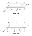
Referring to FIG. 8B , cross sections of yet another chip on lead packages according to the present invention are shown. In FIG. 8B , the package 86 includes a chip 12 attached to the leads 88 of a lead frame using a die attach film 54. Wires bonds 16 are provided to electrically couple bond pads on the die 12 to the leads 88. The package 80 is encapsulated is encapsulated in an encapsulant material 18. The leads 88 are bottom etched to create a gap region 89 under the die 12. With this embodiment, the purpose of bottom etching is to reduce the length of the foot print of the leads 88. By defining the length of the leads from 0.4 to 0.6 millimeters in length, the package 86 is complaint with the Jedec MO-220 and MO-229 standards.
Referring to FIGS. 8C and 8D , top and bottom views of a chip on lead package prior to encapsulation are shown. FIG. 8C shows the die 12 resting on the leads 88. Wire bonds 16 are used to electrically connect the bond pads (not shown) on the die to the leads 88. In FIG. 8D , the die 12 is again shown positioned on the leads 88. To increase the surface area upon which the die 12 is positioned, one or more of the leads 88 a and 88 b are extended as shown. For the sake of simplicity, the die attach film 54 is not shown in FIGS. 8C and 8D .
A leadless leadframe typically includes a plurality of die attach pads (PADs) arranged on the leadframe. A plurality of contacts are positioned around each PAD. The PADs and the contacts are held together by tie-bars. An adhesive tape is placed on the bottom of the leadframe, under the PADs and contacts. During the packaging process, a semiconductor chip is placed on each PAD using an adhesive or solder. Wire bonds are then formed between the chip and the contacts surrounding each chip. After wire bonding, the entire leadframe including the individual chips and wire bonds are encapsulated in a molding compound. The adhesive tape on the bottom of the leadframe is next removed, exposing the bottom surface of the PADs and the surrounding contacts. The leadframe is finally cut along the tie-bars, singulating the individual chip packages. The package is typically mounted by aligning the contacts of the package and soldering the bottom surface of the PAD to matching contacts on a printed circuit board. For more information on LLPs, see National Semiconductor's Application Note 1187 entitled “Leadless Leadframe Package (LLP)”, incorporated by reference herein for all purposes.
In spite of the fact that LLP packages do not have leads, the packages are still too large for many applications. As a consequence, packaging engineers are striving to make the packages thinner and to have a smaller footprint. One known approach to making the package smaller is to eliminate the PAD for each package. By doing so, the height of the package can be reduced. With this type of package, the chip is mounted onto the adhesive tape, wire bonded, and then encapsulated. The problem with this type of package is that the chip will often move relative to its surrounding contacts during encapsulation. This movement may cause the wire bonds to fail, resulting in low packaging yields. This type of package is therefore less than ideal.
An apparatus and method of making reliable miniature semiconductor packages having a reduced height and footprint is therefore needed.
To achieve the foregoing, and in accordance with the purpose of the present invention, a method and apparatus for making reliable miniature semiconductor packages having a reduced height and footprint is provided. The package includes a semiconductor chip having an active surface and a non-active surface and one or more contacts positioned adjacent the semiconductor chip. Electrical connections are formed between the contacts and the semiconductor chip. An adhesive tape provided adjacent the non-active surface of the semiconductor chip and the one or more contacts positioned adjacent the semiconductor chip. An adhesive material provided between the non-active surface of the chip and the adhesive tape.
The invention, together with further advantages thereof, may best be understood by reference to the following description taken in conjunction with the accompanying drawings in which:
In the Figures, like reference numbers refer to like components and elements.
Referring to FIG. 1 , a cross section of a semiconductor package according to one embodiment of the present invention is shown. The package 10 includes a semiconductor chip 12 having a top active surface 12 a and a non-active bottom surface 12 b. A plurality of contact leads 14 is provided surrounding the chip 12. Electrical connections 16, such as wire bonds, are provided between the leads 14 and I/O pads (not shown) on the active surface 12 a of the chip 12. The chip 12, leads 14 and wire bonds 16 are encapsulated in an encapsulant material 18, such as epoxy. An adhesive tape 20 is provided on the bottom surface of the package 10. An adhesive material 22 is provided between the non-active surface 12 b of the chip 12 and the tape 20. In various embodiments, the adhesive material 22 can be a non-conductive epoxy such as CRMX2154 from the Sumitomo Corporation of Japan or a conductive epoxy such as 8340 from Ablestik, which contains a silver resin. The adhesive material 22 is applied to either the tape 22 and/or the non-active surface 12 b of the chip 12 prior to encapsulation. The adhesive material 22 and the adhesive surface of the tape 20 cooperate together to prevent the chip 12 from moving or becoming misaligned relative to the leads 14 during encapsulation.
Referring to FIG. 2 , a cross section of another semiconductor package according to a second embodiment of the present invention is shown. The package 30 of FIG. 2 is similar to the package 10 as illustrated in FIG. 1 . As such, like elements are designated with like reference numbers and are not described in detail herein. The difference between the two packages 10 and 30, however, is that the adhesive material 22 is replaced with a another type of adhesive material 32, such as a double sided adhesive die-attach film. As illustrated in FIG. 2 , the adhesive material 32 is applied to the non-active surface 12 b of the chip 12. Again, the double-sided adhesive material 32 and the adhesive surface of the tape 20 cooperate together to prevent the chip 12 from moving or becoming misaligned relative to the leads 14 during encapsulation.
Referring to FIG. 3 , a perspective view of the application of adhesive material 32 onto a semiconductor wafer according to one embodiment of the present invention is shown. In this embodiment, the adhesive material 32 or die-attach film is applied to the chip 12 when in wafer form. As illustrated, the back surface of a wafer 34 is shown face up. The active surface of the wafer 34, with the chips 12 fabricated thereon, is face down and is therefore not visible in this view. Each of the chips 12 is separated on the wafer by horizontal and vertical scribe lines (not visible). After fabrication of the wafer 34 is complete, a sheet of the adhesive material 32 is adhered to the back or non-active surface of the wafer 34. Thereafter, the wafer 34 is cut along the horizontal and vertical scribe lines in accordance with standard semiconductor fabrication techniques, resulting in the singulation of the individual chips 12. In this case, each chip 12 includes the adhesive material 32 formed on the non-active surface 12 b of the chip 12 after singulation. In alternative embodiments, the adhesive material 32 can be applied individually to the non-active surface 12 b of each chip 12.
Referring to FIG. 4 , a flow chart 40 illustrating the manufacturing steps for making the semiconductor chip package of the present invention according to one embodiment is shown. In the initial step, the individual chips 12 are fabricated on the wafer 34 in accordance with standard semiconductor processing techniques (box 42). The adhesive material 22 or 32 is next applied to the non-active surface 12 b of the chips. As previously noted, an epoxy type adhesive material 22 can be applied to individual chips 12 after being signulated from the wafer 40. Alternatively, the epoxy can be applied to the adhesive tape 20 prior to placement of the chip 12 onto the tape. In yet another embodiment, the adhesive material such as the double stick die-attach film 32 can be applied to a wafer 40 and then singulated as discussed above (box 43) or applied individually to each chip 12. In the next step, the chip 12 is placed onto the tape 20 of the lead frame. As previously noted, the adhesive surface of the tape 20 and the adhesive material (either 22 or 32) cooperate together to securely hold the chip 12 in place (box 44). Thereafter, the chip 12 is wire bonded (box 45), and encapsulated (box 46). If more than one chip 12 is encapsulated on the lead frame, the chips are singulated (box 47) in the last step.
Referring to FIG. 6A , a leadframe 60 used for the chip on lead package 50 is shown. The leadframe 60 includes a plurality of tie-bars 62 which are used to hold the leads 52 for each package in place. The leads 52 are arranged to form a plurality of chip attach areas 64. The adhesive tape 20 is applied to the entire back surface of the leadframe 60 and is used to hold the leads 52 and the tie-bars 62 in place. During the packaging process, as illustrated in FIG. 6B , a chip 12 is secured to the leads 52 of an attach area 64. Although not visible in the figure, the adhesive tape 54 is used to secure the chip 12 to the leads 52 and the adhesive material, either an epoxy 22 or double-stick tape 32, is used to secure the chip 12 to the adhesive tape 20. Once the chip 12 is secured in place, it is encapsulated. For the sake of simplicity, only a single chip 12 and attach area 64 is shown. Typically though, chips 12 are placed on all the attach areas 64 and then the entire lead frame 60 is encapsulated. Thereafter, the lead frame 60 is cut along the tie-bars 64 to singulate each package.
Referring to FIGS. 7A and 7B , top and bottom perspective views of the package 50 are shown after singulation. In FIG. 7A , the chip 12 is encapsulated. As a result, only the encapsulating material 18 is visible. In FIG. 7B , however, the bottom view of the package 50 reveals the chip 12 overlapping and positioned over the leads 52. The chip on lead package 50 thus provides several advantages. A chip or die attach pad is not required. Accordingly, the height of the package 50 is reduced. Similarly, with the die resting on the leads 52, the lateral dimensions or “footprint” of the package is also reduced. Finally, the use of an adhesive between the chip 12, the tape 20, and the leads 52 tends to significantly reduce the possibility of the chip 12 moving out of alignment during the encapsulation process.
Referring to FIG. 8A , cross sections of another chip on lead packages according to the present invention are shown. In FIG. 8A , the package 80 includes a chip 12 attached to the leads 82 of a lead frame using a die attach film 54. Wires bonds 16 are provided to electrically couple bond pads on the die 12 to the leads 82. The package 80 is encapsulated is encapsulated in an encapsulant material 18. The leads 82 are top etched to reduce the thickness or height of the leads 84 in the die attach area. As a result, the overall height of the package 80.
Referring to FIG. 8B , cross sections of yet another chip on lead packages according to the present invention are shown. In FIG. 8B , the package 86 includes a chip 12 attached to the leads 88 of a lead frame using a die attach film 54. Wires bonds 16 are provided to electrically couple bond pads on the die 12 to the leads 82. The package 80 is encapsulated is encapsulated in an encapsulant material 18. The leads 82 are bottom etched to create a gap region under the die 12. With this embodiment, the purpose of bottom etching is to reduce the length of the foot print of the leads 88. By defining the length of the leads from 0.4 to 0.6 millimeters in length, the package 86 is complaint with the Jedec MO-220 and MO-229 standards.
Referring to FIGS. 8C and 8D , top and bottom views of a chip on lead package prior to encapsulation are shown. FIG. 8C shows the die 12 resting on the leads 52. Wire bonds 16 are used to electrically connect the bond pads (not shown) on the die to the leads 52. In FIG. 8D , the die 12 is again shown positioned on the leads 52. To increase the surface area upon which the die 12 is positioned, one or more of the leads 52 a and 52 b are extended as shown. For the sake of simplicity, the die attach film 54 is not shown in FIGS. 8C and 8D .
It should be noted that with the embodiments of FIGS. 5 , 8A and 8B, the die is attached to the leads or contacts of the package. In each example, wire bonds are used to electrically couple bond pads on the die to the lead contacts.
Although the foregoing invention has been described in some detail for purposes of clarity of understanding, it will be apparent that certain changes and modifications may be practiced within the scope of the appended claims. Therefore, the described embodiments should be taken as illustrative and not restrictive, and the invention should not be limited to the details given herein but should be defined by the following claims and their full scope of equivalents.
Claims (15)
1. An apparatus, comprising:
a semiconductor chip having an active surface and a non-active surface;
a plurality of contacts positioned adjacent the semiconductor chip, the plurality of contacts each having a first end of varying lengths respectively, the varying lets of the plurality of contacts provided under the semiconductor chip for providing a support surface for the semiconductor chip, the plurality of contacts entirely supporting the semiconductor chip without the use of a die attach pad;
electrical connections between the contacts and the semiconductor chip;
an adhesive tape provided adjacent the non-active surface of the semiconductor chip and the one or more contacts positioned adjacent the semiconductor chip; and
an adhesive material provided between and in direct contact with the non-active surface of the chip and the adhesive tape.
2. The apparatus of claim 1 , wherein the adhesive material is a non-conductive epoxy.
3. The apparatus of claim 1 , wherein the adhesive material is a conductive epoxy.
4. The apparatus if claim 3 , wherein the conductive epoxy contains a silver resin.
5. The apparatus of claim 1 , wherein the adhesive material is a double-stick tape applied to the non-active surface of the semiconductor device.
6. The apparatus of claim 1 , wherein the semiconductor chip rests upon the first end of the plurality of contacts.
7. The apparatus of claim 6 , wherein the adhesive material is a non-conductive tape positioned between the semiconductor chip and the one or more contacts.
8. The apparatus of claim 1 , further comprising an encapsulant material to encapsulate the semiconductor chip and one or more contacts.
9. The apparatus of claim 1 , wherein the contacts are leads.
10. The apparatus of claim 9 , wherein the semiconductor chip is supported on the leads.
11. The apparatus of claim 9 , wherein the leads are bottom etched.
12. The apparatus of claim 9 , wherein the leads are top etched.
13. An apparatus, comprising:
one or more leads, the one or more leads each having a first end of varying lengths respectively;
a semiconductor chip having an active surface and a non-active surface, the non-active surface of the semiconductor chip being supported by the varying lengths of the first end of the one or more leads respectively, the semiconductor chip being entirely supported on the one or more leads without a die attach pad;
a non-conductive material positioned between and directly in contact with both the non-active surface of the semiconductor chip and the one or more leads; and
an adhesive tape on the non-conductive material, the adhesive tape acting to adhere the semiconductor chin onto the one or more leads.
14. The apparatus of claim 13 , wherein the adhesive material is a non-conductive epoxy.
15. The apparatus of clam 13, wherein the adhesive material is a conductive epoxy.
Priority Applications (2)
| Application Number | Priority Date | Filing Date | Title |
|---|---|---|---|
| US10/942,061 US7161232B1 (en) | 2004-09-14 | 2004-09-14 | Apparatus and method for miniature semiconductor packages |
| US11/607,141 US7419855B1 (en) | 2004-09-14 | 2006-12-01 | Apparatus and method for miniature semiconductor packages |
Applications Claiming Priority (1)
| Application Number | Priority Date | Filing Date | Title |
|---|---|---|---|
| US10/942,061 US7161232B1 (en) | 2004-09-14 | 2004-09-14 | Apparatus and method for miniature semiconductor packages |
Related Child Applications (1)
| Application Number | Title | Priority Date | Filing Date |
|---|---|---|---|
| US11/607,141 Division US7419855B1 (en) | 2004-09-14 | 2006-12-01 | Apparatus and method for miniature semiconductor packages |
Publications (1)
| Publication Number | Publication Date |
|---|---|
| US7161232B1 true US7161232B1 (en) | 2007-01-09 |
Family
ID=37633463
Family Applications (2)
| Application Number | Title | Priority Date | Filing Date |
|---|---|---|---|
| US10/942,061 Active US7161232B1 (en) | 2004-09-14 | 2004-09-14 | Apparatus and method for miniature semiconductor packages |
| US11/607,141 Active 2024-11-01 US7419855B1 (en) | 2004-09-14 | 2006-12-01 | Apparatus and method for miniature semiconductor packages |
Family Applications After (1)
| Application Number | Title | Priority Date | Filing Date |
|---|---|---|---|
| US11/607,141 Active 2024-11-01 US7419855B1 (en) | 2004-09-14 | 2006-12-01 | Apparatus and method for miniature semiconductor packages |
Country Status (1)
| Country | Link |
|---|---|
| US (2) | US7161232B1 (en) |
Cited By (10)
| Publication number | Priority date | Publication date | Assignee | Title |
|---|---|---|---|---|
| US20070170554A1 (en) * | 2006-01-23 | 2007-07-26 | Stats Chippac Ltd. | Integrated circuit package system with multiple molding |
| US20070170555A1 (en) * | 2006-01-23 | 2007-07-26 | Camacho Zigmund R | Padless die support integrated circuit package system |
| US7419855B1 (en) * | 2004-09-14 | 2008-09-02 | National Semiconductor Corporation | Apparatus and method for miniature semiconductor packages |
| US20090072366A1 (en) * | 2007-09-18 | 2009-03-19 | Guruprasad Badakere Govindaiah | Integrated circuit package system with dual connectivity |
| US20090079049A1 (en) * | 2007-09-20 | 2009-03-26 | Byung Tai Do | Integrated circuit package system with warp-free chip |
| US20100006993A1 (en) * | 2008-07-11 | 2010-01-14 | Arnel Senosa Trasporto | Integrated circuit package system with chip on lead |
| US20100072589A1 (en) * | 2008-09-22 | 2010-03-25 | Zigmund Ramirez Camacho | Semiconductor package system with die support pad |
| US20100123227A1 (en) * | 2008-11-17 | 2010-05-20 | Frederick Rodriguez Dahilig | Integrated circuit packaging system with increased connectivity and method of manufacture thereof |
| US20100219518A1 (en) * | 2009-02-27 | 2010-09-02 | Advanced Semiconductor Engineering, Inc. | Quad flat non-leaded package |
| US20160163623A1 (en) * | 2012-05-31 | 2016-06-09 | Freescale Semiconductor, Inc. | System, method and apparatus for leadless surface mounted semiconductor package |
Families Citing this family (5)
| Publication number | Priority date | Publication date | Assignee | Title |
|---|---|---|---|---|
| JP2011517069A (en) * | 2009-03-06 | 2011-05-26 | カイシン インコーポレイテッド | Leadless integrated circuit package with high density contacts |
| WO2010111885A1 (en) | 2009-04-03 | 2010-10-07 | Kaixin, Inc. | Leadframe for ic package and method of manufacture |
| US20100314728A1 (en) * | 2009-06-16 | 2010-12-16 | Tung Lok Li | Ic package having an inductor etched into a leadframe thereof |
| WO2011026261A1 (en) | 2009-09-02 | 2011-03-10 | Tunglok Li | Ic package and method for manufacturing the same |
| US20110248392A1 (en) * | 2010-04-12 | 2011-10-13 | Texas Instruments Incorporated | Ball-Grid Array Device Having Chip Assembled on Half-Etched metal Leadframe |
Citations (19)
| Publication number | Priority date | Publication date | Assignee | Title |
|---|---|---|---|---|
| US4480013A (en) * | 1981-07-20 | 1984-10-30 | Sumitomo Electric Industries, Ltd. | Substrate for use in semiconductor apparatus |
| US4550333A (en) * | 1983-09-13 | 1985-10-29 | Xerox Corporation | Light emitting semiconductor mount |
| US5175060A (en) * | 1989-07-01 | 1992-12-29 | Ibiden Co., Ltd. | Leadframe semiconductor-mounting substrate having a roughened adhesive conductor circuit substrate and method of producing the same |
| US5304843A (en) * | 1990-06-01 | 1994-04-19 | Kabushiki Kaisha Toshiba | Semiconductor device using film carrier |
| US5471088A (en) * | 1992-11-07 | 1995-11-28 | Goldstar Electron Co., Ltd. | Semiconductor package and method for manufacturing the same |
| US5614316A (en) * | 1995-06-08 | 1997-03-25 | Tomoegawa Paper Co., Ltd. | Adhesive tape for electronic parts and liquid adhesive |
| JPH09283661A (en) * | 1996-04-19 | 1997-10-31 | Toshiba Corp | Resin-sealed semiconductor device |
| US5818105A (en) * | 1994-07-22 | 1998-10-06 | Nec Corporation | Semiconductor device with plastic material covering a semiconductor chip mounted on a substrate of the device |
| US5859471A (en) * | 1992-11-17 | 1999-01-12 | Shinko Electric Industries Co., Ltd. | Semiconductor device having tab tape lead frame with reinforced outer leads |
| US5866939A (en) * | 1996-01-21 | 1999-02-02 | Anam Semiconductor Inc. | Lead end grid array semiconductor package |
| JPH11260972A (en) * | 1998-03-13 | 1999-09-24 | Sumitomo Metal Mining Co Ltd | Thin semiconductor device |
| US6132865A (en) * | 1997-07-23 | 2000-10-17 | Tomoegawa Paper Co., Ltd. | Adhesive tape for electronic parts |
| US6265782B1 (en) * | 1996-10-08 | 2001-07-24 | Hitachi Chemical Co., Ltd. | Semiconductor device, semiconductor chip mounting substrate, methods of manufacturing the device and substrate, adhesive, and adhesive double coated film |
| US6281568B1 (en) * | 1998-10-21 | 2001-08-28 | Amkor Technology, Inc. | Plastic integrated circuit device package and leadframe having partially undercut leads and die pad |
| US6294100B1 (en) | 1998-06-10 | 2001-09-25 | Asat Ltd | Exposed die leadless plastic chip carrier |
| US6300673B1 (en) * | 1992-08-21 | 2001-10-09 | Advanced Interconnect Technologies, Inc. | Edge connectable metal package |
| JP2002184801A (en) * | 2000-10-02 | 2002-06-28 | Nitto Denko Corp | Method of manufacturing semiconductor device |
| US6429508B1 (en) * | 2000-08-09 | 2002-08-06 | Kostat Semiconductor Co., Ltd. | Semiconductor package having implantable conductive lands and method for manufacturing the same |
| US6673441B1 (en) * | 1999-06-18 | 2004-01-06 | Hitachi Chemical Company, Ltd. | Adhesive, adhesive member, interconnecting substrate for semiconductor mounting having adhesive member, and semiconductor device containing the same |
Family Cites Families (3)
| Publication number | Priority date | Publication date | Assignee | Title |
|---|---|---|---|---|
| JPH08306853A (en) * | 1995-05-09 | 1996-11-22 | Fujitsu Ltd | Semiconductor device, manufacture thereof and manufacture of lead frame |
| US6201292B1 (en) * | 1997-04-02 | 2001-03-13 | Dai Nippon Insatsu Kabushiki Kaisha | Resin-sealed semiconductor device, circuit member used therefor |
| US7161232B1 (en) * | 2004-09-14 | 2007-01-09 | National Semiconductor Corporation | Apparatus and method for miniature semiconductor packages |
-
2004
- 2004-09-14 US US10/942,061 patent/US7161232B1/en active Active
-
2006
- 2006-12-01 US US11/607,141 patent/US7419855B1/en active Active
Patent Citations (19)
| Publication number | Priority date | Publication date | Assignee | Title |
|---|---|---|---|---|
| US4480013A (en) * | 1981-07-20 | 1984-10-30 | Sumitomo Electric Industries, Ltd. | Substrate for use in semiconductor apparatus |
| US4550333A (en) * | 1983-09-13 | 1985-10-29 | Xerox Corporation | Light emitting semiconductor mount |
| US5175060A (en) * | 1989-07-01 | 1992-12-29 | Ibiden Co., Ltd. | Leadframe semiconductor-mounting substrate having a roughened adhesive conductor circuit substrate and method of producing the same |
| US5304843A (en) * | 1990-06-01 | 1994-04-19 | Kabushiki Kaisha Toshiba | Semiconductor device using film carrier |
| US6300673B1 (en) * | 1992-08-21 | 2001-10-09 | Advanced Interconnect Technologies, Inc. | Edge connectable metal package |
| US5471088A (en) * | 1992-11-07 | 1995-11-28 | Goldstar Electron Co., Ltd. | Semiconductor package and method for manufacturing the same |
| US5859471A (en) * | 1992-11-17 | 1999-01-12 | Shinko Electric Industries Co., Ltd. | Semiconductor device having tab tape lead frame with reinforced outer leads |
| US5818105A (en) * | 1994-07-22 | 1998-10-06 | Nec Corporation | Semiconductor device with plastic material covering a semiconductor chip mounted on a substrate of the device |
| US5614316A (en) * | 1995-06-08 | 1997-03-25 | Tomoegawa Paper Co., Ltd. | Adhesive tape for electronic parts and liquid adhesive |
| US5866939A (en) * | 1996-01-21 | 1999-02-02 | Anam Semiconductor Inc. | Lead end grid array semiconductor package |
| JPH09283661A (en) * | 1996-04-19 | 1997-10-31 | Toshiba Corp | Resin-sealed semiconductor device |
| US6265782B1 (en) * | 1996-10-08 | 2001-07-24 | Hitachi Chemical Co., Ltd. | Semiconductor device, semiconductor chip mounting substrate, methods of manufacturing the device and substrate, adhesive, and adhesive double coated film |
| US6132865A (en) * | 1997-07-23 | 2000-10-17 | Tomoegawa Paper Co., Ltd. | Adhesive tape for electronic parts |
| JPH11260972A (en) * | 1998-03-13 | 1999-09-24 | Sumitomo Metal Mining Co Ltd | Thin semiconductor device |
| US6294100B1 (en) | 1998-06-10 | 2001-09-25 | Asat Ltd | Exposed die leadless plastic chip carrier |
| US6281568B1 (en) * | 1998-10-21 | 2001-08-28 | Amkor Technology, Inc. | Plastic integrated circuit device package and leadframe having partially undercut leads and die pad |
| US6673441B1 (en) * | 1999-06-18 | 2004-01-06 | Hitachi Chemical Company, Ltd. | Adhesive, adhesive member, interconnecting substrate for semiconductor mounting having adhesive member, and semiconductor device containing the same |
| US6429508B1 (en) * | 2000-08-09 | 2002-08-06 | Kostat Semiconductor Co., Ltd. | Semiconductor package having implantable conductive lands and method for manufacturing the same |
| JP2002184801A (en) * | 2000-10-02 | 2002-06-28 | Nitto Denko Corp | Method of manufacturing semiconductor device |
Non-Patent Citations (1)
| Title |
|---|
| National Semiconductor Corporation, "Leadless Leadframe Package (LLP)" AN-1187, Mar. 2004, 21 pages. |
Cited By (25)
| Publication number | Priority date | Publication date | Assignee | Title |
|---|---|---|---|---|
| US7419855B1 (en) * | 2004-09-14 | 2008-09-02 | National Semiconductor Corporation | Apparatus and method for miniature semiconductor packages |
| US7871863B2 (en) | 2006-01-23 | 2011-01-18 | Stats Chippac Ltd. | Integrated circuit package system with multiple molding |
| US20070170555A1 (en) * | 2006-01-23 | 2007-07-26 | Camacho Zigmund R | Padless die support integrated circuit package system |
| US7449369B2 (en) | 2006-01-23 | 2008-11-11 | Stats Chippac Ltd. | Integrated circuit package system with multiple molding |
| US20090014849A1 (en) * | 2006-01-23 | 2009-01-15 | Zigmund Ramirez Camacho | Integrated circuit package system with multiple molding |
| US8629537B2 (en) | 2006-01-23 | 2014-01-14 | Stats Chippac Ltd. | Padless die support integrated circuit package system |
| US20070170554A1 (en) * | 2006-01-23 | 2007-07-26 | Stats Chippac Ltd. | Integrated circuit package system with multiple molding |
| US20090072366A1 (en) * | 2007-09-18 | 2009-03-19 | Guruprasad Badakere Govindaiah | Integrated circuit package system with dual connectivity |
| US8120150B2 (en) | 2007-09-18 | 2012-02-21 | Stats Chippac Ltd. | Integrated circuit package system with dual connectivity |
| US7892894B2 (en) | 2007-09-20 | 2011-02-22 | Stats Chippac Ltd. | Method of manufacturing integrated circuit package system with warp-free chip |
| US20090079049A1 (en) * | 2007-09-20 | 2009-03-26 | Byung Tai Do | Integrated circuit package system with warp-free chip |
| US8421197B2 (en) | 2007-09-20 | 2013-04-16 | Stats Chippac Ltd. | Integrated circuit package system with warp-free chip |
| US20110121466A1 (en) * | 2007-09-20 | 2011-05-26 | Byung Tai Do | Integrated circuit package system with warp-free chip |
| US20100006993A1 (en) * | 2008-07-11 | 2010-01-14 | Arnel Senosa Trasporto | Integrated circuit package system with chip on lead |
| US8269324B2 (en) | 2008-07-11 | 2012-09-18 | Stats Chippac Ltd. | Integrated circuit package system with chip on lead |
| US7911067B2 (en) | 2008-09-22 | 2011-03-22 | Stats Chippac Ltd. | Semiconductor package system with die support pad |
| US20110129965A1 (en) * | 2008-09-22 | 2011-06-02 | Zigmund Ramirez Camacho | Method for manufacturing semiconductor package system with die support pad |
| US8216883B2 (en) | 2008-09-22 | 2012-07-10 | Stats Chippac Ltd | Method for manufacturing semiconductor package system with die support pad |
| US20100072589A1 (en) * | 2008-09-22 | 2010-03-25 | Zigmund Ramirez Camacho | Semiconductor package system with die support pad |
| US8022539B2 (en) | 2008-11-17 | 2011-09-20 | Stats Chippac Ltd. | Integrated circuit packaging system with increased connectivity and method of manufacture thereof |
| US20100123227A1 (en) * | 2008-11-17 | 2010-05-20 | Frederick Rodriguez Dahilig | Integrated circuit packaging system with increased connectivity and method of manufacture thereof |
| US20100219518A1 (en) * | 2009-02-27 | 2010-09-02 | Advanced Semiconductor Engineering, Inc. | Quad flat non-leaded package |
| TWI382503B (en) * | 2009-02-27 | 2013-01-11 | Advanced Semiconductor Eng | Quad flat non-leaded package |
| US8957506B2 (en) * | 2009-02-27 | 2015-02-17 | Advanced Semiconductor Engineering, Inc. | Quad flat non-leaded package |
| US20160163623A1 (en) * | 2012-05-31 | 2016-06-09 | Freescale Semiconductor, Inc. | System, method and apparatus for leadless surface mounted semiconductor package |
Also Published As
| Publication number | Publication date |
|---|---|
| US7419855B1 (en) | 2008-09-02 |
Similar Documents
| Publication | Publication Date | Title |
|---|---|---|
| US7419855B1 (en) | Apparatus and method for miniature semiconductor packages | |
| US7378298B2 (en) | Method of making stacked die package | |
| US6452255B1 (en) | Low inductance leadless package | |
| JP3420057B2 (en) | Resin-sealed semiconductor device | |
| US7371608B2 (en) | Method of fabricating a stacked die having a recess in a die BGA package | |
| CN101512762B (en) | Stackable packages for three-dimensional packaging of semiconductor dice | |
| US8836101B2 (en) | Multi-chip semiconductor packages and assembly thereof | |
| US7595551B2 (en) | Semiconductor package for a large die | |
| US6936929B1 (en) | Multichip packages with exposed dice | |
| KR101037246B1 (en) | Multi Chip Leadframe Package | |
| US6723585B1 (en) | Leadless package | |
| US7288439B1 (en) | Leadless microelectronic package and a method to maximize the die size in the package | |
| US8093694B2 (en) | Method of manufacturing non-leaded integrated circuit package system having etched differential height lead structures | |
| US20050127491A1 (en) | Stacked die semiconductor device | |
| US20070176269A1 (en) | Multi-chips module package and manufacturing method thereof | |
| US20120217657A1 (en) | Multi-chip module package | |
| US6869824B2 (en) | Fabrication method of window-type ball grid array semiconductor package | |
| US7642638B2 (en) | Inverted lead frame in substrate | |
| US20200343168A1 (en) | Lead stabilization in semiconductor packages | |
| US6576988B2 (en) | Semiconductor package | |
| US20040036151A1 (en) | Double leadframe-based packaging structure and manufacturing process thereof | |
| KR100891649B1 (en) | Method of manufacturing semiconductor package | |
| US20080038872A1 (en) | Method of manufacturing semiconductor device | |
| JP2001284370A (en) | Method of manufacturing semiconductor device | |
| KR20090098074A (en) | Method of fabricating stack package |
Legal Events
| Date | Code | Title | Description |
|---|---|---|---|
| AS | Assignment |
Owner name: NATIONAL SEMICONDUCTOR CORPORATION, CALIFORNIA Free format text: ASSIGNMENT OF ASSIGNORS INTEREST;ASSIGNORS:LEE, SHAW WEI;TU, NGHIA THUC;S/O NADARAJAH, SANTHIRAN;AND OTHERS;REEL/FRAME:015582/0822;SIGNING DATES FROM 20040907 TO 20041215 |
|
| STCF | Information on status: patent grant |
Free format text: PATENTED CASE |
|
| CC | Certificate of correction | ||
| FPAY | Fee payment |
Year of fee payment: 4 |
|
| FPAY | Fee payment |
Year of fee payment: 8 |
|
| MAFP | Maintenance fee payment |
Free format text: PAYMENT OF MAINTENANCE FEE, 12TH YEAR, LARGE ENTITY (ORIGINAL EVENT CODE: M1553) Year of fee payment: 12 |