US7158633B1 - Method and apparatus for monitoring subscriber loop interface circuitry power dissipation - Google Patents
Method and apparatus for monitoring subscriber loop interface circuitry power dissipation Download PDFInfo
- Publication number
- US7158633B1 US7158633B1 US09/441,380 US44138099A US7158633B1 US 7158633 B1 US7158633 B1 US 7158633B1 US 44138099 A US44138099 A US 44138099A US 7158633 B1 US7158633 B1 US 7158633B1
- Authority
- US
- United States
- Prior art keywords
- tip
- ring
- linefeed
- subscriber loop
- line
- Prior art date
- Legal status (The legal status is an assumption and is not a legal conclusion. Google has not performed a legal analysis and makes no representation as to the accuracy of the status listed.)
- Expired - Fee Related
Links
Images


Classifications
-
- H—ELECTRICITY
- H04—ELECTRIC COMMUNICATION TECHNIQUE
- H04M—TELEPHONIC COMMUNICATION
- H04M19/00—Current supply arrangements for telephone systems
Definitions
- This invention relates to the field of telecommunications.
- this invention is drawn to subscriber loop interface circuitry.
- Subscriber line interface circuits are typically found in the central office exchange of a telecommunications network.
- a subscriber line interface circuit (SLIC) provides a communications interface between the digital switching network of a central office and an analog subscriber line.
- the analog subscriber line connects to a subscriber station or telephone instrument at a location remote from the central office exchange.
- the analog subscriber line and subscriber equipment form a subscriber loop.
- the interface requirements of an SLIC typically result in the need to provide relatively high voltages and currents for control signaling with respect to the subscriber equipment on the subscriber loop.
- Voiceband communications are typically low voltage analog signals on the subscriber loop.
- the SLIC must detect and transform low voltage analog signals into digital data for transmitting communications received from the subscriber equipment to the digital network.
- the SLIC must also transform digital data received from the digital network into low voltage analog signals for transmission on the subscriber loop to the subscriber equipment.
- One SLIC design includes discrete passive inductive components such as transformers for handling the higher voltages and currents. Disadvantages of this design include the bulkiness, weight, and power consumption of the passive inductive components.
- Another SLIC design incorporates multiple specialized integrated circuits to achieve a transformerless SLIC. Typically one integrated circuit is dedicated to handling the low voltage digital signaling and another integrated circuit is dedicated to handling the higher powered analog control signaling functions required for the subscriber loop.
- One disadvantage of this design is that programming of various SLIC operational characteristics is typically accomplished using discrete components such that the SLIC operational characteristics are not dynamically modifiable.
- the integrated circuit handling the higher powered analog control signaling functions tends to be relatively expensive.
- the subscriber line interface circuitry includes an integrated circuit having sense inputs for a sensed tip signal and a sensed ring signal of a subscriber loop.
- the integrated circuit generates a subscriber loop linefeed driver control signal in response to the sensed signals.
- the linefeed driver does not reside with the integrated circuit.
- a method for monitoring power dissipation of the linefeed driver components includes the step of sampling at least one of a tip and a ring signal to determine a line voltage and a line current of a linefeed component of the subscriber loop. An instantaneous power dissipation of the linefeed component is estimated. The estimated instantaneous power dissipation is filtered to generate an estimated junction temperature of the linefeed component.
- An apparatus for monitoring power dissipation of a selected linefeed component includes an analog-to-digital converter (ADC) for providing a sampled value from at least one of a tip and a ring line.
- a power calculator calculates an instantaneous power dissipation of the selected linefeed component from the sampled value and control currents provided to a plurality of linefeed driver components.
- a filter provides an estimated junction temperature of the selected linefeed component from the instantaneous power dissipation.
- a subscriber loop interface circuit includes a signal processor with sense inputs for sensing a tip line and a ring line of the subscriber loop.
- the signal processor generates subscriber loop control signals in response to the sensed inputs.
- a linefeed driver drives the subscriber loop in accordance with the subscriber loop control signals.
- the linefeed driver includes a tip fuse series-coupled to a tip resistor and the tip line and a ring fuse series-coupled to a ring resistor and the ring line. Voltages sampled from each side of the series-coupled tip fuse and resistor collectively form the sensed tip signal. Voltages sampled from each side of the series-coupled ring fuse and resistor collectively form the sensed ring signal.
- sensing of the tip and ring lines for subscriber loop control can be accomplished across components including tip or ring inline protective devices such as fuses such that one lead of a pair of sense leads is unprotected by the fuse and the other lead is protected by the fuse.
- tip or ring inline protective devices such as fuses
- This enables using the same sensing circuitry for power monitoring as well as to determine other line conditions such as whether the fuses are blown without the use of separate sensing circuitry dedicated to that purpose.
- This approach reduces the number of pins on an integrated circuit needed to monitor power dissipation and determine pre-fuse line conditions.
- FIG. 1 illustrates one embodiment of a central office exchange including a subscriber line interface circuit (SLIC) coupling subscriber equipment to a digital switching system.
- SLIC subscriber line interface circuit
- FIG. 2 illustrates a block diagram of an SLIC including a signal processor and a linefeed driver.
- FIG. 3 illustrates one embodiment of an SLIC linefeed driver.
- FIG. 4 illustrates a block diagram of an alternative embodiment of the SLIC.
- FIG. 5 illustrates power monitoring circuitry within the signal processor.
- FIG. 6 illustrates a method for monitoring power dissipation of a selected linefeed driver component.
- FIG. 7 illustrates one embodiment of the subscriber line interface circuit wherein at least one of each of the tip and ring sense lines is coupled to the unprotected side of a fused subscriber loop circuit.
- FIG. 1 illustrates functional elements of one embodiment of a subscriber line interface circuit (SLIC) 110 typically associated with plain old telephone services (POTS) telephone lines.
- SLIC subscriber line interface circuit
- POTS plain old telephone services
- the subscriber line interface circuit (SLIC) provides an interface between a digital switching network 120 of a local telephone company central exchange and a subscriber loop 132 including subscriber equipment 130 .
- the subscriber loop 132 is typically used for communicating analog data signals (e.g., voiceband communications) as well as subscriber loop “handshaking” or control signals.
- the analog data signals are typically on the order of 1 volt peak-to-peak (i.e., “small signal”).
- the subscriber loop control signals typically consist of a 48 V d.c. offset and an a.c. signal of 40–140 Vrms (i.e., “large signal”).
- the subscriber loop state is often specified in terms of the tip 180 and ring 190 portions of the subscriber loop.
- BORSCHT is an acronym for “battery feed,” “overvoltage protection,” “ring,” “supervision,” “codec,” “hybrid,” and “test.”
- the SLIC provides power to the subscriber equipment 180 using the battery feed function.
- the overvoltage protection function serves to protect the central office circuitry against voltage transients that may occur on the subscriber loop 132 .
- the ring function enables the SLIC to signal the subscriber equipment 180 .
- subscriber equipment 180 is a telephone.
- the ring function enables the SLIC to ring the telephone.
- the supervision function enables the SLIC to detect service requests such as when the caller goes off-hook.
- the supervision function is also used to supervise calls in progress and to detect dialing input signals.
- the hybrid function provides a conversion from two wire signaling to four wire signaling.
- the SLIC includes a codec to convert the four-wire analog voiceband data signal into serial digital codes suitable for transmission by the digital switching network 120 .
- pulse code modulation is used to encode the voiceband data.
- the SLIC also typically provides a means to test for or to indicate faults that may exist in the subscriber loop or the SLIC itself.
- the codec function has relatively low power requirements and can be implemented in a low voltage integrated circuit operating in the range of approximately 5 volts or less.
- the battery feed and supervision circuitry typically operate in the range of 40–75 volts.
- the ringing function is handled by the same circuitry as the battery feed and supervision circuitry.
- the ringing function is performed by higher voltage ringing circuitry (75–150 V rms ).
- the ringing function as well as the overvoltage protection function may be associated with circuitry having greater voltage or current operating requirements than the other circuitry.
- Recent transformerless SLIC designs tend to distribute the functional requirements between two integrated circuits based on whether the functions are traditionally associated with the high voltage subscriber loop controls or the low voltage data processing.
- the codec is implemented in a low voltage integrated circuit and the remaining functions (e.g., supervision) are implemented primarily in a high voltage integrated circuit such as a bipolar integrated circuit.
- this design tends to offer considerable space, weight, and power efficiencies over designs requiring passive inductive components, this distribution of the functional requirements tends to result in a relatively expensive high voltage integrated circuit.
- FIG. 2 illustrates one embodiment of an SLIC 200 wherein the BORSCHT functions have been redistributed between a signal processor 210 and a linefeed driver 220 .
- Signal processor 210 is responsible for at least the ring control, supervision, codec, and hybrid functions.
- Signal processor 210 controls and interprets the large signal subscriber loop control signals as well as handling the small signal analog voiceband data and the digital voiceband data.
- signal processor 210 is an integrated circuit.
- the integrated circuit includes sense inputs for a sensed tip and ring signal of the subscriber loop.
- the integrated circuit generates subscriber loop linefeed driver control signal in response to the sensed signals.
- the linefeed driver does not reside within the integrated circuit or within the same integrated circuit package as the signal processor 210 .
- Signal processor 210 receives subscriber loop state information from linefeed driver 220 as indicated by tip/ring sense 222 . This information is used to generate control signals for linefeed driver 220 as indicated by linefeed driver control 212 .
- the voiceband 230 signal is used for bi-directional communication of the analog voiceband data between linefeed driver 220 and signal processor 210 .
- Signal processor 210 includes a digital interface for communicating digitized voiceband data to the digital switching network using digital voiceband 216 .
- the digital interface includes a processor interface 214 to enable programmatic control of the signal processor 210 .
- the processor interface effectively enables programmatic or dynamic control of battery control, battery feed state control, voiceband data amplification and level shifting, longitudinal balance, ringing currents, and other subscriber loop control parameters as well as setting thresholds such as a ring trip detection thresholds and an off-hook detection threshold.
- the digital voiceband data 214 is coupled to a digital codec interface of signal processor 210 for bi-directional communication of the digital voiceband data between the codec of the signal processor and the digital switching network.
- the analog voiceband data 230 is coupled to an analog codec interface of signal processor 210 for bi-directional communication of the analog voiceband data between the codec and the linefeed driver.
- Linefeed driver 220 maintains responsibility for battery feed to tip 280 and ring 290 . Overvoltage protection is not explicitly illustrated, however, overvoltage protection can be provided by fuses incorporated into linefeed driver 220 , if desired.
- Linefeed driver 220 includes sense circuitry to provide signal processor 210 with pre-determined sensed subscriber loop operating parameters as indicated by tip/ring sense 222 . Signal processor 210 performs any necessary processing on the sensed parameters in order to determine the operational state of the subscriber loop. For example, differences or sums of sensed voltages and currents are performed as necessary by signal processor 210 rather than linefeed driver 220 . Thus common mode and differential mode components (e.g., voltage and current) of the subscriber loop are calculated by the signal processor rather than the linefeed driver.
- common mode and differential mode components e.g., voltage and current
- Linefeed driver 220 modifies the large signal tip and ring operating conditions in response to linefeed driver control 212 provided by signal processor 210 .
- This arrangement enables the signal processor to perform processing as needed to handle the majority of the BORSCHT functions. For example, the supervisory functions of ring trip, ground key, and off-hook detection can be determined by signal processor 210 based on operating parameters provided by tip/ring sense 222 .
- FIG. 3 illustrates one embodiment of an SLIC linefeed driver 300 .
- the linefeed driver 300 is implemented as a number of discrete components.
- Linefeed driver 300 includes a voiceband circuitry 320 , sensing circuitry 330 , and power circuitry 340 .
- Voiceband circuitry 320 enables data signals corresponding to voiceband communications to be retrieved from or impressed onto the subscriber loop.
- Capacitors CR and CT effectively provide a.c. coupling for the analog voiceband data from the subscriber loop to the signal processor while decoupling signal processor 210 from the d.c. offsets of the tip 380 and ring 390 nodes.
- capacitors CR and CT effective provide d.c. isolation of the analog voiceband data interface formed by nodes 322 – 328 from the subscriber loop.
- voiceband circuitry 320 provides a.c. coupling of the analog voiceband data between the subscriber loop and the signal processor using only passive components.
- Voiceband communication is bi-directional between the subscriber loop and signal processor 210 .
- Nodes 324 and 328 serve to communicate voiceband data from the subscriber loop to signal processor 210 (i.e., tip and ring “audio in”).
- Nodes 322 and 326 provide a means of impressing a signal on the subscriber loop from signal processor 210 (i.e., tip and ring “audio out”).
- RTT and RTR collectively establish a 600 ⁇ termination impedance.
- Sensing circuitry 330 enables signal processor 210 to determine the tip 380 and ring 390 node voltages as well as the subscriber loop current using sensing resistors RS 1 , RS 2 , RS 3 , and RS 4 . Resistors RT and RR are used to generate a voltage drop for determining the tip and ring currents. In one embodiment, sensing circuitry 330 consists only of passive discrete components.
- tip/ring sense 222 includes a sensed tip signal and a sensed ring signal.
- the sensed tip signal includes first and second sampled tip voltages.
- Resistors RS 1 and RS 2 are used to sample the tip line voltage at each end of RT.
- Resistors RS 1 and RS 2 convert the sampled tip line voltages to currents suitable for handling by signal processor 210 at nodes 332 and 334 .
- the difference between the first and second sampled tip voltages is proportional to the tip current.
- the sensed ring signal includes first and second sampled ring voltages.
- Resistors RS 3 and RS 4 similarly convert sampled ring line voltages at both ends of RR to currents suitable for handling by signal processor 210 at nodes 336 and 338 .
- the difference between the first and second sampled ring voltages is proportional to the ring current.
- Power circuitry 340 provides the battery feed and other relatively high voltage functions to the subscriber loop in accordance with analog linefeed control signals provided by the signal processor 210 at nodes 342 , 344 , 346 , and 348 . Processing of the sensed parameters of the tip and ring lines for generating the linefeed control signals is handled exclusively by signal processor 210 .
- the subscriber loop current and the tip and ring voltages are controlled by transistors Q 1 –Q 6 .
- Q 1 –Q 4 are PNP bipolar junction transistors and Q 5 –Q 6 are NPN bipolar junction transistors. Given that the base terminals of Q 1 –Q 4 are coupled to ground, nodes 342 – 348 need only be approximately 0.7 volts to turn on transistors Q 1 –Q 4 . Due to the small voltage drop between the base and emitters of Q 1 –Q 4 , control of the linefeed circuitry requires relatively low power and thus linefeed driver control currents I 1 –I 4 may be provided by a signal processor 210 implemented as a low voltage complementary metal oxide semiconductor (CMOS) integrated circuit.
- CMOS complementary metal oxide semiconductor
- Transistors Q 1 , Q 4 , and Q 6 control the tip voltage 380 .
- the tip voltage is increased by the application of control current I 1 to Q 1 .
- the tip voltage (node 380 ) is decreased by the application of control current I 4 to Q 4 .
- control currents I 1 and I 4 effectively provide a tip control signal for manipulating the tip voltage at node 380 .
- transistors Q 2 , Q 3 , and Q 5 (and resistor R 1 ) control the ring voltage 390 .
- the application of control current I 3 to Q 3 increases the ring voltage.
- the ring voltage is decreased by the application of control current I 2 to Q 2 .
- Control currents I 2 and I 3 effectively provide a ring control signal for manipulating the ring voltage at node 390 .
- Control currents I 1 –I 4 thus effectively control the large signal subscriber loop current and tip and ring voltages.
- the ringing signal can be generated by using the control signals at nodes 342 – 348 to periodically reverse the polarity of tip 380 with respect to ring 390 (i.e., battery polarity reversal) at the nominal ringing frequency.
- Sensing portion 330 enables signal processor 210 to determine the large signal state of the subscriber loop without the need for intervening active circuitry or level shifters.
- sensing portion 330 comprises only passive discrete components.
- the linefeed control inputs 342 – 348 enable signal processor 210 to actively manage the large signal state of the subscriber loop.
- the large signal a.c. and d.c. components of the subscriber loop control protocol can now be controlled directly by a low voltage integrated circuit.
- the large signal a.c. and d.c. control loops are effectively terminated at the signal processor 210 .
- the large signal a.c. and d.c. control loops are terminated at the low voltage integrated circuit.
- signal processing and state determination such as off-hook, ring trip, and ring control formerly associated with high power analog circuitry can be handled predominately by a low voltage integrated circuit.
- the integrated circuit signal processor can handle processing of the small signal analog voiceband data from the subscriber loop without the need for intervening active elements or level shifting circuitry.
- FIG. 4 illustrates a block diagram of an alternative embodiment of an SLIC. Comparing FIG. 4 with FIG. 2 , the primary difference is that a portion of the voiceband communication function ( 230 ) is handled by the same signal lines handling the linefeed driver control ( 212 ). In particular, signal lines 412 combine the linefeed driver control function with transmission of voiceband communications from the signal processor 410 to the linefeed driver 420 (i.e., audio out) for communication to the subscriber equipment.
- this is accomplished in one embodiment by superimposing the a.c. voiceband communications on the control currents I 1 and I 4 .
- the bi-directional voiceband data interface includes nodes 324 , 328 , 342 , and 348 . Accordingly resistors RTT and RTR are eliminated in this configuration thus reducing the number of discrete components.
- resistors RTT and RTR are eliminated in this configuration thus reducing the number of discrete components.
- Another advantage of this configuration is that the termination impedance previously determined by the values of RTT and RTR can now be set by controlling currents I 1 –I 4 .
- the use of a programmable signal processor 410 effectively places the value of the termination impedance formerly determined by RTT and RTR under programmatic control.
- line drive transistors Q 1 –Q 6 are monitored to ensure that the actual line current and voltages do not result in values that exceed the power dissipation ratings of these components. In one embodiment, the monitoring is performed by the signal processor.
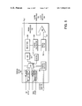
- FIG. 5 illustrates a signal processor 510 including components for monitoring the linefeed drive components Q 1 –Q 6 .
- Analog-to-digital converter (ADC) 520 generates digital values corresponding to the sensed tip and ring node voltages provided by tip/ring sense circuitry 592 .
- the tip/ring sense circuitry provides TIP 1 , TIP 1 –TIP 2 , RING 1 , and RING 1 –RING 2 to ADC 520 .
- TIP 1 is coupled to node 332 and internally to TIP 1 –TIP 2
- node 334 is coupled to TIP 1 –TIP 2
- RING 1 is coupled to node 336 and internally to RING 1 –RING 2
- node 338 is coupled to RING 1 –RING 2 .
- the differential signals can easily be determined through the use of a differential amplifier.
- the differential signals are proportional to the tip and ring line currents. These values are particularly useful for analog control of the subscriber loop.
- the differences are calculated by the power calculator 540 when determining instantaneous power dissipation (as illustrated in FIG. 7 ).
- the linefeed control outputs I 1 –I 4 are provided by control outputs 580 . These currents are also sampled by ADC 520 .
- V BAT is also sampled by ADC 520 .
- V BAT may be assumed to have a pre-determined value.
- the digital representation of sampled values corresponding to TIP 1 , TIP 1 –TIP 2 , RING 1 , RING 1 –RING 2 , I 1 , I 2 , I 3 , I 4 , and V BAT are stored in storage registers 530 .
- instantaneous power dissipation for Q 1 –Q 6 is calculated as V CE ⁇ I C .
- the values stored in registers 530 can then be used by power calculator 540 to determine instantaneous power dissipation for each of Q 1 –Q 6 .
- power calculator 540 includes a multiplier.
- V CQl , V CQ2 The collector voltages (i.e., V CQl , V CQ2 ) are known because the voltage at node 362 (i.e., V 362 ) can readily be determined by the tip sense circuitry.
- V CQ3 and V CQ5 are known because the voltage at node 366 can readily be determined by the ring sense circuitry.
- V BE for each of transistors Q 1 –Q 6 is approximately 0.7 V or ⁇ 0.7 V depending upon transistor type.
- V BAT is either sensed or pre-determined.
- V CE can readily be calculated from the known collector voltage (V CQ1 ) and base-emitter junction voltage.
- the instantaneous power dissipation (p Ql ) can be calculated from V CEQ1 and I 1 .
- V CEQ3 can readily be calculated from the known collector voltage (V CQ3 ) and base-emitter junction voltage.
- Q 3 instantaneous power dissipation can then be calculated from I 3 and V CE of Q 3 .
- the V BE for Q 5 and Q 6 is approximately 0.7 V.
- the voltage drop across resistors R 1 and R 2 is also 0.7 V.
- This information in conjunction with the value of V BAT enables determination of the collector voltages V CQ2 and V CQ4 .
- V CQ2 and V CQ4 Given the base of transistors Q 2 and Q 4 are coupled to signal ground, V CQ2 and V CQ4 also represent the collector-to-base junction voltages for their respective transistors.
- the V BE for these transistors is approximately ⁇ 0.7 V, thus enabling a determination of V CE for transistors Q 2 and Q 4 .
- the voltages at nodes 360 , 362 , 364 , and 366 are known as a result of sampling at nodes 332 , 334 , 336 , and 338 .
- the tip current through RT i.e., I RT .
- I RT V 360 - V 362 RT .
- the base currents of Q 1 –Q 4 are negligible during normal operation of Q 1 –Q 4 such that the collector current (IC) is approximated as the emitter current (I E ) for purposes of estimating power dissipation.
- I CQ1 ⁇ I EQ1 I 1 .
- the collector current for Q 6 can then be determined from I 1 and the tip current I RT .
- V CEQ6 is known from the voltage sampled at node 362 and V BAT .
- the ring current through RR (i.e., I RR ) is determined as
- V CEQ5 is known from the voltage sampled at node 366 and V BAT .
- the collector current for Q 5 is determined from I 3 and the ring current I RR .
- the calculated instantaneous power value for the selected component is then filtered by a digital filter 550 to provide an estimated transistor junction temperature signal 552 .
- filter 550 includes a re-writable nonvolatile memory to permit programming the filter with filter parameters specific to the thermal characteristics of different linefeed transistors. Thus filter 550 can be programmed to handle transistors with different thermal characteristics as the need arises.
- the filter 550 is a low pass filter. Comparator 560 provides a thermal alarm indicator 564 , if the estimated junction temperature signal 552 exceeds a pre-determined junction temperature corresponding to alarm threshold 562 .
- the monitoring function implemented within the signal processor 510 can be achieved using low voltage, fineline, low cost circuitry.
- the monitoring is performed on a time-shared basis such that only one ADC 520 , power calculator 540 , and digital filter 550 are needed to monitor all the linefeed driver transistors as illustrated in FIG. 5 .
- This can be accomplished, for example, through the use of multiplexer 570 with a time-based multiplexer control 572 . This significantly reduces the die size that would otherwise be needed for dedicated, continuous, non-clocked monitoring of each linefeed transistor or each node 360 – 364 .
- ADC 520 may be implemented as a low speed ADC given that thermal events tend to occur slowly.
- ADC 520 is a six bit converter with a sampling rate of a few hundred Hertz.
- FIG. 6 illustrates a method of applying the monitoring function to a selected transistor.
- step 610 the line voltage and line current associated with a selected transistor are determined.
- the instantaneous power dissipation is calculated in step 620 .
- step 630 the instantaneous power is filtered to generate an estimated junction temperature for the selected linefeed transistor.
- the filter is pre-programmed with the appropriate filter parameters corresponding to thermal characteristics particular to the linefeed components.
- Step 640 determines whether the estimated junction temperature exceeds a pre-determined threshold value. If so, then a thermal alarm is provided in step 650 . Otherwise the method is completed in step 690 .
- Another advantage of implementing the monitoring function in the low voltage device as indicated in FIG. 5 is that the digital representation of the line voltages and line currents stored in registers 530 are available for more sophisticated diagnosis of the type of fault condition. These values are also useful for detecting events such as parallel offhook terminal devices as well as for testing the board level of the integrity of the signal processor, the discrete components of the linefeed driver circuitry, and board routing. Yet another advantage is that the digital filter time constant and alarm threshold can be fully programmable.
- Subscriber loop interface circuitry is typically used in conjunction with fuses and overvoltage protection in order to ensure that voltages impressed upon the tip and ring lines do not destroy or otherwise create an electrical or fire hazard for the subscriber loop interface circuitry.
- overvoltage conditions such as a power cross condition
- signals as large as 600 V with high current sourcing capability may exist on tip and ring.
- Protective devices such as fuses are designed to “blow open” in order to avoid damage to the subscriber loop interface circuit 770 and to reduce the risk of fire. All circuitry that cannot withstand 600 V must reside behind the protective fuses.
- One method of verifying the fuse status entails attaching an external load and monitoring the current while driving a voltage signal on the line to determine if the fuse is installed.
- additional dedicated leads may be used for the sole purpose of measuring the unprotected tip and ring signals.
- the first solution involves additional manual steps.
- the second method tends to undesirably increase the number of pins required to implement such functionality on the signal processor.
- External discrete components e.g., resistors
- This attenuation protects the signal processor from large voltages on the line.
- the attenuation protects the signal processor from voltage conditions that a high voltage integrated circuit driving the line directly would not be able to tolerate.
- This enables placement of at least a portion of each of the tip and ring sense circuits on the unprotected side of any tip and ring line fuses.
- the low voltage signal processor is able to diagnose other conditions such as whether a fuse is blown without the need for any additional pins.
- FIG. 7 illustrates subscriber loop interface circuitry including protective devices such as fuses 782 , 792 and overvoltage protection 730 .
- protective devices such as fuses 782 , 792 and overvoltage protection 730 .
- overvoltage conditions such as a power cross condition
- signals as large as 600 V with high current sourcing capability may exist on TIP 780 and RING 790 .
- Protective devices such as fuses 782 and 792 are designed to “blow open” in order to avoid damage to the subscriber loop interface circuit 770 and to reduce the risk of fire. All circuitry that cannot withstand 600 V must reside behind the protective fuses 782 and 792 .
- Signal processor 710 includes TIP/RING sense circuitry 770 with dedicated sense circuitry for each sensed node.
- One embodiment of the sense circuitry 772 is illustrated for TIP 1 .
- a 400 K ⁇ sense resistor (i.e., RS 1 ) exposed to a 600 V tip voltage would generate a sense current, I SENSE of 1.5 mA.
- I SENSE sense current
- Such a current level is well within the tolerance of the low voltage integrated circuit signal processor 710 .
- a typical high voltage integrated circuit has a maximum voltage rating less than 150 V. Thus a high voltage integrated circuit driving the lines directly would be destroyed in the event of a 600 V tip voltage.
- the low voltage signal processor can sense the tip and ring lines across the series-coupled inline components including the typical protection resistors or fuses 782 and 792 such that for a pair of sense lines, one of the pair is not protected by the fuse and the other is electrically protected by the fuse.
- the tip sense lines can be moved across to the unprotected side of fuse 782 at node 760 as indicated by the dotted line at node 763 .
- one of the ring sense lines can be moved to the unprotected side of fuse 792 at node 764 as indicated by the dotted line at node 765 .
- tip sensing can be accomplished across series-coupled tip fuse 782 and tip resistor RT.
- ring sensing can be accomplished across series-coupled ring fuse 792 and ring resistor RR.
- tip and ring sense can be combined with the monitoring of the line before the fuses to enable determining the status of the line or fuses without any additional pins for signal processor 710 . If one of the tip sense leads ( 732 ) is coupled to TIP 780 at node 760 in front of fuse 782 , the tip line voltage can be directly monitored. Similarly if one of the ring sense leads ( 736 ) is coupled to RING 790 at node 764 in front of fuse 792 , the ring line voltage can be directly monitored.
- the line voltage can be directly monitored in a no-load condition to determine if the fuses 782 and 792 have been properly installed.
- the line voltages can still be directly monitored to determine if the power cross condition still exists or if it has been removed, thus providing additional diagnostic capabilities over current solutions.
- this avoids the introduction of extra pins or pins dedicated to monitoring line conditions on the unprotected side of the fuses. This effectively eliminates two pins from the signal processor integrated circuit package such that only four pins are needed to accomplish tip sensing, ring sensing, and direct line monitoring.
- the signal processor integrated circuit package has a first pair of pins for sensing a tip line voltage and a second pair of pins for sensing a ring line voltage, wherein at least one of the first pair of pins is coupled to an unprotected side of a tip fuse, wherein at least one of the second pair of pins is coupled to an unprotected side of a ring fuse.
- Two of the pins sense line conditions before the fuses such that no more than four pins are needed for determining tip and ring line conditions before and after the fuses as well as calculating line voltages and line currents of the linefeed component.
Abstract
Description
p Q1 =I1·(+0.7−V362)
p Q3 =I3·(+0.7−V366)
p Q2 =I 2·(−VBAT+0.7+−0.7V)=−I2·VBAT
p Q4 =I 4·(−VBAT+0.7+−0.7V)=−I4·VBAT
The base currents of Q1–Q4 are negligible during normal operation of Q1–Q4 such that the collector current (IC) is approximated as the emitter current (IE) for purposes of estimating power dissipation. Thus, for example, ICQ1≈IEQ1=I1. The collector current for Q6 can then be determined from I1 and the tip current IRT. VCEQ6 is known from the voltage sampled at
p Q6=(V362−VBAT)·(I1+IRT)
VCEQ5 is known from the voltage sampled at
p Q5=(V366−VBAT)·(I3+I RR)
Claims (16)
Priority Applications (1)
| Application Number | Priority Date | Filing Date | Title |
|---|---|---|---|
| US09/441,380 US7158633B1 (en) | 1999-11-16 | 1999-11-16 | Method and apparatus for monitoring subscriber loop interface circuitry power dissipation |
Applications Claiming Priority (1)
| Application Number | Priority Date | Filing Date | Title |
|---|---|---|---|
| US09/441,380 US7158633B1 (en) | 1999-11-16 | 1999-11-16 | Method and apparatus for monitoring subscriber loop interface circuitry power dissipation |
Publications (1)
| Publication Number | Publication Date |
|---|---|
| US7158633B1 true US7158633B1 (en) | 2007-01-02 |
Family
ID=37592357
Family Applications (1)
| Application Number | Title | Priority Date | Filing Date |
|---|---|---|---|
| US09/441,380 Expired - Fee Related US7158633B1 (en) | 1999-11-16 | 1999-11-16 | Method and apparatus for monitoring subscriber loop interface circuitry power dissipation |
Country Status (1)
| Country | Link |
|---|---|
| US (1) | US7158633B1 (en) |
Cited By (36)
| Publication number | Priority date | Publication date | Assignee | Title |
|---|---|---|---|---|
| US20080224631A1 (en) * | 2007-03-12 | 2008-09-18 | Melanson John L | Color variations in a dimmable lighting device with stable color temperature light sources |
| US20080224636A1 (en) * | 2007-03-12 | 2008-09-18 | Melanson John L | Power control system for current regulated light sources |
| US20080240789A1 (en) * | 2007-03-28 | 2008-10-02 | Fuji Xerox Co., Ltd. | Rotator for powder conveyance and toner cartridge |
| US20080272756A1 (en) * | 2007-05-02 | 2008-11-06 | Melanson John L | Power factor correction controller with digital fir filter output voltage sampling |
| US20090085625A1 (en) * | 2007-09-28 | 2009-04-02 | Melanson John L | Time-based control of a system having integration response |
| US20090147545A1 (en) * | 2007-12-11 | 2009-06-11 | Melanson John L | History-independent noise-immune modulated transformer-coupled gate control signaling method and apparatus |
| US20090190384A1 (en) * | 2008-01-30 | 2009-07-30 | Cirrus Logic, Inc. | Powering a power supply integrated circuit with sense current |
| US20090191837A1 (en) * | 2008-01-30 | 2009-07-30 | Kartik Nanda | Delta Sigma Modulator with Unavailable Output Values |
| US20090189579A1 (en) * | 2008-01-30 | 2009-07-30 | Melanson John L | Switch state controller with a sense current generated operating voltage |
| US20090190379A1 (en) * | 2008-01-30 | 2009-07-30 | John L Melanson | Switching regulator with boosted auxiliary winding supply |
| US20090322300A1 (en) * | 2008-06-25 | 2009-12-31 | Melanson John L | Hysteretic buck converter having dynamic thresholds |
| US20100020570A1 (en) * | 2008-07-25 | 2010-01-28 | Melanson John L | Resonant switching power converter with burst mode transition shaping |
| US20100079125A1 (en) * | 2008-07-25 | 2010-04-01 | Melanson John L | Current sensing in a switching power converter |
| US20100079124A1 (en) * | 2008-09-30 | 2010-04-01 | John Laurence Melanson | Adjustable Constant Current Source with Continuous Conduction Mode ("CCM") and Discontinuous Conduction Mode ("DCM") Operation |
| US20100086121A1 (en) * | 2007-06-16 | 2010-04-08 | Nuvoton Technology Corporation | Method and system for subscriber line interface circuit having a high-voltage mos linefeed circuit |
| US20100148677A1 (en) * | 2008-12-12 | 2010-06-17 | Melanson John L | Time division light output sensing and brightness adjustment for different spectra of light emitting diodes |
| US20100164406A1 (en) * | 2008-07-25 | 2010-07-01 | Kost Michael A | Switching power converter control with triac-based leading edge dimmer compatibility |
| US20100164631A1 (en) * | 2008-12-31 | 2010-07-01 | Cirrus Logic, Inc. | Electronic system having common mode voltage range enhancement |
| US7759881B1 (en) | 2008-03-31 | 2010-07-20 | Cirrus Logic, Inc. | LED lighting system with a multiple mode current control dimming strategy |
| US20100277072A1 (en) * | 2009-04-30 | 2010-11-04 | Draper William A | Calibration Of Lamps |
| US20100328976A1 (en) * | 2009-06-30 | 2010-12-30 | Melanson John L | Cascode configured switching using at least one low breakdown voltage internal, integrated circuit switch to control at least one high breakdown voltage external switch |
| US20100327838A1 (en) * | 2009-06-30 | 2010-12-30 | Melanson John L | Switching power converter with current sensing transformer auxiliary power supply |
| EP2282505A1 (en) * | 2009-08-07 | 2011-02-09 | Zarlink Semiconductor (U.S.) Inc. | Method and apparatus for detecting ring trip precursors |
| US20110074302A1 (en) * | 2009-09-30 | 2011-03-31 | Draper William A | Phase Control Dimming Compatible Lighting Systems |
| US20110110000A1 (en) * | 2009-11-09 | 2011-05-12 | Etter Brett E | Power System Having Voltage-Based Monitoring for Over Current Protection |
| US8018171B1 (en) | 2007-03-12 | 2011-09-13 | Cirrus Logic, Inc. | Multi-function duty cycle modifier |
| US8076920B1 (en) | 2007-03-12 | 2011-12-13 | Cirrus Logic, Inc. | Switching power converter and control system |
| US8102127B2 (en) | 2007-06-24 | 2012-01-24 | Cirrus Logic, Inc. | Hybrid gas discharge lamp-LED lighting system |
| US8150026B2 (en) | 2007-06-16 | 2012-04-03 | Winbond Electronics Corporation | Method and system for subscriber line interface circuit |
| US8212493B2 (en) | 2009-06-30 | 2012-07-03 | Cirrus Logic, Inc. | Low energy transfer mode for auxiliary power supply operation in a cascaded switching power converter |
| US8222872B1 (en) | 2008-09-30 | 2012-07-17 | Cirrus Logic, Inc. | Switching power converter with selectable mode auxiliary power supply |
| US8288954B2 (en) | 2008-12-07 | 2012-10-16 | Cirrus Logic, Inc. | Primary-side based control of secondary-side current for a transformer |
| US8362707B2 (en) | 2008-12-12 | 2013-01-29 | Cirrus Logic, Inc. | Light emitting diode based lighting system with time division ambient light feedback response |
| US8487546B2 (en) | 2008-08-29 | 2013-07-16 | Cirrus Logic, Inc. | LED lighting system with accurate current control |
| US8536794B2 (en) | 2007-03-12 | 2013-09-17 | Cirrus Logic, Inc. | Lighting system with lighting dimmer output mapping |
| US8963535B1 (en) | 2009-06-30 | 2015-02-24 | Cirrus Logic, Inc. | Switch controlled current sensing using a hall effect sensor |
Citations (22)
| Publication number | Priority date | Publication date | Assignee | Title |
|---|---|---|---|---|
| GB2032730A (en) | 1978-08-11 | 1980-05-08 | Hitachi Ltd | Signal processing apparatus for subscriber circuits |
| US4317963A (en) * | 1980-09-22 | 1982-03-02 | International Telephone And Telegraph Corporation | Subscriber line interface circuit utilizing impedance synthesizer and shared voltage source for loop current regulation control |
| US4355341A (en) * | 1980-06-30 | 1982-10-19 | Rca Corporation | Power protection circuit for transistors |
| US4456991A (en) * | 1981-09-18 | 1984-06-26 | International Telephone And Telegraph Corporation | Telephone line circuit and system |
| US4727450A (en) * | 1985-05-13 | 1988-02-23 | Crouzet | Temperature measuring, protection and safety device, thermal protection device using the temperature measuring device and electronic power controller using the thermal protection device |
| US4827505A (en) | 1985-08-20 | 1989-05-02 | Fujitsu Limited | Subscriber line interface circuit |
| US4856059A (en) * | 1987-11-13 | 1989-08-08 | Itec, Inc. | Semiconductor subscriber line interface circuit with enhanced survivability |
| US4982307A (en) * | 1989-12-04 | 1991-01-01 | Ag Communication Systems Corporation | Thermal protection circuit for an integrated circuit subscriber line interface |
| US5175764A (en) | 1990-10-18 | 1992-12-29 | Ag Communication Systems Corporation | Enhanced high voltage line interface circuit |
| US5347577A (en) | 1991-09-05 | 1994-09-13 | Fujitsu Limited | Battery feed circuit for supplying feed current to telephone set |
| US5392334A (en) | 1993-08-25 | 1995-02-21 | Intel Corporation | Off-hook detection and soft line seizure for telephone line sharing in a computer system |
| US5428682A (en) * | 1993-03-12 | 1995-06-27 | Advanced Micro Devices, Inc. | Subscriber line interface circuit with reduced on-chip power dissipation |
| US5488631A (en) * | 1994-10-31 | 1996-01-30 | Radio Connect Corporation | Wireless direct-sequence spread spectrum TDMA communications system |
| US5596637A (en) * | 1993-04-30 | 1997-01-21 | Sgs-Thomson Microelectronics, S.R.L. | Power dissipation manager circuit for an interface device feeding a subscriber telephone line |
| US5636273A (en) | 1995-06-07 | 1997-06-03 | Advanced Micro Devices Inc | Integrated ring detection circuit and power cross detection circuit with persistence timers |
| US5828748A (en) | 1996-06-27 | 1998-10-27 | Lucent Technologies | Method for customizing operation of a line interface circuit in a telecommunications network |
| US5848149A (en) | 1995-05-26 | 1998-12-08 | Lucent Technologies Inc. | Subscriber line interface and power circuit |
| US5881130A (en) * | 1997-09-15 | 1999-03-09 | Teradyne, Inc. | Fast and noise-insensitive load status detection |
| US5917382A (en) * | 1995-10-31 | 1999-06-29 | Stmicroelectronics, S.R.L. | Sensor of the instant power dissipated in a power transistor |
| US6092927A (en) * | 1994-11-10 | 2000-07-25 | International Rectifier Corp. | Temperature detection of power semiconductors performed by a co-packaged analog integrated circuit |
| US6219417B1 (en) * | 1997-06-06 | 2001-04-17 | Advanced Micro Devices, Inc. | Ring trip detection in a communication system |
| US6489793B2 (en) * | 1996-10-21 | 2002-12-03 | Delta Design, Inc. | Temperature control of electronic devices using power following feedback |
-
1999
- 1999-11-16 US US09/441,380 patent/US7158633B1/en not_active Expired - Fee Related
Patent Citations (22)
| Publication number | Priority date | Publication date | Assignee | Title |
|---|---|---|---|---|
| GB2032730A (en) | 1978-08-11 | 1980-05-08 | Hitachi Ltd | Signal processing apparatus for subscriber circuits |
| US4355341A (en) * | 1980-06-30 | 1982-10-19 | Rca Corporation | Power protection circuit for transistors |
| US4317963A (en) * | 1980-09-22 | 1982-03-02 | International Telephone And Telegraph Corporation | Subscriber line interface circuit utilizing impedance synthesizer and shared voltage source for loop current regulation control |
| US4456991A (en) * | 1981-09-18 | 1984-06-26 | International Telephone And Telegraph Corporation | Telephone line circuit and system |
| US4727450A (en) * | 1985-05-13 | 1988-02-23 | Crouzet | Temperature measuring, protection and safety device, thermal protection device using the temperature measuring device and electronic power controller using the thermal protection device |
| US4827505A (en) | 1985-08-20 | 1989-05-02 | Fujitsu Limited | Subscriber line interface circuit |
| US4856059A (en) * | 1987-11-13 | 1989-08-08 | Itec, Inc. | Semiconductor subscriber line interface circuit with enhanced survivability |
| US4982307A (en) * | 1989-12-04 | 1991-01-01 | Ag Communication Systems Corporation | Thermal protection circuit for an integrated circuit subscriber line interface |
| US5175764A (en) | 1990-10-18 | 1992-12-29 | Ag Communication Systems Corporation | Enhanced high voltage line interface circuit |
| US5347577A (en) | 1991-09-05 | 1994-09-13 | Fujitsu Limited | Battery feed circuit for supplying feed current to telephone set |
| US5428682A (en) * | 1993-03-12 | 1995-06-27 | Advanced Micro Devices, Inc. | Subscriber line interface circuit with reduced on-chip power dissipation |
| US5596637A (en) * | 1993-04-30 | 1997-01-21 | Sgs-Thomson Microelectronics, S.R.L. | Power dissipation manager circuit for an interface device feeding a subscriber telephone line |
| US5392334A (en) | 1993-08-25 | 1995-02-21 | Intel Corporation | Off-hook detection and soft line seizure for telephone line sharing in a computer system |
| US5488631A (en) * | 1994-10-31 | 1996-01-30 | Radio Connect Corporation | Wireless direct-sequence spread spectrum TDMA communications system |
| US6092927A (en) * | 1994-11-10 | 2000-07-25 | International Rectifier Corp. | Temperature detection of power semiconductors performed by a co-packaged analog integrated circuit |
| US5848149A (en) | 1995-05-26 | 1998-12-08 | Lucent Technologies Inc. | Subscriber line interface and power circuit |
| US5636273A (en) | 1995-06-07 | 1997-06-03 | Advanced Micro Devices Inc | Integrated ring detection circuit and power cross detection circuit with persistence timers |
| US5917382A (en) * | 1995-10-31 | 1999-06-29 | Stmicroelectronics, S.R.L. | Sensor of the instant power dissipated in a power transistor |
| US5828748A (en) | 1996-06-27 | 1998-10-27 | Lucent Technologies | Method for customizing operation of a line interface circuit in a telecommunications network |
| US6489793B2 (en) * | 1996-10-21 | 2002-12-03 | Delta Design, Inc. | Temperature control of electronic devices using power following feedback |
| US6219417B1 (en) * | 1997-06-06 | 2001-04-17 | Advanced Micro Devices, Inc. | Ring trip detection in a communication system |
| US5881130A (en) * | 1997-09-15 | 1999-03-09 | Teradyne, Inc. | Fast and noise-insensitive load status detection |
Non-Patent Citations (12)
Cited By (76)
| Publication number | Priority date | Publication date | Assignee | Title |
|---|---|---|---|---|
| US8076920B1 (en) | 2007-03-12 | 2011-12-13 | Cirrus Logic, Inc. | Switching power converter and control system |
| US7852017B1 (en) | 2007-03-12 | 2010-12-14 | Cirrus Logic, Inc. | Ballast for light emitting diode light sources |
| US8018171B1 (en) | 2007-03-12 | 2011-09-13 | Cirrus Logic, Inc. | Multi-function duty cycle modifier |
| US8174204B2 (en) | 2007-03-12 | 2012-05-08 | Cirrus Logic, Inc. | Lighting system with power factor correction control data determined from a phase modulated signal |
| US20080224631A1 (en) * | 2007-03-12 | 2008-09-18 | Melanson John L | Color variations in a dimmable lighting device with stable color temperature light sources |
| US8536794B2 (en) | 2007-03-12 | 2013-09-17 | Cirrus Logic, Inc. | Lighting system with lighting dimmer output mapping |
| US20080224636A1 (en) * | 2007-03-12 | 2008-09-18 | Melanson John L | Power control system for current regulated light sources |
| US7804256B2 (en) | 2007-03-12 | 2010-09-28 | Cirrus Logic, Inc. | Power control system for current regulated light sources |
| US20080224629A1 (en) * | 2007-03-12 | 2008-09-18 | Melanson John L | Lighting system with power factor correction control data determined from a phase modulated signal |
| US20080240789A1 (en) * | 2007-03-28 | 2008-10-02 | Fuji Xerox Co., Ltd. | Rotator for powder conveyance and toner cartridge |
| US20080272747A1 (en) * | 2007-05-02 | 2008-11-06 | Cirrus Logic, Inc. | Programmable power control system |
| US20080272758A1 (en) * | 2007-05-02 | 2008-11-06 | Melanson John L | Switching Power Converter with Switch Control Pulse Width Variability at Low Power Demand Levels |
| US7969125B2 (en) | 2007-05-02 | 2011-06-28 | Cirrus Logic, Inc. | Programmable power control system |
| US8040703B2 (en) | 2007-05-02 | 2011-10-18 | Cirrus Logic, Inc. | Power factor correction controller with feedback reduction |
| US7888922B2 (en) | 2007-05-02 | 2011-02-15 | Cirrus Logic, Inc. | Power factor correction controller with switch node feedback |
| US8125805B1 (en) | 2007-05-02 | 2012-02-28 | Cirrus Logic Inc. | Switch-mode converter operating in a hybrid discontinuous conduction mode (DCM)/continuous conduction mode (CCM) that uses double or more pulses in a switching period |
| US7863828B2 (en) | 2007-05-02 | 2011-01-04 | Cirrus Logic, Inc. | Power supply DC voltage offset detector |
| US8120341B2 (en) | 2007-05-02 | 2012-02-21 | Cirrus Logic, Inc. | Switching power converter with switch control pulse width variability at low power demand levels |
| US20080272746A1 (en) * | 2007-05-02 | 2008-11-06 | Cirrus Logic, Inc. | Power factor correction controller with switch node feedback |
| US20080272756A1 (en) * | 2007-05-02 | 2008-11-06 | Melanson John L | Power factor correction controller with digital fir filter output voltage sampling |
| US7821237B2 (en) | 2007-05-02 | 2010-10-26 | Cirrus Logic, Inc. | Power factor correction (PFC) controller and method using a finite state machine to adjust the duty cycle of a PWM control signal |
| US20080273356A1 (en) * | 2007-05-02 | 2008-11-06 | Melanson John L | Switching Power Converter with Efficient Switching Control Signal Period Generation |
| US7894216B2 (en) | 2007-05-02 | 2011-02-22 | Cirrus Logic, Inc. | Switching power converter with efficient switching control signal period generation |
| US8335310B2 (en) | 2007-06-16 | 2012-12-18 | Nuvoton Technology Corporation | Method and system for subscriber line interface circuit having a high-voltage MOS linefeed circuit |
| US8150026B2 (en) | 2007-06-16 | 2012-04-03 | Winbond Electronics Corporation | Method and system for subscriber line interface circuit |
| US20100086121A1 (en) * | 2007-06-16 | 2010-04-08 | Nuvoton Technology Corporation | Method and system for subscriber line interface circuit having a high-voltage mos linefeed circuit |
| US8102127B2 (en) | 2007-06-24 | 2012-01-24 | Cirrus Logic, Inc. | Hybrid gas discharge lamp-LED lighting system |
| US7647125B2 (en) * | 2007-09-28 | 2010-01-12 | Cirrus Logic, Inc. | Time-based control of a system having integration response |
| CN101398670B (en) * | 2007-09-28 | 2012-02-22 | 塞瑞斯逻辑公司 | Time-based control of a system having integration response and control method |
| US20090085625A1 (en) * | 2007-09-28 | 2009-04-02 | Melanson John L | Time-based control of a system having integration response |
| US7804697B2 (en) | 2007-12-11 | 2010-09-28 | Cirrus Logic, Inc. | History-independent noise-immune modulated transformer-coupled gate control signaling method and apparatus |
| US20090147545A1 (en) * | 2007-12-11 | 2009-06-11 | Melanson John L | History-independent noise-immune modulated transformer-coupled gate control signaling method and apparatus |
| US8576589B2 (en) | 2008-01-30 | 2013-11-05 | Cirrus Logic, Inc. | Switch state controller with a sense current generated operating voltage |
| US8008898B2 (en) | 2008-01-30 | 2011-08-30 | Cirrus Logic, Inc. | Switching regulator with boosted auxiliary winding supply |
| US20090190379A1 (en) * | 2008-01-30 | 2009-07-30 | John L Melanson | Switching regulator with boosted auxiliary winding supply |
| US20090189579A1 (en) * | 2008-01-30 | 2009-07-30 | Melanson John L | Switch state controller with a sense current generated operating voltage |
| US20090191837A1 (en) * | 2008-01-30 | 2009-07-30 | Kartik Nanda | Delta Sigma Modulator with Unavailable Output Values |
| US20090190384A1 (en) * | 2008-01-30 | 2009-07-30 | Cirrus Logic, Inc. | Powering a power supply integrated circuit with sense current |
| US8022683B2 (en) | 2008-01-30 | 2011-09-20 | Cirrus Logic, Inc. | Powering a power supply integrated circuit with sense current |
| US7755525B2 (en) | 2008-01-30 | 2010-07-13 | Cirrus Logic, Inc. | Delta sigma modulator with unavailable output values |
| US7759881B1 (en) | 2008-03-31 | 2010-07-20 | Cirrus Logic, Inc. | LED lighting system with a multiple mode current control dimming strategy |
| US20090322300A1 (en) * | 2008-06-25 | 2009-12-31 | Melanson John L | Hysteretic buck converter having dynamic thresholds |
| US8008902B2 (en) | 2008-06-25 | 2011-08-30 | Cirrus Logic, Inc. | Hysteretic buck converter having dynamic thresholds |
| US20100020573A1 (en) * | 2008-07-25 | 2010-01-28 | Melanson John L | Audible noise suppression in a resonant switching power converter |
| US20100079125A1 (en) * | 2008-07-25 | 2010-04-01 | Melanson John L | Current sensing in a switching power converter |
| US8014176B2 (en) | 2008-07-25 | 2011-09-06 | Cirrus Logic, Inc. | Resonant switching power converter with burst mode transition shaping |
| US20100020570A1 (en) * | 2008-07-25 | 2010-01-28 | Melanson John L | Resonant switching power converter with burst mode transition shaping |
| US8553430B2 (en) | 2008-07-25 | 2013-10-08 | Cirrus Logic, Inc. | Resonant switching power converter with adaptive dead time control |
| US20100020569A1 (en) * | 2008-07-25 | 2010-01-28 | Melanson John L | Resonant switching power converter with adaptive dead time control |
| US8212491B2 (en) | 2008-07-25 | 2012-07-03 | Cirrus Logic, Inc. | Switching power converter control with triac-based leading edge dimmer compatibility |
| US20100164406A1 (en) * | 2008-07-25 | 2010-07-01 | Kost Michael A | Switching power converter control with triac-based leading edge dimmer compatibility |
| US8344707B2 (en) | 2008-07-25 | 2013-01-01 | Cirrus Logic, Inc. | Current sensing in a switching power converter |
| US8279628B2 (en) | 2008-07-25 | 2012-10-02 | Cirrus Logic, Inc. | Audible noise suppression in a resonant switching power converter |
| US8487546B2 (en) | 2008-08-29 | 2013-07-16 | Cirrus Logic, Inc. | LED lighting system with accurate current control |
| US20100079124A1 (en) * | 2008-09-30 | 2010-04-01 | John Laurence Melanson | Adjustable Constant Current Source with Continuous Conduction Mode ("CCM") and Discontinuous Conduction Mode ("DCM") Operation |
| US8179110B2 (en) | 2008-09-30 | 2012-05-15 | Cirrus Logic Inc. | Adjustable constant current source with continuous conduction mode (“CCM”) and discontinuous conduction mode (“DCM”) operation |
| US8222872B1 (en) | 2008-09-30 | 2012-07-17 | Cirrus Logic, Inc. | Switching power converter with selectable mode auxiliary power supply |
| US8288954B2 (en) | 2008-12-07 | 2012-10-16 | Cirrus Logic, Inc. | Primary-side based control of secondary-side current for a transformer |
| US8362707B2 (en) | 2008-12-12 | 2013-01-29 | Cirrus Logic, Inc. | Light emitting diode based lighting system with time division ambient light feedback response |
| US20100148677A1 (en) * | 2008-12-12 | 2010-06-17 | Melanson John L | Time division light output sensing and brightness adjustment for different spectra of light emitting diodes |
| US8299722B2 (en) | 2008-12-12 | 2012-10-30 | Cirrus Logic, Inc. | Time division light output sensing and brightness adjustment for different spectra of light emitting diodes |
| US20100164631A1 (en) * | 2008-12-31 | 2010-07-01 | Cirrus Logic, Inc. | Electronic system having common mode voltage range enhancement |
| US7994863B2 (en) | 2008-12-31 | 2011-08-09 | Cirrus Logic, Inc. | Electronic system having common mode voltage range enhancement |
| US8482223B2 (en) | 2009-04-30 | 2013-07-09 | Cirrus Logic, Inc. | Calibration of lamps |
| US20100277072A1 (en) * | 2009-04-30 | 2010-11-04 | Draper William A | Calibration Of Lamps |
| US8198874B2 (en) | 2009-06-30 | 2012-06-12 | Cirrus Logic, Inc. | Switching power converter with current sensing transformer auxiliary power supply |
| US8212493B2 (en) | 2009-06-30 | 2012-07-03 | Cirrus Logic, Inc. | Low energy transfer mode for auxiliary power supply operation in a cascaded switching power converter |
| US20100328976A1 (en) * | 2009-06-30 | 2010-12-30 | Melanson John L | Cascode configured switching using at least one low breakdown voltage internal, integrated circuit switch to control at least one high breakdown voltage external switch |
| US8248145B2 (en) | 2009-06-30 | 2012-08-21 | Cirrus Logic, Inc. | Cascode configured switching using at least one low breakdown voltage internal, integrated circuit switch to control at least one high breakdown voltage external switch |
| US20100327838A1 (en) * | 2009-06-30 | 2010-12-30 | Melanson John L | Switching power converter with current sensing transformer auxiliary power supply |
| US8963535B1 (en) | 2009-06-30 | 2015-02-24 | Cirrus Logic, Inc. | Switch controlled current sensing using a hall effect sensor |
| EP2282505A1 (en) * | 2009-08-07 | 2011-02-09 | Zarlink Semiconductor (U.S.) Inc. | Method and apparatus for detecting ring trip precursors |
| US20110074302A1 (en) * | 2009-09-30 | 2011-03-31 | Draper William A | Phase Control Dimming Compatible Lighting Systems |
| US9155174B2 (en) | 2009-09-30 | 2015-10-06 | Cirrus Logic, Inc. | Phase control dimming compatible lighting systems |
| US20110110000A1 (en) * | 2009-11-09 | 2011-05-12 | Etter Brett E | Power System Having Voltage-Based Monitoring for Over Current Protection |
| US8654483B2 (en) | 2009-11-09 | 2014-02-18 | Cirrus Logic, Inc. | Power system having voltage-based monitoring for over current protection |
Similar Documents
| Publication | Publication Date | Title |
|---|---|---|
| US7158633B1 (en) | Method and apparatus for monitoring subscriber loop interface circuitry power dissipation | |
| US6058161A (en) | System and method for programmable telephone subscriber line test | |
| US5175764A (en) | Enhanced high voltage line interface circuit | |
| US6144722A (en) | System and method for programmable telephone subscriber line test in ring mode | |
| US20070201686A1 (en) | Subscriber Line Interface Circuitry | |
| US5956386A (en) | Telephone subscriber line diagnostics system and method | |
| US6169785B1 (en) | Apparatus and method for testing subscriber line | |
| JP4044962B2 (en) | Telephone line monitor circuit | |
| US4551671A (en) | Terminal disconnect and media wire fault detect mechanism | |
| US4373121A (en) | Maintenance termination device | |
| US6301227B1 (en) | Systems and methods for allowing transmission systems to effectively respond to automated test procedures | |
| US20100124326A1 (en) | Subscriber line interface circuitry with common base audio isolation stage | |
| US5345496A (en) | Remote line test facility | |
| US4262172A (en) | Ring-trip detector | |
| US7254230B2 (en) | Subscriber line interface circuitry | |
| US20020089804A1 (en) | Circuit topology for protecting vulnerable micro electro-mechanical system (MEMS) and electronic relay devices | |
| US4492821A (en) | Subscriber connection circuit | |
| US4149040A (en) | Identifier circuit for identifying party line subscribers | |
| US6567520B1 (en) | Method and apparatus for detecting multiple telephone off-hook conditions | |
| US8102970B2 (en) | Method and apparatus for line testing | |
| WO2004077801A1 (en) | Device and method for detecting presence of service on telephone line | |
| US8948347B2 (en) | Method and device for checking the connection of a positive supply voltage to a subscriber access line comprising a plurality of wires | |
| EP1031230B1 (en) | Method and apparatus for testing a subscriber line interface | |
| JP3414619B2 (en) | Subscriber line measurement method and device | |
| JPS62233968A (en) | Current supply circuit |
Legal Events
| Date | Code | Title | Description |
|---|---|---|---|
| AS | Assignment |
Owner name: SILICON LABORATORIES, INC., TEXAS Free format text: ASSIGNMENT OF ASSIGNORS INTEREST;ASSIGNOR:HEIN, JERRELL P.;REEL/FRAME:010405/0953 Effective date: 19991101 |
|
| FEPP | Fee payment procedure |
Free format text: PAYOR NUMBER ASSIGNED (ORIGINAL EVENT CODE: ASPN); ENTITY STATUS OF PATENT OWNER: LARGE ENTITY |
|
| FPAY | Fee payment |
Year of fee payment: 4 |
|
| FPAY | Fee payment |
Year of fee payment: 8 |
|
| FEPP | Fee payment procedure |
Free format text: MAINTENANCE FEE REMINDER MAILED (ORIGINAL EVENT CODE: REM.) |
|
| LAPS | Lapse for failure to pay maintenance fees |
Free format text: PATENT EXPIRED FOR FAILURE TO PAY MAINTENANCE FEES (ORIGINAL EVENT CODE: EXP.); ENTITY STATUS OF PATENT OWNER: LARGE ENTITY |
|
| STCH | Information on status: patent discontinuation |
Free format text: PATENT EXPIRED DUE TO NONPAYMENT OF MAINTENANCE FEES UNDER 37 CFR 1.362 |
|
| FP | Lapsed due to failure to pay maintenance fee |
Effective date: 20190102 |