US7149947B1 - Method of and system for validating an error correction code and parity information associated with a data word - Google Patents
Method of and system for validating an error correction code and parity information associated with a data word Download PDFInfo
- Publication number
- US7149947B1 US7149947B1 US10/654,852 US65485203A US7149947B1 US 7149947 B1 US7149947 B1 US 7149947B1 US 65485203 A US65485203 A US 65485203A US 7149947 B1 US7149947 B1 US 7149947B1
- Authority
- US
- United States
- Prior art keywords
- bits
- digital word
- error correction
- correction code
- data
- Prior art date
- Legal status (The legal status is an assumption and is not a legal conclusion. Google has not performed a legal analysis and makes no representation as to the accuracy of the status listed.)
- Active, expires
Links
Images


Classifications
-
- G—PHYSICS
- G06—COMPUTING; CALCULATING OR COUNTING
- G06F—ELECTRIC DIGITAL DATA PROCESSING
- G06F11/00—Error detection; Error correction; Monitoring
- G06F11/07—Responding to the occurrence of a fault, e.g. fault tolerance
- G06F11/08—Error detection or correction by redundancy in data representation, e.g. by using checking codes
- G06F11/10—Adding special bits or symbols to the coded information, e.g. parity check, casting out 9's or 11's
- G06F11/1008—Adding special bits or symbols to the coded information, e.g. parity check, casting out 9's or 11's in individual solid state devices
Definitions
- This invention relates generally to a method of and system for validating error correction code and parity information associated with a data word and more particularly to a method of and system for validating proper generation of error correction codes when the data over which the error correction code is generated is originally protected by simple parity.
- FIG. 1 One example of such a system is shown at 10 in FIG. 1 .
- the data is transmitted from upstream logic 12 to downstream logic 20 .
- the data, along with the associated parity bits, are transmitted to a parity checker 14 which compares the parity of the transmitted data word with the parity bits to determine whether an error has occurred in either the data or the parity bits.
- the data, without the parity bits, is also transmitted to ECC generator 16 , which generates an error correction code in accordance with known algorithms.
- the data with ECC is then transmitted to downstream logic 20 . While this system incorporates both parity and ECC error detection schemes, it is still vulnerable to undetected errors because the data travels in separate paths to the parity checker 14 and the ECC generator 16 .
- the parity checker 14 would indicate correct parity, but the ECC generated by the ECC generator 16 would be based on faulty data and would thus be incorrect.
- a similar error could occur if the data was corrupted in the path to the parity checker 14 , if the corruption resulted in incorrect parity.
- system 30 transmits data from upstream logic 32 to downstream logic 42 and the parity of the data is checked in parity checker 34 .
- the data is passed through two separate ECC generators 36 , 38 and the resulting ECCs are compared to each other in comparator 40 before being passed to the downstream logic 40 .
- This system 30 would be likely to detect any errors that occurred in the data downstream of intersection 44 , since, if the data is corrupted in either of branches 46 and 48 , the resulting ECC codes from ECC generators 36 , 38 would be different and if the data is corrupted in branch 50 , the parity checker 34 will detect a change in parity of the data. However, if the data is corrupted at point 52 , both ECC generators will generate the same, incorrect ECC and, depending on the parity of the incorrect data, the parity checker 34 might not detect the error.
- the present invention provides a method of and system for validating error correction codes that are generated for the purpose of indicating whether errors are present in digital words transmitted throughout a computer system by combining the parity checker and the generation of the ECCs.
- the system generates a first error correction code for a digital word using an error correction code generating scheme such as a modified Hamming code.
- a second error correction code is generated using an inverted version of the error correction code generating scheme used to generate the first error correction code.
- the first and second error correction codes are logically compared to generate a data signature that is then logically compared to the parity information associated with the original digital word. The result of this logical comparison is compared to a predetermined constant to determine whether an error is present in the original data word, in the parity, in the first error correction code or in the second error correction code.
- a method for operating a data processing system includes:
- G determining that an error has occurred in at least one of the N bits of data in the digital word, the M bits of data in the digital word, the first error correction code and the second error correction code if the generated constant signal is different from the predetermined constant signal.
- the first error correction code may include Y bits, wherein each one of the Y bits may be generated by performing a third logic operation on predetermined bit sets of the digital word. At least two of the Y bits of the first error correction code may be generated by performing the third logic operation on different predetermined bit sets of the digital word.
- the second error correction code may include Y bits, wherein each one of the Y bits of the second error correction code may be generated by performing a fourth logic operation on bits of the digital word which are not included in the predetermined bit set of the digital word used to generate a corresponding bit of the first error correction code.
- the M bits of the digital word for error correction may be parity bits.
- the predetermined constant signal may include Z bits, all of which being one of all zeros and all ones.
- the generated constant signal may include Z bits and, if no errors are present in at least one of the N bits of data in the digital word, the M bits of data in the digital word, the first error correction code and the second error correction code, all of the Z bits of the generated constant signal are one of all zeros and all ones.
- the first logic operation and the second logic operation each may be an XOR operation.
- the third logic operation and the fourth logic operation each may be one of an XOR operation and an XNOR operation. If no errors are present in the N bits of the digital word, the second error correction code may be one of identical to the first error correction code and opposite to the first error correction code. If no errors are present in the N bits of the digital word, the digital signature may include one of all zeros and all ones.
- the digital signature may include all zeros. If the N bits of the digital word are odd, and if no errors are present in the N bits of the digital word, the digital signature may include all ones. If the N bits of the digital word are even, and if no errors are present in the N bits of the digital word, the second error correction code may be identical to the first error correction code. If the N bits of the digital word are odd, and if no errors are present in the N bits of the digital word, the second error correction code may be opposite the first error correction code.
- a data processing system includes an input portion for receiving a digital word having N bits of data and M bits for error detection; a first error correction code generator for generating a first error correction code based on the N bits of data of the digital word; a second error correction code generator for generating a second error correction code based on the N bits of data of the digital word; a first logic operator for performing a first logic operation on the first error correction code and the second error correction code to generate a data signature representative of a comparison of the first error correction code and the second error correction code; and a second logic operator for performing a second logic operation on the data signature and the M bits of the digital word to generate a constant signal representing a comparison of the data signature and the M bits of the digital word.
- the system further includes a comparator for comparing the generated constant signal to a predetermined constant signal to determine if an error has occurred in at least one of the N bits of data in the digital word, the M bits of data in the digital word, the first error correction code and the second error correction code; and an error signal generator for generating an error signal indicating that an error has occurred in at least one of the N bits of data in the digital word, the M bits of data in the digital word, the first error correction code and the second error correction code if the generated constant signal is different from the predetermined constant signal.
- a method for operating a data processing system includes:
- the method may further include:
- G comparing the generated constant signal to a predetermined constant signal to determine if an error has occurred in at least one of the N bits of data in the digital word, the M bits of data in the digital word, the primary error correction code and the complementary error correction code;
- a data processing system includes an input portion for receiving a digital word having N bits of data and M bits for error detection; a primary error correction code generator for generating a primary error correction code based on the N bits of data of the digital word; and a complementary error correction code generator for generating a complementary error correction code based on the N bits of data of the digital word.
- the system further includes a first logic operator for performing a first logic operation on the primary error correction code and the complementary error correction code to generate a data signature representative of a comparison of the primary error correction code and the complementary error correction code; and an error detection device which detects whether an error has occurred in at least one of the N bits of the digital word, the primary error correction code and the complementary error correction code based on the value of the data signature.
- the system may further include a second logic operator for performing a second logic operation on the data signature and the M bits of the digital word to generate a constant signal representing a comparison of the data signature and the M bits of the digital word; a comparator for comparing the generated constant signal to a predetermined constant signal to determine if an error has occurred in at least one of the N bits of data in the digital word, the M bits of data in the digital word, the primary error correction code and the complementary error correction code; and an error signal generator for generating an error signal indicating that an error has occurred in at least one of the N bits of data in the digital word, the M bits of data in the digital word, the primary error correction code and the complementary error correction code if the generated constant signal is different from the predetermined constant signal.
- a second logic operator for performing a second logic operation on the data signature and the M bits of the digital word to generate a constant signal representing a comparison of the data signature and the M bits of the digital word
- a comparator for comparing the generated constant signal to a predetermined constant signal to determine
- FIG. 1 is a schematic block diagram of a prior art data error checking system
- FIG. 2 is a schematic block diagram of another prior art data error checking system
- FIG. 3 is a schematic block diagram of an error correction code validation system in accordance with the present invention.
- FIG. 4 is a detailed schematic block diagram of the ECC and parity validation device of FIG. 3 ;
- FIG. 5 is a flow diagram showing the steps performed by the error correction code validation system in accordance with the present invention.
- FIG. 6 is a table showing an example of an error correction code generation scheme.
- a data word with parity information received from the upstream logic 102 is transmitted through registers 104 and 106 before it is input to ECC and parity validation device 108 .
- the data word without parity is also transmitted from the register 106 to the downstream logic 114 .
- the data word without the parity is transmitted from register 104 to the ECC generator 110 , where the ECC for the data word is generated in a manner known in the art.
- the ECC is generated using a modified Hamming generation scheme. It will be understood, however, that any type of ECC generation scheme may be utilized by the ECC generator 110 , such as Reed-Solomon codes, etc.
- the ECC is then transmitted from the ECC generator 110 through a register 112 and to the ECC and parity validation device 108 . As shown in FIG. 3 , the ECC is also transmitted to the downstream logic 114 .
- registers 104 , 106 and 112 are included in the preferred embodiment for the purpose of synchronizing the flow of data through the system 100 , it will be understood that these registers are not essential to the operation of the invention and may be omitted.
- the ECC and parity validation device 108 is shown in greater detail in FIG. 4 .
- the ECC and parity validation device 108 includes a complementary ECC (CECC) generator 120 , which receives the data-only portion of the digital data word from register 106 .
- the CECC generator generates a complementary ECC based on the same ECC generation scheme utilized by the ECC generator 110 to generate the ECC. The details of the operation of the CECC generator 120 are described below with reference to FIGS. 5 and 6 .
- the complementary ECC generated by the complementary ECC generator 120 is input to an XOR operator 122 where an exclusive-or operation is performed on the CECC and the ECC input to the XOR operator from register 112 .
- the result of the XOR operation is the data signature, which typically includes the same number of bits as the ECC and the CECC.
- the data signature is then input to an XOR operator 124 where an exclusive-or operation is performed on the data signature and the parity bit or bits input to the XOR operator from register 104 .
- the result of the XOR operation is a generated constant, which also typically includes the same number of bits as the ECC and the CECC. Finally, the generated constant is compared to a predetermined constant in comparator 126 .
- the predetermined constant is hard-coded in logic (not shown) and typically includes the same number of bits as the generated constant. As described below, the predetermined constant typically includes all 1's or all 0's.
- the comparator 126 performs an exclusive-or operation on the generated constant and the predetermined constant and then performs and OR reduction of the result to produce a single bit error signal output, which typically is a logic 1 if an error is present in either the original data word, the parity, the ECC or the CECC. A logic 0 is output if no error is detected. The error signal is output to the downstream logic 114 .
- FIG. 5 shows a flow diagram 130 of the steps carried out by the ECC and parity validation device 108
- FIG. 6 shows a table 150 of an example of an ECC generation scheme that may be utilized by the ECC generator 110 and the CECC generator 120 .
- Table 150 shows an ECC generation scheme for an 8-bit data word. While data systems which will utilize the device of the present invention typically operate on data words of up to 64-bits or larger, for the sake of simplicity, the invention will be described as it applies to the validation of the ECC and parity associated with an 8-bit data word. Those skilled in the art will understand how to scale the invention to apply to larger data words.
- check bits are labeled (C)ECC 0 –(C)ECC 3 in table 150 .
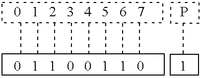
- Each bit in the data word is numbered from 0–7, with the “0” bit being the most significant bit and the “7” bit being the least significant.
- the bits indicated with an “X” in each row associated with a particular check bit are combined using the logic operation shown in the “parity” column. For example, to form check bit ECC 0 , an XOR operation is performed on the bits numbered 0 , 3 , 4 , 6 and 7 of the data word. It will be understood that, in addition to the XOR operation, other logic operations, such as the XNOR operation, for example, may be used to generate each check bit.
- each check bit of the complementary ECC is formed by performing the logic operation indicated in the “parity” column on the bits not included in the ECC generation operation for that check bit. These bits are indicated with an “A” in each row associated with a particular check bit CECC. For example, to form check bit CECC 0 , an XOR operation is performed on the bits numbered 1 , 2 and 5 of the data word.
- Step 132 of FIG. 5 a digital word including a data portion and a parity portion is received in register 104 from upstream logic 102 .
- the data portion of received data word is 01100110 and the parity portion is a single bit 1 , based on an odd parity scheme.
- the data word and, for the purpose of demonstrating the generation of the ECC and CECC bits according to table 150 , an indication of the number 0–7 of each bit and the parity bit P:
- the data portion of the data word is input to ECC generator 110 , which generates the ECC by performing the indicated operation on the indicated bits for each bit of the ECC, Step 134 .
- the operation for each bit ECC 0 to ECC 4 is as follows:
- ECC output from ECC generator 110 is 1110.
- the data with parity is input to the ECC and parity validation device 108 through register 106 , and the data portion is input to complementary ECC (CECC) generator 120 , which generates the CECC by performing the indicated operation on the indicated bits for each bit of the CECC, Step 136 .
- CECC complementary ECC
- the operation for each bit CECC 0 to CECC 3 is as follows:
- CECC output from CECC generator 120 is 1110.
- the ECC and CECC are input to XOR operator 122 which performs an exclusive-or operation on the codes to generate the data signature, Step 138 . Performing an XOR operation on the ECC (1110) and the CECC (1110) yields a data signature of 0000.
- the data signature and the parity portion of the data word are input to XOR operator 124 to generate the generated constant, Step 140 .
- Performing an XOR operation on each bit of the data signature (0000) and the parity portion (1) yields a generated constant of 1111.
- the generated constant is then input to comparator 126 where it is compared to the predetermined constant, Step 142 .
- the comparator 126 comprises an XOR operation and then an OR reduction of the syndrome to produce a 1 bit output.
- the OR reduction of this syndrome yields an output of “0”, indicating that no error has occurred in each of the data word, the parity, the ECC and the CECC, Step 146 . If an error had occurred, as will be shown in an example below, the OR reduction would result in an error output of “1”, indicating that an error had occurred, Step 148 .
- Step 140 determines whether an error has occurred in the parity bit since, in the case of the even data word, each bit of the data signature (0000) is XORed with the parity bit ( 1 ), resulting in a generated constant (1111). In the case of the odd data word, each bit of the data signature (1111) is XORed with the parity bit ( 0 ), also resulting in a generated constant (1111).
- ECC output from ECC generator 110 is 1101.
- CECC output from CECC generator 120 is 0010.
- Performing an XOR operation on the ECC (1101) and the CECC (0010) yields a data signature of 1111.
- Performing an XOR operation on each bit of the data signature (1111) and the parity portion (O) yields a generated constant of 1111.
- the generated constant is then compared to the predetermined constant.
- the comparator 126 comprises an XOR operation and then an OR reduction of the syndrome to produce a 1 bit output.
- the XOR of the generated constant (1111) and our predetermined constant (1111) yields a syndrome 0000, indicating that the generated constant is equal to the predetermined constant.
- the OR reduction of this syndrome yields an output of “0”, indicating that no error has occurred in each of the data word, the parity, the ECC and the CECC.
- bit number 2 has flipped from a 1 to a 0
- the invention operates as follows:
- the ECC generator 110 Since the incorrect data word at B (01000110) is input to the ECC generator 110 , using the generation scheme shown in table 150 of FIG. 6 , the ECC will be 1101. The correct data word at A (01100110) is input to the CECC generator 120 , resulting in a CECC of 1110. The XOR operation in operator 122 yields a data signature of 0011. The XOR operation in operator 124 yields a generated constant of 1100. In comparator 126 , the syndrome of the generated constant (1100) and the predetermined constant (1111) is 0011. The OR reduction of this syndrome yields an error signal of 1, indicating that an error has occurred.
- the output of the CECC generator will be 1110.
- the ECC input is 1100, i.e., the check bit ECC 2 has flipped from a 1 to a 0.
- the data signature output from XOR operator 122 will be 0010.
- the generated constant output from XOR operator 124 will be 1101, which, when compared to the predetermined constant 1111, will result in an error signal 1 output to the downstream logic 114 .
- Example 1 if the parity bit was incorrectly flipped from a 1 to a 0, the generated constant, resulting from the XOR operation performed on the data signature (0000) and the parity bit ( 0 ) in XOR operator 124 , would be 0000, which, when compared to the predetermined constant 1111, would result in a syndrome of 1111.
- the OR reduction would yield an error signal of 1, indicating the error.
- the present invention provides a system and method for validating the ECC and parity information associated with a data word.
- the validation of the ECC and parity information is performed within a single operation, such that an error in the data word, the parity or the ECC is indicated with a single output to the downstream logic.
Abstract
Description

-
- ECC0=0
XOR 0XOR 0XOR 1XOR 0=1 - ECC1=0
XOR 1XOR 0XOR 1XOR 1=1 - ECC2=1
XOR 1XOR 0XOR 1=1 - ECC3=1
XOR 0XOR 1XOR 0=0
- ECC0=0
-
- CECC0=1
XOR 1XOR 1=1 - CECC1=1
XOR 0XOR 0=1 - CECC2=0
XOR 0XOR 1XOR 0=1 - CECC3=0
XOR 1XOR 0XOR 1=0
- CECC0=1

-
- ECC0=0
XOR 0XOR 0XOR 1XOR 0=1 - ECC1=0
XOR 1XOR 0XOR 1XOR 1=1 - ECC2=1
XOR 0XOR 0XOR 1=0 - ECC3=0
XOR 0XOR 1XOR 0=1
- ECC0=0
-
- CECC0=1
XOR 0XOR 1=0 - CECC1=0
XOR 0XOR 0=0 - CECC2=0
XOR 0XOR 1XOR 0=1 - CECC3=0
XOR 1XOR 0XOR 1=0
- CECC0=1

but, through a transmission error, the same data word at point B is:

i.e.,
the output of the CECC generator will be 1110. However, assume an error occurs in the generation of the ECC by the
Claims (54)
Priority Applications (1)
| Application Number | Priority Date | Filing Date | Title |
|---|---|---|---|
| US10/654,852 US7149947B1 (en) | 2003-09-04 | 2003-09-04 | Method of and system for validating an error correction code and parity information associated with a data word |
Applications Claiming Priority (1)
| Application Number | Priority Date | Filing Date | Title |
|---|---|---|---|
| US10/654,852 US7149947B1 (en) | 2003-09-04 | 2003-09-04 | Method of and system for validating an error correction code and parity information associated with a data word |
Publications (1)
| Publication Number | Publication Date |
|---|---|
| US7149947B1 true US7149947B1 (en) | 2006-12-12 |
Family
ID=37497419
Family Applications (1)
| Application Number | Title | Priority Date | Filing Date |
|---|---|---|---|
| US10/654,852 Active 2024-12-10 US7149947B1 (en) | 2003-09-04 | 2003-09-04 | Method of and system for validating an error correction code and parity information associated with a data word |
Country Status (1)
| Country | Link |
|---|---|
| US (1) | US7149947B1 (en) |
Cited By (39)
| Publication number | Priority date | Publication date | Assignee | Title |
|---|---|---|---|---|
| US20050149824A1 (en) * | 2003-12-22 | 2005-07-07 | International Business Machines Corporation | Method for fast ECC memory testing by software including ECC check byte |
| US20070028156A1 (en) * | 2005-07-27 | 2007-02-01 | Carrier Corporation | Method for detecting and correcting operating data errors |
| US20080141043A1 (en) * | 2006-12-06 | 2008-06-12 | David Flynn | Apparatus, system, and method for managing data using a data pipeline |
| US20080155193A1 (en) * | 2006-12-22 | 2008-06-26 | Fujitsu Limited | Staging method for disk array apparatus |
| US20090110109A1 (en) * | 2007-10-29 | 2009-04-30 | Maurizio Skerlj | Apparatus and method for generating a transmit signal and apparatus and method for extracting an original message from a received signal |
| US20090222709A1 (en) * | 2008-02-28 | 2009-09-03 | Ip Video Communications Coporation | Universal packet loss recovery system for delivery of real-time streaming multimedia content over packet-switched networks |
| US20100223527A1 (en) * | 2009-03-02 | 2010-09-02 | Nec Electronics Corporation | Data protection circuit, data protection method, and data processing apparatus |
| US20120233383A1 (en) * | 2011-03-07 | 2012-09-13 | Kabushiki Kaisha Toshiba | Memory system and memory controller |
| US8316277B2 (en) | 2007-12-06 | 2012-11-20 | Fusion-Io, Inc. | Apparatus, system, and method for ensuring data validity in a data storage process |
| US8443134B2 (en) | 2006-12-06 | 2013-05-14 | Fusion-Io, Inc. | Apparatus, system, and method for graceful cache device degradation |
| US8489817B2 (en) | 2007-12-06 | 2013-07-16 | Fusion-Io, Inc. | Apparatus, system, and method for caching data |
| US8706968B2 (en) | 2007-12-06 | 2014-04-22 | Fusion-Io, Inc. | Apparatus, system, and method for redundant write caching |
| US8719501B2 (en) | 2009-09-08 | 2014-05-06 | Fusion-Io | Apparatus, system, and method for caching data on a solid-state storage device |
| US8825937B2 (en) | 2011-02-25 | 2014-09-02 | Fusion-Io, Inc. | Writing cached data forward on read |
| US8874823B2 (en) | 2011-02-15 | 2014-10-28 | Intellectual Property Holdings 2 Llc | Systems and methods for managing data input/output operations |
| US8966184B2 (en) | 2011-01-31 | 2015-02-24 | Intelligent Intellectual Property Holdings 2, LLC. | Apparatus, system, and method for managing eviction of data |
| US9003104B2 (en) | 2011-02-15 | 2015-04-07 | Intelligent Intellectual Property Holdings 2 Llc | Systems and methods for a file-level cache |
| US20150120035A1 (en) * | 2013-10-25 | 2015-04-30 | Infineon Technologies Ag | Systems and Methods for Linking Trace Information with Sensor Data |
| US9058123B2 (en) | 2012-08-31 | 2015-06-16 | Intelligent Intellectual Property Holdings 2 Llc | Systems, methods, and interfaces for adaptive persistence |
| US9104599B2 (en) | 2007-12-06 | 2015-08-11 | Intelligent Intellectual Property Holdings 2 Llc | Apparatus, system, and method for destaging cached data |
| US9116823B2 (en) | 2006-12-06 | 2015-08-25 | Intelligent Intellectual Property Holdings 2 Llc | Systems and methods for adaptive error-correction coding |
| US9116812B2 (en) | 2012-01-27 | 2015-08-25 | Intelligent Intellectual Property Holdings 2 Llc | Systems and methods for a de-duplication cache |
| US9170754B2 (en) | 2007-12-06 | 2015-10-27 | Intelligent Intellectual Property Holdings 2 Llc | Apparatus, system, and method for coordinating storage requests in a multi-processor/multi-thread environment |
| US9201677B2 (en) | 2011-05-23 | 2015-12-01 | Intelligent Intellectual Property Holdings 2 Llc | Managing data input/output operations |
| US20150370677A9 (en) * | 2012-06-04 | 2015-12-24 | Amplidata Nv | Distributed object storage system |
| US9251052B2 (en) | 2012-01-12 | 2016-02-02 | Intelligent Intellectual Property Holdings 2 Llc | Systems and methods for profiling a non-volatile cache having a logical-to-physical translation layer |
| US9251086B2 (en) | 2012-01-24 | 2016-02-02 | SanDisk Technologies, Inc. | Apparatus, system, and method for managing a cache |
| US9495241B2 (en) | 2006-12-06 | 2016-11-15 | Longitude Enterprise Flash S.A.R.L. | Systems and methods for adaptive data storage |
| US9519540B2 (en) | 2007-12-06 | 2016-12-13 | Sandisk Technologies Llc | Apparatus, system, and method for destaging cached data |
| US9612966B2 (en) | 2012-07-03 | 2017-04-04 | Sandisk Technologies Llc | Systems, methods and apparatus for a virtual machine cache |
| US9767032B2 (en) | 2012-01-12 | 2017-09-19 | Sandisk Technologies Llc | Systems and methods for cache endurance |
| US9804925B1 (en) * | 2014-02-25 | 2017-10-31 | Google Inc. | Data reconstruction in distributed storage systems |
| US9842053B2 (en) | 2013-03-15 | 2017-12-12 | Sandisk Technologies Llc | Systems and methods for persistent cache logging |
| US10019353B2 (en) | 2012-03-02 | 2018-07-10 | Longitude Enterprise Flash S.A.R.L. | Systems and methods for referencing data on a storage medium |
| US10102117B2 (en) | 2012-01-12 | 2018-10-16 | Sandisk Technologies Llc | Systems and methods for cache and storage device coordination |
| US10339056B2 (en) | 2012-07-03 | 2019-07-02 | Sandisk Technologies Llc | Systems, methods and apparatus for cache transfers |
| CN114765054A (en) * | 2021-01-14 | 2022-07-19 | 长鑫存储技术有限公司 | Error correction system |
| US11940872B2 (en) | 2022-04-21 | 2024-03-26 | Analog Devices International Unlimited Company | Error correction code validation |
| US11960412B2 (en) | 2022-10-19 | 2024-04-16 | Unification Technologies Llc | Systems and methods for identifying storage resources that are not in use |
Citations (13)
| Publication number | Priority date | Publication date | Assignee | Title |
|---|---|---|---|---|
| US5644583A (en) * | 1992-09-22 | 1997-07-01 | International Business Machines Corporation | Soft error correction technique and system for odd weight row error correction codes |
| US5682394A (en) * | 1989-03-10 | 1997-10-28 | International Business Machines Corporation | Fault tolerant computer memory systems and components employing dual level error correction and detection with disablement feature |
| US5925144A (en) * | 1997-03-13 | 1999-07-20 | Western Digital Corporation | Error correction code circuit that performs built-in self test |
| US5953265A (en) | 1997-09-29 | 1999-09-14 | Emc Corporation | Memory having error detection and correction |
| US6048090A (en) * | 1997-04-23 | 2000-04-11 | Cirrus Logic, Inc. | Error correction and concurrent verification of a product code |
| US6397357B1 (en) * | 1996-10-08 | 2002-05-28 | Dell Usa, L.P. | Method of testing detection and correction capabilities of ECC memory controller |
| US20030086306A1 (en) * | 2001-11-08 | 2003-05-08 | Hiroshi Takahashi | Semiconductor memory device equipped with error correction circuit |
| US6675341B1 (en) * | 1999-11-17 | 2004-01-06 | International Business Machines Corporation | Extended error correction for SEC-DED codes with package error detection ability |
| US6675349B1 (en) * | 2000-05-11 | 2004-01-06 | International Business Machines Corporation | Error correction coding of data blocks with included parity bits |
| US6745363B2 (en) * | 1999-07-30 | 2004-06-01 | Hewlett-Packard Development Company, Lp | Early error detection using ECC |
| US6757862B1 (en) * | 2000-08-21 | 2004-06-29 | Handspring, Inc. | Method and apparatus for digital data error correction coding |
| US20040133836A1 (en) * | 2003-01-07 | 2004-07-08 | Emrys Williams | Method and apparatus for performing error correction code (ECC) conversion |
| US20040210814A1 (en) * | 2003-04-17 | 2004-10-21 | International Business Machines Corporation | Application of special ECC matrix for solving stuck bit faults in an ECC protected mechanism |
-
2003
- 2003-09-04 US US10/654,852 patent/US7149947B1/en active Active
Patent Citations (13)
| Publication number | Priority date | Publication date | Assignee | Title |
|---|---|---|---|---|
| US5682394A (en) * | 1989-03-10 | 1997-10-28 | International Business Machines Corporation | Fault tolerant computer memory systems and components employing dual level error correction and detection with disablement feature |
| US5644583A (en) * | 1992-09-22 | 1997-07-01 | International Business Machines Corporation | Soft error correction technique and system for odd weight row error correction codes |
| US6397357B1 (en) * | 1996-10-08 | 2002-05-28 | Dell Usa, L.P. | Method of testing detection and correction capabilities of ECC memory controller |
| US5925144A (en) * | 1997-03-13 | 1999-07-20 | Western Digital Corporation | Error correction code circuit that performs built-in self test |
| US6048090A (en) * | 1997-04-23 | 2000-04-11 | Cirrus Logic, Inc. | Error correction and concurrent verification of a product code |
| US5953265A (en) | 1997-09-29 | 1999-09-14 | Emc Corporation | Memory having error detection and correction |
| US6745363B2 (en) * | 1999-07-30 | 2004-06-01 | Hewlett-Packard Development Company, Lp | Early error detection using ECC |
| US6675341B1 (en) * | 1999-11-17 | 2004-01-06 | International Business Machines Corporation | Extended error correction for SEC-DED codes with package error detection ability |
| US6675349B1 (en) * | 2000-05-11 | 2004-01-06 | International Business Machines Corporation | Error correction coding of data blocks with included parity bits |
| US6757862B1 (en) * | 2000-08-21 | 2004-06-29 | Handspring, Inc. | Method and apparatus for digital data error correction coding |
| US20030086306A1 (en) * | 2001-11-08 | 2003-05-08 | Hiroshi Takahashi | Semiconductor memory device equipped with error correction circuit |
| US20040133836A1 (en) * | 2003-01-07 | 2004-07-08 | Emrys Williams | Method and apparatus for performing error correction code (ECC) conversion |
| US20040210814A1 (en) * | 2003-04-17 | 2004-10-21 | International Business Machines Corporation | Application of special ECC matrix for solving stuck bit faults in an ECC protected mechanism |
Cited By (72)
| Publication number | Priority date | Publication date | Assignee | Title |
|---|---|---|---|---|
| US7376887B2 (en) * | 2003-12-22 | 2008-05-20 | International Business Machines Corporation | Method for fast ECC memory testing by software including ECC check byte |
| US20050149824A1 (en) * | 2003-12-22 | 2005-07-07 | International Business Machines Corporation | Method for fast ECC memory testing by software including ECC check byte |
| US8145961B2 (en) | 2003-12-22 | 2012-03-27 | International Business Machines Corporation | Fast ECC memory testing by software including ECC check byte |
| US20080229176A1 (en) * | 2003-12-22 | 2008-09-18 | International Business Machines Corporation | Method for fast ecc memory testing by software including ecc check byte |
| US7454689B2 (en) * | 2005-07-27 | 2008-11-18 | Carrier Corporation | Method for detecting and correcting operating data errors |
| US20070028156A1 (en) * | 2005-07-27 | 2007-02-01 | Carrier Corporation | Method for detecting and correcting operating data errors |
| US9575902B2 (en) | 2006-12-06 | 2017-02-21 | Longitude Enterprise Flash S.A.R.L. | Apparatus, system, and method for managing commands of solid-state storage using bank interleave |
| US8533569B2 (en) | 2006-12-06 | 2013-09-10 | Fusion-Io, Inc. | Apparatus, system, and method for managing data using a data pipeline |
| US11847066B2 (en) | 2006-12-06 | 2023-12-19 | Unification Technologies Llc | Apparatus, system, and method for managing commands of solid-state storage using bank interleave |
| US11640359B2 (en) | 2006-12-06 | 2023-05-02 | Unification Technologies Llc | Systems and methods for identifying storage resources that are not in use |
| US8019938B2 (en) | 2006-12-06 | 2011-09-13 | Fusion-I0, Inc. | Apparatus, system, and method for solid-state storage as cache for high-capacity, non-volatile storage |
| US9116823B2 (en) | 2006-12-06 | 2015-08-25 | Intelligent Intellectual Property Holdings 2 Llc | Systems and methods for adaptive error-correction coding |
| US9454492B2 (en) | 2006-12-06 | 2016-09-27 | Longitude Enterprise Flash S.A.R.L. | Systems and methods for storage parallelism |
| US11573909B2 (en) | 2006-12-06 | 2023-02-07 | Unification Technologies Llc | Apparatus, system, and method for managing commands of solid-state storage using bank interleave |
| US8189407B2 (en) | 2006-12-06 | 2012-05-29 | Fusion-Io, Inc. | Apparatus, system, and method for biasing data in a solid-state storage device |
| US8266496B2 (en) | 2006-12-06 | 2012-09-11 | Fusion-10, Inc. | Apparatus, system, and method for managing data using a data pipeline |
| US9824027B2 (en) | 2006-12-06 | 2017-11-21 | Sandisk Technologies Llc | Apparatus, system, and method for a storage area network |
| US8285927B2 (en) | 2006-12-06 | 2012-10-09 | Fusion-Io, Inc. | Apparatus, system, and method for solid-state storage as cache for high-capacity, non-volatile storage |
| US9734086B2 (en) | 2006-12-06 | 2017-08-15 | Sandisk Technologies Llc | Apparatus, system, and method for a device shared between multiple independent hosts |
| US8443134B2 (en) | 2006-12-06 | 2013-05-14 | Fusion-Io, Inc. | Apparatus, system, and method for graceful cache device degradation |
| US8482993B2 (en) | 2006-12-06 | 2013-07-09 | Fusion-Io, Inc. | Apparatus, system, and method for managing data in a solid-state storage device |
| US20080141043A1 (en) * | 2006-12-06 | 2008-06-12 | David Flynn | Apparatus, system, and method for managing data using a data pipeline |
| US8756375B2 (en) | 2006-12-06 | 2014-06-17 | Fusion-Io, Inc. | Non-volatile cache |
| US9519594B2 (en) | 2006-12-06 | 2016-12-13 | Sandisk Technologies Llc | Apparatus, system, and method for solid-state storage as cache for high-capacity, non-volatile storage |
| US9495241B2 (en) | 2006-12-06 | 2016-11-15 | Longitude Enterprise Flash S.A.R.L. | Systems and methods for adaptive data storage |
| US20080155193A1 (en) * | 2006-12-22 | 2008-06-26 | Fujitsu Limited | Staging method for disk array apparatus |
| US20090110109A1 (en) * | 2007-10-29 | 2009-04-30 | Maurizio Skerlj | Apparatus and method for generating a transmit signal and apparatus and method for extracting an original message from a received signal |
| US8117526B2 (en) * | 2007-10-29 | 2012-02-14 | Qimonda Ag | Apparatus and method for generating a transmit signal and apparatus and method for extracting an original message from a received signal |
| US9104599B2 (en) | 2007-12-06 | 2015-08-11 | Intelligent Intellectual Property Holdings 2 Llc | Apparatus, system, and method for destaging cached data |
| US8489817B2 (en) | 2007-12-06 | 2013-07-16 | Fusion-Io, Inc. | Apparatus, system, and method for caching data |
| US8316277B2 (en) | 2007-12-06 | 2012-11-20 | Fusion-Io, Inc. | Apparatus, system, and method for ensuring data validity in a data storage process |
| US9600184B2 (en) | 2007-12-06 | 2017-03-21 | Sandisk Technologies Llc | Apparatus, system, and method for coordinating storage requests in a multi-processor/multi-thread environment |
| US8706968B2 (en) | 2007-12-06 | 2014-04-22 | Fusion-Io, Inc. | Apparatus, system, and method for redundant write caching |
| US9519540B2 (en) | 2007-12-06 | 2016-12-13 | Sandisk Technologies Llc | Apparatus, system, and method for destaging cached data |
| US9170754B2 (en) | 2007-12-06 | 2015-10-27 | Intelligent Intellectual Property Holdings 2 Llc | Apparatus, system, and method for coordinating storage requests in a multi-processor/multi-thread environment |
| US9276613B2 (en) | 2008-02-28 | 2016-03-01 | Shu Lin | Universal packet loss recovery for delivery of real-time streaming multimedia content over packet-switched networks |
| US20090222709A1 (en) * | 2008-02-28 | 2009-09-03 | Ip Video Communications Coporation | Universal packet loss recovery system for delivery of real-time streaming multimedia content over packet-switched networks |
| US8145975B2 (en) * | 2008-02-28 | 2012-03-27 | Ip Video Communications Corporation | Universal packet loss recovery system for delivery of real-time streaming multimedia content over packet-switched networks |
| US20100223527A1 (en) * | 2009-03-02 | 2010-09-02 | Nec Electronics Corporation | Data protection circuit, data protection method, and data processing apparatus |
| US8719501B2 (en) | 2009-09-08 | 2014-05-06 | Fusion-Io | Apparatus, system, and method for caching data on a solid-state storage device |
| US9092337B2 (en) | 2011-01-31 | 2015-07-28 | Intelligent Intellectual Property Holdings 2 Llc | Apparatus, system, and method for managing eviction of data |
| US8966184B2 (en) | 2011-01-31 | 2015-02-24 | Intelligent Intellectual Property Holdings 2, LLC. | Apparatus, system, and method for managing eviction of data |
| US9003104B2 (en) | 2011-02-15 | 2015-04-07 | Intelligent Intellectual Property Holdings 2 Llc | Systems and methods for a file-level cache |
| US8874823B2 (en) | 2011-02-15 | 2014-10-28 | Intellectual Property Holdings 2 Llc | Systems and methods for managing data input/output operations |
| US9141527B2 (en) | 2011-02-25 | 2015-09-22 | Intelligent Intellectual Property Holdings 2 Llc | Managing cache pools |
| US8825937B2 (en) | 2011-02-25 | 2014-09-02 | Fusion-Io, Inc. | Writing cached data forward on read |
| TWI484342B (en) * | 2011-03-07 | 2015-05-11 | Toshiba Kk | Memory system and memory controller |
| US8819331B2 (en) * | 2011-03-07 | 2014-08-26 | Kabushiki Kaisha Toshiba | Memory system and memory controller |
| US20120233383A1 (en) * | 2011-03-07 | 2012-09-13 | Kabushiki Kaisha Toshiba | Memory system and memory controller |
| US9201677B2 (en) | 2011-05-23 | 2015-12-01 | Intelligent Intellectual Property Holdings 2 Llc | Managing data input/output operations |
| US10102117B2 (en) | 2012-01-12 | 2018-10-16 | Sandisk Technologies Llc | Systems and methods for cache and storage device coordination |
| US9251052B2 (en) | 2012-01-12 | 2016-02-02 | Intelligent Intellectual Property Holdings 2 Llc | Systems and methods for profiling a non-volatile cache having a logical-to-physical translation layer |
| US9767032B2 (en) | 2012-01-12 | 2017-09-19 | Sandisk Technologies Llc | Systems and methods for cache endurance |
| US9251086B2 (en) | 2012-01-24 | 2016-02-02 | SanDisk Technologies, Inc. | Apparatus, system, and method for managing a cache |
| US9116812B2 (en) | 2012-01-27 | 2015-08-25 | Intelligent Intellectual Property Holdings 2 Llc | Systems and methods for a de-duplication cache |
| US10019353B2 (en) | 2012-03-02 | 2018-07-10 | Longitude Enterprise Flash S.A.R.L. | Systems and methods for referencing data on a storage medium |
| US20150370677A9 (en) * | 2012-06-04 | 2015-12-24 | Amplidata Nv | Distributed object storage system |
| US9588862B2 (en) * | 2012-06-04 | 2017-03-07 | Amplidata Nv | Distributed object storage system |
| US10379953B2 (en) | 2012-06-04 | 2019-08-13 | Western Digital Technologies, Inc. | Distributed object storage system |
| US9612966B2 (en) | 2012-07-03 | 2017-04-04 | Sandisk Technologies Llc | Systems, methods and apparatus for a virtual machine cache |
| US10339056B2 (en) | 2012-07-03 | 2019-07-02 | Sandisk Technologies Llc | Systems, methods and apparatus for cache transfers |
| US9058123B2 (en) | 2012-08-31 | 2015-06-16 | Intelligent Intellectual Property Holdings 2 Llc | Systems, methods, and interfaces for adaptive persistence |
| US10346095B2 (en) | 2012-08-31 | 2019-07-09 | Sandisk Technologies, Llc | Systems, methods, and interfaces for adaptive cache persistence |
| US10359972B2 (en) | 2012-08-31 | 2019-07-23 | Sandisk Technologies Llc | Systems, methods, and interfaces for adaptive persistence |
| US9842053B2 (en) | 2013-03-15 | 2017-12-12 | Sandisk Technologies Llc | Systems and methods for persistent cache logging |
| US20150120035A1 (en) * | 2013-10-25 | 2015-04-30 | Infineon Technologies Ag | Systems and Methods for Linking Trace Information with Sensor Data |
| US11080140B1 (en) | 2014-02-25 | 2021-08-03 | Google Llc | Data reconstruction in distributed storage systems |
| US9804925B1 (en) * | 2014-02-25 | 2017-10-31 | Google Inc. | Data reconstruction in distributed storage systems |
| US11947423B2 (en) | 2014-02-25 | 2024-04-02 | Google Llc | Data reconstruction in distributed storage systems |
| CN114765054A (en) * | 2021-01-14 | 2022-07-19 | 长鑫存储技术有限公司 | Error correction system |
| US11940872B2 (en) | 2022-04-21 | 2024-03-26 | Analog Devices International Unlimited Company | Error correction code validation |
| US11960412B2 (en) | 2022-10-19 | 2024-04-16 | Unification Technologies Llc | Systems and methods for identifying storage resources that are not in use |
Similar Documents
| Publication | Publication Date | Title |
|---|---|---|
| US7149947B1 (en) | Method of and system for validating an error correction code and parity information associated with a data word | |
| US6041430A (en) | Error detection and correction code for data and check code fields | |
| EP1160987B1 (en) | Method and apparatus for verifying error correcting codes | |
| EP1204921B1 (en) | System and method for detecting double-bit errors and for correcting errors due to component failures | |
| US6473880B1 (en) | System and method for protecting data and correcting bit errors due to component failures | |
| US7797609B2 (en) | Apparatus and method for merging data blocks with error correction code protection | |
| EP1792254B1 (en) | Memory array error correction | |
| EP0989681B1 (en) | Technique for correcting single-bit errors and detecting paired double-bit errors | |
| US6044483A (en) | Error propagation operating mode for error correcting code retrofit apparatus | |
| US4817095A (en) | Byte write error code method and apparatus | |
| EP1825371B1 (en) | System and method for enhanced error detection in memory peripherals | |
| US4716566A (en) | Error correcting system | |
| US11281526B2 (en) | Optimized error-correcting code (ECC) for data protection | |
| JPS63115239A (en) | Error inspection/correction circuit | |
| JPH06324951A (en) | Computer system with error inspection / correction function | |
| JPS6041770B2 (en) | Error checking and correction system | |
| JPH0328094B2 (en) | ||
| US6742159B2 (en) | Address parity error processing method, and apparatus and storage for the method | |
| US6393597B1 (en) | Mechanism for decoding linearly-shifted codes to facilitate correction of bit errors due to component failures | |
| US6519736B1 (en) | Generating special uncorrectable error codes for failure isolation | |
| US6463563B1 (en) | Single symbol correction double symbol detection code employing a modular H-matrix | |
| US11069421B1 (en) | Circuitry for checking operation of error correction code (ECC) circuitry | |
| US20230214295A1 (en) | Error rates for memory with built in error correction and detection | |
| US6460157B1 (en) | Method system and program products for error correction code conversion | |
| US7954034B1 (en) | Method of and system for protecting data during conversion from an ECC protection scheme to a parity protection scheme |
Legal Events
| Date | Code | Title | Description |
|---|---|---|---|
| AS | Assignment |
Owner name: EMC CORPORATION, MASSACHUSETTS Free format text: ASSIGNMENT OF ASSIGNORS INTEREST;ASSIGNORS:MACLELLAN, CHRISTOPHER S.;SCHARLACH, PAUL G.;REEL/FRAME:014470/0736 Effective date: 20030904 |
|
| STCF | Information on status: patent grant |
Free format text: PATENTED CASE |
|
| FPAY | Fee payment |
Year of fee payment: 4 |
|
| FPAY | Fee payment |
Year of fee payment: 8 |
|
| AS | Assignment |
Owner name: THE BANK OF NEW YORK MELLON TRUST COMPANY, N.A., AS NOTES COLLATERAL AGENT, TEXAS Free format text: SECURITY AGREEMENT;ASSIGNORS:ASAP SOFTWARE EXPRESS, INC.;AVENTAIL LLC;CREDANT TECHNOLOGIES, INC.;AND OTHERS;REEL/FRAME:040136/0001 Effective date: 20160907 Owner name: CREDIT SUISSE AG, CAYMAN ISLANDS BRANCH, AS COLLATERAL AGENT, NORTH CAROLINA Free format text: SECURITY AGREEMENT;ASSIGNORS:ASAP SOFTWARE EXPRESS, INC.;AVENTAIL LLC;CREDANT TECHNOLOGIES, INC.;AND OTHERS;REEL/FRAME:040134/0001 Effective date: 20160907 Owner name: CREDIT SUISSE AG, CAYMAN ISLANDS BRANCH, AS COLLAT Free format text: SECURITY AGREEMENT;ASSIGNORS:ASAP SOFTWARE EXPRESS, INC.;AVENTAIL LLC;CREDANT TECHNOLOGIES, INC.;AND OTHERS;REEL/FRAME:040134/0001 Effective date: 20160907 Owner name: THE BANK OF NEW YORK MELLON TRUST COMPANY, N.A., A Free format text: SECURITY AGREEMENT;ASSIGNORS:ASAP SOFTWARE EXPRESS, INC.;AVENTAIL LLC;CREDANT TECHNOLOGIES, INC.;AND OTHERS;REEL/FRAME:040136/0001 Effective date: 20160907 |
|
| AS | Assignment |
Owner name: EMC IP HOLDING COMPANY LLC, MASSACHUSETTS Free format text: ASSIGNMENT OF ASSIGNORS INTEREST;ASSIGNOR:EMC CORPORATION;REEL/FRAME:040203/0001 Effective date: 20160906 |
|
| MAFP | Maintenance fee payment |
Free format text: PAYMENT OF MAINTENANCE FEE, 12TH YEAR, LARGE ENTITY (ORIGINAL EVENT CODE: M1553) Year of fee payment: 12 |
|
| AS | Assignment |
Owner name: THE BANK OF NEW YORK MELLON TRUST COMPANY, N.A., T Free format text: SECURITY AGREEMENT;ASSIGNORS:CREDANT TECHNOLOGIES, INC.;DELL INTERNATIONAL L.L.C.;DELL MARKETING L.P.;AND OTHERS;REEL/FRAME:049452/0223 Effective date: 20190320 Owner name: THE BANK OF NEW YORK MELLON TRUST COMPANY, N.A., TEXAS Free format text: SECURITY AGREEMENT;ASSIGNORS:CREDANT TECHNOLOGIES, INC.;DELL INTERNATIONAL L.L.C.;DELL MARKETING L.P.;AND OTHERS;REEL/FRAME:049452/0223 Effective date: 20190320 |
|
| AS | Assignment |
Owner name: THE BANK OF NEW YORK MELLON TRUST COMPANY, N.A., TEXAS Free format text: SECURITY AGREEMENT;ASSIGNORS:CREDANT TECHNOLOGIES INC.;DELL INTERNATIONAL L.L.C.;DELL MARKETING L.P.;AND OTHERS;REEL/FRAME:053546/0001 Effective date: 20200409 |
|
| AS | Assignment |
Owner name: WYSE TECHNOLOGY L.L.C., CALIFORNIA Free format text: RELEASE BY SECURED PARTY;ASSIGNOR:CREDIT SUISSE AG, CAYMAN ISLANDS BRANCH;REEL/FRAME:058216/0001 Effective date: 20211101 Owner name: SCALEIO LLC, MASSACHUSETTS Free format text: RELEASE BY SECURED PARTY;ASSIGNOR:CREDIT SUISSE AG, CAYMAN ISLANDS BRANCH;REEL/FRAME:058216/0001 Effective date: 20211101 Owner name: MOZY, INC., WASHINGTON Free format text: RELEASE BY SECURED PARTY;ASSIGNOR:CREDIT SUISSE AG, CAYMAN ISLANDS BRANCH;REEL/FRAME:058216/0001 Effective date: 20211101 Owner name: MAGINATICS LLC, CALIFORNIA Free format text: RELEASE BY SECURED PARTY;ASSIGNOR:CREDIT SUISSE AG, CAYMAN ISLANDS BRANCH;REEL/FRAME:058216/0001 Effective date: 20211101 Owner name: FORCE10 NETWORKS, INC., CALIFORNIA Free format text: RELEASE BY SECURED PARTY;ASSIGNOR:CREDIT SUISSE AG, CAYMAN ISLANDS BRANCH;REEL/FRAME:058216/0001 Effective date: 20211101 Owner name: EMC IP HOLDING COMPANY LLC, TEXAS Free format text: RELEASE BY SECURED PARTY;ASSIGNOR:CREDIT SUISSE AG, CAYMAN ISLANDS BRANCH;REEL/FRAME:058216/0001 Effective date: 20211101 Owner name: EMC CORPORATION, MASSACHUSETTS Free format text: RELEASE BY SECURED PARTY;ASSIGNOR:CREDIT SUISSE AG, CAYMAN ISLANDS BRANCH;REEL/FRAME:058216/0001 Effective date: 20211101 Owner name: DELL SYSTEMS CORPORATION, TEXAS Free format text: RELEASE BY SECURED PARTY;ASSIGNOR:CREDIT SUISSE AG, CAYMAN ISLANDS BRANCH;REEL/FRAME:058216/0001 Effective date: 20211101 Owner name: DELL SOFTWARE INC., CALIFORNIA Free format text: RELEASE BY SECURED PARTY;ASSIGNOR:CREDIT SUISSE AG, CAYMAN ISLANDS BRANCH;REEL/FRAME:058216/0001 Effective date: 20211101 Owner name: DELL PRODUCTS L.P., TEXAS Free format text: RELEASE BY SECURED PARTY;ASSIGNOR:CREDIT SUISSE AG, CAYMAN ISLANDS BRANCH;REEL/FRAME:058216/0001 Effective date: 20211101 Owner name: DELL MARKETING L.P., TEXAS Free format text: RELEASE BY SECURED PARTY;ASSIGNOR:CREDIT SUISSE AG, CAYMAN ISLANDS BRANCH;REEL/FRAME:058216/0001 Effective date: 20211101 Owner name: DELL INTERNATIONAL, L.L.C., TEXAS Free format text: RELEASE BY SECURED PARTY;ASSIGNOR:CREDIT SUISSE AG, CAYMAN ISLANDS BRANCH;REEL/FRAME:058216/0001 Effective date: 20211101 Owner name: DELL USA L.P., TEXAS Free format text: RELEASE BY SECURED PARTY;ASSIGNOR:CREDIT SUISSE AG, CAYMAN ISLANDS BRANCH;REEL/FRAME:058216/0001 Effective date: 20211101 Owner name: CREDANT TECHNOLOGIES, INC., TEXAS Free format text: RELEASE BY SECURED PARTY;ASSIGNOR:CREDIT SUISSE AG, CAYMAN ISLANDS BRANCH;REEL/FRAME:058216/0001 Effective date: 20211101 Owner name: AVENTAIL LLC, CALIFORNIA Free format text: RELEASE BY SECURED PARTY;ASSIGNOR:CREDIT SUISSE AG, CAYMAN ISLANDS BRANCH;REEL/FRAME:058216/0001 Effective date: 20211101 Owner name: ASAP SOFTWARE EXPRESS, INC., ILLINOIS Free format text: RELEASE BY SECURED PARTY;ASSIGNOR:CREDIT SUISSE AG, CAYMAN ISLANDS BRANCH;REEL/FRAME:058216/0001 Effective date: 20211101 |
|
| AS | Assignment |
Owner name: SCALEIO LLC, MASSACHUSETTS Free format text: RELEASE OF SECURITY INTEREST IN PATENTS PREVIOUSLY RECORDED AT REEL/FRAME (040136/0001);ASSIGNOR:THE BANK OF NEW YORK MELLON TRUST COMPANY, N.A., AS NOTES COLLATERAL AGENT;REEL/FRAME:061324/0001 Effective date: 20220329 Owner name: EMC IP HOLDING COMPANY LLC (ON BEHALF OF ITSELF AND AS SUCCESSOR-IN-INTEREST TO MOZY, INC.), TEXAS Free format text: RELEASE OF SECURITY INTEREST IN PATENTS PREVIOUSLY RECORDED AT REEL/FRAME (040136/0001);ASSIGNOR:THE BANK OF NEW YORK MELLON TRUST COMPANY, N.A., AS NOTES COLLATERAL AGENT;REEL/FRAME:061324/0001 Effective date: 20220329 Owner name: EMC CORPORATION (ON BEHALF OF ITSELF AND AS SUCCESSOR-IN-INTEREST TO MAGINATICS LLC), MASSACHUSETTS Free format text: RELEASE OF SECURITY INTEREST IN PATENTS PREVIOUSLY RECORDED AT REEL/FRAME (040136/0001);ASSIGNOR:THE BANK OF NEW YORK MELLON TRUST COMPANY, N.A., AS NOTES COLLATERAL AGENT;REEL/FRAME:061324/0001 Effective date: 20220329 Owner name: DELL MARKETING CORPORATION (SUCCESSOR-IN-INTEREST TO FORCE10 NETWORKS, INC. AND WYSE TECHNOLOGY L.L.C.), TEXAS Free format text: RELEASE OF SECURITY INTEREST IN PATENTS PREVIOUSLY RECORDED AT REEL/FRAME (040136/0001);ASSIGNOR:THE BANK OF NEW YORK MELLON TRUST COMPANY, N.A., AS NOTES COLLATERAL AGENT;REEL/FRAME:061324/0001 Effective date: 20220329 Owner name: DELL PRODUCTS L.P., TEXAS Free format text: RELEASE OF SECURITY INTEREST IN PATENTS PREVIOUSLY RECORDED AT REEL/FRAME (040136/0001);ASSIGNOR:THE BANK OF NEW YORK MELLON TRUST COMPANY, N.A., AS NOTES COLLATERAL AGENT;REEL/FRAME:061324/0001 Effective date: 20220329 Owner name: DELL INTERNATIONAL L.L.C., TEXAS Free format text: RELEASE OF SECURITY INTEREST IN PATENTS PREVIOUSLY RECORDED AT REEL/FRAME (040136/0001);ASSIGNOR:THE BANK OF NEW YORK MELLON TRUST COMPANY, N.A., AS NOTES COLLATERAL AGENT;REEL/FRAME:061324/0001 Effective date: 20220329 Owner name: DELL USA L.P., TEXAS Free format text: RELEASE OF SECURITY INTEREST IN PATENTS PREVIOUSLY RECORDED AT REEL/FRAME (040136/0001);ASSIGNOR:THE BANK OF NEW YORK MELLON TRUST COMPANY, N.A., AS NOTES COLLATERAL AGENT;REEL/FRAME:061324/0001 Effective date: 20220329 Owner name: DELL MARKETING L.P. (ON BEHALF OF ITSELF AND AS SUCCESSOR-IN-INTEREST TO CREDANT TECHNOLOGIES, INC.), TEXAS Free format text: RELEASE OF SECURITY INTEREST IN PATENTS PREVIOUSLY RECORDED AT REEL/FRAME (040136/0001);ASSIGNOR:THE BANK OF NEW YORK MELLON TRUST COMPANY, N.A., AS NOTES COLLATERAL AGENT;REEL/FRAME:061324/0001 Effective date: 20220329 Owner name: DELL MARKETING CORPORATION (SUCCESSOR-IN-INTEREST TO ASAP SOFTWARE EXPRESS, INC.), TEXAS Free format text: RELEASE OF SECURITY INTEREST IN PATENTS PREVIOUSLY RECORDED AT REEL/FRAME (040136/0001);ASSIGNOR:THE BANK OF NEW YORK MELLON TRUST COMPANY, N.A., AS NOTES COLLATERAL AGENT;REEL/FRAME:061324/0001 Effective date: 20220329 |
|
| AS | Assignment |
Owner name: SCALEIO LLC, MASSACHUSETTS Free format text: RELEASE OF SECURITY INTEREST IN PATENTS PREVIOUSLY RECORDED AT REEL/FRAME (045455/0001);ASSIGNOR:THE BANK OF NEW YORK MELLON TRUST COMPANY, N.A., AS NOTES COLLATERAL AGENT;REEL/FRAME:061753/0001 Effective date: 20220329 Owner name: EMC IP HOLDING COMPANY LLC (ON BEHALF OF ITSELF AND AS SUCCESSOR-IN-INTEREST TO MOZY, INC.), TEXAS Free format text: RELEASE OF SECURITY INTEREST IN PATENTS PREVIOUSLY RECORDED AT REEL/FRAME (045455/0001);ASSIGNOR:THE BANK OF NEW YORK MELLON TRUST COMPANY, N.A., AS NOTES COLLATERAL AGENT;REEL/FRAME:061753/0001 Effective date: 20220329 Owner name: EMC CORPORATION (ON BEHALF OF ITSELF AND AS SUCCESSOR-IN-INTEREST TO MAGINATICS LLC), MASSACHUSETTS Free format text: RELEASE OF SECURITY INTEREST IN PATENTS PREVIOUSLY RECORDED AT REEL/FRAME (045455/0001);ASSIGNOR:THE BANK OF NEW YORK MELLON TRUST COMPANY, N.A., AS NOTES COLLATERAL AGENT;REEL/FRAME:061753/0001 Effective date: 20220329 Owner name: DELL MARKETING CORPORATION (SUCCESSOR-IN-INTEREST TO FORCE10 NETWORKS, INC. AND WYSE TECHNOLOGY L.L.C.), TEXAS Free format text: RELEASE OF SECURITY INTEREST IN PATENTS PREVIOUSLY RECORDED AT REEL/FRAME (045455/0001);ASSIGNOR:THE BANK OF NEW YORK MELLON TRUST COMPANY, N.A., AS NOTES COLLATERAL AGENT;REEL/FRAME:061753/0001 Effective date: 20220329 Owner name: DELL PRODUCTS L.P., TEXAS Free format text: RELEASE OF SECURITY INTEREST IN PATENTS PREVIOUSLY RECORDED AT REEL/FRAME (045455/0001);ASSIGNOR:THE BANK OF NEW YORK MELLON TRUST COMPANY, N.A., AS NOTES COLLATERAL AGENT;REEL/FRAME:061753/0001 Effective date: 20220329 Owner name: DELL INTERNATIONAL L.L.C., TEXAS Free format text: RELEASE OF SECURITY INTEREST IN PATENTS PREVIOUSLY RECORDED AT REEL/FRAME (045455/0001);ASSIGNOR:THE BANK OF NEW YORK MELLON TRUST COMPANY, N.A., AS NOTES COLLATERAL AGENT;REEL/FRAME:061753/0001 Effective date: 20220329 Owner name: DELL USA L.P., TEXAS Free format text: RELEASE OF SECURITY INTEREST IN PATENTS PREVIOUSLY RECORDED AT REEL/FRAME (045455/0001);ASSIGNOR:THE BANK OF NEW YORK MELLON TRUST COMPANY, N.A., AS NOTES COLLATERAL AGENT;REEL/FRAME:061753/0001 Effective date: 20220329 Owner name: DELL MARKETING L.P. (ON BEHALF OF ITSELF AND AS SUCCESSOR-IN-INTEREST TO CREDANT TECHNOLOGIES, INC.), TEXAS Free format text: RELEASE OF SECURITY INTEREST IN PATENTS PREVIOUSLY RECORDED AT REEL/FRAME (045455/0001);ASSIGNOR:THE BANK OF NEW YORK MELLON TRUST COMPANY, N.A., AS NOTES COLLATERAL AGENT;REEL/FRAME:061753/0001 Effective date: 20220329 Owner name: DELL MARKETING CORPORATION (SUCCESSOR-IN-INTEREST TO ASAP SOFTWARE EXPRESS, INC.), TEXAS Free format text: RELEASE OF SECURITY INTEREST IN PATENTS PREVIOUSLY RECORDED AT REEL/FRAME (045455/0001);ASSIGNOR:THE BANK OF NEW YORK MELLON TRUST COMPANY, N.A., AS NOTES COLLATERAL AGENT;REEL/FRAME:061753/0001 Effective date: 20220329 |