US7138293B2 - Wafer level packaging technique for microdevices - Google Patents
Wafer level packaging technique for microdevices Download PDFInfo
- Publication number
- US7138293B2 US7138293B2 US10/310,814 US31081402A US7138293B2 US 7138293 B2 US7138293 B2 US 7138293B2 US 31081402 A US31081402 A US 31081402A US 7138293 B2 US7138293 B2 US 7138293B2
- Authority
- US
- United States
- Prior art keywords
- gold
- wafer
- layer
- temperature
- bonding
- Prior art date
- Legal status (The legal status is an assumption and is not a legal conclusion. Google has not performed a legal analysis and makes no representation as to the accuracy of the status listed.)
- Expired - Lifetime, expires
Links
Images


Classifications
-
- B—PERFORMING OPERATIONS; TRANSPORTING
- B81—MICROSTRUCTURAL TECHNOLOGY
- B81C—PROCESSES OR APPARATUS SPECIALLY ADAPTED FOR THE MANUFACTURE OR TREATMENT OF MICROSTRUCTURAL DEVICES OR SYSTEMS
- B81C1/00—Manufacture or treatment of devices or systems in or on a substrate
- B81C1/00015—Manufacture or treatment of devices or systems in or on a substrate for manufacturing microsystems
- B81C1/00261—Processes for packaging MEMS devices
- B81C1/00269—Bonding of solid lids or wafers to the substrate
-
- B—PERFORMING OPERATIONS; TRANSPORTING
- B81—MICROSTRUCTURAL TECHNOLOGY
- B81C—PROCESSES OR APPARATUS SPECIALLY ADAPTED FOR THE MANUFACTURE OR TREATMENT OF MICROSTRUCTURAL DEVICES OR SYSTEMS
- B81C2203/00—Forming microstructural systems
- B81C2203/01—Packaging MEMS
- B81C2203/0172—Seals
- B81C2203/019—Seals characterised by the material or arrangement of seals between parts
-
- H—ELECTRICITY
- H01—ELECTRIC ELEMENTS
- H01L—SEMICONDUCTOR DEVICES NOT COVERED BY CLASS H10
- H01L2224/00—Indexing scheme for arrangements for connecting or disconnecting semiconductor or solid-state bodies and methods related thereto as covered by H01L24/00
- H01L2224/01—Means for bonding being attached to, or being formed on, the surface to be connected, e.g. chip-to-package, die-attach, "first-level" interconnects; Manufacturing methods related thereto
- H01L2224/42—Wire connectors; Manufacturing methods related thereto
- H01L2224/47—Structure, shape, material or disposition of the wire connectors after the connecting process
- H01L2224/48—Structure, shape, material or disposition of the wire connectors after the connecting process of an individual wire connector
- H01L2224/484—Connecting portions
- H01L2224/48463—Connecting portions the connecting portion on the bonding area of the semiconductor or solid-state body being a ball bond
-
- H—ELECTRICITY
- H01—ELECTRIC ELEMENTS
- H01L—SEMICONDUCTOR DEVICES NOT COVERED BY CLASS H10
- H01L2924/00—Indexing scheme for arrangements or methods for connecting or disconnecting semiconductor or solid-state bodies as covered by H01L24/00
- H01L2924/15—Details of package parts other than the semiconductor or other solid state devices to be connected
- H01L2924/161—Cap
- H01L2924/162—Disposition
- H01L2924/16235—Connecting to a semiconductor or solid-state bodies, i.e. cap-to-chip
Definitions
- the present invention relates to the field of integrated microdevices, such as, but not exclusively, Micro-Electro-Mechanical-Systems (MEMS), and in particular to a novel method of fabricating such devices at the wafer level.
- MEMS Micro-Electro-Mechanical-Systems
- the invention is also applicable to the fabrication of biochips and like microdevices.
- MEMS devices such as micro-gyroscopes, micro-accelerometers, resonant accelerometers, micro-mirrors, micro-motors, micro-actuators and other such micro-devices integrating at least one moving part presents a very serious challenge in terms of packaging.
- a batch of such devices is fabricated on a wafer using semiconductor technology. The wafer is then diced to form the individual devices.
- Some MEMS-based devices require the encapsulation (known as wafer level packaging) to be done prior to dicing so that they are protected against contamination from particles and dicing slurry while during subsequent processing without the need for dedicated equipment or processes for dicing, mounting and molding procedures inside clean rooms.
- the moving parts are typically enclosed in a sealed micro-cavity under vacuum or under a specific pressure of dry nitrogen, dry forming gas or dry sulfur hexafluoride ambient. This is achieved by bonding two substrates together.
- the wafer-level packaging should allow the internal materials of the two substrates to be vacuum treated at a temperature much higher than the maximum operation temperature of 150° C. prior to sealing the wafer-level package under a vacuum in order to reduce the release of water vapor, hydrogen or other gases from these internal materials through this ten years period.
- this vacuum treatment at a temperature of about 400° C. should be followed by the wafer-level packaging bonding at a bonding temperature not too low compared to the 400° C. vacuum treatment so as to minimize the delays due to the cooling of the two substrates to the bonding temperature.
- a vacuum wafer-level packaging bonding temperature of 300–400° C. would be ideal for these applications.
- the mechanical component or moving part of a MEMS device is mechanically released from surrounding materials so that it becomes relatively free to move and perform its sensing and/or actuation function.
- Wafer-level packaging involves the bonding of a sealed protective cap over this mechanical component following its mechanical release from its surrounding materials. Since such MEMS devices are typically fabricated from the combination of various materials having different coefficients of thermal expansion, it is important to minimize the exposure of the MEMS devices to high temperatures since this released component may be affected by the mechanical effects resulting from these various coefficients of thermal expansion Such effects can be observed as out-of-specification sensing or actuation, induced flexion and ultimately stiction between the released component and its surrounding materials, induced mechanical stress or mechanical failures in the released component, and unreliable performance in the field.
- U.S. Pat. No. 6,232,150 titled ‘Process for making microstructures and microstructures made thereby’ discloses the local bonding of Dow Corning's Pyrex 7740 glass to a phosphosilicate structure layer at a local temperature ranging between 820° C. and 1300° C. using an underlying polysilicon-based resistive micro-heater capable of locally heating the phosphosilicate bonding material to a high enough temperature as to allow bonding to the upper Pyrex 7740 glass.
- This reference employs a bonding temperature that is way over the desired upper limit of 400° C. It uses a temperature gradient which is necessarily associated with a mechanical stress gradient in the surrounding structures.
- PyrexTM 7740 glass contains a lot of sodium in the form of Na 2 O and is thus absolutely incompatible with a CMOS line of products. This very serious limitation implies that the fabrication MEMS devices using in accordance with this reference must be limited to a dedicated tool set and cannot simply be introduced into a standard CMOS production line. Moreover, it also implies that this cited Pyrex-based wafer-level packaging technique will limit the development of future MEMS devices integrating optional sensing, control or communication devices and optional high-voltage actuation drivers.
- U.S. Pat. No. 5,952,572 titled ‘Angular rate sensor and acceleration sensor’ (Matsushita Electric Industrial Co., Ltd.) is shown in FIG. 2 .
- Three substrates composing the angular rate sensor described in U.S. Pat. No. 5,952,572 are bonded together as a sandwich structure using anodic bonding, as mentioned in column 7, lines 36–41 of the patent.
- This anodic bonding requires a Pyrex glass and the silicon and glass substrates to be heated to about 360° C. in a vacuum while a negative voltage of about 1000V is applied to the glass substrate with respect to the silicon substrate to be bonded with it.
- This reference also uses Na 2 O-containing Pyrex glass and is thus also incompatible with CMOS technology. It also limits the development of future MEMS devices integrating optional sensing, control or communication devices and optional high-voltage actuation drivers. Since it requires the use of anodic bonding, it is also undesirable in most situations because substrates have to avoid contaminating the fabrication toolset with undesirable elements in the bonded glass.
- FIG. 3 illustrates a Samsung process described in B. Lee, S. Seok, J. Kim, and K. Chun, ‘A mixed micromachined differential resonant accelerometer’, Work supported by ADD (Agency for Defense Development) through ACRC (Automatic Control Research Center) under Grant AC-041 and by the Brain Korea21 Project. Samsung employs a vacuum packaging technique again using the anodic bonding of a handle glass wafer to a Chemical-Mechanical Polished (CMP) 6 ⁇ m thick polysilicon layer deposited on a previously deposited and patterned TEOS (tetraethylorthosilicate) sacrificial layer.
- CMP Chemical-Mechanical Polished
- FIG. 4 illustrates another Samsung process described in B. Lee, C. Oh, S. Lee, Y. Oh and K. Chun, ‘A vacuum packaged differential resonant accelerometer using gap sensitive electrostatic stiffness change effect’, Work supported by ADD (Agency for Defense Development) through ACRC (Automatic Control Research Center) under Grant AC-041.
- FIG. 4 shows that Samsung discloses another approach again using the anodic bonding of two substrates to produce accelerometers affected by the presence of residual gas (air) causing an observed damping effect.
- This paper clearly explains the effect or residual gases on the performance of MEMS devices and clearly explains the need for a vacuum sealed wafer-level package for such applications.
- the use of this anodic bonding approach using sodium-based Pyrex glass is incompatible with CMOS technology and limits the development of future MEMS devices integrating optional sensing, control or communication devices and optional high-voltage actuation drivers.
- the low-temperature bonding technology of Samsung Corporation also requires the use of anodic bonding.
- FIGS. 5 and 6 show the surface micromachining performed at Robert Bosch GmbH.
- FIG. 5 shows that a glass frit technique is used to bond a 380 ⁇ m thick Cap wafer forming a 75 ⁇ m high protective cavity to ann-released section of a 10.3 ⁇ m thick polysilicon as to provide an hermetic seal.
- FIG. 6 shows the glass frit region between the protective Cap wafer and the substrate.
- the glass frit technique typically requires a bonding temperature ranging between 350° C. and 475° C., and is slightly higher than the vacuum wafer-level packaging bonding temperature of 300–375° C. and certainly much higher than the non-vacuum wafer-level packaging bonding temperature of 175–300° C. Moreover, the vacuum performance of the dielectrics used in this glass frit bonding technique is questionable for vacuum wafer-level packaging bonding because low-temperature glasses are well known to be porous and thus not really suitable for use as vacuum-tight materials. A metal-based bonding technique compatible with vacuum applications would be preferred.
- FIG. 7 is taken from U.S. Pat. No. 5,668,033 titled ‘Method for manufacturing a semiconductor acceleration sensor device’.
- FIG. 7 shows that a machined cap silicon wafer covered with gold can be bonded to the silicon layer of a silicon-on-insulator (SOI) substrate in order to protect the underlying released MEMS structure.
- SOI silicon-on-insulator
- FIG. 8 shows a gold-silicon phase diagram taken from the http://metal.or.kr/college/m etc/ele-index.html.
- This gold-silicon phase diagram indicates that when a clean oxide-free silicon surface is brought into intimate contact with a gold surface at a temperature of more than 360° C., a liquid silicon-gold eutectic phase will appear at the interface. Cooling the interface to a temperature lower than 360° C. will result in bonding.
- This process described in this document indicates that an underlying silicon oxide diffusion barrier layer is formed on the bottom surface of the machined cap silicon wafer to prevent the diffusion of gold into the silicon of this machined cap silicon wafer and the associated voids thus created during the bonding process (column 7, lines 18–30).
- a 0.1 ⁇ m thick titanium, nickel or chromium adhesion layer is deposited between the oxide diffusion barrier layer and the 2 to 5 ⁇ m thick gold layer deposited by a plating technique.
- the patterning of 100 to 300 ⁇ m wide gold bonding patterns is then performed using standard photolithography (column 6, lines 28–43).
- the photolithography of the gold layer, of the underlying 0.1 ⁇ m thick titanium, nickel or chromium adhesion layer and of the underlying silicon oxide diffusion barrier layer is undesirable because it implies gold contamination of the following of the equipment typically located in the CMOS fabrication area, namely the photoresist coater, scanner or stepper exposure equipment, develop equipment, etcher, photoresist stripper and surface cleaner.
- FIG. 9 is taken from U.S. Pat. No. 6,265,246 titled ‘Microcap wafer-level package’ (Agilent Technologies, Inc.).
- the base wafer integrating a micro-device described in this patent is bonded to a matching cap wafer using cold welding of the bonding pad gaskets of the cap wafer to the periphery of the bonding pads of the base wafer integrating the micro-device.
- the arrangement assures an hermetic seal of the wafer-level package and electrical connections to the micro-device without passing through a seal.
- the bonding pads and bonding gaskets are selected from the following list of materials: silicon, aluminum, copper, gold, silver, alloys of these or compounds of these.
- FIG. 10 shows the phase diagrams of the upper four pairs of elements involving silicon (silicon-aluminum; silicon-copper; silicon-gold; silicon-silver), as found at http://metal.or.kr/college/m etc/ele-index.html.
- the silicon-aluminum pair has an eutectic temperature of about 580° C.
- the silicon-copper pair has an eutectic temperature of about 802° C.
- the silicon-gold pair has an eutectic temperature of about 360° C. and the silicon-silver pair has an eutectic temperature of about 835° C. It is clear that, out of these four pairs, the most interesting is still the silicon-gold pair, already disclosed by Nippon Denso's U.S. Pat. No. 5,668,033.
- FIG. 11 shows the phase diagrams of two out of the three other pairs of elements involving aluminum (aluminum-copper; aluminum-gold; aluminum-silver), that can be found at http://metal.or.kr/college/m etc/ele-index.html.
- the aluminum-copper pair has an eutectic temperature of about 548° C.
- the aluminum-gold pair is unstable and results in the so called purple plague.
- the aluminum-silver pair has an eutectic temperature of about 567° C. It is clear that none of these pairs is more interesting than the silicon-gold pair already disclosed by Nippon Denso's U.S. Pat. No. 5,668,033.
- FIG. 12 shows the phase diagrams of the two other pairs of elements involving copper (copper-gold; copper-silver).
- the copper-gold pair has an eutectic temperature of about 910° C.
- the copper-silver pair has a eutectic temperature of about 780° C. It is clear that none of these pairs is more interesting then the silicon-gold pair already disclosed by Nippon Denso's U.S. Pat. No. 5,668,033.
- FIG. 13 shows the phase diagrams of the remaining pair of elements involving gold (gold-silver. It is clear that the gold-silver pair is not more interesting then the silicon-gold pair already disclosed by Nippon Denso's U.S. Pat. No. 5,668,033.
- FIG. 14 shows the process sequence described by Agilent Technologies for the fabrication of a matching cap wafer.
- a first coat of photoresist is coated onto the silicon wafer, exposed and developed.
- a deep silicon etch is performed so as to penetrate about 100 ⁇ m into the 200 ⁇ m thick silicon wafer and produce a series of deep trench patterns.
- a very thin diffusion barrier layer of chromium, nickel or titanium is deposited by sputtering just before the in-situ deposition, in the same sputtering equipment, of a 0.2 to 0.3 ⁇ m of gold seed layer (column 4, lines 1 to 9).
- a second pattern of thick high-viscosity photoresist is then coated, exposed and developed onto this gold seed layer to allow the electroplating of a thick pattern of gold into the developed pattern of photoresist, using the seed gold layer as electrode.
- the photoresist is removed using conventional photoresist stripping, thus leaving a gold pattern whose thickness is only limited by the thickness of the high-viscosity photoresist.
- the remaining gold seed layer and metal-based diffusion barrier layer are etched away using a conventional etching process.
- the matching cap wafer is turned-over and aligned to the base wafer and compressed together at temperatures up to 350° C. until “cold weld” bonding occurs for the gold plated pattern of the matching cap wafer to bond to the unspecified material of the bonding pad of the base wafer and create a completely hermetically sealed volume for the protected microdevice.
- the matching cap wafer is then thinned using conventional wafer grinding or lapping and polishing so that the previously deep etched trench patterns extend all the way through the matching cap wafer.
- FIG. 16 is taken from U.S. Pat. No. 6,297,072.
- FIG. 16 shows that the so called “Indent-Reflow-Sealing” (IRS) technique described in this patent uses a first chip located on a first substrate fabricated by depositing and patterning a metallization seed layer; preparing a polyimide mold to define the solder ring; and electroplating the solder ring in the mold using an optional nickel spacer whose thickness is only limited by the thickness of the polyimide mold.
- IMS Indent-Reflow-Sealing
- the eutectic 63% tin-37% lead solder but alternately one of the following solders: 5% tin-95% lead, tin-lead-2% Silver, indium, 80% gold-20% tin, tin-silver, tin-silver-copper or tin-bismuth can be used.
- a shearing tool or an indenter is used to create an indent region in the electroplated solder ring, as shown in FIG. 17 . This indent later disappears during the later reflow of this solder ring.
- a second chip located on second substrate is then fabricated.
- a suitable metal ring adequately wettable and capable of forming a stable intermetallic compound with the electroplated (electrodeposited) solder ring of the first chip of the first substrate.
- a suitable metal ring are most stable tin-copper or alternately, tin-nickel covered with a thin layer of 0.1–0.3 ⁇ m of gold to prevent nickel oxidation.
- a tin-nickel/gold metal ring with a gold layer thicker than 0.3 ⁇ m will result in an unreliable solder connection.
- a pre-treatment “flip-chip” alignment is carried out after suitable plasma treatment of both substrates to enhance adhesion following reflow of the solder ring.
- a flip-chip aligner and bonding system is used to make the solder ring of the first chip of the first substrate face and be aligned with the metal ring of the second chip of the second substrate.
- both chips are heated to a temperature well below the melting point of the solder ring (a softening temperature well below the reflow temperature), such as 120–160° C. for a 67% tin-37% lead.
- a bonding force typically 2 kgf or 19.62 N
- the temperature and bonding force is optimized for the chosen solder ring, the solder ring history and the type of metal ring used.
- the cavity formed between the aligned and pre-bonded solder ring and metal ring is evacuated and then filled with the required pressure of desired gas, such as nitrogen, nitrogen-hydrogen mixtures or sulphur hexafluoride.
- desired gas such as nitrogen, nitrogen-hydrogen mixtures or sulphur hexafluoride.
- the vacuum cavity can be vacuum evacuated.
- FIG. 21 shows that the evacuation and filling of the cavity is performed through the indent region previously created in the solder ring.
- the temperature of the oven is raised to about or above the melting point of the solder ring but below the melting point of all other materials used. As shown in FIG. 22 , the solder ring melts to close the indent region resulting in a hermetically sealed cavity with a controlled ambient. The result is the eutectic bonding between the electroplated 67% tin-37% lead solder ring and the 0.1–0.3 ⁇ m gold layer of the tin-nickel/gold metal ring.
- This patent then describes the bonding of an indented 63% tin-37% lead, 5% tin-95% lead, tin-lead-2% silver, indium, 80% gold-20% tin, tin-silver, tin-silver-copper or tin-bismuth solder ring electroplated over an optional electroplated nickel spacer of a first substrate to a tin-copper or tin-nickel/gold metal ring of a second substrate using two pieces of equipment: a single-wafer pre-bonder and a batch oven to seal the indented solder ring by reflow under a controlled pressure of nitrogen, nitrogen-hydrogen or sulphur hexafluoride or under vacuum.
- solder ring on the first substrate allows the bonding to the tin-copper or tin-nickel/gold metal ring of the second substrate to be performed at temperatures that are much lower then the gold-silicon eutectic temperature of 363° C.
- FIG. 23 shows the phase diagram of the tin-nickel system.
- FIG. 23 shows that the exposure of tin-nickel to temperatures in excess of 231° C. results in the formation of liquid tin under the gold layer, which is absolutely undesirable if the bonding is to be performed to the upper gold layer.
- the above described technique requires the precise indentation of the solder ring to allow the two substrates to be aligned. They must then be pressed together, and heated to a softening temperature so as to stick the two substrates together in the alignment and pre-bonding equipment. This step is followed by the formal reflow of the solder ring at the required pressure of nitrogen, nitrogen-hydrogen or sulphur hexafluoride gas or under proper vacuum level in another batch reflow equipment.
- This complex indentation process, align-press-heating pre-bonding step in one equipment and this release of the applied force and reflow in an independent batch reflow equipment has a number of disadvantages.
- the process is very complex; of questionable reliability because the applied force is released before the actual reflow of the solder ring, thus allowing the various interfaces to be “de-stick” during manipulation and loading into the batch reflow oven; and unnecessarily costly to manufacture.
- a glass frit bonding technique reported by Robert Bosch GmbH in the following two prior art publications reduces the bonding temperature to a range between 350° C. and 475° C. This temperature is still slightly higher than the vacuum wafer-level packaging bonding temperature of 300–375° C. and certainly much higher then the non-vacuum wafer-level packaging bonding temperature of 175–300° C. Moreover, the vacuum performance of the dielectrics used in this glass frit bonding technique is questionable for vacuum wafer-level packaging bonding situations because low-temperature glasses are well known to be porous and not really suitable as vacuum-tight materials.
- the silicon-gold eutectic bonding technique reported in U.S. Pat. No. 5,668,033 describes a process involving the bonding of a cap silicon wafer to a base wafer.
- the bottom surface (bonding side) of the cap wafer is covered with a silicon oxide layer preventing the diffusion of gold into silicon and associated voids created during the bonding process.
- a 0.1 ⁇ m thick titanium, nickel or chromium layer is deposited between the oxide diffusion barrier layer and the gold layer.
- Standard photolithography is used to pattern the gold bonding patterns before flipping the cap wafer, aligning the gold bonding patterns to the facing silicon patterns of the base wafer and pressing these gold patterns to these silicon patterns at a temperature of about 400° C. for tens of minutes before cooling below the eutectic temperature of 363° C.
- This fabrication technique of the cap silicon wafer and of the base silicon wafer (free from native oxide) has serious limitations which cannot provide a stable and repeatable bonding. This limitation is acknowledged by the inventors of this patent who describe the use of an hydrofluoric acid based etching solution to eliminate the natural oxide formed on the surface of these facing silicon patterns (column 5, lines 53 to 56).
- this native oxide naturally re-grows in ambient conditions over a typical time period of a few hours (a time period equivalent to the bonding of a couple of pairs of wafers at a typical throughput of a few tens of minutes per pair of wafers) and since there are typically forty-eight wafers to bond in succession (one set of twenty-four cap wafers to bound to one set of twenty-four base wafers) the native oxide can then re-grow during delays between steps, during manipulations and even while bonding the first pairs of wafers.
- the eutectic bonding of gold to bare silicon is then a non-repeatable and unstable process requiring a lot of special precautions which, thus not desirable.
- this MEMS device is a photonics MEMS device (such as a MEMS-based optical telecommunication switch) requiring the cap wafer to be infrared transparent in the C-Band (1300 nm), L-Band (1550 nm) and L-Band (1625 nm) then the underlying silicon oxide diffusion barrier layer formed on the bottom surface of the cap wafer as to prevent the diffusion of gold during the bonding process in also undesirable because it will increase the absorption loss of the switch.
- a photonics MEMS device such as a MEMS-based optical telecommunication switch
- the MEMS device is a vacuum-based automotive device such as a micro-gyroscope
- the presence of the underlying silicon oxide diffusion barrier layer formed on the bottom surface of the cap wafer will also constitute a potential source of hydrogen or water vapor which and then limit the life of the vacuum-sealed device.
- the use of standard photolithography to pattern the gold layer and the underlying 0.1 ⁇ m thick titanium, nickel or chromium adhesion layer is undesirable because it implies gold contamination of the following list of equipment typically located in the CMOS fabrication area: photoresist coater, scanner or stepper exposure equipment, develop equipment, etcher, photoresist stripper and surface cleaner.
- U.S. Pat. No. 6,265,246 also describes a process involving the bonding of a cap silicon wafer to a base wafer. Unlike Nippon Denso's U.S. Pat. No. 5,668,033, Agilent Technologies' U.S. Pat. No. 6,265,246 describes the use of a very thin diffusion barrier layer of chromium, nickel or titanium as replacement of the silicon oxide diffusion barrier layer, thus eliminating the upper-described issues with this silicon oxide diffusion barrier.
- the “Indent-Reflow-Sealing” (IRS) technique reported in U.S. Pat. No. 6,297,072 describes a process involving the bonding of an indented 63% tin-37% lead, 5% tin-95% lead, tin-lead-2% silver, indium, 80% gold-20% tin, tin-silver, tin-silver-copper or tin-bismuth solder ring electroplated over an optional electroplated nickel spacer of a cap wafer to a tin-copper or tin-nickel/gold metal ring of a base wafer using two pieces of equipment: a single-wafer pre-bonder and a batch oven to seal the indented solder ring by reflow under a controlled pressure of nitrogen, nitrogen-hydrogen or sulfur hexafluoride or under vacuum.
- the metal ring of the cap wafer is the proposed the tin-nickel/gold, then the exposure to vapor HF would be more desirable because gold is a noble metal not affected by vapor HF exposure.
- this proposed tin-nickel/gold metal ring implies that the tin-nickel metal under the gold bonding layer can form liquid nickel at a temperature of only 231° C., which is absolutely undesirable if the bonding is to be performed to the upper gold layer.
- the present invention provides a new wafer-level packaging technique that can permit the alignment, vacuum release of water vapor, hydrogen or other gases and bonding, at a temperature of less than 400° C. and under vacuum or under a specific pressure of dry nitrogen, dry forming gas or dry sulfur hexafluoride ambient.
- the invention uses a gold-silicon eutectic technique as a solution for the wafer-level bonding process but alleviates the afore-mentioned limitations and contamination issues, thus ensuring much lower cost processing and permitting the development of MEMS devices integrating optional sensing, control or communication devices and optional high-voltage actuation drivers.
- the present invention provides a method of fabricating a in integrated microdevice, comprising providing a first wafer having on a surface thereof a layer of material selected from the group consisting of: gold, gold alloy or gold compound; providing a second wafer with having on a surface thereof an under-layer of material selected from the group consisting of gold, gold alloy or gold compound; and an over-layer selected from the group consisting of bismuth, bismuth alloy, a compound of bismuth, cadmium, cadmium alloy, a compound of cadmium compound, tin, tin alloy, or a compound of tin; and bonding said wafers together at said surfaces thereof.
- the preferred material for the over-layer is bismuth, bismuth alloy, or a compound of bismuth.
- the novel method can eliminate the extra cost of two pieces of bonding equipment by using an integrated scheme for pre-bonding and reflow/fusion.
- the first wafer is in the form of a base wafer integrating at least one bonding pad and optional electronic circuitry located outside the sealed region, one or more components of the MEMS structure, which may include one or more moving parts, located inside the sealed region, an aluminum alloy or copper interconnect located at the perimeter of the sealed area, a nickel barrier layer selectively deposited over the aluminum alloy or copper interconnect using electroless plating through a temporary mask, and an anti-oxidation gold layer selectively deposited over the nickel barrier layer using immersion plating through a temporary mask and an alignment structure.
- the second wafer is in the form of a cap wafer integrating a metal-based interconnect located at the perimeter of the sealed area, an optional nickel layer selectively deposited over the metal-based interconnect using electrolytic plating through a temporary mask, a gold layer selectively deposited over the metal-based interconnect (or over the optional nickel barrier layer) using electrolytic plating through a temporary mask, and a layer, preferably a bismuth layer or alternately a cadmium layer, a tin layer or a lead-free tin-based solder layer (tin-silver-copper, tin-copper, tin-silver, tin-bismuth, tin-gold, tin) selectively deposited over the gold layer using electrolytic plating, an alignment structure and a recessed structure allowing the removal of the portion of the second wafer outside the sealed area.
- a layer preferably a bismuth layer or alternately a cadmium layer, a tin layer or a
- the novel method thus employs the gold-silicon eutectic technique as one of the possible solution for the wafer-level bonding process and a novel combination of materials which allows the use of bonding temperatures lower than the gold-silicon eutectic temperature. These other materials are different from the disclosed gold, silicon, aluminum, copper, silver and alloys thereof and compounds thereof.
- the novel method thus permits the production of a MEMS device wherein at least one bonding pad and optional control circuitry are located at least partially outside the sealed cavity created from the bonding of the base wafer to the cap wafer and wherein moving components of the MEMS structure are located in the sealed cavity created from the bonding of the base wafer to the cap wafer.
- This sealed vacuum or specific pressure of dry nitrogen, dry forming gas or dry sulfur hexafluoride ambient protects the moving component or other component of the MEMS device against micro-contamination from the particles and slurry of the following substrate dicing process, against fluctuations of the atmospheric conditions, against internal electrical discharge and ensures long-term reliability.
- the novel method also provides a new wafer-level packaging technique involving the alignment, vacuum release of water vapor, hydrogen or other gases and bonding, at a temperature of less than 400° C. and under vacuum or under a specific pressure of dry nitrogen, dry forming gas or dry sulfur hexafluoride ambient.
- the invention provides a precursor assembly for making an integrated microdevice comprising a base wafer comprising: a zone to be sealed; a bonding pad located outside said zone; a component located inside said zone; a metal interconnect located at the perimeter of said zone; an anti-oxidation metal layer selectively deposited said metal barrier layer; and a cap wafer comprising: one or more of metal-based interconnects located at said zone; a metal layer selectively deposited over said metal-based interconnect; a gold layer selectively deposited over said metal-based interconnect; a solder layer selectively deposited over the gold layer; an alignment structure; and a recessed structure allowing the removal of the portion of the cap wafer outside said zone.
- the invention provides a method of fabricating an integrated microdevice, comprising the steps of fabricating a base wafer including a bonding pad located outside a zone to be sealed, a component inside said zone, a metal interconnect located at the perimeter of said zone, an anti-oxidation layer selectively deposited using immersion plating through a temporary mask, and an alignment structure; fabricating a cap wafer including a metal-based interconnect located at the perimeter of said zone, a gold layer selectively deposited over said metal-based interconnect using electrolytic plating through a temporary mask, a solder layer selectively deposited over the gold layer using electrolytic plating, an alignment structure and a recessed structure allowing the removal of the portion of this second wafer outside said zone; and bonding said cap wafer and said base wafer together using said solder layer.
- FIG. 1 shows the packaging of a microstructure via flip chip bonding using a bonding material and a metal-based localised micro-heater to locally heat the bonding material as illustrated in U.S. Pat. No. 6,232,150;
- FIG. 2 shows the vacuum packaging of an angular rate sensor using anodic bonding as shown in U.S. Pat. No. 5,952,572;
- FIG. 3 shows a MEMS based resonant accelerometer fabricated by double CMP and double anodic bonding technology (Samsung Corporation);
- FIG. 4 shows the effect of residual vacuum on the performance of a vacuum sealed MEMS based resonant accelerometer fabricated by the anodic bonding of two substrates
- FIG. 5 shows a Robert Bosch surface micromachining profile
- FIG. 6 shows a cap wafer glass frit bonded to the surface micromachined gyroscope produced at Robert Bosch GmbH
- FIG. 7 shows the packaging of an acceleration sensor device via gold-silicon (SOI wafer) or gold-polysilicon eutectic bonding (U.S. Pat. No. 5,668,033);
- FIG. 8 is a Silicon—gold phase diagram showing a Si—Au eutectic temperature of 360° C.
- FIG. 9 shows the packaging of a micro-device using cold welding of a matching cap wafer having bonding cap gaskets located at the periphery of the bonding pads of the micro-device (U.S. Pat. No. 6,265,246;
- FIG. 10 shows phase phase diagrams of the four binary silicon combinations disclosed in Agilent's U.S. Pat. No. 6,265,246 (Si—Al, Si—Cu, Si—Au, Si—Ag);
- FIG. 11 shows phase diagrams of two out of the three other binary aluminum combinations disclosed in Agilent's U.S. Pat. No. 6,265,246 (Al—Cu, Al—Au, Al—Ag);
- FIG. 12 shows the phase diagrams of the two other binary copper combinations disclosed in Agilent's U.S. Pat. No. 6,265,246 (Cu—Au, Cu—Ag);
- FIG. 13 shows the phase diagrams of the remaining binary gold combination disclosed in Agilent's U.S. Pat. No. 65,246 (Au—Ag);
- FIG. 14 shows the fbrication steps of the matching cap wafer having bonding cap gaskets of U.S. Pat. No. 6,265,246;
- FIG. 15 shows the fabrication steps of the matching cap wafer having bonding cap gaskets of U.S. Pat. No. 6,265,246;
- FIG. 16 shows the formation of a microstructure having an internal cavity (U.S. Pat. No. 6,297,072);
- FIG. 17 shows the formation of the first chip of the first substrate of the microstructure having an internal cavity (U.S. Pat. No. 6,297,072);
- FIG. 18 shows the formation of the second chip of the second substrate of the microstructure having an internal cavity (U.S. Pat. No. 6,297,072);
- FIG. 19 shows the pre-treatment “flip-chip” alignment of the microstructure having an internal cavity (U.S. Pat. No. 6,297,072);
- FIG. 20 shows the pre-bonding of the microstructure having an internal cavity (U.S. Pat. No. 6,297,072);
- FIG. 21 shows the pumping and filling of the cavity of the microstructure having an internal cavity (U.S. Pat. No. 6,297,072);
- FIG. 22 shows the reflow and sealing of the cavity of the microstructure having an internal cavity (U.S. Pat. No. 6,297,072);
- FIG. 23 is a tin-nickel phase diagram
- FIG. 24 is an example of a two polysilicon surface micromachining process flow used to fabricate the base wafer of MEMS devices which mechanical components are yet to be released by vapor HF;
- FIG. 25 is an example of a bond pad located outside the region to be sealed (observed after vapor HF removal of some sacrificial oxide;
- FIG. 26 is an example of mechanical components located inside the device's area to be sealed in the wafer-level package and providing substantial topology (To be released by removing underlying sacrificial oxide with vapor HF);
- FIG. 27 is a top view of MEMS devices whose mechanical components are yet to be released by vapor HF;
- FIG. 28 illustrates the new process steps added to the surface micromachining process flow to prepare the base wafer for low temperature bonding
- FIG. 29 is an example of a released structure whose sacrificial oxide has been completely removed using vapor HF.
- FIG. 30 a shows the process steps required to prepare the cap wafer for low temperature bonding
- FIG. 30 b is a continuation of FIG. 30 a;
- FIG. 31 is a lead-tin phase diagram showing a eutectic temperature of 183° C. for the 37.1% Pb-73.9% Sn eutectic alloy;
- FIG. 32 shows diagrams of tin-based metals having a eutectic ° T of less than 400° C.
- FIG. 33 is a diagram of a Tin-Gold system
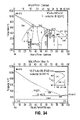
- FIG. 34 is a diagram of gold-based metals having an eutectic ° T of less than 400° C.
- FIG. 35 illustrates the bonding of the base wafer to the cap wafer.
- FIG. 24 shows an example of a two polysilicon surface micromachining process used to fabricate the base wafer of MEMS devices whose mechanical components are to be released by vapor HF (hydrofluoric acid).
- the process starts with a silicon wafer 10 at step a.
- An oxide layer 11 is grown on the wafer 10 , and this is patterned (step b).
- a first polysilicon layer 12 is deposited on the oxide layer 11 and patterned (step c).
- a sacrificial oxide layer 13 is deposited and patterned (step d). This step is followed by deposition of a second polysilicon 14 and stress relief (step e).
- a metal-based interconnect layer 15 is applied and patterned.
- a deep reactive ion etch is carried out to form cavities 16 in the layer 14 extending down to the sacrificial oxide layer 13 .
- Metal layer 15 forms a bond pad 15 a located outside the area to be sealed and an interconnect ring 15 b that forms the basis of a metal-based sealing ring.
- Remaining segments 14 a , 14 b of the second polysilicon layer 14 form the mechanical components that are to be sealed inside the wafer-level package and which are subsequently released with HF, which etches away the sacrificial layer 13 .
- the result of this surface micromachining process produces a series MEMS devices distributed on the surface of the base wafer and incorporating mechanical components yet to be released by vapor HF.
- the structure of the MEMS device is not critical to the invention. It will be understood by one skilled in the art that many other types of structure can be made.
- the three main components of interest at this point of the fabrication of the base wafer are at least one bond pad 15 a , which is located outside the device's area to be sealed in the wafer-level package and electrically connected to components inside the device's area to be sealed in the wafer-level package using an electrical connection made using one of the polysilicon layers below the top polysilicon layer (This connection is not shown in FIG. 24 ).
- This bond pad 15 a is used to electrically connect the MEMS device to the outside world.
- This pad is typically made of an aluminum alloy, of copper or of gold. An example of such bond pad is shown in FIG. 25 .
- the novel metal-based interconnect ring 15 b which is to become the basis of the novel metal-based sealing ring, is patterned simultaneously with the bond pad 15 a and could be made of an aluminum alloy of copper or gold.
- Aluminum alloy and copper are not suitable materials to be exposed to vapor HF.
- Gold is a suitable material to be exposed to vapor HF.
- CMOS fabrication equipment deposition equipment, photoresist coat equipment, photoresist exposure equipment, photoresist develop equipment, etch equipment, photoresist strip equipment and surface cleaning equipment and others
- the preferred metals for the metal-based interconnect ring are aluminum alloy and copper. In the case of integrated optional sensing, control or communication devices and optional high-voltage actuation drivers, this metal-based interconnect ring may also be one of the interconnect layers of these devices or drivers. However, since aluminum alloy or copper are not suitable metals to be exposed to vapor HF, further processing is required before exposure to vapor HF.
- the mechanical components 14 a , 14 b located inside the region to be sealed in the wafer-level package and yet to be released with vapor HF are typically patterned using Deep Reactive Ion Etching (DRIE) and may provide significant topology because these mechanical components may be fabricated with thick polysilicon layer(s).
- DRIE Deep Reactive Ion Etching
- An example of such high topology mechanical components obtained from a 10 ⁇ m thick polysilicon layer is shown in FIG. 26 .
- FIG. 27 shows the top view of a MEMS devices whose mechanical components are yet to be released by vapor HF.
- This top view also shows the three components of interest at this point of the fabrication of the base wafer, namely the bond pads located outside the device's area to be sealed in the wafer-level package; the novel metal-based interconnect ring 15 b , which is to become the basis of the new metal-based sealing ring; and the mechanical components 14 a , 14 b located inside the device's area to be sealed in the wafer-level package and yet to be released with vapor HF.
- the mechanical components 14 a , 14 b are typically patterned using Deep Reactive Ion Etching (DRIE).
- DRIE Deep Reactive Ion Etching
- FIG. 28 shows the novel process steps added to the surface micromachining process flow of FIG. 24 to prepare the base wafer for low temperature bonding.
- a protection photoresist layer 20 is coated, exposed and developed to expose the regions to be plated. These regions include the bond pads and the new metal-based interconnect ring.
- the photoresist thickness is adjusted to protect adequately the topology created from the DRIE of the polysilicon layer 14 .
- the thicker the polysilicon the thicker this protection photoresist.
- the temperature and duration of the post-develop bake of the photoresist are adjusted as to allow the photoresist to resist the subseqent cleaning and plating processes (step b).
- the photoresist layer 20 is exposed using a mask (not shown) which allows the bond pads 15 a and the metal-based interconnect ring 15 b to be opened over a wider area than their actual dimensions.
- the larger opening of the bond pads and of the metal-based interconnect ring permits the plating of the aluminum or copper sidewalls and protects the aluminum or copper during the subsequent vapor HF exposure.
- the technique described in this document can be applied to the wafer-level packaging of MEMS devices following proper cleaning of the aluminum (copper) surface, following proper aluminum (copper) de-oxydation using, for example, a diluted nitric acid to prepare the aluminum (copper) surface of the complete batch of twenty-four wafers for the application of a the zinc (palladium) catalyst, and following a light sulfuric or hydrofluoric acid dip to remove the catalyst from all non-aluminum (non-copper) exposed surfaces.
- the autocatalytic electroless plating of a 1.0 to 3.0 ⁇ m thick nickel barrier layer 21 (step b) is performed in the exposed catalyzed regions on this complete batch of twenty-four wafers at a temperature of about 90° C.
- this electroless plating technique allows the plating onto the exposed electrically floating aluminum (copper) electrodes without having to be concerned about electrical connections. This is an important feature because it avoids the use of an electrical seed layer which would be very difficult to completely remove (at a later time in the process) from the sidewalls of structures similar to the ones shown in FIG. 26 prior the vapor HF release of the structures.
- Stapleton Tech's Micro 282SX is an example of sodium-free, potassium-free and lithium-free acidic chemistry which can prevent mobile ion contamination and allow the integration of optional sensing, control or communication devices and optional high-voltage actuation drivers.
- This example of mobile ion-free electrolytic nickel chemistry contains a source of nickel ions, a source of phosphorus and a dimethylamine borane reducing agent providing a vapor HF-resistant nickel-phosphorus diffusion barrier alloy protecting the underlying aluminum (copper) to react with the upper gold layer during bonding and during higher temperature exposures of the MEMS device in the field.
- a very thin layer (0.15 to 0.25 ⁇ m) of 24 kt pure soft gold 30 is then deposited in the exposed regions on the complete batch of twenty-four wafers (step c) over the selective nickel layer using immersion plating at a temperature of about 90° C. and at a rate of about 2 ⁇ m/hour using no electrical bias.
- the minimum thickness of 0.15 ⁇ m is designed to prevent the diffusion of nickel through the gold layer and its accumulation on the gold bonding surface.
- this immersion plating technique allows gold to be selectively deposited onto the exposed electrically floating nickel plated electrodes without having to be concerned about biasing the electrodes.
- This feature is also important because it also avoids the use of a nickel or gold seed layer which would be very difficult to completely remove (at a later time in the process) from the sidewalls of structures similar to the ones shown in FIG. 26 and which would block the vapor HF release of the structures.
- This gold layer prevents the oxidation of nickel and provides a stable and repeatable surface composition to bond to. This alleviates the previously discussed problems related to the natural oxidation of the bonding surfaces of the base wafer.
- Cyanide-free sulfite-based chemistries such as Stapleton Tech's Micro 294, or other sodium-free, potassium-free and lithium-free chemistries prevent mobile ion contamination and allow the integration of optional sensing, control or communication devices and optional high-voltage actuation drivers.
- the protection photoresist is stripped using an oxygen plasma (step d). Because gold is a noble metal, this exposure to an oxygen plasma will not oxidize its surface. This stable gold surface situation contrasts with the process described in U.S. Pat. No. 5,668,033 (Nippon Denso Co., Ltd.) Prior Art which discloses the use of the oxygen-unstable silicon surface into a silicon-gold eutectic bonding process.
- the improved gold-exposed surface of the base wafer prevents natural re-oxidation and prevents oxygen plasma-induced oxidation of the bonding surface, thus eliminating restrictions concerning the impact of the time delay required between steps, during manipulation and while successively bonding all of the forty-eight wafers (one set of twenty-four cap wafers to bound to one set of twenty-four base wafers).
- the vapor HF mechanical release of the mechanical components located inside the area to be sealed in the wafer-level package can be performed (step e).
- FIG. 29 is an example of a released structure whose sacrificial oxide has been completely removed using vapor HF. Since immersion gold and electroless nickel are both inert in vapor HF, and since nickel overlaps the underlying aluminum bond pads and interconnect ring, the aluminum (or copper)—electroless nickel—immersion gold structure is not affected by a long exposure to vapor HF and the top bonding surface remain oxide-free, ready for a reliable bonding to the cap wafer.
- the barrier layer 21 is optional.
- the barrier layer can be made of a material selected from the group consisting of: titanium, Ti, tantalum, Ta, platinum, Pt, rhodium, Rh, palladium, Pd, ruthenium, Ru, titanium tungsten, TiW, titanium tungsten nitride TiW(N), titanium nitride, TiN, titanium carbide, TiC, titanium boride, TiB, tungsten nitride, WN, tungsten carbide, WC, tungsten boride, WB, tantalum nitride, TaN, tantalum carbide, TaC, tantalum boride, TaB, halfmium nitride, HfN, halfmium carbide, HfC, halfmium boride, HfB, or tungsten silicon nitride, WsiN.
- a spacer layer can be optionally deposited under the barrier layer 21 .
- the spacer layer can be made of a material selected from the group consisting of: gold, Au, nickel, Ni, nickel-phosphorus, Ni(P), nickel-palladium, Ni(Pd), chromium, Cr, copper, Cu, bismuth, Bi, cadmium, Cd or palladium-cobalt, PdCo.
- the spacer layer is preferably deposited by electroless plating, but can also be deposited by auto-catalytic plating, electrolytic plating, electroplating method, evaporation, electron beam deposition, a lift-off technique, sputtering, chemical vapor deposition (CVD), plasma enhanced chemical vapor deposition (PECVD) or metallorganic chemical vapor deposition (MOCVD).
- CVD chemical vapor deposition
- PECVD plasma enhanced chemical vapor deposition
- MOCVD metalorganic chemical vapor deposition
- FIGS. 30 a and 30 b illustrate the fabrication process of the cap wafer.
- a flat, 300 to 675 ⁇ m thick, high resistivity silicon wafer 50 of low enough carrier concentration to be transparent in the C-Band (1300 nm), L-Band (1550 nm) and L-Band (1625 nm) infrared optical telecommunication bands is thermally oxidized on both faces to generate a 0.1 to 1.0 ⁇ m thick oxide hard mask 51 , 52 for the subsequent silicon machining.
- Standard photolithography is performed to expose the silicon wafer 50 outside the region to be sealed with the wafer-level packaging (step b).
- a deep machining of the silicon is performed to achieve a silicon thickness about half of the original silicon thickness over a portion 53 of the wafer outside the region to be sealed with the wafer-level packaging.
- Dry DRIE or wet KOH or TMAH can be used. If wet KOH and TMAH is used, special precautions should be taken as to take into account the type of silicon wafer, its crystal orientation and the alignment of the mask openings to the actual crystal lattice to achieve the desired final width at the desired final etched thickness.
- a removal of the thermal oxide hard mask is performed using a wet HF solution as to leave a clean, residue-free silicon surface (step d).
- a 0.05 to 1.0 ⁇ m thick sodium-free, potassium-free and lithium-free barrier metal 54 is deposited (step e).
- This barrier metal prevents the formation of intermetallic compounds by limiting the interaction of the underlying silicon wafer with the overlying seed layer and plated layers during the bonding process and during high temperature operation of the MEMS device in the field.
- barrier metals include titanium, Ti, titanium-tungsten, TiW, nickel, Ni, chromium, Cr, titanium nitride, TiN, alloys of these, compound structures of these, or other barrier metals known to limit the reactivity of gold to silicon;
- a 0.05 to 1.0 ⁇ m thick sodium-free, potassium-free and lithium-free seed layer 55 is deposited (step f), preferably in-situ on the previously deposited barrier metal.
- This barrier metal allows the subsequent electrolytic plating to be easily performed in windows to be opened through the following plating mask.
- This seed layer 55 should be selected to prevent the natural oxidation of its surface. Examples of such seed layers involve gold, Au, nickel/gold structures, Ni/Au, platinum, Pt, rhodium, Rh, alloys of these, compound structures of these, or other noble metals known to be resistant to oxidation.
- a 1.0 to 100.0 ⁇ m thick plating mask 56 is coated, exposed and developed to open windows to be plated with the following metals, using electrolytic plating. Unlike autocatalytic electroless plating and immersion plating, the electrolytic plating requires this seed layer to be exposed at the bottom of each window to be electrically connected so as to initiate and maintain the plating process.
- the mask pattern on this cap wafer should be the mirror image of the mask pattern of the sealing metal ring of the base wafer. It should be noted at this point that the regions symmetrical to the bond pads of the base wafers are not to be opened through this plating mask, and thus not to be plated on the cap wafer.
- Typical plating masks are high quality photoresists and polymers such as one known under the trade designation SU-8, available from MicroChem Inc, of Newton, Mass. The required thickness to be plated is dependant upon the nature of the underlying MEMS mechanism to protect and is basically only limited by the thickness of the plating mask;
- a 1.0 to 75.0 ⁇ m thick electrolytic nickel layer 57 is plated from sodium-free, potassium-free and lithium-free nickel sulfamate, Ni(NH 2 SO 3 ) 2 , nickel chloride, NiCl 2 .6H 2 O and boric acid, H 3 BO 3 , or, alternately, nickel sulfate, NiSO 4 .6H 2 O, nickel chloride and boric acid over the seed layer 56 in the opened windows of the plating mask (step h).
- the electrolytic plating of nickel is performed at a temperature of 55° C., at a current density of about 70 mA/cm 2 , at a nickel metal concentration of about 335 g/l, at an acid pH value of about 4.0, can produce a semi-bright electrolytic nickel plating at a rate of about 0.75 ⁇ m/minute. See, for example, G. Di Bari, “Nickel Plating”, ASM Handbook, Vol 5, Surface Engineering, ASM International, Materials Park, Ohio 44073,1994, p.201.
- a very thin layer (0.15 to 0.25 ⁇ m) of 24 kt pure soft gold 58 is then deposited over the nickel layer 57 (step i) using electrolytic plating from sodium-free, potassium-free and lithium-free ammonium gold sulfite electrolyte, (NH 4 ) 3 [Au(SO 3 )] at a temperature of about 55° C., at a current density of about 7.5 mA/cm 2 , at a gold metal concentration of about 12 g/l, at a neutral pH value of 7.0 can produce a semi-bright electrolytic gold plating at a rate of about 0.45 ⁇ m/minute.
- the minimum thickness of 0.15 ⁇ m prevents the diffusion of nickel through the gold layer and its accumulation on the gold bonding surface.
- a thin layer 59 of low temperature eutectic metal is deposited by electrolytic plating. Out of all metals used in this new bonding process, this low temperature eutectic metal is the one with the lowest melting temperature. The type of low temperature eutectic metal to be used and its composition will control the bonding temperature of the base wafer to the cap wafer.
- the most common low temperature eutectic metal is the lead-tin eutectic solder (37.1% Pb73.9% Sn).
- FIG. 31 shows the lead-tin phase diagram which indicates that an eutectic temperature as low as 183° C. is associated to the 37.1% Pb-73.9% Sn eutectic alloy. This low eutectic temperature of 183° C. is interesting. However, since there is much pressure to convert all manufacturing processes to lead-free processes, an alternate low temperature eutectic metal is preferably selected.
- FIG. 32 shows tin-based metals having an eutectic ° T of less then 400° C., namely Tin-Gold, with a 20% Sn-80% Au eutectic point @ 282° C.; Tin-Silver; with a 96.2% Sn-3.8% Ag eutectic point @ 221° C.; Tin-Aluminum, with a 97.6% Sn-2.4% AI eutectic point @ 228° C.; Tin-Copper, with a 98.7% Sn-1.3% Cu eutectic point @ 227° C.; Tin-Nickel, with a 99.9% Sn-0.1% Ni eutectic point @ 231° C.; and Tin-Silicon, with a 99.9% Sn-0.1% Si eutectic point @ 232° C.
- Tin-Gold with a 20% Sn-80% Au eutectic point @ 282° C.
- Tin-Silver with a 96
- FIG. 33 shows that the Tin-Gold system is particularly interesting because the large proportion of gold in the 20% Sn-80% Au 282° C. eutectic composition and the large proportion of tin in the 93% Sn-7% Au 217° C. eutectic indicate that pressing a pure layer of gold against a pure layer of tin at a temperature much higher then 282° C. and cooling toward 282° C.
- the plating of a pure tin layer of optimized thickness (about 0.1 ⁇ m to completely consume the 0.2 ⁇ m of gold from the cap wafer and the 0.2 ⁇ m of gold from the base wafer and form a 20% Sn-80% Au eutectic) over the gold layer of the cap wafer will result in the formation of an excellent bond when this tin layer will be pressed at high temperature between the gold layer of the cap wafer and the gold layer of the base wafer.
- this pure tin layer allows the formation of the 20% Sn-80% Au eutectic layer from the diffusion bonding to and/or from the upper and lower gold layers.
- FIG. 34 shows the gold-based metals having an eutectic ° T of less than 400° C., namely: Gold-Tin, with a 80% Au-20% Sn eutectic point @ 282° C.; Gold-Cadmium, with a 6% Au-94% Cd eutectic point @ 309° C.; and Gold-Bismuth, with a 13.2% Au-86.8% Bi eutectic point @ 241° C.
- the Gold-Cadmium and Gold-Bismuth systems are also particularly interesting because the large proportion of gold in the 6% Au-94% Cd eutectic composition and in the 13.2% Au-86.8% Bi eutectic composition also indicate that pressing a pure layer of gold against a pure layer of cadmium at a temperature much higher than 309° C. and cooling toward 309° C. or of bismuth at a temperature much higher than 241° C. and cooling of toward 241° C.
- the bismuth can also be present as an alloy or compound.
- the plating of a pure cadmium layer of optimized thickness (about 6.3 ⁇ m to completely consume the 0.2 ⁇ m of gold from the cap wafer and the 0.2 ⁇ m of gold from the base wafer and form a 6% Au-94% Cd eutectic) over the gold layer of the cap wafer will result in the formation of an excellent bond when this cadmium layer will be pressed at high temperature between the gold layer of the cap wafer and the gold layer of the base wafer.
- the plating of a pure bismuth layer of optimized thickness (about 2.6 ⁇ m as to completely consume the 0.2 ⁇ m of gold from the cap wafer and the 0.2 ⁇ m of gold from the base wafer and form a 13.2% Au-86.8% Bi eutectic) over the gold layer of the cap wafer will result in the formation of an excellent bonding when this bismuth layer will be pressed at high temperature between the gold layer of the cap wafer and the gold layer of the base wafer
- the low temperature eutectic metal to be deposited by electrolytic plating over the 0.2 ⁇ m thick 24 kt pure soft gold could then be approximately 0.1 ⁇ m thick for tin, a 6.3 ⁇ m thick for cadmium or 2.6 ⁇ m thick for bismuth.
- the result is a diffusion bonding of the metal layer to the upper and lower gold layer.
- the plating mask is removed using an oxygen plasma in step k. Since the 0.1 ⁇ m thick tin, the 6.3 ⁇ m thick cadmium or the 2.6 ⁇ m thick bismuth is exposed to the oxygen plasma during this mask removal, a protective photoresist layer 60 is coated, exposed and developed to protect the 0.1 ⁇ m thick tin, the 6.3 ⁇ m thick cadmium or the 2.6 ⁇ m thick bismuth low temperature eutectic metal during the removal of the seed layer and of the diffusion barrier layer.
- the seed layer 55 is removed by wet etching at step m.
- the barrier metal layer 54 is removed by wet etching at step n to leave a clean silicon surface 61 in the region to be sealed with the wafer-level package. This allows the cap wafer to be transparent in the infrared region of the electromagnetic spectra and allows the fabrication of high performance Photonics MEMS.
- the photoresist layer 60 protecting the 0.1 ⁇ m thick tin, the 6.3 ⁇ m thick cadmium or the 2.6 ⁇ m thick bismuth low temperature eutectic metal is removed. Special precautions should be taken to reduce the natural oxide that grows on the surface of these layers prior the bonding to avoid blocking the bonding reaction.
- the cap wafer is now ready for bonding to the base wafer.
- the bonding process can be performed in a commercial system such as the Electro Vision EVG-560.
- the bonding sequence involves:
- step a shown in FIG. 35 the alignment of the gold metal ring of the base wafer to the low temperature eutectic metal of the bonding ring of the cap wafer.
- a vacuum degassing operation is performed at a temperature slightly higher than the gold-metal eutectic temperature and for a long enough period of time to sufficiently degas the materials to be sealed in the cavity but short enough to prevent excessive reaction between the low temperature eutectic layer and the gold layer of the cap wafer.
- step b the gas mixture is set at the desired pressure or the vacuum is set at the desired value before contacting the two wafers.
- a force is applied to the two wafers so as to force the liquid eutectic mixture of the bonding ring to closely contact the gold ring of the base wafer.
- a typical force of about 2–10 N/(mm 2 of physical contact area) is applied and held so as to allow the diffusion bonding of the two substrates to be completed (i.e. allow the tin, cadmium or bismuth material to have completed its reaction with the 0.2 ⁇ m thick underlying gold layer and the 0.2 ⁇ m thick overlying gold layer.
- the pair of wafers is cooled below the eutectic point, thus preventing a potential de-bonding during cooling. The force is relieved and the pair of wafers is unloaded.
- step c backgrinding and/or polishing of the back side of the cap wafer (now the top side of the bonded pair of wafers) is performed to completely expose the region outside the sealed cavity.
- a high etch rate TMAH, a high etch rate Deep Reactive Ion Etch (DRIE) or a combination of these three techniques could be performed in order to eliminate the portion of the cap wafer located outside the Relieve force without any damage to the devices.
- the bonding is complete and the cap wafer is diffusion bonded, or brazed, to the base wafer with a welded interface where the micro-defects have disappeared, thus creating a leak-tight bonding around the vacuum sealed or sealed and controlled ambient cavity.
- the MEMS device is then ready for testing.
- the region Prior to bonding of the base and cap wafers, the region is preferably exposed, at the moment the first wafer contacts the second wafer, to an environment of consisting of a vacuum, or a controlled ambient pressure consisting of an inert gas; an insulating gas, a forming gas; an oxide reduction gas; and a non-inert gas selected to perform a specific function in the cavity to be sealed as to obtain this environment inside said cavity.
- the inert gas can be nitrogen, helium, neon, argon, krypton, xenon or radon.
- the insulating gas can be sulfur hexafluoride (SF 6 ) or freons.
- the forming gas can be hydrogen.
- the temperature of the base wafer is higher than the temperature of the cap wafer to ensure proper degassing of the components located in the formed cavity.
- the liquid solution of the surface of the cap wafer is preferably permitted to fill microscopic defects, microscopic cracks, microscopic dimples, or microscopic depressions induced by the gold surface roughness of the base wafer.
- intimate contact between the liquid solution of the first wafer and the higher temperature gold, gold alloy or gold compound layer of the base wafer causes at least partial dissolution of the gold, gold alloy or gold compound layer of the first wafer into the liquid solution at the interface, thus increasing the proportion of gold in the liquid solution while reducing the amount of gold, gold alloy or gold compound of the first wafer.
- the temperature of the first and second wafers should preferably maintained while they are in contact with each other for a certain period of time so as to allow even more dissolution of the gold, gold alloy or gold compound layer of the base wafer to be dissolved into the liquid solution filling the micro-defects of the interface between the first wafer and second wafer. This period can be made long enough for additional dissolution of the gold, gold alloy or gold compound layer of the first wafer to be dissolved into the liquid solution filling the micro-defects of the interface between the two wafers.
- the dissolution of the gold, gold alloy or gold compound layer of the first wafer can cause the complete consumption of the under-layer of gold, gold alloy or gold compound in the second wafer while maintaining the gold-enriched solution in a liquid state.
- the initial amount of gold, gold alloy or gold compound underlying the bismuth, bismuth alloy or bismuth compound over-layer of the cap wafer, the initial amount of gold, gold alloy or gold compound of the base wafer and the temperature of the contacted first wafer and second wafer define the actual composition of the liquid solution present at the vanishing interface and micro-defects.
- the temperature of the contacted wafers should be such that, for the actual composition of the liquid solution defining the actual liquidus temperature of the gold-bismuth phase diagram, it approaches the liquidus temperature below which the first gold crystals or gold-bismuth intermetallic crystals will begin to precipitate.
- the temperature of the first wafer and second wafer is reduced after contact to cause the crystallization of crystals having a richer content of the material of the over-layer.
- the material of the over-layer should be reduced to the lowest liquidus of the appropriate phase diagram.
- the temperature is reduced to the lowest temperature liquidus of the gold-bismuth phase diagram, namely 241° C., where liquid phase has completely disappeared with the formation of crystals of 13.2% Au/86.8% Bi composition.
- the material of the over-layer is cadmium, cadmium alloy or cadmium compound
- the temperature is reduced to the lowest temperature liquidus of the gold-bismuth phase diagram, namely 309° C., where liquid phase has completely disappeared with the formation of crystals of 6% Au/94% Cd composition.
- the temperature is reduced to the lowest temperature liquidus of the gold-tin phase diagram, namely 282° C. (for 80% Au/20% Sn) or 217° C. (for 7% Au/93% Sn), where liquid phase has completely disappeared with the formation of crystals of 80% Au/20% Sn or of 7% Au/93% Sn composition.
- the temperature of the bonded wafers is then reduced to room temperature and the cap wafer is micro-machined without damaging the underlying base wafer so as to remove the portion of the cap wafer outside the sealed cavity and to expose the region of the base wafer outside the cavity without damaging the seal of the cavity.
- the micro-machining involves the use of one or more processes including grinding, polishing, a wet etch in TMAH, KOH, EDP, a plasma etch, a reactive ion etch, RIE, a deep reactive ion etch, DRIE, a mechanical blasting technique using silicon carbide, SiC other micro-beeds to remove the portion of the cap wafer outside the sealed cavity.
- the obtained micro-machined bonded wafers result in a wafer-level packaged wafer.
- the wafer-level packaged wafer may incorporate one or more components including a silicon semiconductor device, a germanium semiconductor device, a silicon-germanium semiconductor device, a III–V compound semiconductor, optical device, a II–VI compound semiconductor, a silica photonic device, a plastic photonic device, a CMOS, DMOS, BCDMOS, Bipolar, BICMOS or other high-voltage driver or device, a micro-electro-mechanical system, a sensor, an actuator, an intelligent microsystem, a biochip, a laboratory on a chip, LOAC.
- a silicon semiconductor device a germanium semiconductor device, a silicon-germanium semiconductor device, a III–V compound semiconductor, optical device, a II–VI compound semiconductor, a silica photonic device, a plastic photonic device, a CMOS, DMOS, BCDMOS, Bipolar, BICMOS or other high
- the wafer-level package allows at least one bonding pad located outside the sealed cavity to electrically thermally connect at least one component located the inside the sealed cavity.
- the back side of the base wafer can be subjected polishing and grinding to reduce the overall thickness thereof.
- the wafer-level package can then be diced by standard or slightly modified standard dicing techniques. The individual dies are then packaged in standard molded plastic packages and/or other standard packages.
Abstract
Description
Claims (55)
Priority Applications (3)
| Application Number | Priority Date | Filing Date | Title |
|---|---|---|---|
| US10/310,814 US7138293B2 (en) | 2002-10-04 | 2002-12-06 | Wafer level packaging technique for microdevices |
| EP03103676A EP1405821B1 (en) | 2002-10-04 | 2003-10-03 | Method of fabricating an integrated circuit and its precursor assembly |
| DE60329060T DE60329060D1 (en) | 2002-10-04 | 2003-10-03 | Manufacturing process of an integrated circuit and its precursor |
Applications Claiming Priority (2)
| Application Number | Priority Date | Filing Date | Title |
|---|---|---|---|
| US41578202P | 2002-10-04 | 2002-10-04 | |
| US10/310,814 US7138293B2 (en) | 2002-10-04 | 2002-12-06 | Wafer level packaging technique for microdevices |
Publications (2)
| Publication Number | Publication Date |
|---|---|
| US20040067604A1 US20040067604A1 (en) | 2004-04-08 |
| US7138293B2 true US7138293B2 (en) | 2006-11-21 |
Family
ID=32045019
Family Applications (1)
| Application Number | Title | Priority Date | Filing Date |
|---|---|---|---|
| US10/310,814 Expired - Lifetime US7138293B2 (en) | 2002-10-04 | 2002-12-06 | Wafer level packaging technique for microdevices |
Country Status (3)
| Country | Link |
|---|---|
| US (1) | US7138293B2 (en) |
| EP (1) | EP1405821B1 (en) |
| DE (1) | DE60329060D1 (en) |
Cited By (30)
| Publication number | Priority date | Publication date | Assignee | Title |
|---|---|---|---|---|
| US20040100164A1 (en) * | 2002-11-26 | 2004-05-27 | Murata Manufacturing Co., Ltd. | Manufacturing method of electronic device |
| US20070031994A1 (en) * | 2005-08-03 | 2007-02-08 | Wei-Chung Wang | Method for Fabricating Protective Caps for Protecting Elements on a Wafer Surface |
| US20070045781A1 (en) * | 2005-08-26 | 2007-03-01 | Innovative Micro Technology | Hermetic interconnect structure and method of manufacture |
| US20070269926A1 (en) * | 2006-05-16 | 2007-11-22 | Schultz Peter S | Method and apparatus for forming an electrical connection to a semiconductor substrate |
| US20080048818A1 (en) * | 2006-08-25 | 2008-02-28 | Hong Mao | Transformers with improved voltage-step-down ratios and DC-to-DC power converters employing same |
| US20080274372A1 (en) * | 2005-06-15 | 2008-11-06 | Danfoss A/S | Corrosion Resistant Object Having an Outer Layer of a Precious Metal |
| US20080291938A1 (en) * | 2006-09-29 | 2008-11-27 | Gerald Eckstein | Connecting Device for Randomly Connecting a Number of Transmitters and Receivers, Communication Device and Method for Producing Connecting Device |
| US20090233395A1 (en) * | 2006-06-14 | 2009-09-17 | Magnachip Semiconductor Ltd. | Package of MEMS device and method for fabricating the same |
| US20100084752A1 (en) * | 2008-10-08 | 2010-04-08 | Honeywell International Inc. | Systems and methods for implementing a wafer level hermetic interface chip |
| US20100244159A1 (en) * | 2009-03-30 | 2010-09-30 | Freescale Semiconductor, Inc. | Eutectic flow containment in a semiconductor fabrication process |
| US20100320595A1 (en) * | 2009-06-22 | 2010-12-23 | Honeywell International Inc. | Hybrid hermetic interface chip |
| CN102084505A (en) * | 2008-03-17 | 2011-06-01 | 皇家飞利浦电子股份有限公司 | Underfill process for flip-chip LEDs |
| US20110133294A1 (en) * | 2009-12-08 | 2011-06-09 | Woo Tae Park | Micro electromechanical systems (mems) having a gap stop and method therefor |
| US20110132655A1 (en) * | 2008-08-21 | 2011-06-09 | Murata Manufacturing Co., Ltd. | Electronic Component Device and Method for Manufacturing the Same |
| US20110132656A1 (en) * | 2008-08-21 | 2011-06-09 | Murata Manufacturing, Co., Ltd. | Electronic Component Device and Method for Manufacturing the Same |
| US20110210435A1 (en) * | 2008-11-10 | 2011-09-01 | Nxp B.V. | Mems devices |
| US20110221042A1 (en) * | 2010-03-11 | 2011-09-15 | Freescale Semiconductor, Inc. | Semiconductor device and method of fabricating same |
| US8191756B2 (en) | 2004-11-04 | 2012-06-05 | Microchips, Inc. | Hermetically sealing using a cold welded tongue and groove structure |
| CN101687629B (en) * | 2007-06-29 | 2012-07-18 | 诺思罗普·格鲁曼·利特夫有限责任公司 | Method for the production of a component, and component |
| US8546240B2 (en) | 2011-11-11 | 2013-10-01 | International Business Machines Corporation | Methods of manufacturing integrated semiconductor devices with single crystalline beam |
| US8629036B2 (en) | 2011-11-11 | 2014-01-14 | International Business Machines Corporation | Integrated semiconductor devices with amorphous silicon beam, methods of manufacture and design structure |
| US8741738B2 (en) | 2011-06-08 | 2014-06-03 | Taiwan Semiconductor Manufacturing Company, Ltd. | Method of fabrication of a semiconductor apparatus comprising substrates including Al/Ge and Cu contact layers to form a metallic alloy |
| US20140260612A1 (en) * | 2011-11-28 | 2014-09-18 | Hitachi Automotive Systems, Ltd. | Composite Sensor and Method for Manufacturing The Same |
| US9105751B2 (en) | 2011-11-11 | 2015-08-11 | International Business Machines Corporation | Integrated semiconductor devices with single crystalline beam, methods of manufacture and design structure |
| US9133018B2 (en) * | 2009-07-23 | 2015-09-15 | Industrial Technology Research Institute | Structure and fabrication method of a sensing device |
| US9613926B2 (en) | 2014-12-26 | 2017-04-04 | Taiwan Semiconductor Manufacturing Company, Ltd. | Wafer to wafer bonding process and structures |
| US20170274474A1 (en) * | 2014-08-19 | 2017-09-28 | Koninklijke Philips N.V. | Sapphire collector for reducing mechanical damage during die level laser lift-off |
| US20180261715A1 (en) * | 2015-05-13 | 2018-09-13 | Koninklijke Philips N.V. | Sapphire collector for reducing mechanical damage during die level laser lift-off |
| WO2019195334A1 (en) * | 2018-04-03 | 2019-10-10 | Corning Incorporated | Hermetically sealed optically transparent wafer-level packages and methods for making the same |
| US10784234B2 (en) * | 2017-05-16 | 2020-09-22 | Raytheon Company | Die encapsulation in oxide bonded wafer stack |
Families Citing this family (80)
| Publication number | Priority date | Publication date | Assignee | Title |
|---|---|---|---|---|
| US7242099B2 (en) * | 2001-03-05 | 2007-07-10 | Megica Corporation | Chip package with multiple chips connected by bumps |
| US6862934B2 (en) * | 2001-10-05 | 2005-03-08 | The Charles Stark Draper Laboratory, Inc. | Tuning fork gyroscope |
| JP2003198117A (en) * | 2001-12-28 | 2003-07-11 | Matsushita Electric Ind Co Ltd | Soldering method and junction structure body |
| US6953985B2 (en) * | 2002-06-12 | 2005-10-11 | Freescale Semiconductor, Inc. | Wafer level MEMS packaging |
| DE10309677B4 (en) * | 2003-02-27 | 2008-07-03 | Fraunhofer-Gesellschaft zur Förderung der angewandten Forschung e.V. | Microelectromechanical component and method for producing a microelectromechanical component |
| JP4758614B2 (en) * | 2003-04-07 | 2011-08-31 | ローム・アンド・ハース・エレクトロニック・マテリアルズ,エル.エル.シー. | Electroplating composition and method |
| US20040232535A1 (en) * | 2003-05-22 | 2004-11-25 | Terry Tarn | Microelectromechanical device packages with integral heaters |
| US6858475B2 (en) * | 2003-06-30 | 2005-02-22 | Intel Corporation | Method of forming an integrated circuit substrate |
| EP2937897A3 (en) | 2003-09-15 | 2016-03-23 | Nuvotronics LLC | Device package and methods for the fabrication and testing thereof |
| US7723208B2 (en) * | 2003-09-24 | 2010-05-25 | Intel Corporation | Integrated re-combiner for electroosmotic pumps using porous frits |
| US20050093134A1 (en) | 2003-10-30 | 2005-05-05 | Terry Tarn | Device packages with low stress assembly process |
| US7291513B2 (en) * | 2003-12-15 | 2007-11-06 | Dalsa Semiconductor Inc. | Hermetic wafer-level packaging for MEMS devices with low-temperature metallurgy |
| DE102004005361B4 (en) * | 2004-02-03 | 2008-01-17 | Qimonda Ag | Process for the production of metallic interconnects and contact surfaces on electronic components |
| US20090151972A1 (en) * | 2004-05-28 | 2009-06-18 | Stellar Microdevices, Inc. | Cold weld hermetic mems package and method of manufacture |
| KR100605315B1 (en) | 2004-07-30 | 2006-07-28 | 삼성전자주식회사 | Input/output pad structure of integrated circuit chip |
| US7422962B2 (en) * | 2004-10-27 | 2008-09-09 | Hewlett-Packard Development Company, L.P. | Method of singulating electronic devices |
| US7300812B2 (en) | 2004-10-29 | 2007-11-27 | Hewlett-Packard Development Coompany, L.P. | Micro electrical mechanical system |
| US7897436B2 (en) * | 2004-11-26 | 2011-03-01 | Stmicroelectronics, S.A. | Process for packaging micro-components using a matrix |
| US7528061B2 (en) * | 2004-12-10 | 2009-05-05 | L-3 Communications Corporation | Systems and methods for solder bonding |
| US7235750B1 (en) | 2005-01-31 | 2007-06-26 | United States Of America As Represented By The Secretary Of The Air Force | Radio frequency MEMS switch contact metal selection |
| US7601554B1 (en) | 2005-01-31 | 2009-10-13 | The United States Of America As Represented By The Secretary Of The Air Force | Shaped MEMS contact |
| US7358106B2 (en) * | 2005-03-03 | 2008-04-15 | Stellar Micro Devices | Hermetic MEMS package and method of manufacture |
| US20060214266A1 (en) * | 2005-03-23 | 2006-09-28 | Jordan Larry L | Bevel dicing semiconductor components |
| CN100403033C (en) * | 2005-03-23 | 2008-07-16 | 中国电子科技集团公司第四十九研究所 | Bonding technology for silicon micro acceleration transducer |
| US7508063B2 (en) * | 2005-04-05 | 2009-03-24 | Texas Instruments Incorporated | Low cost hermetically sealed package |
| US7408250B2 (en) * | 2005-04-05 | 2008-08-05 | Texas Instruments Incorporated | Micromirror array device with compliant adhesive |
| JP2007027279A (en) | 2005-07-13 | 2007-02-01 | Shinko Electric Ind Co Ltd | Semiconductor device and manufacturing method thereof |
| TWI265579B (en) * | 2005-08-02 | 2006-11-01 | Advanced Semiconductor Eng | Package structure and wafer level package method |
| US7722929B2 (en) * | 2005-08-18 | 2010-05-25 | Corning Incorporated | Sealing technique for decreasing the time it takes to hermetically seal a device and the resulting hermetically sealed device |
| US20070040501A1 (en) * | 2005-08-18 | 2007-02-22 | Aitken Bruce G | Method for inhibiting oxygen and moisture degradation of a device and the resulting device |
| US20080206589A1 (en) * | 2007-02-28 | 2008-08-28 | Bruce Gardiner Aitken | Low tempertature sintering using Sn2+ containing inorganic materials to hermetically seal a device |
| US7829147B2 (en) * | 2005-08-18 | 2010-11-09 | Corning Incorporated | Hermetically sealing a device without a heat treating step and the resulting hermetically sealed device |
| DE102005040789B4 (en) * | 2005-08-29 | 2014-12-24 | Robert Bosch Gmbh | Manufacturing method for a micromechanical component with anodically bonded cap |
| US7408243B2 (en) * | 2005-12-14 | 2008-08-05 | Honeywell International Inc. | High temperature package flip-chip bonding to ceramic |
| TWI283918B (en) * | 2005-12-21 | 2007-07-11 | Siliconware Precision Industries Co Ltd | Electronic carrier board and package structure thereof |
| TWI278081B (en) * | 2005-12-22 | 2007-04-01 | Siliconware Precision Industries Co Ltd | Electronic carrier board and package structure thereof |
| US20100189223A1 (en) * | 2006-02-16 | 2010-07-29 | Steller Micro Devices | Digitally addressed flat panel x-ray sources |
| US20100189222A1 (en) * | 2006-02-16 | 2010-07-29 | Steller Micro Devices | Panoramic irradiation system using flat panel x-ray sources |
| US9324535B2 (en) * | 2006-02-16 | 2016-04-26 | Stellarray, Incorporaated | Self contained irradiation system using flat panel X-ray sources |
| TWI299552B (en) * | 2006-03-24 | 2008-08-01 | Advanced Semiconductor Eng | Package structure |
| US7781697B2 (en) * | 2006-04-10 | 2010-08-24 | Hewlett-Packard Development Company, L.P. | Micro-display and methods |
| DE102006019080B3 (en) * | 2006-04-25 | 2007-08-30 | Fraunhofer-Gesellschaft zur Förderung der angewandten Forschung e.V. | Housing manufacturing method for e.g. infrared sensor, involves enclosing electrical circuit along metal frame, where circuit is isolated along isolating contour that does not cut surface of substrate |
| DE102006023998B4 (en) * | 2006-05-22 | 2009-02-19 | Infineon Technologies Ag | Electronic circuit arrangement and method for producing such |
| CN100449740C (en) * | 2006-06-19 | 2009-01-07 | 上海集成电路研发中心有限公司 | Cooling method for reducing semiconductor device heating, manufacturing method and corresponding semiconductor device |
| US20080048178A1 (en) * | 2006-08-24 | 2008-02-28 | Bruce Gardiner Aitken | Tin phosphate barrier film, method, and apparatus |
| US10266392B2 (en) | 2007-06-07 | 2019-04-23 | E-Pack, Inc. | Environment-resistant module, micropackage and methods of manufacturing same |
| US8049326B2 (en) | 2007-06-07 | 2011-11-01 | The Regents Of The University Of Michigan | Environment-resistant module, micropackage and methods of manufacturing same |
| US8211752B2 (en) * | 2007-11-26 | 2012-07-03 | Infineon Technologies Ag | Device and method including a soldering process |
| KR100959454B1 (en) * | 2007-12-10 | 2010-05-25 | 주식회사 동부하이텍 | Semiconductor device and method for fabricating the same |
| DE102008041674A1 (en) * | 2008-08-28 | 2010-03-04 | Robert Bosch Gmbh | Micromechanical component and corresponding manufacturing method |
| US20100117153A1 (en) * | 2008-11-07 | 2010-05-13 | Honeywell International Inc. | High voltage soi cmos device and method of manufacture |
| US8089144B2 (en) | 2008-12-17 | 2012-01-03 | Denso Corporation | Semiconductor device and method for manufacturing the same |
| US20100190023A1 (en) * | 2009-01-26 | 2010-07-29 | Adam Franklin Gross | Metal bonded nanotube array |
| CN101993031B (en) * | 2009-08-13 | 2014-04-09 | 联华电子股份有限公司 | Protection structure and semiconductor structure of contact pad |
| US10040681B2 (en) * | 2009-08-28 | 2018-08-07 | Miradia Inc. | Method and system for MEMS devices |
| US8709538B1 (en) * | 2009-09-29 | 2014-04-29 | The Boeing Company | Substantially aligned boron nitride nano-element arrays and methods for their use and preparation |
| KR101096548B1 (en) * | 2009-11-06 | 2011-12-20 | 주식회사 비에스이 | Mems microphone and manufacturing method of the same |
| US8518815B2 (en) * | 2010-07-07 | 2013-08-27 | Lam Research Corporation | Methods, devices, and materials for metallization |
| EP2455332B1 (en) * | 2010-11-19 | 2014-02-12 | Imec | Method for producing temporary cap on a MEMS device |
| CN102556944B (en) * | 2010-12-31 | 2014-11-05 | 中芯国际集成电路制造(上海)有限公司 | Production method for MEMS (micro-electromechanical system) device |
| US8754529B2 (en) * | 2011-03-28 | 2014-06-17 | Miradia, Inc. | MEMS device with simplified electrical conducting paths |
| US9278853B2 (en) | 2011-03-28 | 2016-03-08 | Miramems Sensing Technology Co., Ltd. | Manufacturing process of MEMS device |
| TWI425547B (en) * | 2011-05-06 | 2014-02-01 | Nat Chip Implementation Ct Nat Applied Res Lab | Cmos-mems switch structure |
| US8652865B2 (en) | 2011-08-16 | 2014-02-18 | Freescale Semiconductor, Inc. | Attaching a MEMS to a bonding wafer |
| CN103121658B (en) * | 2011-11-21 | 2015-10-28 | 水木智芯科技(北京)有限公司 | The silicon epitaxy manufacture method of capacitive triaxial micro gyroscope |
| TWI476839B (en) * | 2012-07-06 | 2015-03-11 | Univ Nat Chiao Tung | Sub-micro connection method for wafer and connection layer |
| CN103663356A (en) * | 2012-09-05 | 2014-03-26 | 中国科学院微电子研究所 | Method and structure for encapsulating transparent substrate detector chip |
| CN103832969B (en) * | 2012-11-23 | 2016-06-01 | 上海微电子装备有限公司 | A kind of wafer scale bonding method |
| DE102014202220B3 (en) * | 2013-12-03 | 2015-05-13 | Fraunhofer-Gesellschaft zur Förderung der angewandten Forschung e.V. | Method for producing a cover substrate and coated radiation-emitting component |
| KR101907907B1 (en) * | 2014-01-27 | 2018-10-15 | 고쿠리츠켄큐카이하츠호진 상교기쥬츠 소고켄큐쇼 | Package formation method and mems package |
| US9776858B2 (en) | 2014-02-26 | 2017-10-03 | Taiwan Semiconductor Manufacturing Company Limited | Semiconductor arrangement and formation thereof |
| CN104445046B (en) * | 2014-06-24 | 2016-05-18 | 华天科技(昆山)电子有限公司 | Novel wafer level MEMS chip-packaging structure and method for packing thereof |
| CN105987687B (en) * | 2015-02-15 | 2019-06-28 | 水木智芯科技(北京)有限公司 | New silicon nitride obstructs three-axis gyroscope technique |
| DE102015108494B4 (en) | 2015-05-29 | 2024-01-18 | OSRAM Opto Semiconductors Gesellschaft mit beschränkter Haftung | Method for producing a housing cover and method for producing an optoelectronic component |
| US9874693B2 (en) | 2015-06-10 | 2018-01-23 | The Research Foundation For The State University Of New York | Method and structure for integrating photonics with CMOs |
| CN105293419B (en) * | 2015-10-15 | 2016-12-07 | 华东光电集成器件研究所 | A kind of MEMS preventing superposed layer etching injury |
| US10319654B1 (en) | 2017-12-01 | 2019-06-11 | Cubic Corporation | Integrated chip scale packages |
| CN111115549B (en) * | 2018-10-31 | 2022-12-27 | 深圳华大智造极创科技有限公司 | Low temperature packaging structure and method |
| US11355460B1 (en) | 2020-12-07 | 2022-06-07 | Infineon Technologies Ag | Molded semiconductor package with high voltage isolation |
| CN114189995A (en) * | 2021-12-02 | 2022-03-15 | 广州得尔塔影像技术有限公司 | Manufacturing method of circuit board and circuit board |
Citations (7)
| Publication number | Priority date | Publication date | Assignee | Title |
|---|---|---|---|---|
| WO2001098786A1 (en) | 2000-06-21 | 2001-12-27 | Input Output, Inc. | Accelerometer with folded beams |
| WO2002042716A2 (en) | 2000-11-27 | 2002-05-30 | Microsensors Inc. | Wafer eutectic bonding of mems gyros |
| US20020071169A1 (en) | 2000-02-01 | 2002-06-13 | Bowers John Edward | Micro-electro-mechanical-system (MEMS) mirror device |
| US20020096421A1 (en) * | 2000-11-29 | 2002-07-25 | Cohn Michael B. | MEMS device with integral packaging |
| US20020179986A1 (en) * | 1999-10-04 | 2002-12-05 | Orcutt John W. | MEMS wafer level package |
| US20030116845A1 (en) * | 2001-12-21 | 2003-06-26 | Bojkov Christo P. | Waferlevel method for direct bumping on copper pads in integrated circuits |
| US20030151479A1 (en) * | 2001-09-17 | 2003-08-14 | John Stafford | Latching micro magnetic relay packages and methods of packaging |
Family Cites Families (1)
| Publication number | Priority date | Publication date | Assignee | Title |
|---|---|---|---|---|
| JPH06328617A (en) * | 1993-05-18 | 1994-11-29 | Nippon Steel Corp | Magnesium-aluminum clad material |
-
2002
- 2002-12-06 US US10/310,814 patent/US7138293B2/en not_active Expired - Lifetime
-
2003
- 2003-10-03 EP EP03103676A patent/EP1405821B1/en not_active Expired - Fee Related
- 2003-10-03 DE DE60329060T patent/DE60329060D1/en not_active Expired - Lifetime
Patent Citations (7)
| Publication number | Priority date | Publication date | Assignee | Title |
|---|---|---|---|---|
| US20020179986A1 (en) * | 1999-10-04 | 2002-12-05 | Orcutt John W. | MEMS wafer level package |
| US20020071169A1 (en) | 2000-02-01 | 2002-06-13 | Bowers John Edward | Micro-electro-mechanical-system (MEMS) mirror device |
| WO2001098786A1 (en) | 2000-06-21 | 2001-12-27 | Input Output, Inc. | Accelerometer with folded beams |
| WO2002042716A2 (en) | 2000-11-27 | 2002-05-30 | Microsensors Inc. | Wafer eutectic bonding of mems gyros |
| US20020096421A1 (en) * | 2000-11-29 | 2002-07-25 | Cohn Michael B. | MEMS device with integral packaging |
| US20030151479A1 (en) * | 2001-09-17 | 2003-08-14 | John Stafford | Latching micro magnetic relay packages and methods of packaging |
| US20030116845A1 (en) * | 2001-12-21 | 2003-06-26 | Bojkov Christo P. | Waferlevel method for direct bumping on copper pads in integrated circuits |
Cited By (54)
| Publication number | Priority date | Publication date | Assignee | Title |
|---|---|---|---|---|
| US7259032B2 (en) * | 2002-11-26 | 2007-08-21 | Murata Manufacturing Co., Ltd. | Hermetically sealing a package to include a barrier metal |
| US20040100164A1 (en) * | 2002-11-26 | 2004-05-27 | Murata Manufacturing Co., Ltd. | Manufacturing method of electronic device |
| US8191756B2 (en) | 2004-11-04 | 2012-06-05 | Microchips, Inc. | Hermetically sealing using a cold welded tongue and groove structure |
| US9796583B2 (en) | 2004-11-04 | 2017-10-24 | Microchips Biotech, Inc. | Compression and cold weld sealing method for an electrical via connection |
| US20080274372A1 (en) * | 2005-06-15 | 2008-11-06 | Danfoss A/S | Corrosion Resistant Object Having an Outer Layer of a Precious Metal |
| US20070031994A1 (en) * | 2005-08-03 | 2007-02-08 | Wei-Chung Wang | Method for Fabricating Protective Caps for Protecting Elements on a Wafer Surface |
| US7410886B2 (en) * | 2005-08-03 | 2008-08-12 | Advanced Semiconductor Engineering, Inc. | Method for fabricating protective caps for protecting elements on a wafer surface |
| US7582969B2 (en) * | 2005-08-26 | 2009-09-01 | Innovative Micro Technology | Hermetic interconnect structure and method of manufacture |
| US20070045781A1 (en) * | 2005-08-26 | 2007-03-01 | Innovative Micro Technology | Hermetic interconnect structure and method of manufacture |
| US20070269926A1 (en) * | 2006-05-16 | 2007-11-22 | Schultz Peter S | Method and apparatus for forming an electrical connection to a semiconductor substrate |
| US7524693B2 (en) * | 2006-05-16 | 2009-04-28 | Freescale Semiconductor, Inc. | Method and apparatus for forming an electrical connection to a semiconductor substrate |
| US20090233395A1 (en) * | 2006-06-14 | 2009-09-17 | Magnachip Semiconductor Ltd. | Package of MEMS device and method for fabricating the same |
| US8357560B2 (en) * | 2006-06-14 | 2013-01-22 | Magnachip Semiconductor Ltd. | Package of MEMS device and method for fabricating the same |
| US20080048818A1 (en) * | 2006-08-25 | 2008-02-28 | Hong Mao | Transformers with improved voltage-step-down ratios and DC-to-DC power converters employing same |
| US20080291938A1 (en) * | 2006-09-29 | 2008-11-27 | Gerald Eckstein | Connecting Device for Randomly Connecting a Number of Transmitters and Receivers, Communication Device and Method for Producing Connecting Device |
| US8151444B2 (en) * | 2006-09-29 | 2012-04-10 | Siemens Aktiengesellschaft | Method for manufacturing connecting device for randomly connecting a number of transmitters and receivers |
| CN101687629B (en) * | 2007-06-29 | 2012-07-18 | 诺思罗普·格鲁曼·利特夫有限责任公司 | Method for the production of a component, and component |
| CN102084505B (en) * | 2008-03-17 | 2013-05-01 | 皇家飞利浦电子股份有限公司 | Underfill process for flip-chip LEDs |
| CN102084505A (en) * | 2008-03-17 | 2011-06-01 | 皇家飞利浦电子股份有限公司 | Underfill process for flip-chip LEDs |
| US8273587B2 (en) * | 2008-03-17 | 2012-09-25 | Lumileds Lighting Company Llc | Underfill process for flip-chip LEDs |
| US20110223696A1 (en) * | 2008-03-17 | 2011-09-15 | Koninklijke Philips Electronics N.V. | Underfill process for flip-chip leds |
| US20110132655A1 (en) * | 2008-08-21 | 2011-06-09 | Murata Manufacturing Co., Ltd. | Electronic Component Device and Method for Manufacturing the Same |
| US8558123B2 (en) * | 2008-08-21 | 2013-10-15 | Murata Manufacturing Co., Ltd. | Electronic component device with a Ni-Bi alloy sealing frame |
| US20110132656A1 (en) * | 2008-08-21 | 2011-06-09 | Murata Manufacturing, Co., Ltd. | Electronic Component Device and Method for Manufacturing the Same |
| US8658914B2 (en) * | 2008-08-21 | 2014-02-25 | Murata Manufacturing Co., Ltd. | Electronic component device and method for manufacturing the same |
| US8950067B2 (en) | 2008-08-21 | 2015-02-10 | Murata Manufacturing Co., Ltd. | Method for manufacturing electronic component device with a Ni—Bi alloy sealing frame |
| US20100084752A1 (en) * | 2008-10-08 | 2010-04-08 | Honeywell International Inc. | Systems and methods for implementing a wafer level hermetic interface chip |
| US8980698B2 (en) | 2008-11-10 | 2015-03-17 | Nxp, B.V. | MEMS devices |
| US20110210435A1 (en) * | 2008-11-10 | 2011-09-01 | Nxp B.V. | Mems devices |
| US20100244159A1 (en) * | 2009-03-30 | 2010-09-30 | Freescale Semiconductor, Inc. | Eutectic flow containment in a semiconductor fabrication process |
| US7846815B2 (en) | 2009-03-30 | 2010-12-07 | Freescale Semiconductor, Inc. | Eutectic flow containment in a semiconductor fabrication process |
| US20100320595A1 (en) * | 2009-06-22 | 2010-12-23 | Honeywell International Inc. | Hybrid hermetic interface chip |
| US9133018B2 (en) * | 2009-07-23 | 2015-09-15 | Industrial Technology Research Institute | Structure and fabrication method of a sensing device |
| US20110133294A1 (en) * | 2009-12-08 | 2011-06-09 | Woo Tae Park | Micro electromechanical systems (mems) having a gap stop and method therefor |
| US8119431B2 (en) | 2009-12-08 | 2012-02-21 | Freescale Semiconductor, Inc. | Method of forming a micro-electromechanical system (MEMS) having a gap stop |
| US20110221042A1 (en) * | 2010-03-11 | 2011-09-15 | Freescale Semiconductor, Inc. | Semiconductor device and method of fabricating same |
| US8551814B2 (en) * | 2010-03-11 | 2013-10-08 | Freescale Semiconductor, Inc. | Method of fabricating a semiconductor device that limits damage to elements of the semiconductor device that are exposed during processing |
| US8741738B2 (en) | 2011-06-08 | 2014-06-03 | Taiwan Semiconductor Manufacturing Company, Ltd. | Method of fabrication of a semiconductor apparatus comprising substrates including Al/Ge and Cu contact layers to form a metallic alloy |
| US9059396B2 (en) | 2011-11-11 | 2015-06-16 | International Business Machines Corporation | Integrated semiconductor devices with single crystalline beam, methods of manufacture and design structure |
| US9758365B2 (en) | 2011-11-11 | 2017-09-12 | Globalfoundries Inc. | Integrated semiconductor devices with single crystalline beam, methods of manufacture and design structure |
| US8546240B2 (en) | 2011-11-11 | 2013-10-01 | International Business Machines Corporation | Methods of manufacturing integrated semiconductor devices with single crystalline beam |
| US9105751B2 (en) | 2011-11-11 | 2015-08-11 | International Business Machines Corporation | Integrated semiconductor devices with single crystalline beam, methods of manufacture and design structure |
| US8629036B2 (en) | 2011-11-11 | 2014-01-14 | International Business Machines Corporation | Integrated semiconductor devices with amorphous silicon beam, methods of manufacture and design structure |
| US9172025B2 (en) | 2011-11-11 | 2015-10-27 | Globalfoundries U.S. 2 Llc | Integrated semiconductor devices with single crystalline beam, methods of manufacture and design structure |
| US8921201B2 (en) | 2011-11-11 | 2014-12-30 | International Business Machines Corporation | Integrated semiconductor devices with amorphous silicon beam, methods of manufacture and design structure |
| US20140260612A1 (en) * | 2011-11-28 | 2014-09-18 | Hitachi Automotive Systems, Ltd. | Composite Sensor and Method for Manufacturing The Same |
| US20170274474A1 (en) * | 2014-08-19 | 2017-09-28 | Koninklijke Philips N.V. | Sapphire collector for reducing mechanical damage during die level laser lift-off |
| US11311967B2 (en) * | 2014-08-19 | 2022-04-26 | Lumileds Llc | Sapphire collector for reducing mechanical damage during die level laser lift-off |
| US9613926B2 (en) | 2014-12-26 | 2017-04-04 | Taiwan Semiconductor Manufacturing Company, Ltd. | Wafer to wafer bonding process and structures |
| US20180261715A1 (en) * | 2015-05-13 | 2018-09-13 | Koninklijke Philips N.V. | Sapphire collector for reducing mechanical damage during die level laser lift-off |
| US11342478B2 (en) * | 2015-05-13 | 2022-05-24 | Lumileds Llc | Sapphire collector for reducing mechanical damage during die level laser lift-off |
| US10784234B2 (en) * | 2017-05-16 | 2020-09-22 | Raytheon Company | Die encapsulation in oxide bonded wafer stack |
| WO2019195334A1 (en) * | 2018-04-03 | 2019-10-10 | Corning Incorporated | Hermetically sealed optically transparent wafer-level packages and methods for making the same |
| US11764117B2 (en) | 2018-04-03 | 2023-09-19 | Corning Incorporated | Hermetically sealed optically transparent wafer-level packages and methods for making the same |
Also Published As
| Publication number | Publication date |
|---|---|
| EP1405821A3 (en) | 2004-12-22 |
| EP1405821B1 (en) | 2009-09-02 |
| EP1405821A2 (en) | 2004-04-07 |
| US20040067604A1 (en) | 2004-04-08 |
| DE60329060D1 (en) | 2009-10-15 |
Similar Documents
| Publication | Publication Date | Title |
|---|---|---|
| US7138293B2 (en) | Wafer level packaging technique for microdevices | |
| US9751752B2 (en) | Method of fabrication of Al/Ge bonding in a wafer packaging environment and a product produced therefrom | |
| US7675162B2 (en) | Interconnect structure using through wafer vias and method of fabrication | |
| US8293582B2 (en) | Method of substrate bonding with bonding material having rare Earth metal | |
| US6454160B2 (en) | Method for hermetically encapsulating microsystems in situ | |
| EP1483196B1 (en) | Method of manufacturing deflectable microstructure through bonding of wafers | |
| EP0951068A1 (en) | Method of fabrication of a microstructure having an inside cavity | |
| US8349660B2 (en) | Cavity closure process for at least one microelectronic device | |
| US20020179921A1 (en) | Compliant hermetic package | |
| JP2006116694A (en) | Hermetically sealed microdevice with getter shield | |
| WO2023280676A1 (en) | Use of tin thin film for bonding and as masking film |
Legal Events
| Date | Code | Title | Description |
|---|---|---|---|
| AS | Assignment |
Owner name: DALSA SEMICONDUCTOR INC., CANADA Free format text: ASSIGNMENT OF ASSIGNORS INTEREST;ASSIGNORS:OUELLET, LUC;POISSON, JULES;REEL/FRAME:014076/0275;SIGNING DATES FROM 20030502 TO 20030505 |
|
| STCF | Information on status: patent grant |
Free format text: PATENTED CASE |
|
| FPAY | Fee payment |
Year of fee payment: 4 |
|
| AS | Assignment |
Owner name: TELEDYNE DALSA SEMICONDUCTOR INC., CANADA Free format text: CHANGE OF NAME;ASSIGNOR:DALSA SEMICONDUCTOR INC.;REEL/FRAME:027064/0622 Effective date: 20110214 |
|
| FEPP | Fee payment procedure |
Free format text: PAYOR NUMBER ASSIGNED (ORIGINAL EVENT CODE: ASPN); ENTITY STATUS OF PATENT OWNER: LARGE ENTITY |
|
| FPAY | Fee payment |
Year of fee payment: 8 |
|
| MAFP | Maintenance fee payment |
Free format text: PAYMENT OF MAINTENANCE FEE, 12TH YEAR, LARGE ENTITY (ORIGINAL EVENT CODE: M1553) Year of fee payment: 12 |
|
| AS | Assignment |
Owner name: TELEDYNE DIGITAL IMAGING, INC., CALIFORNIA Free format text: MERGER;ASSIGNOR:TELEDYNE DALSA SEMICONDUCTOR INC.;REEL/FRAME:055434/0643 Effective date: 20210101 |