US7135352B2 - Method of fabricating a cover plate bonded over an encapsulated OLEDs - Google Patents
Method of fabricating a cover plate bonded over an encapsulated OLEDs Download PDFInfo
- Publication number
- US7135352B2 US7135352B2 US10/787,513 US78751304A US7135352B2 US 7135352 B2 US7135352 B2 US 7135352B2 US 78751304 A US78751304 A US 78751304A US 7135352 B2 US7135352 B2 US 7135352B2
- Authority
- US
- United States
- Prior art keywords
- cover plate
- device substrate
- oled devices
- layer
- oled
- Prior art date
- Legal status (The legal status is an assumption and is not a legal conclusion. Google has not performed a legal analysis and makes no representation as to the accuracy of the status listed.)
- Active, expires
Links
- 238000004519 manufacturing process Methods 0.000 title description 4
- 239000000463 material Substances 0.000 claims abstract description 117
- 239000000758 substrate Substances 0.000 claims abstract description 84
- 239000004820 Pressure-sensitive adhesive Substances 0.000 claims abstract description 82
- 238000000034 method Methods 0.000 claims abstract description 50
- 230000001070 adhesive effect Effects 0.000 claims description 32
- 239000000853 adhesive Substances 0.000 claims description 31
- 230000008569 process Effects 0.000 claims description 26
- 239000003795 chemical substances by application Substances 0.000 claims description 14
- 238000004544 sputter deposition Methods 0.000 claims description 4
- 150000001875 compounds Chemical class 0.000 claims description 2
- 230000008020 evaporation Effects 0.000 claims description 2
- 238000001704 evaporation Methods 0.000 claims description 2
- NBVXSUQYWXRMNV-UHFFFAOYSA-N fluoromethane Chemical class FC NBVXSUQYWXRMNV-UHFFFAOYSA-N 0.000 claims description 2
- 238000010438 heat treatment Methods 0.000 claims description 2
- 150000003961 organosilicon compounds Chemical class 0.000 claims description 2
- 229920001296 polysiloxane Polymers 0.000 claims description 2
- 238000007639 printing Methods 0.000 claims description 2
- 238000005507 spraying Methods 0.000 claims description 2
- 238000000151 deposition Methods 0.000 claims 3
- 239000010410 layer Substances 0.000 description 102
- 238000005538 encapsulation Methods 0.000 description 17
- 238000001723 curing Methods 0.000 description 10
- 239000010409 thin film Substances 0.000 description 9
- 238000003475 lamination Methods 0.000 description 7
- 239000012790 adhesive layer Substances 0.000 description 6
- 238000013459 approach Methods 0.000 description 6
- 230000009969 flowable effect Effects 0.000 description 6
- 230000003287 optical effect Effects 0.000 description 6
- 229920000642 polymer Polymers 0.000 description 6
- 239000011347 resin Substances 0.000 description 6
- 229920005989 resin Polymers 0.000 description 6
- 230000007613 environmental effect Effects 0.000 description 5
- 239000003566 sealing material Substances 0.000 description 5
- 239000003463 adsorbent Substances 0.000 description 4
- QVGXLLKOCUKJST-UHFFFAOYSA-N atomic oxygen Chemical compound [O] QVGXLLKOCUKJST-UHFFFAOYSA-N 0.000 description 4
- 230000004888 barrier function Effects 0.000 description 4
- 239000001301 oxygen Substances 0.000 description 4
- 229910052760 oxygen Inorganic materials 0.000 description 4
- 238000004806 packaging method and process Methods 0.000 description 4
- 230000035515 penetration Effects 0.000 description 4
- 238000012546 transfer Methods 0.000 description 4
- 229910052581 Si3N4 Inorganic materials 0.000 description 3
- 230000008901 benefit Effects 0.000 description 3
- 239000000919 ceramic Substances 0.000 description 3
- 239000002800 charge carrier Substances 0.000 description 3
- 238000005520 cutting process Methods 0.000 description 3
- 239000011521 glass Substances 0.000 description 3
- 239000011159 matrix material Substances 0.000 description 3
- TWNQGVIAIRXVLR-UHFFFAOYSA-N oxo(oxoalumanyloxy)alumane Chemical compound O=[Al]O[Al]=O TWNQGVIAIRXVLR-UHFFFAOYSA-N 0.000 description 3
- BPUBBGLMJRNUCC-UHFFFAOYSA-N oxygen(2-);tantalum(5+) Chemical compound [O-2].[O-2].[O-2].[O-2].[O-2].[Ta+5].[Ta+5] BPUBBGLMJRNUCC-UHFFFAOYSA-N 0.000 description 3
- 238000000059 patterning Methods 0.000 description 3
- HQVNEWCFYHHQES-UHFFFAOYSA-N silicon nitride Chemical compound N12[Si]34N5[Si]62N3[Si]51N64 HQVNEWCFYHHQES-UHFFFAOYSA-N 0.000 description 3
- 229910001936 tantalum oxide Inorganic materials 0.000 description 3
- 238000001029 thermal curing Methods 0.000 description 3
- 229920001621 AMOLED Polymers 0.000 description 2
- 238000003848 UV Light-Curing Methods 0.000 description 2
- 238000000231 atomic layer deposition Methods 0.000 description 2
- 230000015556 catabolic process Effects 0.000 description 2
- 238000006731 degradation reaction Methods 0.000 description 2
- 230000000593 degrading effect Effects 0.000 description 2
- 238000010030 laminating Methods 0.000 description 2
- 229910052751 metal Inorganic materials 0.000 description 2
- 239000002184 metal Substances 0.000 description 2
- 230000002093 peripheral effect Effects 0.000 description 2
- 230000005855 radiation Effects 0.000 description 2
- 238000007736 thin film deposition technique Methods 0.000 description 2
- 238000007740 vapor deposition Methods 0.000 description 2
- XLYOFNOQVPJJNP-UHFFFAOYSA-N water Chemical compound O XLYOFNOQVPJJNP-UHFFFAOYSA-N 0.000 description 2
- 239000004831 Hot glue Substances 0.000 description 1
- 238000005299 abrasion Methods 0.000 description 1
- 238000010521 absorption reaction Methods 0.000 description 1
- 239000003522 acrylic cement Substances 0.000 description 1
- 238000004026 adhesive bonding Methods 0.000 description 1
- 239000002390 adhesive tape Substances 0.000 description 1
- 230000002411 adverse Effects 0.000 description 1
- 229910021417 amorphous silicon Inorganic materials 0.000 description 1
- 230000005540 biological transmission Effects 0.000 description 1
- 239000003086 colorant Substances 0.000 description 1
- 239000004020 conductor Substances 0.000 description 1
- 238000010276 construction Methods 0.000 description 1
- 230000008602 contraction Effects 0.000 description 1
- 238000010168 coupling process Methods 0.000 description 1
- 238000005859 coupling reaction Methods 0.000 description 1
- 239000002274 desiccant Substances 0.000 description 1
- 230000000694 effects Effects 0.000 description 1
- 239000007789 gas Substances 0.000 description 1
- 238000010348 incorporation Methods 0.000 description 1
- 239000011261 inert gas Substances 0.000 description 1
- 238000002347 injection Methods 0.000 description 1
- 239000007924 injection Substances 0.000 description 1
- 239000004973 liquid crystal related substance Substances 0.000 description 1
- 230000007246 mechanism Effects 0.000 description 1
- 239000000203 mixture Substances 0.000 description 1
- 238000012986 modification Methods 0.000 description 1
- 230000004048 modification Effects 0.000 description 1
- 239000012044 organic layer Substances 0.000 description 1
- 229920000515 polycarbonate Polymers 0.000 description 1
- 239000004417 polycarbonate Substances 0.000 description 1
- 229920000728 polyester Polymers 0.000 description 1
- 238000003825 pressing Methods 0.000 description 1
- 239000010453 quartz Substances 0.000 description 1
- 238000003847 radiation curing Methods 0.000 description 1
- 230000006798 recombination Effects 0.000 description 1
- 238000005215 recombination Methods 0.000 description 1
- 230000004044 response Effects 0.000 description 1
- 238000007789 sealing Methods 0.000 description 1
- 239000012945 sealing adhesive Substances 0.000 description 1
- VYPSYNLAJGMNEJ-UHFFFAOYSA-N silicon dioxide Inorganic materials O=[Si]=O VYPSYNLAJGMNEJ-UHFFFAOYSA-N 0.000 description 1
- 229910052814 silicon oxide Inorganic materials 0.000 description 1
- -1 silicon-oxinitride Chemical compound 0.000 description 1
- 150000003384 small molecules Chemical class 0.000 description 1
- 238000001228 spectrum Methods 0.000 description 1
- 238000003892 spreading Methods 0.000 description 1
- 230000007480 spreading Effects 0.000 description 1
- 230000000007 visual effect Effects 0.000 description 1
- 238000012800 visualization Methods 0.000 description 1
Images


Classifications
-
- H—ELECTRICITY
- H10—SEMICONDUCTOR DEVICES; ELECTRIC SOLID-STATE DEVICES NOT OTHERWISE PROVIDED FOR
- H10K—ORGANIC ELECTRIC SOLID-STATE DEVICES
- H10K59/00—Integrated devices, or assemblies of multiple devices, comprising at least one organic light-emitting element covered by group H10K50/00
- H10K59/80—Constructional details
- H10K59/87—Passivation; Containers; Encapsulations
- H10K59/871—Self-supporting sealing arrangements
- H10K59/8722—Peripheral sealing arrangements, e.g. adhesives, sealants
-
- H—ELECTRICITY
- H10—SEMICONDUCTOR DEVICES; ELECTRIC SOLID-STATE DEVICES NOT OTHERWISE PROVIDED FOR
- H10K—ORGANIC ELECTRIC SOLID-STATE DEVICES
- H10K50/00—Organic light-emitting devices
- H10K50/80—Constructional details
- H10K50/84—Passivation; Containers; Encapsulations
- H10K50/842—Containers
- H10K50/8426—Peripheral sealing arrangements, e.g. adhesives, sealants
-
- H—ELECTRICITY
- H10—SEMICONDUCTOR DEVICES; ELECTRIC SOLID-STATE DEVICES NOT OTHERWISE PROVIDED FOR
- H10K—ORGANIC ELECTRIC SOLID-STATE DEVICES
- H10K50/00—Organic light-emitting devices
- H10K50/80—Constructional details
- H10K50/84—Passivation; Containers; Encapsulations
- H10K50/841—Self-supporting sealing arrangements
-
- H—ELECTRICITY
- H10—SEMICONDUCTOR DEVICES; ELECTRIC SOLID-STATE DEVICES NOT OTHERWISE PROVIDED FOR
- H10K—ORGANIC ELECTRIC SOLID-STATE DEVICES
- H10K59/00—Integrated devices, or assemblies of multiple devices, comprising at least one organic light-emitting element covered by group H10K50/00
- H10K59/80—Constructional details
- H10K59/87—Passivation; Containers; Encapsulations
- H10K59/871—Self-supporting sealing arrangements
-
- H—ELECTRICITY
- H10—SEMICONDUCTOR DEVICES; ELECTRIC SOLID-STATE DEVICES NOT OTHERWISE PROVIDED FOR
- H10K—ORGANIC ELECTRIC SOLID-STATE DEVICES
- H10K2102/00—Constructional details relating to the organic devices covered by this subclass
- H10K2102/301—Details of OLEDs
- H10K2102/302—Details of OLEDs of OLED structures
- H10K2102/3023—Direction of light emission
- H10K2102/3026—Top emission
-
- H—ELECTRICITY
- H10—SEMICONDUCTOR DEVICES; ELECTRIC SOLID-STATE DEVICES NOT OTHERWISE PROVIDED FOR
- H10K—ORGANIC ELECTRIC SOLID-STATE DEVICES
- H10K71/00—Manufacture or treatment specially adapted for the organic devices covered by this subclass
- H10K71/851—Division of substrate
Definitions
- the present invention relates to environmental protection of top-emitting or bottom-emitting OLED devices.
- OLED organic light-emitting diode
- EL organic electroluminescent
- OLED devices include active matrix image displays, passive matrix image displays, and area lighting devices such as, for example, selective desktop lighting devices. Irrespective of the particular OLED device configuration tailored to these broad fields of applications, all OLEDs function on the same general principles.
- An organic electroluminescent (EL) medium structure is sandwiched between two electrodes. At least one of the electrodes is light transmissive. These electrodes are commonly referred to as an anode and a cathode in analogy to the terminals of a conventional diode. When an electrical potential is applied between the electrodes so that the anode is connected to the positive terminal of a voltage source and the cathode is connected to the negative terminal, the OLED is said to be forward biased.
- EL organic electroluminescent
- Positive charge carriers are injected from the anode into the EL medium structure, and negative charge carriers (electrons) are injected from the cathode.
- Such charge carrier injection causes current flow from the electrodes through the EL medium structure. Recombination of holes and electrons within a zone of the EL medium structure results in emission of light from this zone that is, appropriately, called the light-emitting zone or interface. The emitted light is directed towards an observer, or towards an object to be illuminated, through the light transmissive electrode. If the light transmissive electrode is between the substrate and the light emissive elements of the OLED device, the device is called a bottom-emitting OLED device. Conversely, if the light transmissive electrode is not between the substrate and the light emissive elements, the device is referred to as a top-emitting OLED device.
- the organic EL medium structure can be formed of a stack of sublayers that can include small molecule layers and polymer layers. Such organic layers and sublayers are well known and understood by those skilled in the OLED art.
- top-emitting OLED devices In top-emitting OLED devices, light is emitted through an upper electrode or top electrode which has to be sufficiently light transmissive, while the lower electrode(s) or bottom electrode(s) can be made of relatively thick and electrically conductive metal compositions which can be optically opaque. Consequently, the lower electrodes (anodes) can be formed over relatively complex drive circuitry in an active matrix OLED image display.
- Top-emitting OLED displays offer the potential to improve display performance compared with bottom-emitting OLED displays by:
- bottom-emitting OLED devices continue to find widespread use in displays of data or in the field of advertising.
- Unprotected OLED display devices irrespective of device configuration, are prone to relatively rapid degradation of performance due to adverse effects of moisture and/or oxygen present in the ambient environment. Additionally, unprotected devices can be subject to mechanical damage caused by abrasion.
- Various efforts have been directed at providing packaged OLED displays in which the packaging approaches offer improved operational lifetime of displays which is, however, still limited so that widespread adoption of OLED display devices is currently restricted.
- cover plates which are adhesively bonded over an upper surface of an OLED device.
- Adhesive bonding of a cover plate has been provided in prior art packaging approaches by either forming a perimeter seal for bonding a cover plate along a device perimeter, or by uniformly bonding a cover plate over an entire device area.
- cover plate bonding has been achieved by dispensing a flowable adhesive material on the cover plate or on the upper surface of the OLED device, bringing the cover plate and the device surface in contact, followed by curing the adhesive material by a thermal curing process or by a radiation curing process.
- Maruyama et al. propose a perimeter seal which is formed between two concave grooves disposed near perimeter areas of an OLED device.
- the perimeter seal provides a spacing between a device surface and a surface of a second substrate which functions as a cover plate. This spacing can be filled with an inert gas.
- Maruyama et al. do not suggest or disclose electrical interconnect areas, nor approaches to keep such interconnects free from perimeter seal material.
- Wei et al. disclose a package method and apparatus for organic electroluminescent display.
- a certain amount of an ultraviolet curing resin or thermal curing resin is spread on a lamination plate or a substrate.
- a trench is formed at an edge of the lamination plate.
- the space between the lamination plate and the substrate is controlled by adjusting lamination pressure so that excess resin flows into the trench at the edge of the lamination plate, and the dimensions of the package can be controlled.
- the resin is cured by ultraviolet radiation or by a thermal process.
- Wei et al. provide uniform bonding between the substrate and the lamination plate which functions as a cover plate.
- Wei et al. do not suggest or disclose electrical interconnect areas nor approaches to keep such interconnects free from resins.
- Park et al. disclose a package method and apparatus for organic electroluminescent display.
- a trench is disposed on at least one of the cover plate or device substrate to prevent perimeter sealing material from contacting the display area of the OLED device.
- excess perimeter sealing material resin flows into the trench, and the sealing material is prevented from contacting the display area.
- Park et al. do not suggest or disclose electrical interconnect areas nor approaches to keep such interconnects free from perimeter sealing material.
- Serbicki et al. recognized the importance of keeping at least outermost portions of electrical interconnect areas of OLED devices free from a flowable adhesive material.
- Various configurations of flow-preventing patterns are disclosed which are oriented with respect to a plurality of OLED devices on a device substrate so that flowable adhesive material is prevented from spreading into and beyond these patterns while permitted to spread uniformly over at least the display areas of the OLED devices.
- a uniform structural buffer layer serves to uniformly bond a cover plate over an encapsulated surface of a pixelated OLED device while keeping the electrical interconnect areas free from adhesive material.
- U.S. Pat. No. 6,268,695 assigned to Battelle Memorial Institute, describes an environmental barrier for an OLED in which a glass cover plate is not used.
- the foundation is coated with three layers: a first polymer layer; a ceramic layer; and a second polymer layer. These layers are substantially transparent to the light emitted by the OLED.
- This invention creates an environmental barrier for an OLED display, but does not provide mechanical protection for the OLED display, especially from pressure points such as those created when a user touches the surface of the display with his or her finger.
- encapsulation layer which can be formed by know thin-film deposition methods such as, for example, thermal vapor deposition, sputter deposition, or atomic layer deposition.
- Materials particularly suitable as encapsulation layer material include aluminum oxide (Al 2 O x ), silicon nitride (SiN), silicon-oxinitride (SiO x N 1-x ), and tantalum oxide (TaO x ).
- OLED display devices In manufacturing OLED display devices, a plurality of devices are typically manufactured on a device substrate, and are subsequently singulated or cut and separated from the device substrate. Each OLED display device includes a pixelated display area and an electrical interconnect area which is used to connect the singulated OLED display device to external electrical power and control electronics.
- Flowable adhesive materials are used in the above referenced U.S. Patent Applications to provide bonding between an OLED device and a cover plate either in the form of a perimeter seal or in the form of a uniform bond.
- the flowable adhesive material has to be dispensed in a measured amount, and curing of the spread adhesive material is required to provide effective bonding.
- Dispensing of a flowable adhesive material, or of substantially viscous adhesive materials requires a dispensing apparatus and may require a precision platform which can be translated along an x-direction and a y-direction if the adhesive is to be dispensed in a pattern. Since the organic EL medium structure of OLED devices is subject to degradation upon exposure to ultraviolet curing radiation or upon exposure to curing temperatures called for in thermally cured adhesives, attention has to be paid to curing conditions so as to avoid degrading the EL medium structure.
- McCormick et al. in U.S. Patent Application Publication 2003/0143423 A1 disclose an organic electronic device which is encapsulated at least in part by an adsorbent-loaded transfer adhesive.
- the adsorbent may be a desiccant and/or a getterer.
- the adsorbent-loaded transfer adhesive may form a gasket around the device periphery, or may cover the entire device and its periphery.
- An encapsulation lid covers the device and the lid is adhered to a device substrate by the adhesive.
- the transfer adhesive is selected to be permeable to one or both of air and water vapor so that the adsorbent material loaded into the adhesive can getter oxygen and/or adsorb water vapor.
- All but one of the transfer adhesive materials described by McCormick et al. require either UV-curing, thermal curing, or heating the device during application of a hot-melt adhesive material.
- a conventional pressure-sensitive adhesive material obviates the need for UV-curing, or for subjecting an OLED device to a thermal process at a temperature and for a duration which can result in degrading one or all of the thin layers comprising the organic EL medium structure.
- a method of bonding a cover plate over a plurality of packaged OLED devices formed on a surface of a device substrate wherein each one of the plurality of OLED devices includes a pixelated display area and at least one electrical interconnect area comprising:
- a method of bonding a cover plate over a plurality of OLED devices formed on a surface of a device substrate wherein each one of the plurality of OLED devices includes a pixelated display area and at least one electrical interconnect area comprising:
- cover plate having disposed on one surface thereof a patterned layer of a pressure-sensitive adhesive material and at least at positions corresponding to positions of the pixelated display areas of the OLED devices;
- FIG. 1A is a schematic sectional view of a layer of pressure-sensitive adhesive material disposed between first and second release liners;
- FIG. 1B is a schematic sectional view of the layer of pressure-sensitive adhesive material after peeling the first release liner
- FIG. 1C indicates schematically a pressure roller apparatus for laminating the adhesive layer of FIG. 1B onto a surface of a cover plate;
- FIG. 1D shows schematically the pressure roller apparatus for bonding the layer of the pressure-sensitive adhesive material formed on the cover plate over and between OLED devices provided on a device substrate;
- FIG. 2 is a schematic side view of a guiding assembly for guiding the device substrate and the cover plate in lateral registration into a nip of the pressure roller apparatus;
- FIG. 3A is a schematic plan view of a cover plate having provided thereon an unpatterned layer of a pressure-sensitive adhesive material in accordance with an aspect of the present invention
- FIG. 3B is a schematic plan view of a device substrate having a plurality of OLED devices including a pixelated display area and an electrical interconnect area;
- FIG. 4A is the same plan view of the cover plate as shown in FIG. 3A ;
- FIG. 4B is a schematic plan view of a device substrate having a plurality of OLED devices including a pixelated display area and an electrical interconnect area on which is disposed a thin film of a release agent indicated in bold dotted outline;
- FIG. 5A is a schematic sectional view of a repeating pattern formed in the first release liner and in the adhesive layer in accordance with an aspect of the present invention, the pattern supported by the second release liner which is held on a rigid support during patterning;
- FIG. 5B is a schematic sectional view of the repeating pattern of the adhesive layer upon removal or release of the patterned first release liner
- FIG. 5C indicates schematically the bonding of the repeating pattern of the layer of pressure-sensitive adhesive material to a surface of a cover plate in a pressure roller apparatus
- FIG. 5D shows schematically the process of bonding a cover plate over OLED devices wherein the repeating pattern of the pressure-sensitive adhesive material formed on the cover plate aligns with respectively corresponding OLED devices provided on a device substrate as the cover plate and the device substrate are being transported through a pressure roller apparatus;
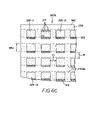
- FIG. 6A depicts schematically a plan view of a cover plate having provided thereon a plurality of unidirectional patterns of a pressure-sensitive adhesive material in accordance with an aspect of the present invention
- FIG. 6B is the same plan view of the device substrate as shown in FIG. 3B ;
- FIG. 6C is a schematic plan view of an aligned and bonded assembly of the device substrate of FIG. 6B and the cover plate of FIG. 6A , and showing uniform bonds provided over and between device display areas by the pressure-sensitive adhesive pattern while keeping electrical interconnect areas free from adhesive material in accordance with aspects of the present invention;
- FIG. 7A is a schematic plan view of a cover plate having provided thereon a plurality of rectangular patterns of a pressure-sensitive adhesive material in accordance with an aspect of the present invention
- FIG. 7B is the same plan view of the device substrate as shown in FIG. 3B ;
- FIG. 8A is a schematic plan view of a cover plate having provided thereon a layer of a pressure-sensitive adhesive material in which a pattern of rectangular cut-outs or openings is arranged;
- FIG. 8B is the same plan view of the device substrate as shown in FIG. 3B ;
- FIG. 9 is a schematic perspective view of a singulated packaged OLED device having a cover plate bonded over the device by a layer of a pressure-sensitive adhesive material in accordance with the present invention, and shown operative to provide light emission from a pixel;
- FIG. 10 is an enlarged sectional view of a pixel of the OLED device of FIG. 9 , and showing an encapsulation layer and an inner portion of an electrical interconnect member.
- the drawings are necessarily of a schematic nature since layer thicknesses are frequently in the sub-micrometer range and pixel dimensions can be in a range of 5–250 micrometer, while lateral dimensions of device substrates and of cover plates can be in a range of 10–50 centimeter. Accordingly, the drawings are scaled for ease of visualization rather than for dimensional accuracy.
- the term “transparent” refers to an encapsulation layer, a layer of a pressure-sensitive adhesive material, a cover plate in a top-emitting OLED device configuration, as well as anode electrode layer(s), and a device substrate in a bottom-emitting OLED device configuration, and denotes an optical transmission of at least 80% of a light directed perpendicularly at a surface of such members.
- the term “optically reflective” refers to a cover plate surface in a bottom-emitting OLED device configuration, and denotes a reflectance greater than 60% of light directed perpendicularly at such surface.
- optical absorptive refers to a cover plate surface in a bottom-emitting OLED device configuration, and denotes an absorption of at least 90% of light directed perpendicularly at such surface.
- pixel is generally used to designate the smallest addressable element of a pixelated OLED display, and denotes herein the light-emitting portion of a pixel.
- FIGS. 1A–1D indicate schematically a process which results in bonding with a layer of a pressure-sensitive adhesive (PSA) material a common cover plate over and between a plurality of OLED devices, which can be encapsulated, formed on a device substrate.
- PSA pressure-sensitive adhesive
- FIG. 1A is a schematic sectional view of a layer 270 of a PSA material disposed between a first release liner 271 and a second release liner 272 .
- Pressure-sensitive adhesive materials disposed between two release liners are commercially available, for example, from 3M Company of (St. Paul, Minn., USA) in the form of a roll which can be cut into sheets of a desired size or area.
- the release liners can be made of a polyester material or of other materials which can be readily peeled off, or released from the adhesive layer 270 .
- the adhesive layer 270 can be formed of an acrylic adhesive material or of other adhesive materials which permit “dry” bonding to a surface or “dry” bonding between two surfaces without a requirement of curing such adhesive bonds.
- FIG. 1B depicts the PSA-layer disposed on the second release liner 272 after peeling or releasing the first release liner 271 .
- FIG. 1C indicates schematically the bonding or transferring of the PSA-layer 270 to a first surface 253 of a cover plate 252 which has an opposing second surface 259 .
- the bonding or transferring is achieved by transporting the cover plate 252 and the PSA-layer 270 (disposed on the second release liner 272 ) through a pressure roller apparatus 700 which is also referred to as a roller laminator.
- a pressure roller apparatus 700 which is also referred to as a roller laminator.
- both rollers of the laminator are driven synchronously by a common drive mechanism and the rotational speed of the rollers can be adjusted to provide a selected speed of transporting the cover plate and the PSA-layer.
- a force F 1 is indicated in FIG. 1C as being directed to each of the rollers of the apparatus 700 .
- one of the rollers can be translated in a vertical direction to provide a selected force or a selected pressure with respect to an opposing second roller which is mounted rigidly in such vertical direction.
- Both pressure rollers of the apparatus 700 can be heated to a temperature in a range of from 40 to 75° C.
- a cover plate configuration 250 is obtained which has an unpatterned layer of a PSA material uniformly bonded over at least a portion of the first cover plate surface 253 .
- the second release liner 272 is now peeled off, or released from, the unpatterned layer of the PSA material 270 .
- FIG. 1D shows schematically the process of uniformly bonding the cover plate 252 via the PSA-layer 270 over and between a plurality of OLED devices provided on a first surface 303 of a device substrate 302 having an opposing second surface 305 .
- the position of a pixelated display area of one of the OLED devices is indicated at 325 - xy .
- a force F 2 or forces F 2 , directed in a vertical direction between the pressure rollers of the pressure roller apparatus 700 , is selected to result in a bonding layer 270 bu of unpatterned PSA material which extends over and between the OLED devices and to provide a bonded assembly configuration 360 bu having an unpatterned layer of a PSA material.
- the pressure rollers of the apparatus are heated to a temperature in a range of from 40 to 75° C. so that uniform bonding can be provided over all topological features of the OLED devices.
- FIG. 2 is a schematic side view of a guiding assembly 702 for guiding the device substrate 302 and the cover plate 252 in lateral registration into a nip region of the roller laminator 700 .
- a device substrate feed table 710 has a feed table surface 712 .
- Fixedly mounted over the surface 712 is a feed guide 720 which includes a feed guide recess 722 for slideably accepting an edge of the device substrate 302 .
- the cover plate 252 bearing the unpatterned layer 270 of the PSA material is guided along a feed guide surface 724 towards the nip region between rollers of the pressure roller apparatus 700 . At least one lateral edge of the device substrate 302 and the cover plate 252 , respectively, are guided by the guiding assembly 702 .
- FIG. 3A is a schematic plan view of a portion of a cover plate configuration 250 which includes an unpatterned layer 270 of a PSA material laminated over a first surface 253 of the cover plate 252 by the method described with reference to FIG. 1C upon peeling the second release liner 272 .
- FIG. 3B is a schematic plan view, a portion of an OLED device configuration 300 which includes a plurality of OLED devices formed in a two-dimensional array on a first surface 303 of a device substrate 302 .
- Each OLED device includes a pixelated display area 325 having picture elements or pixels “pix”, and at least one electrical interconnect area 328 .
- Neighbor OLED devices are separated by a spacing sx along an x-direction and by spacing sy along a y-direction.
- the pixelated structure of an OLED display area is indicated schematically within the display area of only one OLED device.
- the positions of only three pixelated OLED display areas 325 within the two-dimensional array are indicated at 325 - 11 , corresponding to a position 1 ; 1 , 325 - 31 , corresponding to a position 3 ; 1 , and 325 - 14 , corresponding to a position 1 ; 4 along the x-direction and along the y-direction, respectively.
- the pixelated display areas 325 can be those of passive matrix OLED devices, or the pixelated display areas can be associated with active matrix OLED devices.
- the cover plate configuration 250 is bonded over the OLED device configuration 300 by the process described with reference to FIG. 1D and using the guiding assembly 702 shown in FIG. 2 .
- residual adhesive material has to be removed from outermost portions of the electrical interconnect area or areas upon singulating a plurality of packaged OLED devices (see FIG. 9 ). Removing such residual PSA material from the interconnect area(s) can be achieved, for example, by using a conventional adhesive tape. The adhesive portion of the tape is first pressed manually over the electrical interconnect area 328 having the residue of PSA material and is subsequently peeled off, thereby lifting off the residual PSA material from the electrical interconnects.
- the PSA material can be left on the electrical interconnect area and, after singulating the devices, then subsequently removed.
- a release agent can also be used.
- FIG. 4A is a schematic plan view of the same cover plate configuration 250 described above with reference to FIG. 3A .
- FIG. 4B is a schematic plan view of a modified OLED device configuration 300 R in which a thin film of a release agent 400 , depicted in bold dotted outline, is formed over outermost portions of the electrical interconnect areas 328 by a printing process, by a spraying process, by an evaporation process, or by a sputtering process.
- the release agent is selected so that the layer of the PSA material does not bond effectively, or does not bond at all, to the electrical interconnect areas 328 which are coated with such release agent.
- PSA material is released from these outermost portions of the electrical interconnect areas upon singulating the cover plate (see FIG. 9 ).
- the layer of PSA material is bonded strongly to that portion of the cover plate 252 which is singulated to reveal, and to provide electrical access to, the electrical interconnect areas for attaching electrical leads thereto.
- the release agent 400 can be a thin film having a thickness in a range of from a few molecular monolayers to 10 nanometer. Such thin film of a release agent is sufficiently thin and electrically insulative in a lateral direction between laterally adjacent interconnect elements so that electrical leads can be reliably connected to each interconnect element of the electrical interconnect area 328 through the thin film of the release agent 400 .
- Preferred release agent materials include silicone compounds, organo-silicon compounds, and fluorocarbon compounds.
- the cover plate configuration 250 is bonded over the OLED device configuration 300 R by the process described with reference to FIG. 1D and using the guiding assembly 702 shown in FIG. 2 .
- FIGS. 5A–5D show schematically another process sequence which results in bonding with a patterned layer of a PSA material a common cover plate over at least pixelated display areas of a plurality of OLED devices formed on a device substrate.
- FIG. 5A is a schematic sectional view of a repeating pattern formed in the first release liner 271 p and in the PSA-layer 270 p .
- the repeating patterns 271 p and 270 p can be formed by a rotary die cutting process which is a known process in use in manufacturing adhesive labels of various sizes and shapes.
- the second release liner is supported on a rigid support 800 which can be a support having peripheral vacuum grooves for drawing the second release liner against the support in a planar position.
- FIG. 5B reveals the patterned layer 270 p of the PSA material upon peeling or releasing the patterns 271 p of the first release liner.
- FIG. 5C indicates schematically the bonding of the repeating pattern 270 p of the PSA material to a first surface 253 of a cover plate 252 by transporting the second release liner 272 and the cover plate 252 through the pressure roller apparatus or roller laminator 700 , as described above with reference to FIG. 1C .
- a cover plate configuration 250 p is obtained which has a patterned layer of a PSA material bonded over portions of the first cover plate surface 253 .
- the second release liner is now peeled off, or released from, the patterned layer 270 p of the PSA material.
- FIG. 5D shows schematically the process of bonding the cover plate configuration 250 p over at least the display area 325 of each one of the plurality of OLED devices formed on the first surface 303 of the device substrate 302 .
- the bonding is achieved by transporting the cover plate configuration 250 p and the device substrate in lateral alignment through the roller laminator 700 while the rollers are heated to a temperature in a range of from 40 to 75° C.
- a bonding layer 270 bp of a patterned PSA material is obtained which extends at least over the pixelated display areas of each OLED device while leaving electrical interconnect areas free of PSA material (see FIGS. 6A , 6 C, 7 A, and 8 A).
- a bonded and aligned assembly configuration 360 bp results from this process sequence and having the patterned bonding layer 270 bp.
- FIGS. 6A , 6 B, and 6 C are schematic plan views of respectively corresponding cover plate configurations 250 A, 250 B, and 250 C having provided on a first cover plate surface 253 different patterns of a PSA material.
- FIGS. 6B , 7 B, and 8 B are schematic plan views of OLED device configurations 300 which are identical to the device configuration described above with reference to FIG. 3B .
- a unidirectional and laterally spaced pattern of stripes 270 A of a layer of PSA material extends along an x-direction across the first surface 253 of the cover plate.
- Each of the stripes has a width dimension WAy in a y-direction.
- the unidirectional stripe pattern is formed by rotary die cutting as described previously with reference to FIG. 5A , and the pattern of the PSA material is laminated to the cover plate by the process described with reference to FIG. 5C .
- the lateral spacing between adjacent stripes and the width dimension WAy of the stripes is selected to be aligned with respect to the OLED devices on the device substrate 302 so that outermost portions of the electrical interconnect areas 328 remain free of PSA material while at least the display areas 325 of the OLED devices and areas between adjacent display areas along an x-direction receive a bonded cover plate, as indicated by dotted reference lines which extend between FIGS. 6A and 6B .
- the cover plate configuration 250 A is bonded over the OLED device configuration 300 by the process described above with reference to FIG. 5D .
- FIG. 6C is a plan view of the bonded and aligned assembly configuration 360 A in which the cover plate is bonded over the device substrate by the stripe pattern 270 Ab of the PSA material. A common edge 362 of the aligned and bonded cover plate and device substrate is indicated.
- the OLED device configuration 300 of FIG. 6B includes an additional electrical interconnect area (not shown in the drawings) located along an opposing side of the electrical interconnect areas 328 , the width dimension WAy of the stripes of PSA material is selected so that such additional electrical interconnect areas also remain free from PSA material.
- FIG. 7A is a schematic plan view of a cover plate configuration 250 B in which a layer of a PSA material has been patterned to provide a plurality of laterally spaced rectangles or squares 270 B over the first surface 253 of the cover plate 252 .
- Such patterning can be achieved by the rotary die cutting process described with reference to FIG. 5A , and bonding of the patterned layer of PSA material to the cover plate can be accomplished by the process described with reference to FIG. 5C .
- the adhesive pattern is depicted with rectangles having a width dimension WBx along an x-direction and a width dimension WBy along a y-direction.
- Dotted reference lines extending between FIG. 7A and FIG. 7B indicate the positions of bonding the cover plate configuration 250 B in alignment with respect to the OLED devices of the device configuration 300 .
- the patterns 270 B of the layer of PSA material can have width dimensions WBx and WBy which are selected so that bonding of the common cover plate is provided only over the pixelated display area 325 of each OLED device of the device configuration 300 .
- the patterns 270 B can be scaled dimensionally to provide effective cover plate bonding over a plurality of OLED devices which can have electrical interconnect areas extending along four peripheral portions of the pixelated display areas 325 .
- FIG. 8A is a schematic plan view of a cover plate configuration 250 C in which a layer of a PSA material 270 C has been patterned to provide a plurality of cut-outs or openings 275 arranged to align with the electrical interconnect areas 328 of the OLED devices of the device configuration 300 of FIG. 8B as indicated by dotted reference lines extending between FIG. 8A and FIG. 8B . If the OLED devices are formed to have more than the one electrical interconnect area 328 , additional cut-outs or openings can be provided in the PSA-layer in spatial correspondence with the locations of additional electrical interconnect areas.
- FIG. 9 a schematic perspective view is shown of a singulated packaged OLED device 360 As which has been singulated from the assembly configuration 360 A of FIG. 6C , and indicating the bonding layer 270 A of the PSA material.
- the singulated device substrate 302 s and the singulated transparent cover plate 252 s share common singulated dimensions along three edges.
- the singulation of the cover plate is offset laterally with respect to the device substrate along the interconnect area.
- First and second surfaces 303 and 305 , respectively, of the singulated device substrate 302 s are shown. Also indicated is the second surface 259 of the singulated cover plate 252 s.
- the singulated OLED device 360 As is depicted here as an example of a top-emitting device having a singulated transparent cover plate 252 s.
- Light emission 390 from a pixel is directed toward an observer through the transparent cover plate and its second surface 259 .
- Light emission, of any one pixel at an instant of time occurs in response to electrical drive signals and electrical control signals provided at the electrical interconnect area 328 by electrical leads 528 connected thereto.
- Electrical leads 528 are the output leads issuing from an output terminal 510 of a power supply, scan line generator, and signal processor 500 which, in turn, receives an input signal at an input terminal 504 via a signal lead 502 .
- the pixelated display area 325 - xy (and its associated electrical interconnect area 328 ) can be that of any of the OLED devices singulated from the assembly 360 A of FIG. 6C .
- the outermost portions 328 of the electrical interconnect area extend in the form of inner portions 328 i under the bonded cover plate to the display area 325 - xy.
- FIG. 10 is a schematic enlarged view of a pixel “pix” taken along the section lines 10 — 10 of the assembly configuration 360 A of FIG. 9 .
- a device substrate 302 has opposing first and second surfaces 303 and 305 , respectively.
- the pixel includes an anode electrode layer 304 formed on the first surface 303 of the device substrate 302 .
- the anode electrode layer 304 is in electrical contact with a metallized conductor (not identified) which is the inner portion 328 i of the electrical interconnect area 328 .
- An organic EL medium structure is provided over a portion of the anode electrode layer 304
- a cathode electrode layer 306 is provided over a portion of the EL medium structure.
- An electrical interconnect element or elements dedicated to the cathode electrode layer(s) is not shown in this drawing.
- a transparent encapsulation layer 310 fully encapsulates the pixel and inner portions of the electrical interconnects to provide an effective barrier against moisture penetration and oxygen penetration.
- a transparent encapsulation layer 310 can be formed by known thin-film deposition methods such as, for example, thermal vapor deposition, sputter deposition, or atomic layer deposition.
- Materials suitable as encapsulation layer materials include aluminum oxide, silicon nitride, silicon-oxinitride, and tantalum oxide. Due to the thin-film structure of such encapsulation layer, it does not provide adequate mechanical protection. Thus, a bonded cover plate is required to ensure mechanical protection of the OLED devices.
- the bonding layer 270 Ab uniformly bonds the first cover plate surface 253 over all topological features of the pixel, including the spacing 355 between an upper surface of the encapsulation layer 310 and the surface 253 .
- the cathode electrode layer 306 , the encapsulation layer 310 , the bonding layer 270 Ab of the PSA material, and the cover plate 252 have to be transparent elements for the light generated within the EL medium structure.
- a transparent cover plate can be a glass plate, a quartz plate, or a polymer plate such as, for example, a polycarbonate plate.
- the anode electrode layer 304 and the device substrate have to be transparent elements.
- the cover plate can be constructed from an optically opaque material which can be optically reflective or optically absorptive.
- an optically reflective cover plate can take the form of a metal plate having a reflective first surface 253 , a ceramic plate having such reflective surface, a glass plate having a reflective first surface 253 , or a polymer plate having such reflective surface.
- An optically absorptive cover plate can take the form of a polymer cover plate which includes a dye selected to absorb the light generated within the EL medium structure.
- an optically absorptive cover plate can be a transparent cover plate or a ceramic cover plate having deposited on the first surface 253 an absorptive layer.
Abstract
Description
-
- 1) increasing the aperture ratio, therefore permitting pixels of the display to operate at a lower current density which results in improved operational stability;
- 2) permitting more complex drive circuitry to enable improved control of pixel current, leading to enhanced display uniformity and to improved display stability;
- 3) enabling the use of lower mobility materials, e.g. amorphous silicon, to be considered in forming the thin-film transistor (TFT) drive circuitry; and
- 4) permitting incorporation of elements which can increase the out-coupling of light generated within the organic EL medium structure to provide increased efficiency of emitted light.
- 250 cover plate configuration with unpatterned layer of a pressure-sensitive adhesive (PSA) material
- 250 p cover plate configuration with patterned layer of a PSA material
- 250A cover plate configuration with a first pattern of a layer of a PSA material
- 250B cover plate configuration with a second pattern of a layer of a PSA material
- 250C cover plate configuration with a third pattern of a layer of a PSA material
- 252 cover plate
- 252 s singulated cover plate
- 253 first surface of cover plate (252)
- 259 second surface of cover plate (252)
- 270 unpatterned layer of a PSA material
- 270A unidirectional stripe pattern(s) of a layer of PSA material
- 270B rectangular or square pattern(s) of a layer of PSA material
- 270C layer of PSA material with pattern(s) of cut-outs or openings (275)
- 270 bu bonding layer of unpatterned PSA material
- 270 p patterned layer of a PSA material
- 270 bp bonding layer of patterned PSA material
- 270Ab bonding layer of PSA material with stripe pattern (270A)
- 271 first release liner
- 271 p patterned first release liner
- 272 second release liner
- 275 cut-outs or openings formed in layer of PSA material (270 c)
- 300 OLED device configuration with an electrical interconnect area
- 300R OLED device configuration with an electrical interconnect area having a release agent (400)
- 302 device substrate
- 302 s singulated device substrate
- 303 first surface of device substrate (302)
- 304 anode electrode layer
- 305 second surface of device substrate (302)
- 306 cathode electrode layer
- 310 encapsulation layer
- 325 pixelated OLED display area
- 325-11 pixelated OLED display area at a position (1;1)
- 325-14 pixelated OLED display area at a position (1;4)
- 325-31 pixelated OLED display area at a position (3; 1)
- 325-xy pixelated OLED display area at a position (x;y)
- 328 outermost portion(s) of electrical interconnect area(s)
- 328 i inner portion(s) of electrical interconnect area(s)
- 355 spacing between upper surface of encapsulation layer (310) and first surface (253) of cover plate (252)
- 360A bonded and aligned assembly configuration having the stripe pattern (270A) of the layer of PSA material
- 360As singulated packaged OLED device (from assembly configuration 360 a)
- 360 bp bonded and aligned assembly configuration having a patterned layer of a PSA material
- 360 bu bonded assembly configuration having an unpatterned layer of a PSA material
- 362 common edge(s) of aligned and bonded cover plate (252) and device substrate (302)
- 390 light emission from a pixel
- 400 thin film of release agent formed over electrical interconnect areas (328)
- 500 power supply, scan line generator, and signal processor
- 502 signal lead
- 504 input terminal
- 510 output terminal
- 528 electrical leads
- 700 pressure roller apparatus, or roller laminator
- 702 guiding assembly
- 710 device substrate feed table
- 712 feed table surface
- 720 feed guide
- 722 feed guide recess for slideably accepting an edge of the device substrate (302)
- 724 feed guide surface for cover plate (252)
- 800 rigid support
- EL organic electroluminescent (“EL”) medium structure
- F1 force on pressure rollers for laminating layer of PSA material to cover plate surface (253)
- F2 force on pressure rollers for bonding cover plate (252) to device substrate (302)
- pix light-emitting portion of a pixel
- sx spacing between OLED devices along an x-direction
- sy spacing between OLED devices along a y-direction
- WAy width dimension in a y-direction of pattern (270A)
- WBx width dimension in an x-direction of pattern (270B)
- WBy width dimension in a y-direction of pattern (270B)
- x x-direction
- y y-direction
Claims (14)
Priority Applications (1)
| Application Number | Priority Date | Filing Date | Title |
|---|---|---|---|
| US10/787,513 US7135352B2 (en) | 2004-02-26 | 2004-02-26 | Method of fabricating a cover plate bonded over an encapsulated OLEDs |
Applications Claiming Priority (1)
| Application Number | Priority Date | Filing Date | Title |
|---|---|---|---|
| US10/787,513 US7135352B2 (en) | 2004-02-26 | 2004-02-26 | Method of fabricating a cover plate bonded over an encapsulated OLEDs |
Publications (2)
| Publication Number | Publication Date |
|---|---|
| US20050227387A1 US20050227387A1 (en) | 2005-10-13 |
| US7135352B2 true US7135352B2 (en) | 2006-11-14 |
Family
ID=35061061
Family Applications (1)
| Application Number | Title | Priority Date | Filing Date |
|---|---|---|---|
| US10/787,513 Active 2024-10-19 US7135352B2 (en) | 2004-02-26 | 2004-02-26 | Method of fabricating a cover plate bonded over an encapsulated OLEDs |
Country Status (1)
| Country | Link |
|---|---|
| US (1) | US7135352B2 (en) |
Cited By (7)
| Publication number | Priority date | Publication date | Assignee | Title |
|---|---|---|---|---|
| US20090179550A1 (en) * | 2008-01-15 | 2009-07-16 | Samsung Electronics Co., Ltd. | Organic light emitting display device having protecting layers and method of manufacturing the same |
| US20110049547A1 (en) * | 2009-09-02 | 2011-03-03 | Wisepal Technologies, Inc. | Fabricating method and structure of a wafer level module |
| US8236126B2 (en) | 2010-07-14 | 2012-08-07 | Industrial Technology Research Institute | Encapsulation method of environmentally sensitive electronic element |
| US20130068374A1 (en) * | 2011-09-20 | 2013-03-21 | Edward James Balaschak | APPARATUS AND METHOD FOR LARGE AREA HERMETIC ENCAPSULATION OF ONE OR MORE ORGANIC LIGHT EMITTING DIODES (OLEDs) |
| TWI411024B (en) * | 2009-09-02 | 2013-10-01 | Himax Semiconductor Inc | Fabricating method and structure of a wafer level module |
| US20170194594A1 (en) * | 2015-03-02 | 2017-07-06 | Boe Technology Group Co., Ltd. | Packaging assembly and manufacturing method thereof |
| US10326160B2 (en) | 2011-11-18 | 2019-06-18 | Samsung Electronics Co., Ltd. | Cathode and lithium battery using the same |
Families Citing this family (9)
| Publication number | Priority date | Publication date | Assignee | Title |
|---|---|---|---|---|
| KR101147082B1 (en) | 2009-05-20 | 2012-05-17 | 황장환 | Method for Manufacturing Display Device |
| KR101697803B1 (en) * | 2009-06-01 | 2017-01-18 | 스미또모 가가꾸 가부시키가이샤 | Encapsulation process and structure for electronic devices |
| WO2014145200A2 (en) * | 2013-03-15 | 2014-09-18 | Thomas Brindisi | Volumetric three-dimensional display with evenly-spaced elements |
| KR101596725B1 (en) * | 2013-05-22 | 2016-02-24 | 삼성디스플레이 주식회사 | Filling film and manufacturing method of organic light emitting display apparatus using the same |
| US10084135B2 (en) * | 2014-11-27 | 2018-09-25 | Industrial Technology Research Institute | Illumination device and method of fabricating an illumination device |
| US20190207170A1 (en) * | 2016-09-05 | 2019-07-04 | Sharp Kabushiki Kaisha | Transport tool and method for manufacturing organic electroluminescent display device using said transport tool |
| US10452888B2 (en) * | 2016-11-24 | 2019-10-22 | Boe Technology Group Co., Ltd. | Flexible touch panel, flexible display panel and flexible display apparatus, and fabricating method thereof |
| JP6559758B2 (en) * | 2017-12-01 | 2019-08-14 | 住友化学株式会社 | Manufacturing method of electronic device |
| CN110238526B (en) * | 2019-07-17 | 2022-01-18 | 昆山龙腾光电股份有限公司 | Display panel manufacturing method, display panel and welding device |
Citations (10)
| Publication number | Priority date | Publication date | Assignee | Title |
|---|---|---|---|---|
| US5920080A (en) * | 1997-06-23 | 1999-07-06 | Fed Corporation | Emissive display using organic light emitting diodes |
| WO2000026973A1 (en) * | 1998-11-02 | 2000-05-11 | Presstek, Inc. | Transparent conductive oxides for plastic flat panel displays |
| US6268695B1 (en) | 1998-12-16 | 2001-07-31 | Battelle Memorial Institute | Environmental barrier material for organic light emitting device and method of making |
| WO2002005361A1 (en) * | 2000-07-12 | 2002-01-17 | 3M Innovative Properties Company | Encapsulated organic electronic devices and method for making same |
| US20030143423A1 (en) * | 2002-01-31 | 2003-07-31 | 3M Innovative Properties Company | Encapsulation of organic electronic devices using adsorbent loaded adhesives |
| US20030205317A1 (en) | 2002-05-01 | 2003-11-06 | Ha Chau Thi Minh | Method for sealing flat panel displays and bonding optical component parts |
| EP1361556A1 (en) | 2001-01-24 | 2003-11-12 | Sony Corporation | Display device |
| US6835950B2 (en) * | 2002-04-12 | 2004-12-28 | Universal Display Corporation | Organic electronic devices with pressure sensitive adhesive layer |
| US20050045900A1 (en) * | 2003-08-25 | 2005-03-03 | Universal Display Corporation | Protected organic electronic device structures incorporating pressure sensitive adhesive and desiccant |
| US6897474B2 (en) * | 2002-04-12 | 2005-05-24 | Universal Display Corporation | Protected organic electronic devices and methods for making the same |
-
2004
- 2004-02-26 US US10/787,513 patent/US7135352B2/en active Active
Patent Citations (11)
| Publication number | Priority date | Publication date | Assignee | Title |
|---|---|---|---|---|
| US5920080A (en) * | 1997-06-23 | 1999-07-06 | Fed Corporation | Emissive display using organic light emitting diodes |
| WO2000026973A1 (en) * | 1998-11-02 | 2000-05-11 | Presstek, Inc. | Transparent conductive oxides for plastic flat panel displays |
| US6268695B1 (en) | 1998-12-16 | 2001-07-31 | Battelle Memorial Institute | Environmental barrier material for organic light emitting device and method of making |
| WO2002005361A1 (en) * | 2000-07-12 | 2002-01-17 | 3M Innovative Properties Company | Encapsulated organic electronic devices and method for making same |
| US6867539B1 (en) * | 2000-07-12 | 2005-03-15 | 3M Innovative Properties Company | Encapsulated organic electronic devices and method for making same |
| EP1361556A1 (en) | 2001-01-24 | 2003-11-12 | Sony Corporation | Display device |
| US20030143423A1 (en) * | 2002-01-31 | 2003-07-31 | 3M Innovative Properties Company | Encapsulation of organic electronic devices using adsorbent loaded adhesives |
| US6835950B2 (en) * | 2002-04-12 | 2004-12-28 | Universal Display Corporation | Organic electronic devices with pressure sensitive adhesive layer |
| US6897474B2 (en) * | 2002-04-12 | 2005-05-24 | Universal Display Corporation | Protected organic electronic devices and methods for making the same |
| US20030205317A1 (en) | 2002-05-01 | 2003-11-06 | Ha Chau Thi Minh | Method for sealing flat panel displays and bonding optical component parts |
| US20050045900A1 (en) * | 2003-08-25 | 2005-03-03 | Universal Display Corporation | Protected organic electronic device structures incorporating pressure sensitive adhesive and desiccant |
Non-Patent Citations (2)
| Title |
|---|
| Craig Adhesives and Coatings Company, UV Pressure Sensitive Adhesives,□□http://www.craigahesives.com/UV/Laminating.htm; and Products,□□http://www/craogadhesives.com/products.htm. * |
| Silvernail, J. et al., "Packaging OLED Displays Using Dual Stage Pressure Sensitive Adhesives", 15 page Pwer Point Presentation, presented on Oct. 11, 2002. * |
Cited By (11)
| Publication number | Priority date | Publication date | Assignee | Title |
|---|---|---|---|---|
| US20090179550A1 (en) * | 2008-01-15 | 2009-07-16 | Samsung Electronics Co., Ltd. | Organic light emitting display device having protecting layers and method of manufacturing the same |
| US20110049547A1 (en) * | 2009-09-02 | 2011-03-03 | Wisepal Technologies, Inc. | Fabricating method and structure of a wafer level module |
| US8193599B2 (en) * | 2009-09-02 | 2012-06-05 | Himax Semiconductor, Inc. | Fabricating method and structure of a wafer level module |
| TWI411024B (en) * | 2009-09-02 | 2013-10-01 | Himax Semiconductor Inc | Fabricating method and structure of a wafer level module |
| US8236126B2 (en) | 2010-07-14 | 2012-08-07 | Industrial Technology Research Institute | Encapsulation method of environmentally sensitive electronic element |
| US20130068374A1 (en) * | 2011-09-20 | 2013-03-21 | Edward James Balaschak | APPARATUS AND METHOD FOR LARGE AREA HERMETIC ENCAPSULATION OF ONE OR MORE ORGANIC LIGHT EMITTING DIODES (OLEDs) |
| US8936690B2 (en) * | 2011-09-20 | 2015-01-20 | General Electric Company | Apparatus and method for large area hermetic encapsulation of one or more organic light emitting diodes (OLEDs) |
| TWI567850B (en) * | 2011-09-20 | 2017-01-21 | 京東方科技集團股份有限公司 | Apparatus and method for large area hermetic encapsulation of one or more organic light emitting diodes (oleds) |
| US10326160B2 (en) | 2011-11-18 | 2019-06-18 | Samsung Electronics Co., Ltd. | Cathode and lithium battery using the same |
| US20170194594A1 (en) * | 2015-03-02 | 2017-07-06 | Boe Technology Group Co., Ltd. | Packaging assembly and manufacturing method thereof |
| US10326105B2 (en) * | 2015-03-02 | 2019-06-18 | Boe Technoogy Group Co., Ltd. | Packaging assembly and manufacturing method thereof |
Also Published As
| Publication number | Publication date |
|---|---|
| US20050227387A1 (en) | 2005-10-13 |
Similar Documents
| Publication | Publication Date | Title |
|---|---|---|
| US7279063B2 (en) | Method of making an OLED display device with enhanced optical and mechanical properties | |
| US7135352B2 (en) | Method of fabricating a cover plate bonded over an encapsulated OLEDs | |
| CN100595931C (en) | Electroluminescent display device and thermal transfer donor film for the electroluminescent display device | |
| KR100983446B1 (en) | Organic electroluminescent device, fabrication method and forming method thereof | |
| US7301277B2 (en) | Electro-optical apparatus, manufacturing method thereof, and electronic instrument | |
| KR101717472B1 (en) | Laminate for encapsulation, organic light emitting apparatus and manufacturing methode thereof | |
| KR100941129B1 (en) | Light emitting device and method of manufacturing the same | |
| US20070194303A1 (en) | Method for manufacturing organic light-emitting element, organic light-emitting device and organic EL panel | |
| US11011728B2 (en) | Display device | |
| US8912018B2 (en) | Manufacturing flexible organic electronic devices | |
| US7932670B2 (en) | Organic electro-luminescence display device and method of manufacturing the same | |
| US20030042852A1 (en) | Encapsulation structure, method, and apparatus for organic light-emitting diodes | |
| US7248309B2 (en) | Liquid crystal display device and method for fabricating the same | |
| KR20150042367A (en) | Organic electro luminescent device and method of fabricating the same | |
| JP5750119B2 (en) | Optoelectronic device array | |
| JP2004342432A (en) | Organic el (electroluminescence) display device | |
| US20090200924A1 (en) | Oganic EL display device and manufacturing method thereof | |
| US20050140260A1 (en) | Organic electroluminescent device having supporting plate and method of fabricating the same | |
| TW201405909A (en) | Light emitting device, display unit including the same, and electronic apparatus | |
| KR20080090945A (en) | Organic light emitting display apparatus | |
| TW201024836A (en) | Display drivers | |
| JP2010020973A (en) | Manufacturing method of organic el display device | |
| JP2002050471A (en) | Organic electroluminescence element and its manufacturing method | |
| US8152583B2 (en) | Manufacturing method of organic EL display device | |
| KR101993287B1 (en) | Organic light emitting display device and method of fabricating thereof |
Legal Events
| Date | Code | Title | Description |
|---|---|---|---|
| AS | Assignment |
Owner name: EASTMAN KODAK COMPANY, NEW YORK Free format text: ASSIGNMENT OF ASSIGNORS INTEREST;ASSIGNORS:YOKAJTY, JOSEPH E.;SERBICKI, JEFFREY P.;VAN SLYKE, STEVEN A.;REEL/FRAME:015032/0803;SIGNING DATES FROM 20040217 TO 20040224 |
|
| FEPP | Fee payment procedure |
Free format text: PAYOR NUMBER ASSIGNED (ORIGINAL EVENT CODE: ASPN); ENTITY STATUS OF PATENT OWNER: LARGE ENTITY |
|
| STCF | Information on status: patent grant |
Free format text: PATENTED CASE |
|
| CC | Certificate of correction | ||
| FEPP | Fee payment procedure |
Free format text: PAYER NUMBER DE-ASSIGNED (ORIGINAL EVENT CODE: RMPN); ENTITY STATUS OF PATENT OWNER: LARGE ENTITY Free format text: PAYOR NUMBER ASSIGNED (ORIGINAL EVENT CODE: ASPN); ENTITY STATUS OF PATENT OWNER: LARGE ENTITY |
|
| AS | Assignment |
Owner name: GLOBAL OLED TECHNOLOGY LLC,DELAWARE Free format text: ASSIGNMENT OF ASSIGNORS INTEREST;ASSIGNOR:EASTMAN KODAK COMPANY;REEL/FRAME:023998/0368 Effective date: 20100122 Owner name: GLOBAL OLED TECHNOLOGY LLC, DELAWARE Free format text: ASSIGNMENT OF ASSIGNORS INTEREST;ASSIGNOR:EASTMAN KODAK COMPANY;REEL/FRAME:023998/0368 Effective date: 20100122 |
|
| FPAY | Fee payment |
Year of fee payment: 4 |
|
| FPAY | Fee payment |
Year of fee payment: 8 |
|
| MAFP | Maintenance fee payment |
Free format text: PAYMENT OF MAINTENANCE FEE, 12TH YEAR, LARGE ENTITY (ORIGINAL EVENT CODE: M1553) Year of fee payment: 12 |