US7108517B2 - Multi-site chip carrier and method - Google Patents
Multi-site chip carrier and method Download PDFInfo
- Publication number
- US7108517B2 US7108517B2 US10/952,644 US95264404A US7108517B2 US 7108517 B2 US7108517 B2 US 7108517B2 US 95264404 A US95264404 A US 95264404A US 7108517 B2 US7108517 B2 US 7108517B2
- Authority
- US
- United States
- Prior art keywords
- packages
- package
- lid
- recesses
- pressure
- Prior art date
- Legal status (The legal status is an assumption and is not a legal conclusion. Google has not performed a legal analysis and makes no representation as to the accuracy of the status listed.)
- Expired - Fee Related, expires
Links
Images


Classifications
-
- G—PHYSICS
- G01—MEASURING; TESTING
- G01R—MEASURING ELECTRIC VARIABLES; MEASURING MAGNETIC VARIABLES
- G01R1/00—Details of instruments or arrangements of the types included in groups G01R5/00 - G01R13/00 and G01R31/00
- G01R1/02—General constructional details
- G01R1/04—Housings; Supporting members; Arrangements of terminals
- G01R1/0408—Test fixtures or contact fields; Connectors or connecting adaptors; Test clips; Test sockets
- G01R1/0433—Sockets for IC's or transistors
- G01R1/0441—Details
- G01R1/0466—Details concerning contact pieces or mechanical details, e.g. hinges or cams; Shielding
Definitions
- This invention relates to integrated circuit socket devices.
- Integrated circuit (IC) packages must be tested after their manufacture. Testing can include burn-in, testing and programming of IC packages. The integrated circuits are temporarily installed on a circuit board, tested, and then removed from the circuit board. Accordingly, sockets are necessary to install the IC packages on the printed circuit board for testing. These sockets include multiple contacts to connect each of the terminals of the IC package to corresponding conductors on the printed circuit board. Currently, each IC package is tested in a separate socket requiring a test operator to open and close each socket each time an IC is tested. An example of such a socket is the Wells-CTI socket series number 654.
- the sockets are positioned on a printed circuit board where the sockets are arranged in a relatively dense array to allow for as many IC packages as possible to be tested at once. These sockets are therefore arranged in a relatively close side-by-side and end-to-end spacing. However, the number of IC packages tested on a single board is limited to the number of sockets that can fit on the printed circuit board.
- FIG. 1 is a perspective view of an IC package socket device according to the invention shown in an open position.
- FIG. 2 is a perspective view of the IC package socket device of FIG. 1 shown in a closed position.
- FIG. 3 is a cross-sectional view of the IC package socket device of FIG. 1 taken along line 3 — 3 in FIG. 1 showing the device in a fully open-position.
- FIG. 4 is a cross-sectional view of the IC package socket device of FIG. 1 taken along line 3 — 3 in FIG. 1 showing the device in a partially closed position.
- FIG. 5 is a cross-sectional view of the IC package socket device of FIG. 1 taken along line 5 — 5 in FIG. 2 showing the device in a fully closed and latched position.
- FIG. 6 is a detailed perspective view of the lid of the socket device of FIG. 1 showing the multi-site pressure unit.
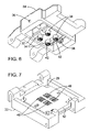
- FIG. 7 is a detailed perspective view of the base of the socket device of FIG. 1 with the lid and latch removed.
- FIGS. 1 and 2 are perspective views of the preferred embodiment of the IC package socket device 20 according to the invention in opened and closed positions, respectively.
- the IC package socket device has a base 22 and a lid 24 that is latched closed onto the base 22 by a latch 26 .
- IC package receiver area 28 in the base 22 receives multiple IC packages 30 (shown in FIGS. 4 and 5 ).
- the receiver area 28 is arranged with an array of recesses 48 to receive two or more (e.g., four) IC packages 30 .
- the socket device can be arranged to receive a die or a packaged die and the term IC package hereinafter will encompass either option.
- the socket device can also be arranged to receive more than one type or size of IC package thereby increasing the versatility and usefulness of the socket device.
- the lid 24 is attached to the base 22 through hinge 50 .
- the latch 26 is positioned opposite hinge 50 .
- a multi-site pressure unit 32 is positioned within the lid 24 in alignment, when closed, with the recesses 48 .
- the pressure unit 32 applies a resilient normal force to the IC packages 30 when the lid 24 is in the closed and latched position shown in FIG. 2 .
- the multi-site pressure unit 32 includes the pressure unit housing 33 and individual pressure pads 34 .
- the cylindrically shaped pressure pads 34 act as plungers and individually apply a resilient normal force to each of the IC packages 30 in recesses 48 .
- the pressure pads 34 could also be otherwise shaped, such as rectangularly or triangularly.
- a textured contact surface 42 of the pressure pad 34 prevents the pressure pad 34 from slipping on the IC package 30 as the lid 24 is closed, thereby helping to maintain substantially equal normal forces across all of the IC packages 30 in the device 20 . Additionally, texturing the contact surfaces of the pressure pads 34 prevents the pads from developing an adhesive suction force on the IC packages 30 .
- the multi-site pressure unit 32 is mounted in the lid 24 on transverse pivot pin 36 .
- the pivot pin 36 allows the pressure unit 32 to rotate as the lid 24 is closed and the pressure pads 34 contact the IC packages 30 .
- the pivot pin 36 is attached to the lid 24 and the pressure unit 32 rocks around the pivot pin 36 .
- a torsional pivot pin spring 38 located on the pivot pin 36 biases the position of the pressure unit 32 so that the pressure pads 34 lie flat on the IC packages 30 when the device 20 is in a closed and latched position.
- FIG. 3 is a cross-sectional view of the IC package socket device in FIG. 1 taken along line 3 — 3 in FIG. 1 .
- the IC package receiver area 28 has a floating plate 52 positioned on floating plate compression springs 46 .
- the floating plate 52 has multiple recesses 48 sized and shaped for receiving individual IC packages 30 , one in each recess 48 .
- the pressure pads 34 are positioned within the multi-site pressure unit 32 so as to align squarely with the array of recesses 48 in floating plate 52 . (See FIGS. 4 and 5 )
- Compression springs 40 are positioned above pressure pads 34 within cylindrical holes in the pressure unit housing 32 .
- the pressure unit 32 attaches to lid 24 by means of the transverse pivot pin 36 .
- the lid 24 is connected to the base 22 by means of hinge 50 .
- Latch 26 is positioned opposite hinge 50 on the base 22 to provide a closing mechanism for the IC package socket device 20 .
- FIG. 4 is a cross-sectional view of the IC package socket device of FIG. 1 showing the device in a partially closed position.
- the pressure pads 34 contact the IC packages 30 with the textured contact surface 42 .
- the pressure unit 32 is tiltably mounted within the lid 24 on transverse pivot pin 36 , the pressure unit rocks so that the pressure pads lie flat on the IC packages 30 as the lid 24 is closed.
- the floating plate compression springs 46 also allow the floating plate 52 to slant, further helping the IC packages 30 lie flat against the pressure pads 34 .
- the torsional spring 38 provides resilient resistance to the rotational motion of the pressure unit 32 .
- the floating plate compression springs 46 also provide resilient resistance to the force of the closing lid on the IC packages 30 . The combination of resilient forces uniformly applied prevents the socket device 20 from damaging the IC packages 30 during the lid closing process.
- FIG. 5 is a cross-sectional view of the IC package socket device of FIG. 1 showing the device in a fully closed and latched position.
- each pressure pad 34 applies a resilient normal force to each IC package 30 .
- the compression springs 40 positioned in the pressure unit 32 above each pressure pad 34 provide the resilient force.
- the resilient normal force applied by the pressure pad 34 and compression spring 40 is sufficient to press each IC package 30 into electrical connection with the electrical contacts 54 in the socket device 20 .
- the device 20 imparts an equal force to each IC package 30 . Minor variations in IC package thicknesses are accommodated through the use of separate pressure pads for each IC package.
- FIG. 6 is a detailed perspective view of the lid 24 of the IC package socket device of FIG. 1 .
- Transverse pivot pin 36 is mounted within the lid 24 and the multi-site pressure unit 32 is rotatably mounted on the transverse pivot pin 36 .
- the torsional spring 38 biases the rotational position of the pressure unit and provides a resilient resistance to rocking motion of the pressure unit 32 .
- Pressure pads 34 with textured contact surfaces 42 are arranged in an array in the pressure unit 32 . While FIG. 6 shows a 2 ⁇ 2 array that accommodates four IC packages, a 1 ⁇ 2 array accommodating two IC packages could be used.
- the array is preferably arranged such that the number of rows equals the number of columns, such as the 2 ⁇ 2 array shown in FIG. 6 .
- the invention anticipates larger arrays including, but not limited to, a 3 ⁇ 3 array accommodating nine ICs or a 4 ⁇ 4 array accommodating sixteen ICs.
- a symmetrical arrangement more easily equally distributes the force of the pressure pads 34 across all of the multiple IC packages.
- the arrangement of pressure pads is not limited to rectangular arrays. Arrangements including circular, hexagonal or triangular arrangements could also be used.
- FIG. 7 is a detailed perspective view of the base 22 of the IC package socket device of FIG. 1 shown with the latch 26 and lid 24 removed.
- the floating plate 52 is positioned within the IC package receiving area 28 .
- the floating plate 52 has an array of recesses 48 sized and shaped for receiving IC packages 30 .
- the recesses 48 can also be shaped and sized separately to receive two or more types or sizes of IC packages within the single socket device 20 .
- the lengths of the pressure pads and the compression springs can be changed as needed to accommodate different thicknesses of IC packages.
- Operation of the IC package socket device includes placing a plurality of IC packages 30 into a single IC package socket device 20 , one in each recess 48 , and applying a separate resilient normal force to each IC package 30 by a plurality of pressure pads 34 positioned within the lid 24 of the testing device 20 .
- the resilient normal force is applied when the lid 24 is closed and latched into place by latch 26 .
- the operation can further include placing a plurality of types or sizes of IC packages into a single package socket device 20 .
- the multi-site socket reduces the amount of time spent burning in, testing and programming IC packages, thereby reducing the cost of manufacturing the IC packages.
Abstract
Description
Claims (28)
Priority Applications (2)
| Application Number | Priority Date | Filing Date | Title |
|---|---|---|---|
| US10/952,644 US7108517B2 (en) | 2004-09-27 | 2004-09-27 | Multi-site chip carrier and method |
| PCT/US2005/034431 WO2006036894A1 (en) | 2004-09-27 | 2005-09-27 | Multi-site chip carrier and method |
Applications Claiming Priority (1)
| Application Number | Priority Date | Filing Date | Title |
|---|---|---|---|
| US10/952,644 US7108517B2 (en) | 2004-09-27 | 2004-09-27 | Multi-site chip carrier and method |
Publications (2)
| Publication Number | Publication Date |
|---|---|
| US20060068614A1 US20060068614A1 (en) | 2006-03-30 |
| US7108517B2 true US7108517B2 (en) | 2006-09-19 |
Family
ID=36099799
Family Applications (1)
| Application Number | Title | Priority Date | Filing Date |
|---|---|---|---|
| US10/952,644 Expired - Fee Related US7108517B2 (en) | 2004-09-27 | 2004-09-27 | Multi-site chip carrier and method |
Country Status (2)
| Country | Link |
|---|---|
| US (1) | US7108517B2 (en) |
| WO (1) | WO2006036894A1 (en) |
Cited By (10)
| Publication number | Priority date | Publication date | Assignee | Title |
|---|---|---|---|---|
| US20070257688A1 (en) * | 2006-05-03 | 2007-11-08 | Micron Technology, Inc. | Systems configured for utilizing two or more of multiple different semiconductor component configurations, methods of providing semiconductor components within sockets, and methods of retaining semiconductor component configurations within sockets |
| US20080020623A1 (en) * | 2006-07-21 | 2008-01-24 | Protos Electronics | Test socket-lid assembly |
| US20080265918A1 (en) * | 2007-04-24 | 2008-10-30 | Protos Electronics, Inc. | Object-clamping lid subassembly of a test socket for testing electrical characteristics of an object |
| US7914313B1 (en) | 2010-02-04 | 2011-03-29 | Plastronics Socket Partners, Ltd. | Clamping mechanism for an IC socket |
| US20120161036A1 (en) * | 2010-12-27 | 2012-06-28 | Hon Hai Precision Industry Co., Ltd. | Testing device for ambient light sensor |
| US8937482B1 (en) | 2011-06-28 | 2015-01-20 | Sensata Technologies, Inc. | Apparatus and method for ramping and controlling the temperature of a component using a vortex tube |
| US10588234B2 (en) | 2016-01-26 | 2020-03-10 | Hewlett Packard Enterprise Development Lp | Semiconductor assembly |
| US20220065921A1 (en) * | 2017-03-03 | 2022-03-03 | Aehr Test Systems | Electronics tester |
| US11592465B2 (en) | 2009-03-25 | 2023-02-28 | Aehr Test Systems | Pressure relief valve |
| US11860221B2 (en) | 2005-04-27 | 2024-01-02 | Aehr Test Systems | Apparatus for testing electronic devices |
Families Citing this family (12)
| Publication number | Priority date | Publication date | Assignee | Title |
|---|---|---|---|---|
| US7955892B2 (en) * | 2007-11-25 | 2011-06-07 | Globalfoundries Inc. | Multiple size package socket |
| TWI450455B (en) * | 2012-06-25 | 2014-08-21 | Hon Hai Prec Ind Co Ltd | Electrical connector |
| TWI448020B (en) * | 2013-05-03 | 2014-08-01 | Hon Hai Prec Ind Co Ltd | Cpu carrier and carrier assembly thereof |
| EP2963430B1 (en) * | 2014-07-03 | 2019-10-02 | Rasco GmbH | Contactor arrangement, test-in-strip handler and test-in-strip handler arrangement |
| WO2019084318A1 (en) * | 2017-10-26 | 2019-05-02 | Xilinx, Inc. | Balanced conforming force mechanism for integrated circuit package workpress testing systems |
| US10564212B2 (en) | 2017-11-02 | 2020-02-18 | Xilinx, Inc. | Integrated circuit package testing system |
| JP7281250B2 (en) * | 2018-05-11 | 2023-05-25 | 株式会社アドバンテスト | test carrier |
| KR102566041B1 (en) * | 2019-11-05 | 2023-08-16 | 주식회사 프로웰 | Semiconductor element test device |
| KR102075484B1 (en) * | 2019-12-30 | 2020-02-10 | 윤찬 | Socket for testing semiconductor |
| KR20230045181A (en) * | 2021-09-28 | 2023-04-04 | 삼성전자주식회사 | Test socket |
| CN114122770B (en) * | 2021-11-25 | 2023-11-28 | 武汉烽唐科技有限公司 | Chip connector |
| DE102022203179B3 (en) | 2022-03-31 | 2023-08-10 | Yamaichi Electronics Deutschland Gmbh | Test contactor with inclinable pressure element |
Citations (6)
| Publication number | Priority date | Publication date | Assignee | Title |
|---|---|---|---|---|
| US5528466A (en) * | 1991-11-12 | 1996-06-18 | Sunright Limited | Assembly for mounting and cooling a plurality of integrated circuit chips using elastomeric connectors and a lid |
| US5648893A (en) * | 1993-07-30 | 1997-07-15 | Sun Microsystems, Inc. | Upgradable multi-chip module |
| US6203332B1 (en) * | 1998-12-22 | 2001-03-20 | Fujitsu Limited | Attachment structure of semiconductor device socket |
| US6464513B1 (en) * | 2000-01-05 | 2002-10-15 | Micron Technology, Inc. | Adapter for non-permanently connecting integrated circuit devices to multi-chip modules and method of using same |
| US6665929B1 (en) * | 2000-01-21 | 2003-12-23 | Cypress Semiconductor Corp. | Method for transferring a plurality of integrated circuit devices into and/or out of a plurality of sockets |
| US6956392B2 (en) * | 2003-12-30 | 2005-10-18 | Texas Instruments Incorporated | Heat transfer apparatus for burn-in board |
-
2004
- 2004-09-27 US US10/952,644 patent/US7108517B2/en not_active Expired - Fee Related
-
2005
- 2005-09-27 WO PCT/US2005/034431 patent/WO2006036894A1/en active Application Filing
Patent Citations (6)
| Publication number | Priority date | Publication date | Assignee | Title |
|---|---|---|---|---|
| US5528466A (en) * | 1991-11-12 | 1996-06-18 | Sunright Limited | Assembly for mounting and cooling a plurality of integrated circuit chips using elastomeric connectors and a lid |
| US5648893A (en) * | 1993-07-30 | 1997-07-15 | Sun Microsystems, Inc. | Upgradable multi-chip module |
| US6203332B1 (en) * | 1998-12-22 | 2001-03-20 | Fujitsu Limited | Attachment structure of semiconductor device socket |
| US6464513B1 (en) * | 2000-01-05 | 2002-10-15 | Micron Technology, Inc. | Adapter for non-permanently connecting integrated circuit devices to multi-chip modules and method of using same |
| US6665929B1 (en) * | 2000-01-21 | 2003-12-23 | Cypress Semiconductor Corp. | Method for transferring a plurality of integrated circuit devices into and/or out of a plurality of sockets |
| US6956392B2 (en) * | 2003-12-30 | 2005-10-18 | Texas Instruments Incorporated | Heat transfer apparatus for burn-in board |
Non-Patent Citations (1)
| Title |
|---|
| Wells-CTI, Technical Drawing entitled "15x15 27mm 1.5mm Pitch Solder Grid Array Socket," Part No. 654XXX227XX0901, Revision C1. |
Cited By (22)
| Publication number | Priority date | Publication date | Assignee | Title |
|---|---|---|---|---|
| US11860221B2 (en) | 2005-04-27 | 2024-01-02 | Aehr Test Systems | Apparatus for testing electronic devices |
| US20090000116A1 (en) * | 2006-05-03 | 2009-01-01 | Cram Daniel P | Methods of Providing Semiconductor Components within Sockets |
| US20080088329A1 (en) * | 2006-05-03 | 2008-04-17 | Cram Daniel P | Systems Configured for Utilizing Two or More Multiple Different Semiconductor Components Configurations, Methods of Providing Semicondutor Components within Sockets, and Methods of Retaining Semiconductor Component Configurations within Sockets |
| US7439752B2 (en) * | 2006-05-03 | 2008-10-21 | Micron Technology, Inc. | Methods of providing semiconductor components within sockets |
| US20070257688A1 (en) * | 2006-05-03 | 2007-11-08 | Micron Technology, Inc. | Systems configured for utilizing two or more of multiple different semiconductor component configurations, methods of providing semiconductor components within sockets, and methods of retaining semiconductor component configurations within sockets |
| US8074353B2 (en) | 2006-05-03 | 2011-12-13 | Micron Technology, Inc. | Methods of providing semiconductor components within sockets |
| US20090009202A1 (en) * | 2006-05-03 | 2009-01-08 | Cram Daniel P | Methods of Retaining Semiconductor Component Configurations within Sockets |
| US20090007423A1 (en) * | 2006-05-03 | 2009-01-08 | Cram Daniel P | Methods of Providing Semiconductor Components within Sockets |
| US7514945B2 (en) | 2006-05-03 | 2009-04-07 | Micron Technology, Inc. | Systems configured for utilizing semiconductor components |
| US7586319B2 (en) | 2006-05-03 | 2009-09-08 | Micron Technology, Inc. | Methods of retaining semiconductor component configurations within sockets |
| US8011092B2 (en) | 2006-05-03 | 2011-09-06 | Micron Technology, Inc. | Methods of providing semiconductor components within sockets |
| US7338295B2 (en) * | 2006-07-21 | 2008-03-04 | Protos Electronics | Test socket-lid assembly |
| US20080020623A1 (en) * | 2006-07-21 | 2008-01-24 | Protos Electronics | Test socket-lid assembly |
| US20080265918A1 (en) * | 2007-04-24 | 2008-10-30 | Protos Electronics, Inc. | Object-clamping lid subassembly of a test socket for testing electrical characteristics of an object |
| US11592465B2 (en) | 2009-03-25 | 2023-02-28 | Aehr Test Systems | Pressure relief valve |
| US7914313B1 (en) | 2010-02-04 | 2011-03-29 | Plastronics Socket Partners, Ltd. | Clamping mechanism for an IC socket |
| US20120161036A1 (en) * | 2010-12-27 | 2012-06-28 | Hon Hai Precision Industry Co., Ltd. | Testing device for ambient light sensor |
| US8937482B1 (en) | 2011-06-28 | 2015-01-20 | Sensata Technologies, Inc. | Apparatus and method for ramping and controlling the temperature of a component using a vortex tube |
| US10588234B2 (en) | 2016-01-26 | 2020-03-10 | Hewlett Packard Enterprise Development Lp | Semiconductor assembly |
| US20220065921A1 (en) * | 2017-03-03 | 2022-03-03 | Aehr Test Systems | Electronics tester |
| US11635459B2 (en) * | 2017-03-03 | 2023-04-25 | Aehr Test Systems | Electronics tester |
| US11821940B2 (en) | 2017-03-03 | 2023-11-21 | Aehr Test Systems | Electronics tester |
Also Published As
| Publication number | Publication date |
|---|---|
| WO2006036894A1 (en) | 2006-04-06 |
| US20060068614A1 (en) | 2006-03-30 |
Similar Documents
| Publication | Publication Date | Title |
|---|---|---|
| US7108517B2 (en) | Multi-site chip carrier and method | |
| EP1116423B1 (en) | Vertically actuated bga socket | |
| US4232928A (en) | Apparatus employing flexible diaphragm for effecting substantially uniform force, individual couplings with multiple electrical contacts or the like | |
| EP1907868B1 (en) | Integrated circuit test socket | |
| EP0746772B1 (en) | Reusable die carrier for burn-in and burn-in process | |
| US9494616B2 (en) | Socket device for testing semiconductor device | |
| US7737710B2 (en) | Socket, and test apparatus and method using the socket | |
| US5376010A (en) | Burn-in socket | |
| US6981882B1 (en) | Packaged device adapter with torque limiting assembly | |
| US7988500B2 (en) | Socket and contact having anchors | |
| WO1999023502A1 (en) | System to simultaneously test trays of integrated circuit packages | |
| US7030638B2 (en) | Method and device with variable resilience springs for testing integrated circuit packages | |
| US20030179009A1 (en) | Compliant actuator for IC test fixtures | |
| US7385408B1 (en) | Apparatus and method for testing integrated circuit devices having contacts on multiple surfaces | |
| US6792375B2 (en) | Apparatus, system, and method of determining loading characteristics on an integrated circuit module | |
| US8981804B2 (en) | Contact apparatus and semiconductor test equipment using the same | |
| US20060051995A1 (en) | Modular semiconductor package testing contactor system | |
| US6765397B2 (en) | Apparatus and method for testing land grid array modules | |
| US6929486B2 (en) | Socket for electrical parts and method for using the same | |
| KR100819836B1 (en) | Carrier module, test handler using the same, and method of manufacturing semiconductor using the same | |
| US8026516B2 (en) | Carrier module for use in a handler and handler for handling packaged chips for a test using the carrier modules | |
| EP0990163A1 (en) | Reusable die carrier for burn-in and burn-in process | |
| US20020043984A1 (en) | Support carrier for temporarily attaching integrated circuit chips to a chip carrier and method | |
| KR100493057B1 (en) | Socket for testing semiconductor chip package available for BGA and TSOP type packages | |
| KR20050009066A (en) | Carrier Module for Semiconductor Test Handler |
Legal Events
| Date | Code | Title | Description |
|---|---|---|---|
| AS | Assignment |
Owner name: WELLS-CTI, LLC, WASHINGTON Free format text: ASSIGNMENT OF ASSIGNORS INTEREST;ASSIGNOR:HARPER, PATRICK HENRY;REEL/FRAME:015439/0043 Effective date: 20040921 |
|
| FEPP | Fee payment procedure |
Free format text: PAYOR NUMBER ASSIGNED (ORIGINAL EVENT CODE: ASPN); ENTITY STATUS OF PATENT OWNER: SMALL ENTITY |
|
| AS | Assignment |
Owner name: SILICON VALLEY BANK, CALIFORNIA Free format text: SECURITY AGREEMENT;ASSIGNOR:WELLS-CTI, LLC;REEL/FRAME:018420/0121 Effective date: 20060901 |
|
| REMI | Maintenance fee reminder mailed | ||
| LAPS | Lapse for failure to pay maintenance fees | ||
| STCH | Information on status: patent discontinuation |
Free format text: PATENT EXPIRED DUE TO NONPAYMENT OF MAINTENANCE FEES UNDER 37 CFR 1.362 |
|
| FP | Lapsed due to failure to pay maintenance fee |
Effective date: 20100919 |
|
| AS | Assignment |
Owner name: WELLS-CTI LLC, WASHINGTON Free format text: RELEASE BY SECURED PARTY;ASSIGNOR:SILICON VALLEY BANK;REEL/FRAME:029430/0786 Effective date: 20121127 |