US7106938B2 - Self assembled three-dimensional photonic crystal - Google Patents
Self assembled three-dimensional photonic crystal Download PDFInfo
- Publication number
- US7106938B2 US7106938B2 US10/801,940 US80194004A US7106938B2 US 7106938 B2 US7106938 B2 US 7106938B2 US 80194004 A US80194004 A US 80194004A US 7106938 B2 US7106938 B2 US 7106938B2
- Authority
- US
- United States
- Prior art keywords
- waveguide
- spheres
- photonic crystal
- substrate
- opal
- Prior art date
- Legal status (The legal status is an assumption and is not a legal conclusion. Google has not performed a legal analysis and makes no representation as to the accuracy of the status listed.)
- Active, expires
Links
- 239000004038 photonic crystal Substances 0.000 title claims abstract description 33
- 238000000034 method Methods 0.000 claims abstract description 48
- 239000000758 substrate Substances 0.000 claims abstract description 30
- 230000005499 meniscus Effects 0.000 claims abstract description 10
- 238000004519 manufacturing process Methods 0.000 claims abstract description 8
- 238000004062 sedimentation Methods 0.000 claims abstract description 6
- 239000012798 spherical particle Substances 0.000 claims abstract description 6
- 239000011022 opal Substances 0.000 claims description 40
- 239000013078 crystal Substances 0.000 claims description 21
- 239000000725 suspension Substances 0.000 claims description 16
- 238000000151 deposition Methods 0.000 claims description 13
- 239000012530 fluid Substances 0.000 claims description 4
- 238000009987 spinning Methods 0.000 claims 1
- VYPSYNLAJGMNEJ-UHFFFAOYSA-N Silicium dioxide Chemical compound O=[Si]=O VYPSYNLAJGMNEJ-UHFFFAOYSA-N 0.000 description 86
- 239000000377 silicon dioxide Substances 0.000 description 42
- 239000000463 material Substances 0.000 description 23
- XUIMIQQOPSSXEZ-UHFFFAOYSA-N Silicon Chemical compound [Si] XUIMIQQOPSSXEZ-UHFFFAOYSA-N 0.000 description 22
- 229910052710 silicon Inorganic materials 0.000 description 22
- 239000010703 silicon Substances 0.000 description 22
- 230000007547 defect Effects 0.000 description 16
- 230000015572 biosynthetic process Effects 0.000 description 13
- BOTDANWDWHJENH-UHFFFAOYSA-N Tetraethyl orthosilicate Chemical compound CCO[Si](OCC)(OCC)OCC BOTDANWDWHJENH-UHFFFAOYSA-N 0.000 description 12
- 238000006243 chemical reaction Methods 0.000 description 11
- 230000003287 optical effect Effects 0.000 description 11
- 238000013019 agitation Methods 0.000 description 10
- LFQSCWFLJHTTHZ-UHFFFAOYSA-N Ethanol Chemical compound CCO LFQSCWFLJHTTHZ-UHFFFAOYSA-N 0.000 description 9
- 239000004065 semiconductor Substances 0.000 description 9
- 230000008021 deposition Effects 0.000 description 8
- 238000001878 scanning electron micrograph Methods 0.000 description 8
- 230000002269 spontaneous effect Effects 0.000 description 8
- 238000003786 synthesis reaction Methods 0.000 description 7
- 238000007792 addition Methods 0.000 description 6
- 238000005119 centrifugation Methods 0.000 description 6
- 238000011049 filling Methods 0.000 description 6
- 238000005755 formation reaction Methods 0.000 description 6
- 229910052691 Erbium Inorganic materials 0.000 description 5
- 239000000084 colloidal system Substances 0.000 description 5
- UYAHIZSMUZPPFV-UHFFFAOYSA-N erbium Chemical compound [Er] UYAHIZSMUZPPFV-UHFFFAOYSA-N 0.000 description 5
- 238000004518 low pressure chemical vapour deposition Methods 0.000 description 5
- 239000007787 solid Substances 0.000 description 5
- QGZKDVFQNNGYKY-UHFFFAOYSA-N Ammonia Chemical compound N QGZKDVFQNNGYKY-UHFFFAOYSA-N 0.000 description 4
- 238000013459 approach Methods 0.000 description 4
- 238000005516 engineering process Methods 0.000 description 4
- 230000000737 periodic effect Effects 0.000 description 4
- 238000002360 preparation method Methods 0.000 description 4
- 239000000126 substance Substances 0.000 description 4
- 238000004220 aggregation Methods 0.000 description 3
- 230000002776 aggregation Effects 0.000 description 3
- 238000012512 characterization method Methods 0.000 description 3
- 238000013461 design Methods 0.000 description 3
- 238000004090 dissolution Methods 0.000 description 3
- 239000007788 liquid Substances 0.000 description 3
- 150000004767 nitrides Chemical class 0.000 description 3
- 239000002245 particle Substances 0.000 description 3
- 229910052761 rare earth metal Inorganic materials 0.000 description 3
- 150000002910 rare earth metals Chemical class 0.000 description 3
- 238000005033 Fourier transform infrared spectroscopy Methods 0.000 description 2
- GWEVSGVZZGPLCZ-UHFFFAOYSA-N Titan oxide Chemical compound O=[Ti]=O GWEVSGVZZGPLCZ-UHFFFAOYSA-N 0.000 description 2
- 229910021529 ammonia Inorganic materials 0.000 description 2
- 230000005540 biological transmission Effects 0.000 description 2
- 229910052681 coesite Inorganic materials 0.000 description 2
- 238000009833 condensation Methods 0.000 description 2
- 230000005494 condensation Effects 0.000 description 2
- 229910052906 cristobalite Inorganic materials 0.000 description 2
- 238000010586 diagram Methods 0.000 description 2
- 238000009826 distribution Methods 0.000 description 2
- 230000007062 hydrolysis Effects 0.000 description 2
- 238000006460 hydrolysis reaction Methods 0.000 description 2
- 239000011159 matrix material Substances 0.000 description 2
- 238000012986 modification Methods 0.000 description 2
- 230000004048 modification Effects 0.000 description 2
- 238000010899 nucleation Methods 0.000 description 2
- 238000001556 precipitation Methods 0.000 description 2
- 230000005855 radiation Effects 0.000 description 2
- 238000000985 reflectance spectrum Methods 0.000 description 2
- 239000000243 solution Substances 0.000 description 2
- 238000001228 spectrum Methods 0.000 description 2
- 229910052682 stishovite Inorganic materials 0.000 description 2
- 230000007847 structural defect Effects 0.000 description 2
- 229910052905 tridymite Inorganic materials 0.000 description 2
- XLYOFNOQVPJJNP-UHFFFAOYSA-N water Substances O XLYOFNOQVPJJNP-UHFFFAOYSA-N 0.000 description 2
- 229910005540 GaP Inorganic materials 0.000 description 1
- 241000264877 Hippospongia communis Species 0.000 description 1
- 229910052581 Si3N4 Inorganic materials 0.000 description 1
- 239000002253 acid Substances 0.000 description 1
- 150000004703 alkoxides Chemical class 0.000 description 1
- 229910021417 amorphous silicon Inorganic materials 0.000 description 1
- 238000003491 array Methods 0.000 description 1
- 230000002238 attenuated effect Effects 0.000 description 1
- HXCHRJMJMALFHP-UHFFFAOYSA-N azanium;ethanol;hydroxide Chemical compound N.O.CCO HXCHRJMJMALFHP-UHFFFAOYSA-N 0.000 description 1
- 238000005452 bending Methods 0.000 description 1
- 238000004364 calculation method Methods 0.000 description 1
- 238000000576 coating method Methods 0.000 description 1
- 230000001419 dependent effect Effects 0.000 description 1
- 239000003989 dielectric material Substances 0.000 description 1
- 230000005670 electromagnetic radiation Effects 0.000 description 1
- 238000001704 evaporation Methods 0.000 description 1
- 230000008020 evaporation Effects 0.000 description 1
- 238000000605 extraction Methods 0.000 description 1
- HZXMRANICFIONG-UHFFFAOYSA-N gallium phosphide Chemical compound [Ga]#P HZXMRANICFIONG-UHFFFAOYSA-N 0.000 description 1
- 238000003306 harvesting Methods 0.000 description 1
- 238000010438 heat treatment Methods 0.000 description 1
- 238000002513 implantation Methods 0.000 description 1
- 230000008595 infiltration Effects 0.000 description 1
- 238000001764 infiltration Methods 0.000 description 1
- 229910052500 inorganic mineral Inorganic materials 0.000 description 1
- 229910001338 liquidmetal Inorganic materials 0.000 description 1
- 230000000873 masking effect Effects 0.000 description 1
- 229910052751 metal Inorganic materials 0.000 description 1
- 239000002184 metal Substances 0.000 description 1
- 239000011707 mineral Substances 0.000 description 1
- 238000002156 mixing Methods 0.000 description 1
- 238000012856 packing Methods 0.000 description 1
- 230000035515 penetration Effects 0.000 description 1
- 239000012266 salt solution Substances 0.000 description 1
- 150000003839 salts Chemical class 0.000 description 1
- 238000001338 self-assembly Methods 0.000 description 1
- 238000000926 separation method Methods 0.000 description 1
- 235000012239 silicon dioxide Nutrition 0.000 description 1
- HQVNEWCFYHHQES-UHFFFAOYSA-N silicon nitride Chemical compound N12[Si]34N5[Si]62N3[Si]51N64 HQVNEWCFYHHQES-UHFFFAOYSA-N 0.000 description 1
- 238000004088 simulation Methods 0.000 description 1
- 239000002904 solvent Substances 0.000 description 1
- WFKWXMTUELFFGS-UHFFFAOYSA-N tungsten Chemical compound [W] WFKWXMTUELFFGS-UHFFFAOYSA-N 0.000 description 1
- 229910052721 tungsten Inorganic materials 0.000 description 1
- 239000010937 tungsten Substances 0.000 description 1
- 239000011800 void material Substances 0.000 description 1
Images


Classifications
-
- G—PHYSICS
- G02—OPTICS
- G02B—OPTICAL ELEMENTS, SYSTEMS OR APPARATUS
- G02B6/00—Light guides; Structural details of arrangements comprising light guides and other optical elements, e.g. couplings
- G02B6/10—Light guides; Structural details of arrangements comprising light guides and other optical elements, e.g. couplings of the optical waveguide type
-
- C—CHEMISTRY; METALLURGY
- C30—CRYSTAL GROWTH
- C30B—SINGLE-CRYSTAL GROWTH; UNIDIRECTIONAL SOLIDIFICATION OF EUTECTIC MATERIAL OR UNIDIRECTIONAL DEMIXING OF EUTECTOID MATERIAL; REFINING BY ZONE-MELTING OF MATERIAL; PRODUCTION OF A HOMOGENEOUS POLYCRYSTALLINE MATERIAL WITH DEFINED STRUCTURE; SINGLE CRYSTALS OR HOMOGENEOUS POLYCRYSTALLINE MATERIAL WITH DEFINED STRUCTURE; AFTER-TREATMENT OF SINGLE CRYSTALS OR A HOMOGENEOUS POLYCRYSTALLINE MATERIAL WITH DEFINED STRUCTURE; APPARATUS THEREFOR
- C30B29/00—Single crystals or homogeneous polycrystalline material with defined structure characterised by the material or by their shape
- C30B29/60—Single crystals or homogeneous polycrystalline material with defined structure characterised by the material or by their shape characterised by shape
-
- B—PERFORMING OPERATIONS; TRANSPORTING
- B82—NANOTECHNOLOGY
- B82Y—SPECIFIC USES OR APPLICATIONS OF NANOSTRUCTURES; MEASUREMENT OR ANALYSIS OF NANOSTRUCTURES; MANUFACTURE OR TREATMENT OF NANOSTRUCTURES
- B82Y20/00—Nanooptics, e.g. quantum optics or photonic crystals
-
- G—PHYSICS
- G02—OPTICS
- G02B—OPTICAL ELEMENTS, SYSTEMS OR APPARATUS
- G02B1/00—Optical elements characterised by the material of which they are made; Optical coatings for optical elements
- G02B1/002—Optical elements characterised by the material of which they are made; Optical coatings for optical elements made of materials engineered to provide properties not available in nature, e.g. metamaterials
- G02B1/005—Optical elements characterised by the material of which they are made; Optical coatings for optical elements made of materials engineered to provide properties not available in nature, e.g. metamaterials made of photonic crystals or photonic band gap materials
-
- G—PHYSICS
- G02—OPTICS
- G02B—OPTICAL ELEMENTS, SYSTEMS OR APPARATUS
- G02B6/00—Light guides; Structural details of arrangements comprising light guides and other optical elements, e.g. couplings
- G02B6/10—Light guides; Structural details of arrangements comprising light guides and other optical elements, e.g. couplings of the optical waveguide type
- G02B6/12—Light guides; Structural details of arrangements comprising light guides and other optical elements, e.g. couplings of the optical waveguide type of the integrated circuit kind
- G02B6/122—Basic optical elements, e.g. light-guiding paths
- G02B6/1225—Basic optical elements, e.g. light-guiding paths comprising photonic band-gap structures or photonic lattices
Definitions
- the present invention relates to photonic crystals and methods of making photonic crystals. More specifically, the present invention relates to self assembled photonic crystals having opal structures.
- Photonic crystals with a photonic bandgap are expected to be used in the variety of applications including optical filters, sharp bending light guides, and very low threshold lasers, and have been investigated widely.
- three-dimensional photonic crystals which may have lower loss than two-dimensional photonic crystals of the slab type (see S. Noda, K. Tomoda, N. Yamanoto, A. Chutinan, “Full three-dimensional photonic bandgap crystals at near-infrared wavelengths”, Science, vol. 289, pp. 604–606, July, 2000).
- the fabrication processes of photonic crystals require the use of complicated and expensive semiconductor nanofabrication techniques.
- An alternative fabrication method for photonic crystals takes the form of self assembled crystalline structures using colloidal spheres (see, Y. A. Vlasov, X.-Z. Bo, J. C. Sturm, D. J. Norris, “On-chip natural assembly of silicon photonic bandgap crystals”, Nature, vol. 414, pp. 289–293, November, 2001).
- the crystalline structure opal has a hexagonal closed-packed or face centered cubic lattice.
- the opal is removed after infiltration with high refractive index material to obtain the inverse opal, which has a complete three-dimensional photonic bandgap. Inverse opals with a defect can be expected to produce highly efficient filters and low threshold lasers.
- silica spheres should have a required diameter with narrow size distribution, which determines the wavelength of the photonic bandgap (or the maximum reflectance peak on the optical spectrum).
- An optical inverse opal structure including a method of obtaining single spheres for use in making self assembled opal structures.
- a plurality of spherical particles are placed in a centrifuge and single spheres are separated from doublets using a relative difference to sedimentation velocity in response to centrifugal force.
- Structures with buried waveguides are also provided including fabrication techniques.
- a substrate is drawn at a declination through a meniscus containing suspended spheres to provide a substantial uniform crystal deposition.
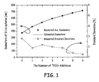
- FIG. 1 is a graph of diameter of silica spheres in nanometers in standard deviation and percentage versus a number of TEOS additions showing measured average diameters, calculated diameters and measured standard deviations.
- FIG. 2 is a top plan view showing an SEM (Scanning Electron Microscope) image of silica spheres in a colloidal suspension before a slow agitation reaction and a centrifugation collection.
- SEM Sccanning Electron Microscope
- FIG. 3 is a top plan view showing an SEM (Scanning Electron Microscope) image of silica spheres in a colloidal suspension after a slow agitation reaction and a centrifugation collection.
- SEM Sccanning Electron Microscope
- FIG. 4 is an SEM image of a top view of a crystalline opal structure with a hexagonal close-packed lattice.
- FIG. 5 is a cross-sectional SEM image of a sample having six layers of spheres.
- FIG. 6 is a cross-sectional SEM image of a sample having thirteen layers of spheres.
- FIG. 7 is a graph of wavelength of maximum reflectance versus incident angle.
- FIG. 8 is a graph of reflectance versus wavelength.
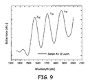
- FIG. 9 is a graph of reflectance versus wavelength.
- FIG. 10A is a cross-sectional diagram of a buried waveguide in an opal structure.
- FIG. 10B is a cross-sectional diagram of a buried waveguide in an inverse opal structure.
- FIG. 11 is a side plan view of a substrate carrying an optical guide supported on either a rib or pillar structure.
- FIG. 12 is a cross-sectional SEM image of a silicon nitride waveguide supported on a silica rib buried in a colloidal opal. A portion of the waveguide is unsupported and is not shown in FIG. 12 .
- FIG. 13A is a side plan view of a substrate carrying an opal structure.
- FIG. 13B is a side plan view of the structure of FIG. 13A following filling of the opal structure.
- FIG. 13C is a side plan view of the structure of FIG. 13B following deposition of a waveguide.
- FIG. 13D is a side plan view of the structure of FIG. 13C following deposition of a second opal structure and filling of the opal structure.
- FIG. 13E is a side plan view of the structure of FIG. 13D following removal of silica spheres leaving an inverse opal structure with buried waveguide.
- PBG Photonic Band Gap
- Periodic structures have taken the form of air holes in a semiconductor material as originally conceived (see, E. Yablonovich, Inhibited spontaneous emission in solid state physics and electronics, Phys. Rev. Lett., Vol. 58, pp. 2059–2062, 1987). More recently, periodic structures have taken the form of air holes in semiconductors films (see, O. Painter, J. Vuckovic, A. Yariv, A. Scherer, J. D. O'Brien, P. D. Dapkus, Two dimensional photonic band gap defect mode laser, Science, Vol. 284, pp.
- the invention further includes opal and inverse opal structures with a waveguide defect carried therein.
- opal and inverse opal structures with a waveguide defect carried therein.
- fcc face centered cubic
- opal opal
- a pseudo-stop-band is one in which the frequency is not completely blocked, but attenuated to some value which is typically by about an order of magnitude.
- the inverse opal is a structure in which the opal acts as a template and the space between the spheres is filled with a suitable dielectric, and the spheres extracted. See, for example Special Section on Electromagnetic Crystal Structures, Design, Synthesis, and Applications, Journal of Lightwave Technology, Vol. 17, pp. 1931–2207, 1999 and Special issue of Advance Materials, Vol. 13, no 6, 2001), and more recently, E. Palacios-Lidon, A.
- a “defect” in any type of well defined PBG structure becomes a cavity at the appropriate stop-band, and should have an extremely high quality factor (Q).
- Q quality factor
- any radiation in this cavity at the appropriate stop-band frequency remains trapped and unable to escape, unless additional defects provide a path for this to occur.
- the creation of the defects in two dimensional structures is much simpler than in self assembled three dimensional structures. While a large number of these self assembled PBGs have been fabricated, the deliberate placing of defects to create cavities with high Qs, and the placement of additional defects to allow trapped radiation to escape has been extremely difficult to achieve.
- the present invention provides a novel technique of creating a defect in the form of a waveguide within a self organized PBG.
- a silica-sphere self assembled PBG is created from a colloidal suspension of spheres which settle to form an opal, in the face centered cubic (fcc) form.
- the structure becomes a photonic band gap structure.
- the colloidal crystals with spheres, “opals” only provides pseudo-stop and pseudo-pass band structures, and the inverted opals, with air/void spheres interconnected with material of a suitably high index show definite pass and stop-bands, and hence the great interest in these inverse opal structures.
- colloidal crystals are formed by packing uniform spheres into 3D arrays, typically face centered cubic (fcc) or hexagonal close packed structures.
- the interstitial space between spheres can be filled by a fluid, such as a liquid metal alkoxide (see, B. T. Holland, C. F. Blanford, A. Stein, Synthesis of Highly Ordered Three-Dimensional Mineral Honeycombs with Macropores, Science, Vol. 281, pp. 538–540, 1998), or a salt solution (see, H. Yan, C. F. Blandford, B. T. Holland, W. H. Smyrl, A.
- the spheres are removed by extraction or dissolution, for example by applying an acid, and the result is a matrix of air holes in a chosen material, a structure useful for PBGs. If the refractive index of the skeleton is high, one obtains a stop-band.
- a fcc 3D structure requires refractive. index of greater than 2.8 for the walls with air voids to obtain a complete stop-band, and also needs to have a low defect crystal structure (see, F. J. P. Schuurmans, D.
- a new technique is provided for obtaining single spherical particles for use in making opal structures.
- a seeding technique is used to synthesize silica spheres of about 710 nm diameters with a pseudo-stop-band at 1550 nm wavelength (see, G. H. Bogush, M. A. Tracy, C. F. Zukoski IV, “Preparation of monodisperse silica particles: Control of size and mass fraction”, J. Non-Crystalline Solids, vol. 104, pp. 95–106, 1988 and S. L. Chen, P. Dong, G.-H. Yang, J.-J.
- TEOS tetraethylorthosilicate
- water 6.0 M
- ammonia 1.8M
- TEOS additions with initial amount (0.2 M) are repeated under the same reaction conditions and constant intervals (4 hrs).
- FIG. 1 is a graph of the diameter of silica spheres in nanometers and standard deviation in percentage versus the number of TEOS additions.
- the spheres were formed using a slow agitation reaction and collection using a centrifuge.
- D s is 375 nm plus/minus 2.8%
- D f is 711 nm plus/minus 1.3% measured across 100 spheres using SEM images.
- FIG. 1 the average diameter of silica spheres measured by the scanning electron microscope in good agreement with the calculated diameters as a function of TEOS additions using Equation 1.
- FIG. 2 is an SEM image of silica spheres in colloidal suspension before a slow agitation reaction and a centrifugation collection and FIG.
- FIG. 3 is an SEM image after slow agitation reaction and centrifugation collection. As illustrated in FIG. 2A , a number of spheres are aggregated or adhered (8.8%). However, after slow agitation and centrifugation collection ( FIG. 3 ), only 0.3% of the spheres are aggregated or adhered.
- the present invention provides a technique for harvesting single spheres.
- Two effective methods are used to prepare high quality silica spheres with reduced aggregation and adhesion. These methods are slow agitation and collection of single spheres with a centrifuge. The slow agitation technique results in a lower probability of collisions between silica spheres. This yields a colloidal suspension having adhered spheres of 3%.
- the centrifugation technique single spheres are collected using the relative difference of sedimentation velocity between singles and doublets with centrifugal force. A separated region with only single spheres can be obtained, using partial sedimentation with the centrifuge. This is a much more effective and faster method than the one using gravitational field (see, P.
- silica spheres can be obtained such as those shown in FIG. 3 having a greatly reduced number of adhered or aggregate spheres of only 0.3%.
- silica spheres can be used to prepare opal structures. These silica spheres are put in a colloidal suspension with a controlled volume fraction in ethanol and used to coat a Silicon substrate. A coating method using a capillary force at the meniscus of the liquid is used in which the convection of the colloidal suspension by heating is employed to avoid the sedimentation of silica spheres.
- a coating method using a capillary force at the meniscus of the liquid is used in which the convection of the colloidal suspension by heating is employed to avoid the sedimentation of silica spheres.
- the Silicon substrate is placed at an angle as it is removed from the colloidal suspension through the meniscus.
- the angle is a declination at 60° measured relative to the plane of the substrate.
- an optimal angle can be selected as desired and may range between about 55° and about 65°.
- an evaporation temperature of 60° C. is used and a declined substrate angle in the colloidal suspension of 60° is provided. This configuration provides a very uniform crystal opal on a 1 cm by 3 cm Silicon substrate. This is illustrated in FIGS.
- opals 4 , 5 and 6 which are, respectively, a top view of an opal with hexagonal closely packed lattice structure, a cross-sectional view of one sample substrate with six layers and a cross-sectional view of another sample substrate with thirteen layers of spheres.
- the thickness of the opals can be controlled by varying the concentration of silica spheres in the colloidal suspensions.
- FIG. 7 is a graph of wavelength ⁇ 0 versus incident angle and shows the measured and calculated positions of the maximum peak ( ⁇ 0 ) of the reflectance spectra, which represent the photonic stop-band behavior, depending upon incident angle.
- the calculated wavelengths of maximum reflectance peak can be estimated by following equations, which combines Bragg's and Snell's laws (see, D. W. McComb, B. M. Treble, C. J. Smith, R. M. De La Rue and N. P. Johnson, “Synthesis and characterization of photonic crystals”, J. Mater.
- the present invention includes the self assembly of colloidal opals and inverse opal photonic bandgap structures and their use in the creation of a waveguide defect within the structures.
- a colloidal opal having a pseudo stop-band in a waveguide buried within is also provided by the present invention.
- the waveguides can be formed in a variety of different materials and are preferably designed to provide a single mode of operation with normal waveguiding and some additional loss due to the presence of the surrounding opal.
- the structures become highly confined and may become multimode. These high confinement waveguides at the pseudo stop-band can be used as narrow band filters.
- the structure perform as an amplifier with improved performance at the stop-band.
- Er doped waveguides with etched gratings at both ends can be optically pumped and will operate as lasers. These structures are more efficient at the pseudo stop-band.
- a defect in the form of a rare earth doped waveguide in this PBG acts as a low threshold photonic bandgap waveguide laser when optically pumped since at the stop-band the spontaneous emission from the inverted rare-earth carries does not escape from the waveguide. Since the PBG prevents the spontaneous emission from escaping, this structure also becomes a highly efficient wide band Amplified Spontaneous Emission (ASE) source. While low transparency amplifiers are also possible, however, the high level of amplified spontaneous emission may degrade performance.
- ASE Amplified Spontaneous Emission
- FIG. 10A is a cross-sectional diagrammatical view of an opal structure 10 carried on a Silicon substrate 12 including a buried waveguide 14 .
- FIG. 10B shows an inverse opal structure 20 on a Silicon substrate 22 carrying a buried waveguide 24 therein.
- the silica opal and the Silicon inverse opal structures can be designed using simulations, for example based upon published codes (see, S. G. Johson, J. D. Joanopoulos, Block iterative frequency domain method for Maxwell's equations in a plane wave basis, Opt. Express, Vol. 8, 173–190, 2001 and P. M. Bell, J. M. Pendry, I. Martin-Moreno, A. J.
- TEOS tetraethyl orthosilicate
- the technique involves the mixing of two mother liquors of TEOS-ethanol and ammonia-water-ethanol and generally leads to spheres in the range of 300 nm to 450 nm diameter, depending on various factors. In one trial, a sphere size of about 350 nm was obtained.
- a modified seeding technique can also be used as discussed in Chen's paper (S. L. Chen, P. Pong, G. H. Yang, J. J. Yang, Characteristic aspects of formation of new particles during growth of monosize silica seeds, J. Colloid. Interface Sci., vol. 180, pp. 237–241, 1996). In this technique, the seeds are first synthesized by the modified Stöber method (see, J. G. Fleming, S-Y.
- the silica opal should be fabricated with very few crystal defects, especially stacking faults, as discussed in (D. J. Norris, Y. A. Vlasov, Chemical Approaches to Three-Dimensional Semiconductor Photonic Crystals, Advanced Materials, Vol. 13, Issue 6, pp. 371–376, 2001). Opals with other spheres may also be fabricated using this technique. Although a Silicon substrate is discussed herein, any appropriate material can be used.
- a silica colloidal opal structure can be obtained when a suspension of the mono-dispersed silica spheres are allowed to settle on the Silicon substrate.
- a meniscus method can be used as discussed above to reduce crystalline defects.
- the declination configuration discussed above can be used to increase the uniformity of the crystal.
- the present invention includes an optical waveguide carried within an opal structure, either opal or inverse opal. Any appropriate technique can be used to obtain such a buried waveguide.
- an optical waveguide 50 is supported on a silica rib 52 carried on the Silicon substrate 54 .
- the waveguide can be any desired structure such as Erbium doped silicon.
- the supporting structure 52 can be an elongated rib or can comprise one or more spaced apart pillars. These can be formed using any appropriate technique such as using deposition and masking techniques to form the desired supporting structure. Similarly, any desired appropriate technique can be used to deposit the waveguide 50 .
- FIG. 12 is an SEM image showing a cleaved opal structure having a waveguide buried therein.
- the guide provides a pseudo stop-band and can be designed to remain single or multimode as desired.
- the top surface of the opal is substantially planar and does not include substantial protrusions despite the introduction of the buried waveguide.
- Erbium or other materials can be doped into the guides during deposition, or alternatively through implantation. The presence of Erbium can be used in the fabrication of high gain lasers because some of the spontaneous emission at the stop-band wavelengths will be coupled back into the guide. It is expected that this increase is more dramatic in an inverse opal structure.
- Reflectors can be placed at either end of the doped guides and pumped at the appropriate wavelength, for example 1480 nm, to provide a very low threshold laser.
- the waveguide can also be used in an inverse opal structure.
- the first step is to fill the interstitial spaces between the sphere of the previously fabricated opal structure.
- LPCVD Low Pressure Chemical Vapor Deposition
- amorphous silicon can be used to fill the voids.
- a colloidal template will emerge from the LPCVD silicon deposition, covered with a thin layer of silicon. This thin layer of silicon must be etched to expose the underlying silica spheres. The spheres can then be removed by dissolution using dilute or buffered HF. It has been suggested that the deposition of silicon is best done at a slightly lower temperature of 550° C. so that complete penetration into the voids will occur. (See, Y.
- Waveguides formed of a material having a dissolution rate in HF which is much lower than silica can be used.
- LPCVD low stress nitride or nitride can be used.
- guides which dissolve such as silica guides, can be used to leave an air guide with protruding sphere surfaces. This is likely to make the guides relative lossy.
- the silica guide is coated with nitride of sufficient thickness on all sides, then the S i O 2 guide will remain after removal of the silica spheres.
- the index of the inverse opal is estimated as 1.63, due to the fact that the air holes comprise of about 0.74 of the structure, and the remainder is Silicon.
- FIGS. 13A–E illustrate another example configuration for forming the buried waveguide.
- a substrate 70 carries a number of layers of opals 72 .
- the opal is filled with an inverse opal filling material.
- material to form a waveguide 74 is deposited and patterned on the structure.
- the waveguide on the filled opal is covered with another layer of opal 76 which is subsequently filled as illustrated in FIG. 13D .
- the opal is etched leaving an inverse opal structure 78 .
- the waveguide can then act as a filter at the stop-bands of the inverse opal.
- the guide can be doped with a rare earth material, such as Erbium or other elements, to provide lasers, optical amplifiers, optical spontaneous emission sources, or other devices.
Abstract
Description
D f=3√{square root over ((1+k)×D s 3)} EQ. 1
where dhkl=√{square root over (2D)}/√{square root over (3)} is the inter-planar spacing for (111) planes, D is the silica sphere diameter, mB is the order of the Bragg reflection, θi is the Bragg angle measured from the normal to the planes, neff is the effective refractive index, Φ=0.74 is the volume fraction of silica spheres in the opals and nsi02=1.447 and nair=1.0 are the refractive index of silica and air, respectively.
where N is the number of layers. In the calculations of wavelengths of qth peak, arbitrary positive integers are used in m and N. The theoretical and experimental wavelengths of qth peak are compared in the Table 1. Using the SEM cross section images of samples, such as shown in
Table 1. Characterization Results of the Wavelengths of qth Peak and the Number of Silica Sphere Layers.
| TABLE 1 | |||||||
| Sample | Dave | |λmeas.pq − | |||||
| #p | [nm] | N | m | q | λcal,pq [nm] | λmeas,pq [nm] | λcal,pq| [nm] |
| 1 | 696 | 6 | 6 | 0 | 1512 | 1525 | 13 |
| 5 | 1 | 1814 | 1870 | 56 | |||
| 4 | 2 | 2268 | 2315 | 47 | |||
| 2 | 696 | 8 | 8 | 0 | 1512 | 1510 | 2 |
| 7 | 1 | 1728 | 1750 | 22 | |||
| 6 | 2 | 2016 | 2038 | 22 | |||
| 5 | 3 | 2419 | 2424 | 5 | |||
| 3 | 718 | 12 | 12 | 0 | 1560 | 1562 | 2 |
| 11 | 1 | 1701 | 1706 | 5 | |||
| 10 | 2 | 1872 | 1865 | 7 | |||
Claims (12)
Priority Applications (6)
| Application Number | Priority Date | Filing Date | Title |
|---|---|---|---|
| US10/801,940 US7106938B2 (en) | 2004-03-16 | 2004-03-16 | Self assembled three-dimensional photonic crystal |
| CNA2005800087644A CN1934475A (en) | 2004-03-16 | 2005-03-08 | Self assembled three-dimensional photonic crystal |
| KR1020067018928A KR20070003941A (en) | 2004-03-16 | 2005-03-08 | Self assembled three-dimensional photonic crystal |
| PCT/US2005/007569 WO2005091028A2 (en) | 2004-03-16 | 2005-03-08 | Self assembled three-dimensional photonic crystal |
| EP05724983A EP1733264A2 (en) | 2004-03-16 | 2005-03-08 | Self assembled three-dimensional photonic crystal |
| JP2007503948A JP2007529783A (en) | 2004-03-16 | 2005-03-08 | Self-assembled three-dimensional photonic crystal |
Applications Claiming Priority (1)
| Application Number | Priority Date | Filing Date | Title |
|---|---|---|---|
| US10/801,940 US7106938B2 (en) | 2004-03-16 | 2004-03-16 | Self assembled three-dimensional photonic crystal |
Publications (2)
| Publication Number | Publication Date |
|---|---|
| US20050206020A1 US20050206020A1 (en) | 2005-09-22 |
| US7106938B2 true US7106938B2 (en) | 2006-09-12 |
Family
ID=34962130
Family Applications (1)
| Application Number | Title | Priority Date | Filing Date |
|---|---|---|---|
| US10/801,940 Active 2024-10-14 US7106938B2 (en) | 2004-03-16 | 2004-03-16 | Self assembled three-dimensional photonic crystal |
Country Status (6)
| Country | Link |
|---|---|
| US (1) | US7106938B2 (en) |
| EP (1) | EP1733264A2 (en) |
| JP (1) | JP2007529783A (en) |
| KR (1) | KR20070003941A (en) |
| CN (1) | CN1934475A (en) |
| WO (1) | WO2005091028A2 (en) |
Cited By (20)
| Publication number | Priority date | Publication date | Assignee | Title |
|---|---|---|---|---|
| US20100294662A1 (en) * | 2009-05-19 | 2010-11-25 | Honeywell International Inc. | Fast response electrochemical organophosphate sensor |
| US20110095389A1 (en) * | 2009-10-23 | 2011-04-28 | The Board Of Trustees Of The Leland Stanford Junior University | Optoelectronic Semiconductor Device and Method of Fabrication |
| US20110121431A1 (en) * | 2009-11-23 | 2011-05-26 | The Board Of Trustees Of The Leland Stanford Junior University | Substrate Comprising a Nanometer-scale Projection Array |
| CN101717989B (en) * | 2009-11-13 | 2012-01-04 | 西安交通大学 | Three-dimensional photonic crystal manufacturing method |
| US20120001284A1 (en) * | 2010-06-30 | 2012-01-05 | President And Fellows Of Harvard College | Silicon nitride light pipes for image sensors |
| US20120155821A1 (en) * | 2010-12-17 | 2012-06-21 | International Business Machines Corporation | Particle filled polymer waveguide |
| US8999857B2 (en) | 2010-04-02 | 2015-04-07 | The Board Of Trustees Of The Leland Stanford Junior University | Method for forming a nano-textured substrate |
| US9000353B2 (en) | 2010-06-22 | 2015-04-07 | President And Fellows Of Harvard College | Light absorption and filtering properties of vertically oriented semiconductor nano wires |
| US9054008B2 (en) | 2010-06-22 | 2015-06-09 | Zena Technologies, Inc. | Solar blind ultra violet (UV) detector and fabrication methods of the same |
| US9082673B2 (en) | 2009-10-05 | 2015-07-14 | Zena Technologies, Inc. | Passivated upstanding nanostructures and methods of making the same |
| US9123841B2 (en) | 2009-12-08 | 2015-09-01 | Zena Technologies, Inc. | Nanowire photo-detector grown on a back-side illuminated image sensor |
| US9177985B2 (en) | 2009-06-04 | 2015-11-03 | Zena Technologies, Inc. | Array of nanowires in a single cavity with anti-reflective coating on substrate |
| US9304035B2 (en) | 2008-09-04 | 2016-04-05 | Zena Technologies, Inc. | Vertical waveguides with various functionality on integrated circuits |
| US9343490B2 (en) | 2013-08-09 | 2016-05-17 | Zena Technologies, Inc. | Nanowire structured color filter arrays and fabrication method of the same |
| US9406709B2 (en) | 2010-06-22 | 2016-08-02 | President And Fellows Of Harvard College | Methods for fabricating and using nanowires |
| US9410843B2 (en) | 2008-09-04 | 2016-08-09 | Zena Technologies, Inc. | Nanowire arrays comprising fluorescent nanowires and substrate |
| US9429723B2 (en) | 2008-09-04 | 2016-08-30 | Zena Technologies, Inc. | Optical waveguides in image sensors |
| US9478685B2 (en) | 2014-06-23 | 2016-10-25 | Zena Technologies, Inc. | Vertical pillar structured infrared detector and fabrication method for the same |
| US9515218B2 (en) | 2008-09-04 | 2016-12-06 | Zena Technologies, Inc. | Vertical pillar structured photovoltaic devices with mirrors and optical claddings |
| US9543458B2 (en) | 2010-12-14 | 2017-01-10 | Zena Technologies, Inc. | Full color single pixel including doublet or quadruplet Si nanowires for image sensors |
Families Citing this family (12)
| Publication number | Priority date | Publication date | Assignee | Title |
|---|---|---|---|---|
| US7078697B2 (en) * | 2004-10-07 | 2006-07-18 | Raytheon Company | Thermally powered terahertz radiation source using photonic crystals |
| CN100532496C (en) * | 2006-05-26 | 2009-08-26 | 中国科学院化学研究所 | Method for reinforcing fluorescence intensity for rare earth three primary colors phosphor powder |
| US8228129B2 (en) * | 2008-11-06 | 2012-07-24 | Raytheon Company | Photonic crystal resonant defect cavities with nano-scale oscillators for generation of terahertz or infrared radiation |
| US8261557B2 (en) * | 2008-12-05 | 2012-09-11 | Raytheon Company | Heat transfer devices based on thermodynamic cycling of a photonic crystal with coupled resonant defect cavities |
| JP5677227B2 (en) * | 2010-07-28 | 2015-02-25 | 京セラ株式会社 | Opal, method for producing the same, paint and printed matter using the same |
| GB2505895B (en) * | 2012-09-13 | 2018-03-21 | De La Rue Int Ltd | Method for forming photonic crystal materials |
| KR101463938B1 (en) * | 2013-01-31 | 2014-11-26 | 서강대학교산학협력단 | Method and device of forming structure of photo crystal |
| US10330832B2 (en) | 2015-06-25 | 2019-06-25 | Apple Inc. | High-luminance surface |
| US10684397B2 (en) | 2015-09-08 | 2020-06-16 | Apple Inc. | Refractive coatings for a colored surface of an electronic device |
| US10527765B2 (en) * | 2015-09-29 | 2020-01-07 | Apple Inc. | Surfaces having structured optical appearances |
| KR101791745B1 (en) * | 2015-10-15 | 2017-11-20 | 서강대학교산학협력단 | Manufacturing method of photonic crystal structure and device used therein |
| US11693153B2 (en) * | 2019-11-26 | 2023-07-04 | Hrl Laboratories, Llc | Omnidirectional and thermally durable infrared reflectors, and methods for making the same |
Citations (39)
| Publication number | Priority date | Publication date | Assignee | Title |
|---|---|---|---|---|
| WO1999001766A1 (en) | 1997-07-04 | 1999-01-14 | Universiteit Utrecht | A metal particle, its preparation and use, and a material or device comprising the metal particle |
| WO1999047570A1 (en) | 1998-03-18 | 1999-09-23 | University Of Rochester | Macromolecular self-assembly of microstructures, nanostructures, objects and mesoporous solids |
| WO2000021905A1 (en) | 1998-10-13 | 2000-04-20 | Alliedsignal Inc. | Three dimensionally periodic structural assemblies on nanometer and longer scales |
| WO2000050771A1 (en) | 1999-02-25 | 2000-08-31 | Alliedsignal Inc. | Actuators using double-layer charging of high surface area materials |
| US6139626A (en) | 1998-09-04 | 2000-10-31 | Nec Research Institute, Inc. | Three-dimensionally patterned materials and methods for manufacturing same using nanocrystals |
| EP1081513A1 (en) | 1999-09-01 | 2001-03-07 | Lucent Technologies Inc. | Process for fabricating a colloidal crystal having substantial three-dimensional order |
| WO2001018283A1 (en) | 1999-09-07 | 2001-03-15 | Qinetiq Limited | Colloidal photonic crystals |
| US6228340B1 (en) | 1997-08-25 | 2001-05-08 | The Regents Of The University Of California | Method for the production of macroporous ceramics |
| WO2001055484A2 (en) | 2000-01-28 | 2001-08-02 | The Governing Council Of The University Of Toronto | Photonic bandgap materials based on silicon |
| WO2001062830A2 (en) | 2000-02-22 | 2001-08-30 | Eugenia Kumacheva | Polymer-based nanocomposite materials and methods of production thereof |
| WO2001066833A1 (en) | 2000-03-06 | 2001-09-13 | University Of Connecticut | Apparatus and method for fabrication of photonic crystals |
| WO2001086038A2 (en) | 2000-05-05 | 2001-11-15 | Universidad Politecnica De Valencia | Photonic bandgap materials based on germanium |
| WO2001096635A2 (en) | 2000-06-15 | 2001-12-20 | Merck Patent Gmbh | A method for producing sphere-based crystals |
| US20020045030A1 (en) | 2000-10-16 | 2002-04-18 | Ozin Geoffrey Alan | Method of self-assembly and optical applications of crystalline colloidal patterns on substrates |
| US20020062782A1 (en) | 2000-11-28 | 2002-05-30 | Norris David J. | Self-assembled photonic crystals and methods for manufacturing same |
| WO2002044301A2 (en) | 2000-11-30 | 2002-06-06 | Merck Patent Gmbh | Particles with opalescent effect |
| US6414043B1 (en) | 1998-06-26 | 2002-07-02 | University Of Pittsburgh | Hydrogel materials with crystalline colloidal array of watervoids for detection and macromolecule separations |
| WO2002059656A2 (en) | 2001-01-25 | 2002-08-01 | Omniguide Communications | Low-loss photonic crystal waveguide having large core radius |
| WO2002059663A1 (en) | 2001-01-25 | 2002-08-01 | Omniguide Communications | Photonic crystal optical waveguides having tailored dispersion profiles |
| WO2002061467A2 (en) | 2001-01-31 | 2002-08-08 | Omniguide Communications | Electromagnetic mode conversion in photonic crystal multimode waveguides |
| US20020126713A1 (en) | 2000-10-26 | 2002-09-12 | Mihai Ibanescu | Dielectric waveguide with transverse index variation that support a zero group velocity mode at a non-zero longitudinal wavevector |
| EP1247820A1 (en) | 2001-03-29 | 2002-10-09 | Agfa-Gevaert | Method of preparing polymer particles having narrow particle size distribution |
| WO2002091028A2 (en) | 2001-05-03 | 2002-11-14 | Colorado School Of Mines | Devices employing colloidal-sized particles |
| US20020173610A1 (en) | 2001-03-29 | 2002-11-21 | Huub Van Aert | Method of preparing polymer particles having narrow particle size distribution |
| US20020189947A1 (en) | 2001-06-13 | 2002-12-19 | Eksigent Technologies Llp | Electroosmotic flow controller |
| WO2003007663A1 (en) | 2001-07-10 | 2003-01-23 | Trustees Of Princeton University | Micro-lens arrays for display intensity enhancement |
| US20030021518A1 (en) | 2001-06-01 | 2003-01-30 | D-Wave Systems, Inc. | Optical transformer device |
| US20030063426A1 (en) | 2001-08-29 | 2003-04-03 | D-Wave Systems, Inc. | Microsphere optical device |
| US20030103721A1 (en) | 2001-12-03 | 2003-06-05 | Aravind Padmanabhan | Optical demultiplexer based on three-dimensionally periodic photonic crystals |
| US6589629B1 (en) | 2000-09-11 | 2003-07-08 | Lucent Technologies Inc. | Process for fabricating patterned, functionalized particles and article formed from particles |
| US20030136946A1 (en) | 2000-02-22 | 2003-07-24 | Eugenia Kumacheva | Polymer-based nanocomposite materials and methods of production thereof |
| US20030143081A1 (en) | 2002-01-31 | 2003-07-31 | Eksigent Technologies Llc, A California Corporation | Variable potential electrokinetic device |
| US20030148088A1 (en) | 2002-02-07 | 2003-08-07 | Aravind Padmanabhan | Light emitting photonic crystals |
| US20030156319A1 (en) | 2000-01-28 | 2003-08-21 | Sajeev John | Photonic bandgap materials based on silicon |
| US20030206806A1 (en) | 2002-05-01 | 2003-11-06 | Paul Phillip H. | Bridges, elements and junctions for electroosmotic flow systems |
| US6680013B1 (en) | 1999-04-15 | 2004-01-20 | Regents Of The University Of Minnesota | Synthesis of macroporous structures |
| US20040017834A1 (en) | 2002-07-23 | 2004-01-29 | Sundar Vikram C. | Creating photon atoms |
| US20040020423A1 (en) | 2002-07-31 | 2004-02-05 | Lewis John South | Layer-by-layer assembly of photonic crystals |
| US6898362B2 (en) * | 2002-01-17 | 2005-05-24 | Micron Technology Inc. | Three-dimensional photonic crystal waveguide structure and method |
-
2004
- 2004-03-16 US US10/801,940 patent/US7106938B2/en active Active
-
2005
- 2005-03-08 EP EP05724983A patent/EP1733264A2/en not_active Withdrawn
- 2005-03-08 CN CNA2005800087644A patent/CN1934475A/en active Pending
- 2005-03-08 JP JP2007503948A patent/JP2007529783A/en not_active Withdrawn
- 2005-03-08 KR KR1020067018928A patent/KR20070003941A/en not_active Application Discontinuation
- 2005-03-08 WO PCT/US2005/007569 patent/WO2005091028A2/en active Application Filing
Patent Citations (64)
| Publication number | Priority date | Publication date | Assignee | Title |
|---|---|---|---|---|
| WO1999001766A1 (en) | 1997-07-04 | 1999-01-14 | Universiteit Utrecht | A metal particle, its preparation and use, and a material or device comprising the metal particle |
| US6228340B1 (en) | 1997-08-25 | 2001-05-08 | The Regents Of The University Of California | Method for the production of macroporous ceramics |
| WO1999047570A1 (en) | 1998-03-18 | 1999-09-23 | University Of Rochester | Macromolecular self-assembly of microstructures, nanostructures, objects and mesoporous solids |
| US6414043B1 (en) | 1998-06-26 | 2002-07-02 | University Of Pittsburgh | Hydrogel materials with crystalline colloidal array of watervoids for detection and macromolecule separations |
| US6139626A (en) | 1998-09-04 | 2000-10-31 | Nec Research Institute, Inc. | Three-dimensionally patterned materials and methods for manufacturing same using nanocrystals |
| WO2000021905A1 (en) | 1998-10-13 | 2000-04-20 | Alliedsignal Inc. | Three dimensionally periodic structural assemblies on nanometer and longer scales |
| US6261469B1 (en) | 1998-10-13 | 2001-07-17 | Honeywell International Inc. | Three dimensionally periodic structural assemblies on nanometer and longer scales |
| US6517763B1 (en) | 1998-10-13 | 2003-02-11 | Alliedsignal, Inc. | Three dimensionally periodic structural assemblies in nanometer and longer scales |
| US20010019037A1 (en) | 1998-10-13 | 2001-09-06 | Anvar Zakhidov | Three dimensionally periodic structural assemblies on nanometer and longer scales |
| WO2000050771A1 (en) | 1999-02-25 | 2000-08-31 | Alliedsignal Inc. | Actuators using double-layer charging of high surface area materials |
| US6555945B1 (en) | 1999-02-25 | 2003-04-29 | Alliedsignal Inc. | Actuators using double-layer charging of high surface area materials |
| US6680013B1 (en) | 1999-04-15 | 2004-01-20 | Regents Of The University Of Minnesota | Synthesis of macroporous structures |
| EP1081513A1 (en) | 1999-09-01 | 2001-03-07 | Lucent Technologies Inc. | Process for fabricating a colloidal crystal having substantial three-dimensional order |
| US6436187B1 (en) | 1999-09-01 | 2002-08-20 | Agere Systems Guardian Corp. | Process for fabricating article having substantial three-dimensional order |
| US6797057B1 (en) * | 1999-09-07 | 2004-09-28 | Qinetiq Limited | Colloidal photonic crystals |
| WO2001018283A1 (en) | 1999-09-07 | 2001-03-15 | Qinetiq Limited | Colloidal photonic crystals |
| US20030156319A1 (en) | 2000-01-28 | 2003-08-21 | Sajeev John | Photonic bandgap materials based on silicon |
| WO2001055484A2 (en) | 2000-01-28 | 2001-08-02 | The Governing Council Of The University Of Toronto | Photonic bandgap materials based on silicon |
| US20030136946A1 (en) | 2000-02-22 | 2003-07-24 | Eugenia Kumacheva | Polymer-based nanocomposite materials and methods of production thereof |
| WO2001062830A2 (en) | 2000-02-22 | 2001-08-30 | Eugenia Kumacheva | Polymer-based nanocomposite materials and methods of production thereof |
| WO2001066833A1 (en) | 2000-03-06 | 2001-09-13 | University Of Connecticut | Apparatus and method for fabrication of photonic crystals |
| WO2001086038A2 (en) | 2000-05-05 | 2001-11-15 | Universidad Politecnica De Valencia | Photonic bandgap materials based on germanium |
| US6863847B2 (en) * | 2000-06-15 | 2005-03-08 | Em Industries, Inc. | Method for producing sphere-based crystals |
| WO2001096635A2 (en) | 2000-06-15 | 2001-12-20 | Merck Patent Gmbh | A method for producing sphere-based crystals |
| US20020024163A1 (en) | 2000-06-15 | 2002-02-28 | Em Industries, Inc. | Method for producing sphere-based crystals |
| US6589629B1 (en) | 2000-09-11 | 2003-07-08 | Lucent Technologies Inc. | Process for fabricating patterned, functionalized particles and article formed from particles |
| US20020045030A1 (en) | 2000-10-16 | 2002-04-18 | Ozin Geoffrey Alan | Method of self-assembly and optical applications of crystalline colloidal patterns on substrates |
| WO2002033461A2 (en) | 2000-10-16 | 2002-04-25 | Ozin Geoffrey A | Method of self-assembly and optical applications of crystalline colloidal patterns on substrates |
| US20020126713A1 (en) | 2000-10-26 | 2002-09-12 | Mihai Ibanescu | Dielectric waveguide with transverse index variation that support a zero group velocity mode at a non-zero longitudinal wavevector |
| US6858079B2 (en) * | 2000-11-28 | 2005-02-22 | Nec Laboratories America, Inc. | Self-assembled photonic crystals and methods for manufacturing same |
| US20020062782A1 (en) | 2000-11-28 | 2002-05-30 | Norris David J. | Self-assembled photonic crystals and methods for manufacturing same |
| WO2002044301A2 (en) | 2000-11-30 | 2002-06-06 | Merck Patent Gmbh | Particles with opalescent effect |
| US20030008771A1 (en) | 2000-11-30 | 2003-01-09 | Em Industries, Inc. | 3D structural siliceous color pigments |
| US20040013379A1 (en) | 2001-01-25 | 2004-01-22 | Omniguide Communications, A Delaware Corporation | Low-loss photonic crystal waveguide having large core radius |
| WO2002059656A2 (en) | 2001-01-25 | 2002-08-01 | Omniguide Communications | Low-loss photonic crystal waveguide having large core radius |
| US6625364B2 (en) | 2001-01-25 | 2003-09-23 | Omniguide Communications | Low-loss photonic crystal waveguide having large core radius |
| US20020164137A1 (en) | 2001-01-25 | 2002-11-07 | Johnson Steven G. | Low-loss photonic crystal waveguide having large core radius |
| US20020176676A1 (en) | 2001-01-25 | 2002-11-28 | Johnson Steven G. | Photonic crystal optical waveguides having tailored dispersion profiles |
| WO2002059663A1 (en) | 2001-01-25 | 2002-08-01 | Omniguide Communications | Photonic crystal optical waveguides having tailored dispersion profiles |
| US20030185505A1 (en) | 2001-01-31 | 2003-10-02 | Omniguide Communications, A Delaware Corporation | Electromagnetic mode conversion in photonic crystal multimode waveguides |
| US20030031407A1 (en) | 2001-01-31 | 2003-02-13 | Ori Weisberg | Electromagnetic mode conversion in photonic crystal multimode waveguides |
| US6563981B2 (en) | 2001-01-31 | 2003-05-13 | Omniguide Communications | Electromagnetic mode conversion in photonic crystal multimode waveguides |
| WO2002061467A2 (en) | 2001-01-31 | 2002-08-08 | Omniguide Communications | Electromagnetic mode conversion in photonic crystal multimode waveguides |
| US6800709B2 (en) * | 2001-03-29 | 2004-10-05 | Agfa-Gevaert N.V. | Method of preparing polymer particles having narrow particle size distribution |
| US20020173610A1 (en) | 2001-03-29 | 2002-11-21 | Huub Van Aert | Method of preparing polymer particles having narrow particle size distribution |
| EP1247820A1 (en) | 2001-03-29 | 2002-10-09 | Agfa-Gevaert | Method of preparing polymer particles having narrow particle size distribution |
| WO2002091028A2 (en) | 2001-05-03 | 2002-11-14 | Colorado School Of Mines | Devices employing colloidal-sized particles |
| US20030012657A1 (en) | 2001-05-03 | 2003-01-16 | Marr David W.M. | Devices employing colloidal-sized particles |
| US20030021518A1 (en) | 2001-06-01 | 2003-01-30 | D-Wave Systems, Inc. | Optical transformer device |
| WO2002101474A2 (en) | 2001-06-13 | 2002-12-19 | Eksigent Technologies, Llc | Flow control systems |
| US20020189947A1 (en) | 2001-06-13 | 2002-12-19 | Eksigent Technologies Llp | Electroosmotic flow controller |
| US20020195344A1 (en) | 2001-06-13 | 2002-12-26 | Neyer David W. | Combined electroosmotic and pressure driven flow system |
| US20030020399A1 (en) | 2001-07-10 | 2003-01-30 | Sven Moller | Micro-lens arrays for display intensity enhancement |
| WO2003007663A1 (en) | 2001-07-10 | 2003-01-23 | Trustees Of Princeton University | Micro-lens arrays for display intensity enhancement |
| US20030063426A1 (en) | 2001-08-29 | 2003-04-03 | D-Wave Systems, Inc. | Microsphere optical device |
| US20030103721A1 (en) | 2001-12-03 | 2003-06-05 | Aravind Padmanabhan | Optical demultiplexer based on three-dimensionally periodic photonic crystals |
| US6898362B2 (en) * | 2002-01-17 | 2005-05-24 | Micron Technology Inc. | Three-dimensional photonic crystal waveguide structure and method |
| US20030143081A1 (en) | 2002-01-31 | 2003-07-31 | Eksigent Technologies Llc, A California Corporation | Variable potential electrokinetic device |
| US20030148088A1 (en) | 2002-02-07 | 2003-08-07 | Aravind Padmanabhan | Light emitting photonic crystals |
| US20030206806A1 (en) | 2002-05-01 | 2003-11-06 | Paul Phillip H. | Bridges, elements and junctions for electroosmotic flow systems |
| WO2004009724A2 (en) | 2002-07-23 | 2004-01-29 | Massachusetts Institute Of Technology | Creating photon atoms |
| US20040017834A1 (en) | 2002-07-23 | 2004-01-29 | Sundar Vikram C. | Creating photon atoms |
| US20040020423A1 (en) | 2002-07-31 | 2004-02-05 | Lewis John South | Layer-by-layer assembly of photonic crystals |
| WO2004013383A1 (en) | 2002-07-31 | 2004-02-12 | Mcnc Research And Development Institute | Layer-by-layer assembly of photonic crystals |
Non-Patent Citations (39)
| Title |
|---|
| "A Three-Dimensional Optical Photonic Crystal", by S. Lin et al., Journal of Lightwave Technology, vol. 17, No. 11, Nov. 1999, pp. 1944-1947. |
| "High-Resolution Particle Separation by Sedimentation Field-Flow Fractionation", by F. Yang et al., Journal of Colloid and Interface Science, vol. 60, No. 3, Jul. 1, 1977, pp. 574-577. |
| "Optical coupling between monocrystalline colloidal crystals and a planar waveguide", by Y. Zhao et al., Applied Physics Letters, vol. 75, No. 23, pp. 3596-3598, (Dec. 6, 1999). |
| "Optical Demultiplexing in a Planar Waveguide with Colloidal Crystal", by I. Avrutsky et al., IEEE Photonics Technology Letters, vol. 12, No. 12, pp. 1647-1649, (Dec. 12, 2000). |
| "Photonic Band Engineering in Opals by Growth of Si/Ge Multilayer Shells", by F. Garcia-Santamaria et al., Adv. Mater. 2003, 15, No. 10, pp. 788-792. |
| "Synthesis and Characterization of Monodisperse Core-Shell Colloidal Spheres of Zinc Sulfide and Silica", by K. Velikov et al., Langmuir 2001, 17, pp. 4779-4786. |
| "Synthetic Opals Made by the Langmuir-Blodgett Method", by M. Bardosova et al., Preparation and Characterization, Elsevier Sequoia, NL, vol. 437, No. 1-2, Aug. 1, 2003, pp. 276-279. |
| "Tuning the Properties of Photonic Films from Polymer Beads by Chemistry", by M. Egen et al., Chem. Mater: 2002, 14, pp. 2176-2183. |
| "Two-dimensional colloidal crystal corrugated waveguides", by Y. Zhao et al., Optics Letters, vol. 24, No. 12, pp. 817-819, (Jun. 15, 1999). |
| B. T. Holland, C. F. Blanford, A. Stein, Synthesis of Highly Ordered Three-Dimensional Mineral Honeycombs with Macropores, Science, vol. 281, pp. 538-540, 1998. |
| B. Temelkuran, M. Bayindir, E. Ozbay, R. Biswas, M. M. Sigalas, G. Tuttle, K. M. Ho, Photonic crystal-based resonant antenna with a very high directivity, J. Appl. Phys., vol. 87, pp. 603-605, 2000. |
| C.F. Blanford, R.C. Schroden, M. Al-Daous, A. Stein, "Tuning solvent-dependent color changes of three-dimensionally ordered macroporous (3DOM) materials through compositional and geometric modifications", Adv. Mater., vol. 13, pp. 26-29, Jan. 2001. |
| D. J. Norris, Y. A. Vlasov, Chemical Approaches to Three-Dimensional Semiconductor Photonic Crystals, Advanced Materials, vol. 13, Issue 6, pp. 371-376, 2001. |
| D.W. McComb, B.M. Treble, C.J. Smith, R.M. De La Rue and N. P. Johnson, "Synthesis and characterization of photonic crystals", J. Mater. Chem., vol. 11, pp. 142-148, 2001. |
| E. Palacios-Lidon, A. Blanco, M. Ibisate, F. Meseguer, C. Lopez, J. Sanchez-Dehesa, Optical study of the full photonic band gap in silicon inverse opals, Appl. Phys. Lett., vol. 81, No. 21, pp. 4925-4927, 2002. |
| E. R. Brown, O. B. McMahon, High zenithal directivity from a dipole antenna on a photonic crystal, Appl. Phys. Lett., vol. 68, pp. 1300-1302, 1996. |
| E. Yablonovich, Inhibited spontaneous emission in solid state physics and electronics, Phys. Rev. Lett., vol. 58, pp. 2059-2062, 1987. |
| F. J. P. Schuurmans, D. Vanmaekelbergh, J. van de Lagemaat, A. Lagendijk, Strongly Photonic Macroporous Gallium Phosphide Networks. Science vol. 284, pp. 141-143, 1999. |
| G.H. Bogush, M.A. Tracy, C.F. Zukoski IV, "Preparation of monodisperse silica particles: Control of size and mass fraction", J. Non-Crystalline Solids, vol. 104, pp. 95-106, 1988. |
| H. Yan, C. F. Blandford, B. T. Holland, W. H. Smyrl, A. Stein, General Synthesis of Periodic Macro-porous Solids by Templated Salt Precipitation and Chemical Conversion, Chem. Mater., vol. 12, pp. 1134-1141, 2000. |
| Invitation to Pay Additional Fees/Communication Relating to the Results of the Partial International Search for PCT/US2005/007569. |
| J. E. G. J. Wijnhoven, W. L. Vos, Preparation of photonic crystals made of air spheres in Titania, Science, vol. 281, pp. 802-804, 1998. |
| J. G. Fleming, S-Y, Lin, Three dimensional photonic crystal with a stop band from 1.35 to 1.95mum, Optics Lett., vol. 24, pp. 49-51, 1999. |
| K. R. Williams, R. S. Muller, Etch rates for micromachining processing, J. Microelectromechanical Systems, vol. 5, pp. 256-269, 1996. |
| Notification of Transmittal of the International Search Report and the Written Opinion of the International Search Authority for PCT/US2005/007569. |
| O. Painter, J. Vuckovic, A. Yariv, A. Scherer, J. D. O'Brien, P. D. Dapkus, Two dimensional photonic band gap defect mode laser, Science, vol. 284, pp. 1819-1821, 1999. |
| P. Jiang, J.F. Bertone, K.S. Hwang, V.L. Colvin, "Single-Crystal colloidal multilayers of controlled thickness", Chem. Mater., vol. 11, pp. 2132-2140, 1999. |
| P. M. Bell, J. M. Pendry, I. Martin-Moreno, A. J. Ward, A program for calculating photonic band structures and transmission coefficients of complex structures, comput. Phys. commun., vol. 85, pp. 306-322, 1995. |
| P. Ni, P. Dong, B. Cheng, X. Li, D. Zhang, "Synthetic SiO2 opals", Adv. Mater. vol. 13, pp. 437-441, Mar. 2001. |
| S. G. Johnson, J. D. Joanopoulos, Block iterative frequency domain method for Maxwell's equations in a plane wave basis, Opt. Express, vol. 8, 173-190, 2001. |
| S. John, K. Busch, Photonic bandgap formation and tunability in certain self organizing systems, Journal of Lightwave Technology, vol. 17, pp. 1931-1943, 1999. |
| S. Noda, K. Tomoda, N. Yamanoto, A. Chutinan, "Full three-dimensional photonic bandgap crystals at near-infrared wavelengths", Science, vol. 289, pp. 604-606, Jul., 2000. |
| S.L. Chen, P. Dong, G.-H. Yang, J.-J. Yang, "Characteristic aspects of formation of new particles during the growth of monosize silica seeds", Journal of Colloid and Interface Science, vol. 180, pp. 237-241, 1996. |
| Special Feature Section on Photonic Crystal Structures and applications, IEEE J. Quantum Electronics, vol. 38, Jul. 2002. Dimensional photonic. |
| Special issue of Advance Materials, vol. 13, No. 6, p. 369, 2001. |
| Special Section on Electromagnetic Crystal Structures, Design, Synthesis, and Applications, Journal of Lightwave Technology, vol. 17, pp. 1944-1947, 1999. |
| W. Stober, A. Fink, E. Bohn, "Controlled growth of monodisperse silica spheres in the micron size range", J. Colloid and Interf. Sci., vol. 26, pp. 62-69, 1968. |
| Y. Matsui, M. Ishino, T. Fujita, H. Serizawa, T. Kajiwra, A novel measurement technique of loss and facet reflectivity for semiconductor optical waveguides, SPIEvol. 651, Integrated Optical Circuit Engineering III, 1986. |
| Y.A. Vlasov, X.-Z. Bo, J.C. Sturm, D.J. Norris, "On-chip natural assembly of silicon photonic bandgap crystals", Nature, vol. 414, pp. 289-293, Nov. 2001. |
Cited By (27)
| Publication number | Priority date | Publication date | Assignee | Title |
|---|---|---|---|---|
| US9601529B2 (en) | 2008-09-04 | 2017-03-21 | Zena Technologies, Inc. | Light absorption and filtering properties of vertically oriented semiconductor nano wires |
| US9515218B2 (en) | 2008-09-04 | 2016-12-06 | Zena Technologies, Inc. | Vertical pillar structured photovoltaic devices with mirrors and optical claddings |
| US9429723B2 (en) | 2008-09-04 | 2016-08-30 | Zena Technologies, Inc. | Optical waveguides in image sensors |
| US9410843B2 (en) | 2008-09-04 | 2016-08-09 | Zena Technologies, Inc. | Nanowire arrays comprising fluorescent nanowires and substrate |
| US9337220B2 (en) | 2008-09-04 | 2016-05-10 | Zena Technologies, Inc. | Solar blind ultra violet (UV) detector and fabrication methods of the same |
| US9304035B2 (en) | 2008-09-04 | 2016-04-05 | Zena Technologies, Inc. | Vertical waveguides with various functionality on integrated circuits |
| US20100294662A1 (en) * | 2009-05-19 | 2010-11-25 | Honeywell International Inc. | Fast response electrochemical organophosphate sensor |
| US9177985B2 (en) | 2009-06-04 | 2015-11-03 | Zena Technologies, Inc. | Array of nanowires in a single cavity with anti-reflective coating on substrate |
| US9082673B2 (en) | 2009-10-05 | 2015-07-14 | Zena Technologies, Inc. | Passivated upstanding nanostructures and methods of making the same |
| US20110095389A1 (en) * | 2009-10-23 | 2011-04-28 | The Board Of Trustees Of The Leland Stanford Junior University | Optoelectronic Semiconductor Device and Method of Fabrication |
| US8896077B2 (en) | 2009-10-23 | 2014-11-25 | The Board Of Trustees Of The Leland Stanford Junior University | Optoelectronic semiconductor device and method of fabrication |
| CN101717989B (en) * | 2009-11-13 | 2012-01-04 | 西安交通大学 | Three-dimensional photonic crystal manufacturing method |
| US8318604B2 (en) | 2009-11-23 | 2012-11-27 | The Board Of Trustees Of The Leland Stanford Junior University | Substrate comprising a nanometer-scale projection array |
| US20110121431A1 (en) * | 2009-11-23 | 2011-05-26 | The Board Of Trustees Of The Leland Stanford Junior University | Substrate Comprising a Nanometer-scale Projection Array |
| US9123841B2 (en) | 2009-12-08 | 2015-09-01 | Zena Technologies, Inc. | Nanowire photo-detector grown on a back-side illuminated image sensor |
| US9263613B2 (en) | 2009-12-08 | 2016-02-16 | Zena Technologies, Inc. | Nanowire photo-detector grown on a back-side illuminated image sensor |
| US8999857B2 (en) | 2010-04-02 | 2015-04-07 | The Board Of Trustees Of The Leland Stanford Junior University | Method for forming a nano-textured substrate |
| US9000353B2 (en) | 2010-06-22 | 2015-04-07 | President And Fellows Of Harvard College | Light absorption and filtering properties of vertically oriented semiconductor nano wires |
| US9406709B2 (en) | 2010-06-22 | 2016-08-02 | President And Fellows Of Harvard College | Methods for fabricating and using nanowires |
| US9054008B2 (en) | 2010-06-22 | 2015-06-09 | Zena Technologies, Inc. | Solar blind ultra violet (UV) detector and fabrication methods of the same |
| US20120001284A1 (en) * | 2010-06-30 | 2012-01-05 | President And Fellows Of Harvard College | Silicon nitride light pipes for image sensors |
| US8890271B2 (en) * | 2010-06-30 | 2014-11-18 | Zena Technologies, Inc. | Silicon nitride light pipes for image sensors |
| US9543458B2 (en) | 2010-12-14 | 2017-01-10 | Zena Technologies, Inc. | Full color single pixel including doublet or quadruplet Si nanowires for image sensors |
| US20120155821A1 (en) * | 2010-12-17 | 2012-06-21 | International Business Machines Corporation | Particle filled polymer waveguide |
| US8873919B2 (en) * | 2010-12-17 | 2014-10-28 | International Business Machines Corporation | Particle filled polymer waveguide |
| US9343490B2 (en) | 2013-08-09 | 2016-05-17 | Zena Technologies, Inc. | Nanowire structured color filter arrays and fabrication method of the same |
| US9478685B2 (en) | 2014-06-23 | 2016-10-25 | Zena Technologies, Inc. | Vertical pillar structured infrared detector and fabrication method for the same |
Also Published As
| Publication number | Publication date |
|---|---|
| JP2007529783A (en) | 2007-10-25 |
| KR20070003941A (en) | 2007-01-05 |
| EP1733264A2 (en) | 2006-12-20 |
| WO2005091028A3 (en) | 2005-11-10 |
| US20050206020A1 (en) | 2005-09-22 |
| WO2005091028A2 (en) | 2005-09-29 |
| CN1934475A (en) | 2007-03-21 |
Similar Documents
| Publication | Publication Date | Title |
|---|---|---|
| US7106938B2 (en) | Self assembled three-dimensional photonic crystal | |
| US6888994B2 (en) | Optical device | |
| Meseguer et al. | Synthesis of inverse opals | |
| Birner et al. | Silicon‐based photonic crystals | |
| Xia et al. | Photonic crystals | |
| Galisteo et al. | Self-assembly approach to optical metamaterials | |
| US20060137601A1 (en) | Method of synthesis of 3d silicon colloidal photonic crystals by micromolding in inverse silica opal (miso) | |
| US20030156319A1 (en) | Photonic bandgap materials based on silicon | |
| Mihi et al. | Surface resonant modes in colloidal photonic crystals | |
| Dai et al. | 2D inverse periodic opal structures in single crystal diamond with incorporated silicon-vacancy color centers | |
| Zhong et al. | A facile way to introduce planar defects into colloidal photonic crystals for pronounced passbands | |
| Golubev et al. | Three-dimensional ordered silicon-based nanostructures in opal matrix: preparation and photonic properties | |
| Almeida et al. | Sol–gel photonic bandgap materials and structures | |
| Gorelik et al. | Raman scattering in three-dimensional photonic crystals | |
| Goncalves et al. | Process optimization of sol–gel derived colloidal photonic crystals | |
| Nair et al. | Infiltration of ZnO in polymeric photonic crystal by the sol–gel process | |
| CA2398632C (en) | Photonic bandgap materials based on silicon | |
| Thu et al. | Experimental study of 3d self-assembled photonic crystals and colloidal core-shell semiconductor quantum dots | |
| Baek et al. | Self-assembled photonic crystal waveguides | |
| Romanov et al. | Three-dimensional anisotropic photonic crystals working in the visible | |
| Zheng et al. | Investigation of infrared photonic crystal slab with defect waveguides | |
| Weisbuch et al. | Photonic crystals | |
| Khokhar | Opal Based 3D Photonic Crystals | |
| Almeida et al. | Sol–gel derived photonic bandgap structures | |
| LI et al. | Fabrication of germanium inverse opal photonic crystal with a complete three-dimensional bandgap in mid infrared range |
Legal Events
| Date | Code | Title | Description |
|---|---|---|---|
| AS | Assignment |
Owner name: REGENTS OF THE UNVERISITY OF MINNESOTA, MINNESOTA Free format text: ASSIGNMENT OF ASSIGNORS INTEREST;ASSIGNORS:BAEK, KANG-HYUN;GOPINATH, ANAND;REEL/FRAME:015652/0933 Effective date: 20040728 Owner name: 3M INNOVATIVE PROPERTIES COMPANY, A WHOLLY OWNED S Free format text: ASSIGNMENT OF ASSIGNORS INTEREST;ASSIGNOR:CHRISTMANN, H. AARON;REEL/FRAME:015652/0981 Effective date: 20040728 |
|
| STCF | Information on status: patent grant |
Free format text: PATENTED CASE |
|
| FPAY | Fee payment |
Year of fee payment: 4 |
|
| FPAY | Fee payment |
Year of fee payment: 8 |
|
| MAFP | Maintenance fee payment |
Free format text: PAYMENT OF MAINTENANCE FEE, 12TH YEAR, LARGE ENTITY (ORIGINAL EVENT CODE: M1553) Year of fee payment: 12 |