US7099553B1 - Apparatus and method for generating a lamina of light - Google Patents
Apparatus and method for generating a lamina of light Download PDFInfo
- Publication number
- US7099553B1 US7099553B1 US10/816,639 US81663904A US7099553B1 US 7099553 B1 US7099553 B1 US 7099553B1 US 81663904 A US81663904 A US 81663904A US 7099553 B1 US7099553 B1 US 7099553B1
- Authority
- US
- United States
- Prior art keywords
- optically transparent
- transparent member
- light
- lamina
- facets
- Prior art date
- Legal status (The legal status is an assumption and is not a legal conclusion. Google has not performed a legal analysis and makes no representation as to the accuracy of the status listed.)
- Active, expires
Links
Images


Classifications
-
- G—PHYSICS
- G02—OPTICS
- G02B—OPTICAL ELEMENTS, SYSTEMS OR APPARATUS
- G02B6/00—Light guides; Structural details of arrangements comprising light guides and other optical elements, e.g. couplings
- G02B6/0001—Light guides; Structural details of arrangements comprising light guides and other optical elements, e.g. couplings specially adapted for lighting devices or systems
- G02B6/0011—Light guides; Structural details of arrangements comprising light guides and other optical elements, e.g. couplings specially adapted for lighting devices or systems the light guides being planar or of plate-like form
- G02B6/0013—Means for improving the coupling-in of light from the light source into the light guide
- G02B6/0015—Means for improving the coupling-in of light from the light source into the light guide provided on the surface of the light guide or in the bulk of it
- G02B6/002—Means for improving the coupling-in of light from the light source into the light guide provided on the surface of the light guide or in the bulk of it by shaping at least a portion of the light guide, e.g. with collimating, focussing or diverging surfaces
-
- G—PHYSICS
- G02—OPTICS
- G02B—OPTICAL ELEMENTS, SYSTEMS OR APPARATUS
- G02B6/00—Light guides; Structural details of arrangements comprising light guides and other optical elements, e.g. couplings
- G02B6/0001—Light guides; Structural details of arrangements comprising light guides and other optical elements, e.g. couplings specially adapted for lighting devices or systems
- G02B6/0011—Light guides; Structural details of arrangements comprising light guides and other optical elements, e.g. couplings specially adapted for lighting devices or systems the light guides being planar or of plate-like form
- G02B6/0013—Means for improving the coupling-in of light from the light source into the light guide
- G02B6/0023—Means for improving the coupling-in of light from the light source into the light guide provided by one optical element, or plurality thereof, placed between the light guide and the light source, or around the light source
- G02B6/0028—Light guide, e.g. taper
-
- G—PHYSICS
- G02—OPTICS
- G02B—OPTICAL ELEMENTS, SYSTEMS OR APPARATUS
- G02B6/00—Light guides; Structural details of arrangements comprising light guides and other optical elements, e.g. couplings
- G02B6/0001—Light guides; Structural details of arrangements comprising light guides and other optical elements, e.g. couplings specially adapted for lighting devices or systems
- G02B6/0011—Light guides; Structural details of arrangements comprising light guides and other optical elements, e.g. couplings specially adapted for lighting devices or systems the light guides being planar or of plate-like form
- G02B6/0033—Means for improving the coupling-out of light from the light guide
- G02B6/0035—Means for improving the coupling-out of light from the light guide provided on the surface of the light guide or in the bulk of it
- G02B6/0038—Linear indentations or grooves, e.g. arc-shaped grooves or meandering grooves, extending over the full length or width of the light guide
-
- G—PHYSICS
- G06—COMPUTING; CALCULATING OR COUNTING
- G06F—ELECTRIC DIGITAL DATA PROCESSING
- G06F3/00—Input arrangements for transferring data to be processed into a form capable of being handled by the computer; Output arrangements for transferring data from processing unit to output unit, e.g. interface arrangements
- G06F3/01—Input arrangements or combined input and output arrangements for interaction between user and computer
- G06F3/03—Arrangements for converting the position or the displacement of a member into a coded form
- G06F3/041—Digitisers, e.g. for touch screens or touch pads, characterised by the transducing means
- G06F3/042—Digitisers, e.g. for touch screens or touch pads, characterised by the transducing means by opto-electronic means
- G06F3/0421—Digitisers, e.g. for touch screens or touch pads, characterised by the transducing means by opto-electronic means by interrupting or reflecting a light beam, e.g. optical touch-screen
Definitions
- the present invention relates generally to light generation for optical sensor devices, and more particularly, to an optically transparent member with internal facets that act like total internal reflection mirrors that generate a lamina of light when light is transmitted through the member.
- User input devices for data processing systems can take many forms. Two types of relevance are touch screens and pen-based screens. With either a touch screen or a pen-based screen, a user may input data by touching the display screen with either a finger or an input device such as a stylus or pen.
- One conventional approach to providing a touch or pen-based input system is to overlay a resistive or capacitive film over the display screen.
- This approach has a number of problems. Foremost, the film causes the display to appear dim and obscures viewing of the underlying display. To compensate, the intensity of the display screen is often increased.
- high intensity screens are usually not provided. If they were available, the added intensity would require additional power, reducing the life of the battery of the device.
- the films are also easily damaged.
- the cost of the film scales dramatically with the size of the screen. With large screens, the cost is therefore typically prohibitive.
- Another approach to providing touch or pen-based input systems is to use an array of source Light Emitting Diodes (LEDs) along two adjacent X-Y sides of an input display and a reciprocal array of corresponding photodiodes along the opposite two adjacent X-Y sides of the input display. Each LED generates a light beam directed to the reciprocal photodiode.
- LEDs Light Emitting Diodes
- Each LED generates a light beam directed to the reciprocal photodiode.
- the interruptions in the light beams are detected by the corresponding X and Y photodiodes on the opposite side of the display.
- the data input is thus determined by calculating the coordinates of the interruptions as detected by the X and Y photodiodes.
- This type of data input display however, also has a number of problems.
- a large number of LEDs and photodiodes are required for a typical data input display.
- the position of the LEDs and the reciprocal photodiodes also need to be aligned.
- Yet another approach involves the use of polymer waveguides to both generate and receive beams of light from a single light source to a single array detector. These systems tend to be complicated and expensive and require alignment between the transmit and receive waveguides.
- the present invention relates to an apparatus and method for generating a lamina of light.
- the apparatus includes an optically transparent member having an input configured to receive light and one or more facets formed in the optically transparent member. As light enters and travels through the member, a lamina of light is created by the light reflecting off the facets.
- the lamina of light is provided in the free space adjacent a touch screen display.
- an optical position detection device is used to determine the data input based on the location of the interrupt in the lamina.
- the position and uniformity of the lamina may be controlled by selecting the angle, depth and tilt of a reflective surface of the facets in the optically transparent member.
- FIGS. 1A–1C are top, front and side views of an optically transparent member with internal facets used to generate parallel beams of light according to the present invention.
- FIG. 2 is a perspective view of an optically transparent member with internal facets used generate parallel beams of light according to the present invention.
- FIGS. 3A–3C are enlarged views of various features of the optically transparent member according to the present invention.
- FIG. 4 is a top-down view of the optically transparent member generating a lamina of light according to the present invention.
- FIG. 5 is a diagram of the optically transparent member used for generating a lamina of light in a data input device according to one embodiment of the present invention.
- FIG. 6 is a top-down view of a plurality of facets of the optically transparent member of the present invention.
- FIG. 7 illustrates a cross section of a facet in the optically transparent member according to one embodiment of the present invention.
- FIGS. 8A and 8B are another perspective view and cross section of the optically transparent member according to the present invention.
- FIGS. 9A and 9B are another top view and cross section of the optically transparent member according to the present invention.
- FIGS. 10A through 10C illustrate different shapes of reflective surfaces used in the optically transparent member according to the present invention.
- FIG. 11 illustrates another embodiment of the optically transparent member according to the present invention.
- FIG. 12 illustrates yet another embodiment of the optically transparent member according to the present invention.
- the data entry apparatus creates a continuous sheet or lamina of light in the free space adjacent to a touch screen.
- An optical position detection device optically coupled to the lamina of light, is provided to detect data entries to the input device by determining the location of inputs in the lamina caused when data is entered to the input device.
- a user makes a data entry to the device by touching the screen using an input device, such as a finger, pen or stylus.
- an input device such as a finger, pen or stylus.
- the optical position detection device detects the position of the input based on the location of the interrupt. Based on the determined position, the data entry is determined.
- FIGS. 1A–1C top and side views of an optically transparent member with internal facets used to generate a lamina of light according to the present invention is shown.
- the member 10 includes, in this particular embodiment, two sides 10 a and 10 b .
- the two sides 10 a and 10 b are joined at an angle 12 .
- Each side 10 a and 10 b includes a plurality of facets 14 .
- FIGS. 1B and 1C show side views of the member 10 along axis B–B′ and C–C′ respectively.
- TIR Total Internal Reflection
- FIG. 2 a perspective view of the optically transparent member 10 is shown.
- the two sides 10 a and 10 b of the member 10 are joined at angle 12 .
- Both sides 10 a and 10 b include facets 14 .
- FIGS. 3A–3C enlarged views of various features of the optically transparent member according to the present invention are shown.
- the facets 14 are shown recessed within the side walls 18 of the member 10 .
- the facets 14 are shown recessed within the side walls 18 of the side 10 b .
- FIG. 3C shows the two sides 10 a and 10 b of member 10 joined by angle 12 .
- the facets 14 are shown recessed within the side walls 18 of the member 10 .
- the sidewalls 18 are provided to keep any rough edges that may result from the manufacture (e.g., molding or cutting) along the edge surfaces of the optically transparent member 10 out of the optical path.
- a light source 40 , collimating element 42 , and a diffusing element 44 are all positioned adjacent a first end 46 of the member 10 .
- the light source 40 is a Vertical Cavity Surface Emitting laser (VCSEL)
- the collimating element is a lens
- the diffusing element 44 is a plastic with small plastic or glass dispersive spheres.
- the collimating element 42 receives light from the light source 40 .
- the resulting collimated light 48 is directed through the diffusing element 44 and into a light input end 46 of the member 10 .
- VCSEL Vertical Cavity Surface Emitting laser
- the light beams 48 are scattered by the diffusing element for the purpose of slightly destroying the focus of the collimating element 42 , making the system “a-focal”.
- An a-focal system tends to create a more uniform dispersal of light when traveling down the optically transparent member 10 .
- the diffusing element introduces only a slight scattering effect, for example, an average divergence of one (1) degree. In other embodiments, the scattering effect ranges from 10 degrees or less.
- the scattered light entering the input end 46 travels down the length of side 10 a , is reflected by the angled mirror 12 , which operates by TIR, and then travels down the side 10 b .
- the member 10 As the light travels through the member 10 , light is reflected off the mirrored surfaces of the facets 14 , resulting in the light being reflected into the free space between the sides 10 a and 10 b .
- the reflected light creates, in effect, a lamina 50 of light in the free space between the sides 10 a and 10 b of the member 10 .
- the touch screen display system 60 includes a lamina 62 of light generated in the free space adjacent to or just above a display screen 64 .
- the lamina 62 is generated by the member 10 configured to propagate light across the free space immediately above the surface of the screen. Specifically, side 10 a is used to generate light in the Y direction and side 10 b is used to generate light in the X direction.
- the resulting lamina 62 of light is created in the free space just above or in front of the screen 64 .
- the lamina 62 is thus interrupted when an input device (not shown), such as a user's finger or a hand-held stylus or pen, is used to touch the screen 64 during a data entry operation.
- An X axis light receiving array 70 and a Y axis light receiving array 72 are positioned on the two opposing sides of the screen 64 , opposite the sides 10 b and 10 a respectively.
- the light receiving arrays 70 and 72 detect the X axis and Y axis coordinates of any shadow in the lamina 62 , caused by an input device breaking the lamina 62 in the free space above the screen 74 during a data entry operation.
- a processor 74 coupled to the X axis and Y axis arrays 70 and 72 , is used to calculate the X axis and Y axis coordinates of the interrupt. Together, the X and Y axis arrays 70 and 72 and the processor 74 provide an optical position detection device for detecting the position of interrupts in the grid 62 . Based on the coordinates of the interrupt, a data entry on the screen 74 can be determined. For more details on this embodiment, see the aforementioned application.
- the light reflecting off the facets 14 can be controlled in a number of ways.
- the angle, tilt, size, depth and curvature of the facets 14 within the member 10 can all be selectively modified to realize a desired result.
- the angle of the facets 14 determine the direction of the reflected light.
- the reflected light 82 is therefore at an angle of approximately 90 degrees with respect to the member 10 .
- the angle ⁇ may vary to control the direction of the reflected light.
- FIG. 7 an enlarged cross section of the member 10 is shown.
- the cross section 80 illustrates the facet 14 recessed within the side walls 18 of the member 10 .
- the cross section also shows the mirrored or reflective surface 82 of the facet 14 .
- the direction of the light beams can be controlled. For example, if the reflected surface is tilted inward as represented by dashed line 84 , then the light reflected off the reflective surface 82 will be steered downward or closer to the area above the member 10 .
- the reflective surface 82 is tilted in the other direction, as represented by dashed line 86 , then the then the light reflected off the reflective surface 82 will be steered upward or higher with respect to the member 10 .
- the tilt of the mirrored surface 82 of the facets 14 the position of the resulting lamina with respect to the member 10 can be controlled.
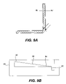
- FIGS. 8A and 8B a perspective view and cross section of the optically transparent member 10 are shown.
- the Figure shows the facets 14 sequentially numbered from one (1) through forty one (41).
- FIG. 8 b illustrates a cross section of the member 10 at line 8 b – 8 b ′ of FIG. 8A .
- the cross section 80 illustrates the facet 14 recessed within the side walls 18 of the member 10 .
- the cross section also shows the mirrored or reflective surface 82 of the facet 14 . By controlling the depth “d” of the reflective surface 82 of each of the facets 14 , the direction of the reflected light beams can be controlled.
- the depth (d) of the reflective surface 82 for the first (1), eighteenth (18) and thirtieth (30) facets 14 are 0.030, 0.084 and 0.188 mm respectively.
- the divergence of light emitted from the optically transparent member can be controlled by the height of the reflective surface 82 .
- the smaller the height of the reflective surface the broader or larger the divergence (i.e., same principle as a “single slit” diffraction) and vice versa.
- FIGS. 9A and 9B another perspective view and cross section of the member 10 is shown.
- FIG. 9B a cross section of the facet 14 along line 9 b – 9 b ′.
- the top surface 90 of the facet 14 is characterized by being taller in the vicinity 92 of the light emitting surface 93 and being shorter in the vicinity 94 of the reflective surface 82 .
- the height profile prevents the top surface of the facet 14 from blocking the light from the next facet 14 .
- the member 10 is made from a molded piece of plastic. In other embodiments, the member can be made from a machined or cut piece of glass or plastic.
- the shape or curvature of the reflective surface 82 of the facets 14 of member 10 can also be altered to achieve a desired optical result.
- the reflective surface 82 a is flat and at a 45 degree angle with regard to the side walls 18 (not shown) of the member 10 . Consequently, the reflected light, represented by arrows 102 a , are at 90 degrees.
- the reflective surface 82 b is shaped as a converging reflector. As a result, the reflected light beams 102 b converge at a focal point 104 b .
- the reflective surface 82 c is shaped as a diverging reflector.
- the reflected light beams 102 c therefore diverge in different directions.
- other reflective surfaces of member 10 e.g. the top, side or bottom surfaces of the member 10
- end surfaces, such as the ends of reflective surfaces 82 may be designed in a manner (e.g. curved or further angled) to direct the corresponding incident portion of the light striking such surfaces in a desired manner.
- any surface of the member 10 may be made reflective and oriented in a manner that directs the light. It should also be appreciated that the light may be reflected in a direction that falls within the plane of the member 10 or at an angle with that plane.
- any surface of the member 10 that light passes into our out of may be curved or otherwise oriented in a manner that refracts the light in a desired direction.
- This can include the light receiving end of member 10 , or any surface that light is arranged to pass out of. (e.g. the inner side wall, the top wall, the bottom wall, an end wall, etc. of the member 10 ).
- a collimating element 110 is shown integral with the light receiving end of the optically transparent member 10 .
- the collimating element 110 collimates the light from source 112 before it enters the input end of the optically transparent member 10 .
- the collimating element 110 can be integrally molded or cut from the same piece of plastic or glass used to make the member 10 .
- a beam splitter 122 is provided at the angle between the sides 10 a and 10 b of optically transparent member 10 .
- the beam splitter splits the light from light source 122 and directs the light down each side 10 a and 10 b.
- the present invention has been described with use with a two dimensional member 10 .
- the member 10 can be one dimensional, or more than two dimensions, for example three or more dimensions.
- the member 10 also can assume any shape (e.g., straight, curved, round, etc) and is not necessarily limited to L-shaped as described herein. can be used with either a one dimensional lamina plane (i.e., a line) or even a three dimensional lamina space (X axis, Y axis and Z axis).
- the number of light sources and light receiving arrays is generally, but not necessarily, the same as the number of axis used in the system.
- X axis and Y axis light sources 16 and 18 are used in the two dimensional lamina 12 illustrated in FIG. 1 .
- a single axis light source could be used to create the lamina.
- either internal or external reflective surfaces e.g., micro-mirrors
- the micro-mirrors can be flat, convergent, or divergent.
- Lenses or some other type of refractive element also can be placed on the light emitting surface of the side walls of the optically transparent member 10 .
- the refractive elements can be flat, convergent, or divergent. Therefore, the described embodiments should be taken as illustrative and not restrictive, and the invention should not be limited to the details given herein but should be defined by the following claims and their full scope of equivalents.
Abstract
Description
d n=1.875×10⁻⁴(n−1)2+0.030 mm (where n is the number of the facet)
For example, the depth (d) of the
Claims (37)
Priority Applications (1)
| Application Number | Priority Date | Filing Date | Title |
|---|---|---|---|
| US10/816,639 US7099553B1 (en) | 2003-04-08 | 2004-04-01 | Apparatus and method for generating a lamina of light |
Applications Claiming Priority (2)
| Application Number | Priority Date | Filing Date | Title |
|---|---|---|---|
| US46104703P | 2003-04-08 | 2003-04-08 | |
| US10/816,639 US7099553B1 (en) | 2003-04-08 | 2004-04-01 | Apparatus and method for generating a lamina of light |
Publications (1)
| Publication Number | Publication Date |
|---|---|
| US7099553B1 true US7099553B1 (en) | 2006-08-29 |
Family
ID=36915647
Family Applications (1)
| Application Number | Title | Priority Date | Filing Date |
|---|---|---|---|
| US10/816,639 Active 2024-11-10 US7099553B1 (en) | 2003-04-08 | 2004-04-01 | Apparatus and method for generating a lamina of light |
Country Status (1)
| Country | Link |
|---|---|
| US (1) | US7099553B1 (en) |
Cited By (50)
| Publication number | Priority date | Publication date | Assignee | Title |
|---|---|---|---|---|
| US20040201579A1 (en) * | 2003-04-08 | 2004-10-14 | Poa Sana, Inc., A California Corporation | Apparatus and method for a data input device using a light lamina screen and an optical position digitizer |
| US20050128190A1 (en) * | 2003-12-11 | 2005-06-16 | Nokia Corporation | Method and device for detecting touch pad input |
| US20050201681A1 (en) * | 2004-01-15 | 2005-09-15 | National Semiconductor Corporation | Hybrid waveguide |
| US20050271319A1 (en) * | 2004-06-04 | 2005-12-08 | National Semiconductor Corporation, A Delaware Corporation | Apparatus and method for a molded waveguide for use with touch screen displays |
| US20050271326A1 (en) * | 2004-06-04 | 2005-12-08 | National Semiconductor Corporation | Waveguide with a three-dimensional lens |
| US20050271983A1 (en) * | 2004-06-04 | 2005-12-08 | National Semiconductor Corporation | Techniques for manufacturing a waveguide with a three-dimensional lens |
| US20060114244A1 (en) * | 2004-11-30 | 2006-06-01 | Saxena Kuldeep K | Touch input system using light guides |
| US20070097097A1 (en) * | 2005-10-28 | 2007-05-03 | Jerry Liao | Laser type coordinate sensing system for touch module |
| US20070285406A1 (en) * | 2006-05-01 | 2007-12-13 | Rpo Pty Limited | Waveguide Materials for Optical Touch Screens |
| US20080013913A1 (en) * | 2006-07-12 | 2008-01-17 | Lumio | Optical touch screen |
| US20080031584A1 (en) * | 2006-08-02 | 2008-02-07 | National Semiconductor Corporation | Apparatus and method for a singulation of polymer waveguides using photolithography |
| US7333095B1 (en) * | 2006-07-12 | 2008-02-19 | Lumio Inc | Illumination for optical touch panel |
| US20080074402A1 (en) * | 2006-09-22 | 2008-03-27 | Rpo Pty Limited | Waveguide configurations for optical touch systems |
| WO2008038275A2 (en) * | 2006-09-28 | 2008-04-03 | Lumio Inc. | Optical touch panel |
| US7369724B2 (en) | 2006-10-03 | 2008-05-06 | National Semiconductor Corporation | Apparatus and method for an improved lens structure for polymer wave guides which maximizes free space light coupling |
| US20080106527A1 (en) * | 2006-11-06 | 2008-05-08 | Rpo Pty Limited | Waveguide Configurations for Minimising Substrate Area |
| US20080159694A1 (en) * | 2006-12-27 | 2008-07-03 | Rpo Pty Limited | Lens Configurations for Optical Touch Systems |
| US20080231604A1 (en) * | 2007-03-22 | 2008-09-25 | Cypress Semiconductor Corp. | Method for extending the life of touch screens |
| US20080266266A1 (en) * | 2007-04-25 | 2008-10-30 | Tyco Electronics Corporation | Touchscreen for detecting multiple touches |
| US20080273019A1 (en) * | 2007-05-02 | 2008-11-06 | National Semiconductor Corporation | Shadow detection in optical touch sensor through the linear combination of optical beams and grey-scale determination of detected shadow edges |
| US20080278460A1 (en) * | 2007-05-11 | 2008-11-13 | Rpo Pty Limited | Transmissive Body |
| US20090141002A1 (en) * | 2007-12-03 | 2009-06-04 | Lg Display Co., Ltd. | Touch panel display device |
| US20090141005A1 (en) * | 2007-11-29 | 2009-06-04 | Nitto Denko Corporation | Optical waveguide for touch panel and touch panel using the same |
| WO2009086836A1 (en) * | 2008-01-11 | 2009-07-16 | Danmarks Tekniske Universitet | A touch-sensitive device |
| US20090200453A1 (en) * | 2008-02-07 | 2009-08-13 | Lumio Inc. | Optical Touch Screen Assembly |
| US20090237375A1 (en) * | 2008-03-24 | 2009-09-24 | Nitto Denko Corporation | Apparatus using waveguide, optical touch panel, and method of fabricating waveguide |
| US20090262097A1 (en) * | 2008-04-17 | 2009-10-22 | Jung-Yu Chen | Frame assembly for touch screen |
| US20100128006A1 (en) * | 2008-11-26 | 2010-05-27 | Nitto Denko Corporation | Optical waveguide and optical touch panel |
| US20100214269A1 (en) * | 2009-02-25 | 2010-08-26 | Pixart Imaging Inc. | Optical touch module |
| US20100253637A1 (en) * | 2009-04-07 | 2010-10-07 | Lumio | Drift Compensated Optical Touch Screen |
| CN101901082A (en) * | 2009-06-01 | 2010-12-01 | 北京汇冠新技术股份有限公司 | Touch detection device |
| US20100309169A1 (en) * | 2009-06-03 | 2010-12-09 | Lumio Inc. | Optical Touch Screen with Reflectors |
| US20100315380A1 (en) * | 2009-06-16 | 2010-12-16 | Raydium Semiconductor Corporation | Optical touch apparatus and operating method thereof |
| US20110012868A1 (en) * | 2009-07-16 | 2011-01-20 | Raydium Semiconductor Corporation | Optical touch apparatus and operating method thereof |
| US20110063334A1 (en) * | 2009-08-21 | 2011-03-17 | Advanced Display Technology Ag | Display Element and a Method for Driving a Display Element |
| US20110115720A1 (en) * | 2009-11-19 | 2011-05-19 | Garmin International, Inc. | Optical overlay for an electronic display |
| JP2011253095A (en) * | 2010-06-03 | 2011-12-15 | Nitto Denko Corp | L-shaped optical waveguide device |
| US20120013577A1 (en) * | 2010-07-15 | 2012-01-19 | Quanta Computer Inc. | Optical touch structure |
| US20120218226A1 (en) * | 2011-02-28 | 2012-08-30 | Hon Hai Precision Industry Co., Ltd. | Light directing element and infrared touch screen device having same |
| JP2013522801A (en) * | 2010-03-24 | 2013-06-13 | ネオノード インコーポレイテッド | Lens array for light-based touch screen |
| CN103376497A (en) * | 2012-04-20 | 2013-10-30 | 纬创资通股份有限公司 | Illumination module and display device |
| US8674966B2 (en) | 2001-11-02 | 2014-03-18 | Neonode Inc. | ASIC controller for light-based touch screen |
| US20140181964A1 (en) * | 2012-12-24 | 2014-06-26 | Samsung Electronics Co., Ltd. | Method for managing security for applications and an electronic device thereof |
| US9052777B2 (en) | 2001-11-02 | 2015-06-09 | Neonode Inc. | Optical elements with alternating reflective lens facets |
| US20160026269A1 (en) * | 2012-02-10 | 2016-01-28 | ISIOIRI INTERFACE TECHNOLOGIES GnbH | Device for entering information into a data processing system |
| WO2016029376A1 (en) * | 2014-08-27 | 2016-03-03 | Hewlett-Packard Development Company, L.P. | Screen contact detection using total internal reflection |
| US9453968B2 (en) | 2013-08-01 | 2016-09-27 | Albert M. David | Optical touch sensing apparatus and method using distributed band pass filter |
| US9778794B2 (en) | 2001-11-02 | 2017-10-03 | Neonode Inc. | Light-based touch screen |
| US11669210B2 (en) | 2020-09-30 | 2023-06-06 | Neonode Inc. | Optical touch sensor |
| US11886001B2 (en) * | 2019-12-20 | 2024-01-30 | Snap Inc. | Optical waveguide fabrication process |
Citations (15)
| Publication number | Priority date | Publication date | Assignee | Title |
|---|---|---|---|---|
| US3584226A (en) * | 1969-04-14 | 1971-06-08 | Automated Packaging Syst Inc | Counting system |
| US4068121A (en) * | 1976-05-17 | 1978-01-10 | Tally Corporation | Light collector and prism light source for photoelectric readers |
| US4737626A (en) * | 1985-02-15 | 1988-04-12 | Alps Electric Co., Ltd. | Photoelectric touch panel having reflector and transparent photoconductive plate |
| US4746770A (en) | 1987-02-17 | 1988-05-24 | Sensor Frame Incorporated | Method and apparatus for isolating and manipulating graphic objects on computer video monitor |
| US4776661A (en) * | 1985-11-25 | 1988-10-11 | Canon Kabushiki Kaisha | Integrated optical device |
| US5050946A (en) * | 1990-09-27 | 1991-09-24 | Compaq Computer Corporation | Faceted light pipe |
| US5235193A (en) * | 1990-11-13 | 1993-08-10 | Hoffman-La Roche Inc. | Device for identifying a container carrier for an automatic analytical apparatus with faceted light guiding plate |
| US5414413A (en) | 1988-06-14 | 1995-05-09 | Sony Corporation | Touch panel apparatus |
| US5512943A (en) * | 1994-04-14 | 1996-04-30 | Arriflex Corporation | Video monitor contrast reference gray scale apparatus and method of use thereof |
| US5668913A (en) * | 1994-10-19 | 1997-09-16 | Tai; Ping-Kaung | Light expanding system for producing a linear or planar light beam from a point-like light source |
| US5786810A (en) * | 1995-06-07 | 1998-07-28 | Compaq Computer Corporation | Method of determining an object's position and associated apparatus |
| US5914709A (en) | 1997-03-14 | 1999-06-22 | Poa Sana, Llc | User input device for a computer system |
| US6181842B1 (en) | 2000-01-10 | 2001-01-30 | Poa Sana, Inc. | Position digitizer waveguide array with integrated collimating optics |
| US6525677B1 (en) * | 2000-08-28 | 2003-02-25 | Motorola, Inc. | Method and apparatus for an optical laser keypad |
| US6734929B2 (en) * | 2002-02-05 | 2004-05-11 | Alps Electric Co., Ltd. | Illumination device having a single light source and liquid crystal display device |
-
2004
- 2004-04-01 US US10/816,639 patent/US7099553B1/en active Active
Patent Citations (16)
| Publication number | Priority date | Publication date | Assignee | Title |
|---|---|---|---|---|
| US3584226A (en) * | 1969-04-14 | 1971-06-08 | Automated Packaging Syst Inc | Counting system |
| US4068121A (en) * | 1976-05-17 | 1978-01-10 | Tally Corporation | Light collector and prism light source for photoelectric readers |
| US4737626A (en) * | 1985-02-15 | 1988-04-12 | Alps Electric Co., Ltd. | Photoelectric touch panel having reflector and transparent photoconductive plate |
| US4776661A (en) * | 1985-11-25 | 1988-10-11 | Canon Kabushiki Kaisha | Integrated optical device |
| US4746770A (en) | 1987-02-17 | 1988-05-24 | Sensor Frame Incorporated | Method and apparatus for isolating and manipulating graphic objects on computer video monitor |
| US5414413A (en) | 1988-06-14 | 1995-05-09 | Sony Corporation | Touch panel apparatus |
| US5050946A (en) * | 1990-09-27 | 1991-09-24 | Compaq Computer Corporation | Faceted light pipe |
| US5235193A (en) * | 1990-11-13 | 1993-08-10 | Hoffman-La Roche Inc. | Device for identifying a container carrier for an automatic analytical apparatus with faceted light guiding plate |
| US5512943A (en) * | 1994-04-14 | 1996-04-30 | Arriflex Corporation | Video monitor contrast reference gray scale apparatus and method of use thereof |
| US5668913A (en) * | 1994-10-19 | 1997-09-16 | Tai; Ping-Kaung | Light expanding system for producing a linear or planar light beam from a point-like light source |
| US5786810A (en) * | 1995-06-07 | 1998-07-28 | Compaq Computer Corporation | Method of determining an object's position and associated apparatus |
| US5914709A (en) | 1997-03-14 | 1999-06-22 | Poa Sana, Llc | User input device for a computer system |
| US6351260B1 (en) | 1997-03-14 | 2002-02-26 | Poa Sana, Inc. | User input device for a computer system |
| US6181842B1 (en) | 2000-01-10 | 2001-01-30 | Poa Sana, Inc. | Position digitizer waveguide array with integrated collimating optics |
| US6525677B1 (en) * | 2000-08-28 | 2003-02-25 | Motorola, Inc. | Method and apparatus for an optical laser keypad |
| US6734929B2 (en) * | 2002-02-05 | 2004-05-11 | Alps Electric Co., Ltd. | Illumination device having a single light source and liquid crystal display device |
Cited By (100)
| Publication number | Priority date | Publication date | Assignee | Title |
|---|---|---|---|---|
| US9052777B2 (en) | 2001-11-02 | 2015-06-09 | Neonode Inc. | Optical elements with alternating reflective lens facets |
| US9035917B2 (en) | 2001-11-02 | 2015-05-19 | Neonode Inc. | ASIC controller for light-based sensor |
| US9778794B2 (en) | 2001-11-02 | 2017-10-03 | Neonode Inc. | Light-based touch screen |
| US8674966B2 (en) | 2001-11-02 | 2014-03-18 | Neonode Inc. | ASIC controller for light-based touch screen |
| US20040201579A1 (en) * | 2003-04-08 | 2004-10-14 | Poa Sana, Inc., A California Corporation | Apparatus and method for a data input device using a light lamina screen and an optical position digitizer |
| US7786983B2 (en) * | 2003-04-08 | 2010-08-31 | Poa Sana Liquidating Trust | Apparatus and method for a data input device using a light lamina screen |
| US7265748B2 (en) * | 2003-12-11 | 2007-09-04 | Nokia Corporation | Method and device for detecting touch pad input |
| US20050128190A1 (en) * | 2003-12-11 | 2005-06-16 | Nokia Corporation | Method and device for detecting touch pad input |
| US7509011B2 (en) | 2004-01-15 | 2009-03-24 | Poa Sana Liquidating Trust | Hybrid waveguide |
| US20050201681A1 (en) * | 2004-01-15 | 2005-09-15 | National Semiconductor Corporation | Hybrid waveguide |
| US7474816B2 (en) | 2004-06-04 | 2009-01-06 | Poa Sana Liquidating Trust | Waveguide with a three dimensional lens |
| US7267930B2 (en) | 2004-06-04 | 2007-09-11 | National Semiconductor Corporation | Techniques for manufacturing a waveguide with a three-dimensional lens |
| US20050271319A1 (en) * | 2004-06-04 | 2005-12-08 | National Semiconductor Corporation, A Delaware Corporation | Apparatus and method for a molded waveguide for use with touch screen displays |
| US7471865B2 (en) | 2004-06-04 | 2008-12-30 | Poa Sana Liquidating Trust | Apparatus and method for a molded waveguide for use with touch screen displays |
| US7676131B2 (en) | 2004-06-04 | 2010-03-09 | Poa Sana Liquidating Trust | Waveguide with a three-dimensional lens |
| US20070189668A1 (en) * | 2004-06-04 | 2007-08-16 | National Semiconductor Corporation | Techniques for manufacturing a waveguide with a three dimensional lens |
| US20050271983A1 (en) * | 2004-06-04 | 2005-12-08 | National Semiconductor Corporation | Techniques for manufacturing a waveguide with a three-dimensional lens |
| US7520050B2 (en) | 2004-06-04 | 2009-04-21 | Poasana Liquidating Trust | Apparatus and method for a molded waveguide for use with touch screen displays |
| US20050271326A1 (en) * | 2004-06-04 | 2005-12-08 | National Semiconductor Corporation | Waveguide with a three-dimensional lens |
| US20060114244A1 (en) * | 2004-11-30 | 2006-06-01 | Saxena Kuldeep K | Touch input system using light guides |
| US8130210B2 (en) * | 2004-11-30 | 2012-03-06 | Avago Technologies Ecbu Ip (Singapore) Pte. Ltd. | Touch input system using light guides |
| US20070097097A1 (en) * | 2005-10-28 | 2007-05-03 | Jerry Liao | Laser type coordinate sensing system for touch module |
| US8120595B2 (en) | 2006-05-01 | 2012-02-21 | Rpo Pty Limited | Waveguide materials for optical touch screens |
| US20070285406A1 (en) * | 2006-05-01 | 2007-12-13 | Rpo Pty Limited | Waveguide Materials for Optical Touch Screens |
| US20080093542A1 (en) * | 2006-07-12 | 2008-04-24 | Lumio Inc. | Device and Method for Optical Touch Panel Illumination |
| US20080013913A1 (en) * | 2006-07-12 | 2008-01-17 | Lumio | Optical touch screen |
| US7333094B2 (en) | 2006-07-12 | 2008-02-19 | Lumio Inc. | Optical touch screen |
| US7573465B2 (en) * | 2006-07-12 | 2009-08-11 | Lumio Inc | Optical touch panel |
| US7477241B2 (en) | 2006-07-12 | 2009-01-13 | Lumio Inc. | Device and method for optical touch panel illumination |
| US20080068353A1 (en) * | 2006-07-12 | 2008-03-20 | Lumio | Optical Touch Panel |
| US7333095B1 (en) * | 2006-07-12 | 2008-02-19 | Lumio Inc | Illumination for optical touch panel |
| US20080047762A1 (en) * | 2006-07-12 | 2008-02-28 | Lumio Inc. | Illumination for optical touch panel |
| US20080031584A1 (en) * | 2006-08-02 | 2008-02-07 | National Semiconductor Corporation | Apparatus and method for a singulation of polymer waveguides using photolithography |
| US8674963B2 (en) | 2006-09-22 | 2014-03-18 | Zetta Research and Development LLC—RPO Series | Waveguide configurations for optical touch systems |
| US20080074402A1 (en) * | 2006-09-22 | 2008-03-27 | Rpo Pty Limited | Waveguide configurations for optical touch systems |
| WO2008038275A2 (en) * | 2006-09-28 | 2008-04-03 | Lumio Inc. | Optical touch panel |
| WO2008038275A3 (en) * | 2006-09-28 | 2009-04-23 | Lumio Inc | Optical touch panel |
| US7369724B2 (en) | 2006-10-03 | 2008-05-06 | National Semiconductor Corporation | Apparatus and method for an improved lens structure for polymer wave guides which maximizes free space light coupling |
| US20080106527A1 (en) * | 2006-11-06 | 2008-05-08 | Rpo Pty Limited | Waveguide Configurations for Minimising Substrate Area |
| US20080159694A1 (en) * | 2006-12-27 | 2008-07-03 | Rpo Pty Limited | Lens Configurations for Optical Touch Systems |
| US20080231604A1 (en) * | 2007-03-22 | 2008-09-25 | Cypress Semiconductor Corp. | Method for extending the life of touch screens |
| TWI417765B (en) * | 2007-04-25 | 2013-12-01 | Elo Touch Solutions Inc | A touchscreen for detecting multiple touches |
| US8243048B2 (en) | 2007-04-25 | 2012-08-14 | Elo Touch Solutions, Inc. | Touchscreen for detecting multiple touches |
| US10289250B2 (en) * | 2007-04-25 | 2019-05-14 | Elo Touch Solutions, Inc. | Touchscreen for detecting multiple touches |
| US20080266266A1 (en) * | 2007-04-25 | 2008-10-30 | Tyco Electronics Corporation | Touchscreen for detecting multiple touches |
| EP2804080A3 (en) * | 2007-04-25 | 2014-12-24 | Elo Touch Solutions, Inc. | A touchscreen for detecting multiple touches |
| US20170052646A1 (en) * | 2007-04-25 | 2017-02-23 | Elo Touch Solutions, Inc. | Touchscreen for Detecting Multiple Touches |
| US9454266B2 (en) | 2007-04-25 | 2016-09-27 | Elo Touch Solutions, Inc. | Touchscreen for detecting multiple touches |
| US20080273019A1 (en) * | 2007-05-02 | 2008-11-06 | National Semiconductor Corporation | Shadow detection in optical touch sensor through the linear combination of optical beams and grey-scale determination of detected shadow edges |
| US7809221B2 (en) | 2007-05-02 | 2010-10-05 | Poa Sana Liquidating Trust | Shadow detection in optical touch sensor through the linear combination of optical beams and grey-scale determination of detected shadow edges |
| US20080278460A1 (en) * | 2007-05-11 | 2008-11-13 | Rpo Pty Limited | Transmissive Body |
| US8842366B2 (en) * | 2007-05-11 | 2014-09-23 | Zetta Research and Development LLC—RPO Series | Transmissive body |
| US20090141005A1 (en) * | 2007-11-29 | 2009-06-04 | Nitto Denko Corporation | Optical waveguide for touch panel and touch panel using the same |
| US7941016B2 (en) * | 2007-11-29 | 2011-05-10 | Nitto Denko Corporation | Optical waveguide for touch panel and touch panel using the same |
| GB2455385B (en) * | 2007-12-03 | 2011-12-28 | Lg Display Co Ltd | Touch panel display device |
| US8581882B2 (en) | 2007-12-03 | 2013-11-12 | Lg Display Co., Ltd. | Touch panel display device |
| US20090141002A1 (en) * | 2007-12-03 | 2009-06-04 | Lg Display Co., Ltd. | Touch panel display device |
| CN101452358B (en) * | 2007-12-03 | 2011-01-26 | 乐金显示有限公司 | Contact panel display |
| US9740336B2 (en) | 2008-01-11 | 2017-08-22 | O-Net Wavetouch Limited | Touch-sensitive device |
| US20110025620A1 (en) * | 2008-01-11 | 2011-02-03 | Opdi Technologies A/S | Touch-sensitive device |
| US9342187B2 (en) | 2008-01-11 | 2016-05-17 | O-Net Wavetouch Limited | Touch-sensitive device |
| JP2014017000A (en) * | 2008-01-11 | 2014-01-30 | O-Net Wavetouch Limited | Touch-sensitive device |
| WO2009086836A1 (en) * | 2008-01-11 | 2009-07-16 | Danmarks Tekniske Universitet | A touch-sensitive device |
| US20090200453A1 (en) * | 2008-02-07 | 2009-08-13 | Lumio Inc. | Optical Touch Screen Assembly |
| US7781722B2 (en) | 2008-02-07 | 2010-08-24 | Lumio Inc | Optical touch screen assembly |
| US20090237375A1 (en) * | 2008-03-24 | 2009-09-24 | Nitto Denko Corporation | Apparatus using waveguide, optical touch panel, and method of fabricating waveguide |
| US8200051B2 (en) | 2008-03-24 | 2012-06-12 | Nitto Denko Corporation | Apparatus using waveguide, optical touch panel, and method of fabricating waveguide |
| US7995042B2 (en) * | 2008-04-17 | 2011-08-09 | Et&T Technology Co., Ltd. | Frame assembly for touch screen |
| US20090262097A1 (en) * | 2008-04-17 | 2009-10-22 | Jung-Yu Chen | Frame assembly for touch screen |
| US20100128006A1 (en) * | 2008-11-26 | 2010-05-27 | Nitto Denko Corporation | Optical waveguide and optical touch panel |
| US8009944B2 (en) * | 2008-11-26 | 2011-08-30 | Nitto Denko Corporation | Optical waveguide and optical touch panel |
| US20100214269A1 (en) * | 2009-02-25 | 2010-08-26 | Pixart Imaging Inc. | Optical touch module |
| US8502803B2 (en) | 2009-04-07 | 2013-08-06 | Lumio Inc | Drift compensated optical touch screen |
| US20100253637A1 (en) * | 2009-04-07 | 2010-10-07 | Lumio | Drift Compensated Optical Touch Screen |
| CN101901082A (en) * | 2009-06-01 | 2010-12-01 | 北京汇冠新技术股份有限公司 | Touch detection device |
| EP2259173A3 (en) * | 2009-06-01 | 2014-07-16 | Beijing Irtouch Systems Co., Ltd. | Touch detection apparatus |
| US20100309169A1 (en) * | 2009-06-03 | 2010-12-09 | Lumio Inc. | Optical Touch Screen with Reflectors |
| US20100315380A1 (en) * | 2009-06-16 | 2010-12-16 | Raydium Semiconductor Corporation | Optical touch apparatus and operating method thereof |
| US8698780B2 (en) * | 2009-06-16 | 2014-04-15 | Raydium Semiconductor Corporation | Optical touch apparatus with noise suppressing function and method of operating the same |
| US8593435B2 (en) * | 2009-07-16 | 2013-11-26 | Raydium Semiconductor Corporation | Optical touch apparatus with high resolution and method of operating the same |
| US20110012868A1 (en) * | 2009-07-16 | 2011-01-20 | Raydium Semiconductor Corporation | Optical touch apparatus and operating method thereof |
| US20110063334A1 (en) * | 2009-08-21 | 2011-03-17 | Advanced Display Technology Ag | Display Element and a Method for Driving a Display Element |
| US8547406B2 (en) * | 2009-08-21 | 2013-10-01 | Advanced Display Technology Ag | Display element and a method for driving a display element |
| US20110115720A1 (en) * | 2009-11-19 | 2011-05-19 | Garmin International, Inc. | Optical overlay for an electronic display |
| US8330736B2 (en) * | 2009-11-19 | 2012-12-11 | Garmin International, Inc. | Optical overlay for an electronic display |
| JP2013522801A (en) * | 2010-03-24 | 2013-06-13 | ネオノード インコーポレイテッド | Lens array for light-based touch screen |
| JP2011253095A (en) * | 2010-06-03 | 2011-12-15 | Nitto Denko Corp | L-shaped optical waveguide device |
| US20120013577A1 (en) * | 2010-07-15 | 2012-01-19 | Quanta Computer Inc. | Optical touch structure |
| US8890845B2 (en) * | 2010-07-15 | 2014-11-18 | Quanta Computer Inc. | Optical touch screen |
| US20120218226A1 (en) * | 2011-02-28 | 2012-08-30 | Hon Hai Precision Industry Co., Ltd. | Light directing element and infrared touch screen device having same |
| US20160026269A1 (en) * | 2012-02-10 | 2016-01-28 | ISIOIRI INTERFACE TECHNOLOGIES GnbH | Device for entering information into a data processing system |
| US8967847B2 (en) * | 2012-04-20 | 2015-03-03 | Wistron Corporation | Illumination assembly and display module |
| CN103376497B (en) * | 2012-04-20 | 2016-08-03 | 纬创资通股份有限公司 | Illumination module and display device |
| CN103376497A (en) * | 2012-04-20 | 2013-10-30 | 纬创资通股份有限公司 | Illumination module and display device |
| US20140181964A1 (en) * | 2012-12-24 | 2014-06-26 | Samsung Electronics Co., Ltd. | Method for managing security for applications and an electronic device thereof |
| US9453968B2 (en) | 2013-08-01 | 2016-09-27 | Albert M. David | Optical touch sensing apparatus and method using distributed band pass filter |
| WO2016029376A1 (en) * | 2014-08-27 | 2016-03-03 | Hewlett-Packard Development Company, L.P. | Screen contact detection using total internal reflection |
| US10423281B2 (en) | 2014-08-27 | 2019-09-24 | Hewlett-Packard Development Company, L.P. | Screen contact detection using total internal reflection |
| US11886001B2 (en) * | 2019-12-20 | 2024-01-30 | Snap Inc. | Optical waveguide fabrication process |
| US11669210B2 (en) | 2020-09-30 | 2023-06-06 | Neonode Inc. | Optical touch sensor |
Similar Documents
| Publication | Publication Date | Title |
|---|---|---|
| US7099553B1 (en) | Apparatus and method for generating a lamina of light | |
| US10289250B2 (en) | Touchscreen for detecting multiple touches | |
| US8184108B2 (en) | Apparatus and method for a folded optical element waveguide for use with light based touch screens | |
| US8842366B2 (en) | Transmissive body | |
| US20120098794A1 (en) | Transmissive Body | |
| JP5949931B2 (en) | Optical sensor | |
| US20150070327A1 (en) | Optical touch panel and touchscreen | |
| US10473928B2 (en) | Backlight unit and head-up display device | |
| US20080007542A1 (en) | Optical touchpad with three-dimensional position determination | |
| KR20200088313A (en) | Thin-film coupler and reflector of sensing waveguide | |
| KR20180037749A (en) | Display apparatus | |
| US9128250B2 (en) | Optical systems for infrared touch screens | |
| KR20120058522A (en) | Scanning collimation of light via flat panel lamp | |
| US20200133012A1 (en) | Optical element and optical system | |
| US9170684B2 (en) | Optical navigation device | |
| US11215874B2 (en) | Light collimation device, backlight module and display panel | |
| KR20200029329A (en) | Illumination device and electronic apparatus including the same and a method of illuminating | |
| WO2024075599A1 (en) | Light irradiation device, optical ranging device, and vehicle |
Legal Events
| Date | Code | Title | Description |
|---|---|---|---|
| AS | Assignment |
Owner name: POA SANA, INC., CALIFORNIA Free format text: ASSIGNMENT OF ASSIGNORS INTEREST;ASSIGNORS:GRAHAM, DAVID S.;MA, GUOLIN;SCHLEUNING, DAVID;AND OTHERS;REEL/FRAME:015076/0364;SIGNING DATES FROM 20040713 TO 20040809 |
|
| STCF | Information on status: patent grant |
Free format text: PATENTED CASE |
|
| AS | Assignment |
Owner name: POA SANA LIQUIDATING TRUST, CALIFORNIA Free format text: ASSIGNMENT OF ASSIGNORS INTEREST;ASSIGNOR:POA SANA, INC.;REEL/FRAME:023607/0545 Effective date: 20061001 |
|
| FPAY | Fee payment |
Year of fee payment: 4 |
|
| FPAY | Fee payment |
Year of fee payment: 8 |
|
| MAFP | Maintenance fee payment |
Free format text: PAYMENT OF MAINTENANCE FEE, 12TH YEAR, LARGE ENTITY (ORIGINAL EVENT CODE: M1553) Year of fee payment: 12 |