US7074654B1 - Tape supported memory card leadframe structure - Google Patents
Tape supported memory card leadframe structure Download PDFInfo
- Publication number
- US7074654B1 US7074654B1 US10/828,616 US82861604A US7074654B1 US 7074654 B1 US7074654 B1 US 7074654B1 US 82861604 A US82861604 A US 82861604A US 7074654 B1 US7074654 B1 US 7074654B1
- Authority
- US
- United States
- Prior art keywords
- leadframe
- dambar
- contacts
- tape
- die pad
- Prior art date
- Legal status (The legal status is an assumption and is not a legal conclusion. Google has not performed a legal analysis and makes no representation as to the accuracy of the status listed.)
- Active, expires
Links
Images


Classifications
-
- H—ELECTRICITY
- H01—ELECTRIC ELEMENTS
- H01L—SEMICONDUCTOR DEVICES NOT COVERED BY CLASS H10
- H01L23/00—Details of semiconductor or other solid state devices
- H01L23/48—Arrangements for conducting electric current to or from the solid state body in operation, e.g. leads, terminal arrangements ; Selection of materials therefor
- H01L23/488—Arrangements for conducting electric current to or from the solid state body in operation, e.g. leads, terminal arrangements ; Selection of materials therefor consisting of soldered or bonded constructions
- H01L23/495—Lead-frames or other flat leads
- H01L23/49541—Geometry of the lead-frame
- H01L23/49558—Insulating layers on lead frames, e.g. bridging members
-
- G—PHYSICS
- G06—COMPUTING; CALCULATING OR COUNTING
- G06K—GRAPHICAL DATA READING; PRESENTATION OF DATA; RECORD CARRIERS; HANDLING RECORD CARRIERS
- G06K19/00—Record carriers for use with machines and with at least a part designed to carry digital markings
- G06K19/06—Record carriers for use with machines and with at least a part designed to carry digital markings characterised by the kind of the digital marking, e.g. shape, nature, code
- G06K19/067—Record carriers with conductive marks, printed circuits or semiconductor circuit elements, e.g. credit or identity cards also with resonating or responding marks without active components
- G06K19/07—Record carriers with conductive marks, printed circuits or semiconductor circuit elements, e.g. credit or identity cards also with resonating or responding marks without active components with integrated circuit chips
- G06K19/077—Constructional details, e.g. mounting of circuits in the carrier
- G06K19/0772—Physical layout of the record carrier
- G06K19/07732—Physical layout of the record carrier the record carrier having a housing or construction similar to well-known portable memory devices, such as SD cards, USB or memory sticks
-
- H—ELECTRICITY
- H01—ELECTRIC ELEMENTS
- H01L—SEMICONDUCTOR DEVICES NOT COVERED BY CLASS H10
- H01L23/00—Details of semiconductor or other solid state devices
- H01L23/28—Encapsulations, e.g. encapsulating layers, coatings, e.g. for protection
- H01L23/31—Encapsulations, e.g. encapsulating layers, coatings, e.g. for protection characterised by the arrangement or shape
- H01L23/3107—Encapsulations, e.g. encapsulating layers, coatings, e.g. for protection characterised by the arrangement or shape the device being completely enclosed
-
- H—ELECTRICITY
- H01—ELECTRIC ELEMENTS
- H01L—SEMICONDUCTOR DEVICES NOT COVERED BY CLASS H10
- H01L2224/00—Indexing scheme for arrangements for connecting or disconnecting semiconductor or solid-state bodies and methods related thereto as covered by H01L24/00
- H01L2224/01—Means for bonding being attached to, or being formed on, the surface to be connected, e.g. chip-to-package, die-attach, "first-level" interconnects; Manufacturing methods related thereto
- H01L2224/42—Wire connectors; Manufacturing methods related thereto
- H01L2224/47—Structure, shape, material or disposition of the wire connectors after the connecting process
- H01L2224/48—Structure, shape, material or disposition of the wire connectors after the connecting process of an individual wire connector
- H01L2224/4805—Shape
- H01L2224/4809—Loop shape
- H01L2224/48091—Arched
-
- H—ELECTRICITY
- H01—ELECTRIC ELEMENTS
- H01L—SEMICONDUCTOR DEVICES NOT COVERED BY CLASS H10
- H01L2224/00—Indexing scheme for arrangements for connecting or disconnecting semiconductor or solid-state bodies and methods related thereto as covered by H01L24/00
- H01L2224/01—Means for bonding being attached to, or being formed on, the surface to be connected, e.g. chip-to-package, die-attach, "first-level" interconnects; Manufacturing methods related thereto
- H01L2224/42—Wire connectors; Manufacturing methods related thereto
- H01L2224/47—Structure, shape, material or disposition of the wire connectors after the connecting process
- H01L2224/48—Structure, shape, material or disposition of the wire connectors after the connecting process of an individual wire connector
- H01L2224/481—Disposition
- H01L2224/48135—Connecting between different semiconductor or solid-state bodies, i.e. chip-to-chip
- H01L2224/48145—Connecting between different semiconductor or solid-state bodies, i.e. chip-to-chip the bodies being stacked
- H01L2224/48147—Connecting between different semiconductor or solid-state bodies, i.e. chip-to-chip the bodies being stacked with an intermediate bond, e.g. continuous wire daisy chain
-
- H—ELECTRICITY
- H01—ELECTRIC ELEMENTS
- H01L—SEMICONDUCTOR DEVICES NOT COVERED BY CLASS H10
- H01L2224/00—Indexing scheme for arrangements for connecting or disconnecting semiconductor or solid-state bodies and methods related thereto as covered by H01L24/00
- H01L2224/01—Means for bonding being attached to, or being formed on, the surface to be connected, e.g. chip-to-package, die-attach, "first-level" interconnects; Manufacturing methods related thereto
- H01L2224/42—Wire connectors; Manufacturing methods related thereto
- H01L2224/47—Structure, shape, material or disposition of the wire connectors after the connecting process
- H01L2224/49—Structure, shape, material or disposition of the wire connectors after the connecting process of a plurality of wire connectors
- H01L2224/491—Disposition
- H01L2224/4911—Disposition the connectors being bonded to at least one common bonding area, e.g. daisy chain
-
- H—ELECTRICITY
- H01—ELECTRIC ELEMENTS
- H01L—SEMICONDUCTOR DEVICES NOT COVERED BY CLASS H10
- H01L24/00—Arrangements for connecting or disconnecting semiconductor or solid-state bodies; Methods or apparatus related thereto
- H01L24/01—Means for bonding being attached to, or being formed on, the surface to be connected, e.g. chip-to-package, die-attach, "first-level" interconnects; Manufacturing methods related thereto
- H01L24/42—Wire connectors; Manufacturing methods related thereto
- H01L24/47—Structure, shape, material or disposition of the wire connectors after the connecting process
- H01L24/48—Structure, shape, material or disposition of the wire connectors after the connecting process of an individual wire connector
-
- H—ELECTRICITY
- H01—ELECTRIC ELEMENTS
- H01L—SEMICONDUCTOR DEVICES NOT COVERED BY CLASS H10
- H01L24/00—Arrangements for connecting or disconnecting semiconductor or solid-state bodies; Methods or apparatus related thereto
- H01L24/01—Means for bonding being attached to, or being formed on, the surface to be connected, e.g. chip-to-package, die-attach, "first-level" interconnects; Manufacturing methods related thereto
- H01L24/42—Wire connectors; Manufacturing methods related thereto
- H01L24/47—Structure, shape, material or disposition of the wire connectors after the connecting process
- H01L24/49—Structure, shape, material or disposition of the wire connectors after the connecting process of a plurality of wire connectors
-
- H—ELECTRICITY
- H01—ELECTRIC ELEMENTS
- H01L—SEMICONDUCTOR DEVICES NOT COVERED BY CLASS H10
- H01L2924/00—Indexing scheme for arrangements or methods for connecting or disconnecting semiconductor or solid-state bodies as covered by H01L24/00
- H01L2924/0001—Technical content checked by a classifier
- H01L2924/00014—Technical content checked by a classifier the subject-matter covered by the group, the symbol of which is combined with the symbol of this group, being disclosed without further technical details
-
- H—ELECTRICITY
- H01—ELECTRIC ELEMENTS
- H01L—SEMICONDUCTOR DEVICES NOT COVERED BY CLASS H10
- H01L2924/00—Indexing scheme for arrangements or methods for connecting or disconnecting semiconductor or solid-state bodies as covered by H01L24/00
- H01L2924/10—Details of semiconductor or other solid state devices to be connected
- H01L2924/11—Device type
- H01L2924/14—Integrated circuits
Definitions
- the present invention relates generally to memory cards, and more particularly, to a memory card (e.g., a multi-media card (MMC)) wherein tape or an epoxy is used to support the external signal contacts (ESC's) of the memory card leadframe structure so that the tie bars used to connect the contacts to the outer frame of the leadframe can be removed prior to the molding of the package body of the memory card.
- MMC multi-media card
- memory cards are being used in increasing numbers to provide memory storage and other electronic functions for devices such as digital cameras, MP3 players, cellular phones, and Personal Digital Assistants.
- memory cards are provided in various formats, including multi-media cards and secure digital cards.
- memory cards comprise multiple integrated circuit devices or semiconductor dies.
- the dies are interconnected using a circuit board substrate which adds to the weight, thickness, stiffness and complexity of the card.
- Memory cards also include electrical contacts for providing an external interface to an insertion point or socket. These electrical contacts are typically disposed on the backside of the circuit board substrate, with the electrical connection to the dies being provided by vias which extend through the circuit board substrate.
- the body is sized and configured to meet or achieve a “form factor” for the memory card.
- the contacts of the leadframe are exposed within a common surface of the body, with the die pad of the leadframe and the semiconductor die mounted thereto being disposed within or covered by the body.
- Memory cards such as multi-media cards, are used by advancing the same into a host socket which includes a plurality of connector pins.
- Many host sockets include nine connector pins to accommodate the seven contacts included in many memory card formats such as multi-media cards, and the nine contacts included in the secure digital card memory card format.
- Applicant has previously determined that one of the drawbacks associated with leadframe based memory cards is that portions of the tie bars which are used to connect the contacts to the outer frame of the leadframe are typically exposed in the leading edge of the memory card which is initially advanced into the host socket.
- tie bars exposed within this leading edge are the severed ends of the tie bars created as a result of the cutting or singulation process typically used to separate the outer frame of the leadframe from the remainder thereof subsequent to the formation of the body of the memory card.
- These exposed portions of the tie bars give rise to a potential to short against the metal features of the host socket, and are thus highly undesirable.
- the present invention addresses and overcomes the above-described deficiencies of currently known leadframe based memory cards by providing a memory card wherein tape or an epoxy is used to support the contacts of the memory card leadframe structure so that the tie bars used to secure the contacts to the outer frame can be removed prior to the molding of the body of the memory card. More particularly, the tape or epoxy is applied to the leadframe, with the tie bars thereafter being punched out or otherwise removed, thus leaving the tape or epoxy to hold the contacts of the leadframe structure in place during the remaining steps of the assembly process.
- a method for manufacturing a memory card such as a multi-media card wherein one or more layers of tape is applied to a leadframe for purposes of supporting the contacts of the leadframe in a manner allowing for the removal of the tie bars of the leaframe used to support the contacts within the dambar thereof.
- tape is used to support the ESC pads or contacts of the leadframe structure so that the contact supporting tie bars can be removed prior to the molding of the body of the memory card.
- tape is applied to the top and/or bottom surfaces of the leadframe, with the tie bars thereafter being punched out or otherwise removed from the leadframe, thus leaving the tape to hold the contacts of the leadframe structure in place during further assembly processing steps.
- the completely formed memory card does not include any tie bar ends exposed in the leading edge thereof.
- the absence of the exposed ends of the tie bars in the leading edge of the memory card eliminates the potential for the tie bars shorting against the metal features of the host socket into which the memory card is to be inserted.
- a manufacturing method for a memory card wherein the leadframe is not provided with contact supporting tie bars at all, the contacts being supported within the interior of the dambar of the leadframe via a layer of tape.
- a two-step molding operation is completed to form the body of the memory card, such body including radiused edges or corners which extend around the entire perimeter of the memory card, and also being devoid of any exposed tie bars.
- the leading edge or side of the memory card is subjected to a milling or etching process which effectively contours the same such that the exposed ends of the contact supporting tie bars will not engage any metal features of the host socket.
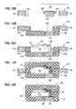
- FIG. 1 is a bottom plan view of a memory card fabricated through the use of a tape supported leadframe in accordance with the present invention
- FIG. 2 is a top plan view of the leadframe of the memory card shown in FIG. 1 prior to the application of the tape thereto;
- FIGS. 3A and 3B are top plan views of the leadframe of the memory card illustrating an exemplary sequence of steps which may be used to facilitate the application of tape thereto and the singulation of the tie bars thereof in accordance with a first embodiment of the present invention
- FIG. 4 is a partial cross-sectional view of a memory card formed through the implementation of the fabrication steps shown in FIGS. 3A and 3B ;
- FIGS. 5A and 5B are bottom plan views of the leadframe of the memory card illustrating an exemplary sequence of steps which may be used to facilitate the application of the tape thereto and the singulation of the tie bars thereof in accordance with a second embodiment of the present invention
- FIG. 6 is a partial cross-sectional view of a memory card formed through the implementation of the fabrication steps shown in FIGS. 5A and 5B ;
- FIGS. 7A and 7B are top plan views of the leadframe of the memory card illustrating an exemplary sequence of steps which may be used to facilitate the application of tape thereto and the singulation of the tie bars thereof in accordance with a third embodiment of the present invention
- FIG. 8 is a partial cross-sectional view of a memory card formed through the implementation of the fabrication steps shown in FIGS. 7A and 7B ;
- FIGS. 9A and 9B are top plan views of the leadframe of the memory card illustrating an exemplary sequence of steps which may be used to facilitate the application of tape thereto and the singulation of the tie bars thereof in accordance with a fourth embodiment of the present invention
- FIG. 10 is a partial cross-sectional view of a memory card formed through the implementation of the fabrication steps shown in FIGS. 9A and 9B ;
- FIG. 11 is a partial cross-sectional view of the memory cards shown in FIGS. 6 , and 10 subsequent to the removal of the tape from the ESC pads thereof;
- FIGS. 12A–12E illustrate an exemplary sequence of steps which may be used to facilitate fabrication of a memory card in accordance with a fifth embodiment of the present invention
- FIG. 13 is a top plan view of the leadframe of the memory card having tape applied thereto in accordance with the fifth embodiment, the side elevational view of which is shown in FIG. 12A ;
- FIG. 14 is a partial cross-sectional view of a memory card formed in accordance with a sixth embodiment of the present invention.
- FIG. 1 depicts a memory card 10 which includes a leadframe 12 best shown in FIG. 2 .
- the memory card 10 has a form factor particularly suited for use in a multi-media card memory application.
- the memory card 10 may have alternative memory card formats, including those of secure digital cards (SDC), compact flash (CF), smart media, memory stick, and other small form factor memory cards.
- the leadframe 12 of the memory card 10 comprises an outer frame or dambar 14 which is eventually removed from the leadframe 12 as described below, and thus does not constitute part of the completed memory card 10 .
- Dambar 14 has a generally rectangular configuration defining an opposed pair of longitudinal sides or segments 16 and an opposed pair of lateral sides or segments 18 .
- the leadframe 12 includes a die attach area or die pad 20 which is disposed within the interior of the dambar 14 .
- Die pad 20 defines opposed, generally planar top and bottom surfaces.
- Integrally connected to and extending from one lateral side 18 of the dambar 14 is a plurality of contacts 22 of the leadframe 12 . Each of the contacts 22 also defines opposed, generally planar top and bottom surfaces.
- a conductive trace 24 Integrally connected to and extending from each of the contacts 22 is a conductive trace 24 .
- the traces 24 terminate in close proximity to the die pad 20 .
- Tie bars 26 are used to integrally connect the die pad 20 to the longitudinal sides 16 of the dambar 14 .
- one or more tie bars 27 are used to integrally connect the contacts 22 to one lateral side 18 of the dambar 14 .
- two tie bars 27 are integrally connected to and extend between each contact 22 and the corresponding lateral side 18 , though one or more than two tie bars 27 may be used to facilitate such connection.
- a pair of semiconductor dies 30 is shown as being attached and electrically connected to a common interposer or laminate substrate 31 , which is in turn attached to the top surface of the die pad 20 .
- the semiconductor dies 30 and/or the substrate 31 are electrically connected to the leadframe 12 , and more particularly to one or more traces 24 , the die pad 20 , and/or each other through the use of conductive wires 32 .
- the conductive wires 32 effectively place the semiconductor dies 30 into electrical communication with the leadframe 12 and, more particularly, to one or more of the contacts 22 thereof.
- the leadframe 12 is preferably fabricated from a conductive metal material (e.g., copper) through either a chemical etching or mechanical stamping process.
- a conductive metal material e.g., copper
- the leadframe 12 may be formed to include any number of contacts 22 depending on the desired application for the memory card 10 . As shown in FIG. 1 , the memory card 10 includes seven contacts 22 which is the typical number included for a multi-media card application.
- the leadframe 12 may further be alternatively configured to define more than one die pad, with the die pad(s) accommodating one or more semiconductor dies alone or in combination with other devices such as passive devices. Additionally, the two semiconductor dies 30 shown in FIG. 2 may be attached directly to the die pad 20 as opposed to the intervening substrate 31 .
- the two semiconductor dies 30 shown in FIG. 2 may be substituted with one or more than two semiconductor dies alone or in combination with one or more other devices. Still further, one or more than two semiconductor dies and/or one or more other devices can be attached to a single die pad, or to respective ones of multiple dies pads, such semiconductor die(s) and/or other device(s) being attached either directly to the die pad(s) or to one or more intervening substrates.
- the pattern of conductive traces 24 may also be varied depending upon the number and arrangement of die pads and the number of semiconductor dies and/or other passive devices included in the memory card 10 .
- the configuration of the leadframe 12 of the memory card 10 is variable, in that the number and arrangement of die pads, contacts, and conductive traces may be varied as needed to satisfy the requirements of a particular application.
- the number and arrangement of the semiconductor dies 30 shown in FIG. 2 is also exemplary only in that such number and arrangement may also be varied based on specific application requirements.
- the memory card 10 is fabricated by initially forming the leadframe 12 to have the above-described structural attributes. Thereafter, an elongate strip or layer of tape 44 is applied to the top surface of the leadframe 12 . More particularly, as shown in FIG. 3A , the tape 44 is applied to the top surface of the leadframe 12 such that the top surfaces of the contacts 22 and the top surfaces of the tie bars 27 are completely covered by the tape 44 , with portions of the top surfaces of the traces 24 and a portion of the top surface of the lateral side 18 to which the tie bars 27 are connected being partially covered by the tape 44 . As further seen in FIG. 3A , the tape 44 also extends to and covers portions of the top surfaces of the longitudinal sides 16 of the dambar 14 .
- a singulation (e.g., a punching) operation is completed which effectively facilitates the removal of the tie bars 27 from the leadframe 12 . More particularly, the tie bars 27 are punched-out through the tape 44 , thus effectively separating the contacts 22 from the dambar 14 , and electrically isolating the contacts 22 from each other. Subsequent to the completion of the punching operation, the semiconductor die(s) 30 and/or other devices are secured to the top surface of the die pad 20 and electrically connected thereto and/or to the traces 24 through the use of the conductive wires 32 . Those of ordinary skill in the art will recognize that the application of the tape 44 to the leadframe 12 and removal of the tie bars 27 could occur subsequent to the attachment and electrical connection of the semiconductor die(s) 30 and/or other devices to the leadframe 12 .
- an encapsulant material is applied to the leadframe 12 , the semiconductor die(s) 30 , and conductive wires 32 .
- the encapsulant is further applied to the portion of the tape 44 remaining subsequent to the removal of the tie bars 27 by the punching operation.
- the encapsulant material is preferably a plastic (e.g., thermoset, thermoplastic) which, upon hardening, forms a body 34 of the memory card 10 .
- the body 34 is formed to provide a prescribed form factor for the memory card 10 .
- the body 34 defines a generally planar top surface 35 , and an opposed, generally planar bottom surface 36 .
- the body 34 defines an opposed pair of longitudinal sides 38 , an opposed pair of lateral sides 40 , and a fifth sloped side 42 which extends angularly between one of the lateral sides 40 and one of the longitudinal sides 38 .
- the bottom surfaces of the contacts 22 of the leadframe 12 are exposed in and generally flush with the bottom surface 36 of the body 34 .
- the tape 44 is embedded within the body 34 in the manner best shown in FIG. 4 .
- one edge of the tape 44 extends to and is thus exposed in the leading edge or side 40 of the body 34 , i.e., the side 40 adjacent to and extending along the contacts 22 .
- a layer of epoxy may be applied to the leadframe 12 in a manner covering those portions thereof described above as being covered by the tape 44 . The hardening of the epoxy creates a layer which provides the same functional attributes as the tape 44 .
- the fabrication of the memory card 10 through the application of the tape 44 or epoxy layer to the leadframe 12 provides significant advantages over currently known fabrication techniques.
- the body 34 would be formed on the leadframe 12 such that the dambar 14 and portions of the tie bars 26 , 27 remain exposed (i.e., are not covered by the body 34 ).
- the exposure of the dambar 14 and portions of the tie bars 26 , 27 allows for the removal of the same from the completely formed body 34 .
- the leaframe 12 would be cut or singulated in a manner facilitating the removal of the dambar 14 as is needed to electrically isolate the traces 24 and hence the contacts 22 from each other.
- the severing of the tie bars 27 result in the severed distal ends thereof still being exposed in the leading edge of the body 34 .
- Such exposure gives rise to potential occurrences of shorting against the metal features of the host socket.
- the memory card 10 is fabricated by essentially the same process described above in relation to FIGS. 3A , 3 B and 4 , except that the tape 44 is applied to the bottom surface of the leadframe 12 , rather than to the top surface thereof as described in relation to the first embodiment. More particularly, as shown in FIG. 5A , the tape 44 is applied to the bottom surface of the leadframe 12 such that the bottom surfaces of the contacts 22 and the bottom surfaces of the tie bars 27 are completely covered by the tape 44 , with portions of the bottom surfaces of the traces 24 and a portion of the bottom surface of the lateral side 18 to which the tie bars 27 are connected being partially covered by the tape 44 .
- the tape 44 also extends to and covers portions of the bottom surfaces of the longitudinal sides 16 of the dambar 14 .
- the traces 24 of the leaframe 12 are optionally “upset” (i.e., perpendicularly recessed or offset relative to the bottom surfaces of the contacts 22 )
- the tape 44 will not cover the bottom surfaces of the traces 24 , but rather will be spaced therefrom.
- the above-described punching operation is completed to effectively facilitate the removal of the tie bars 27 from the leadframe 12 in the manner shown in FIG. 5B .
- the body 34 of the memory card 10 is formed in the above-described manner. As seen in FIG.
- the tape 44 is not embedded within the body 34 , but rather simply extends over the bottom surfaces of the contacts 22 and a portion of the bottom surface 36 of the body 34 .
- the tape 44 may be completely removed, thus causing the memory card 10 to have the cross-sectional configuration shown in FIG. 11 , the tape 44 not constituting part of the complete memory card 10 .
- the memory card 10 is fabricated by essentially the same process described above in relation to FIGS. 3A , 3 B and 4 , except that the tape 44 is applied to both the top and bottom surfaces of the leadframe 12 , rather than only to the top surface thereof as described in relation to the first embodiment, or only to the bottom surface thereof as described in relation to the second embodiment. More particularly, as shown in FIG. 7A , the tape 44 is applied to both the top and bottom surfaces of the leadframe 12 such that the top and bottom surfaces of the contacts 22 and the top and bottom surfaces of the tie bars 27 are completely covered by respective layers of the tape 44 .
- Portions of the top and bottom surfaces of the traces 24 and portions of the top and bottom surfaces of the lateral side 18 to which the tie bars 27 are connected are partially covered by respective layers of the tape 44 .
- the layers of tape 44 also extend to and cover portions of the top and bottom surfaces of the longitudinal sides 16 of the dambar 14 .
- the above-described punching operation is completed to effectively facilitate the removal of the tie bars 27 from the leadframe 12 in the manner shown in FIG. 7B .
- the punching operation is completed in a manner wherein a single, elongate slot is formed through the layers of tape 44 as is shown in FIG. 7B .
- the body 34 of the memory card 10 in the third embodiment is formed in the same manner described above in relation to the first and second embodiments.
- the layer of tape 44 applied to the top surface of the leadframe 12 is embedded within the body 34 , with one edge thereof extending to and thus being exposed in the leading edge or side 40 of the body 34 .
- the layer of tape 44 attached to the bottom surface of the leadframe 12 is not embedded within the body 34 of the fully formed memory card 10 , but rather simply extends over the bottom surfaces of the contacts 22 and a portion of the bottom surface 36 of the body 34 . Thus, subsequent to the formation of the body 34 , this bottom layer of tape 44 may be completely removed, thus causing the memory card 10 to have the cross-sectional configuration shown in FIG. 4 .
- the memory card 10 is fabricated by essentially the same process described above in relation to FIGS. 5A , 5 B and 6 , except that the width of the layer of tape 44 applied to the bottom surface of the leadframe 12 in the fourth embodiment substantially exceeds that of the tape 44 applied to the bottom surface of the leadframe 12 in the second embodiment. More particularly, as shown in FIG. 9A , the tape 44 is applied to the bottom surface of the leadframe 12 such that the bottom surfaces of the contacts 22 , the bottom surfaces of the traces 24 , the bottom surfaces of the tie bars 26 , 27 , and the bottom surface of the die pad 20 are completely covered by the tape 44 .
- the tape 44 also extends to and covers at least portions of the bottom surfaces of the longitudinal and lateral sides 16 , 18 of the dambar 14 .
- the tape 44 may be spaced from the bottom surfaces of the traces 24 and the tie bars 26 , 27 in the event the leadframe 12 is optionally subjected to a half-etching process wherever the bottom surfaces of the traces 24 and tie bars 26 , 27 are perpendicularly recessed relative to the bottom surfaces of the die pad 20 and contacts 22 .
- the above-described punching operation is completed to effectively facilitate the removal of the tie bars 27 from the leadframe 12 in the manner shown in FIG. 9B .
- the body 34 of the memory card 10 is formed in the above-described manner. As seen in FIG.
- the tape 44 is not embedded in the body 34 , but rather simply extends over the entire bottom surface 36 of the body 34 , including the bottom surfaces of the contacts 22 .
- the tape 44 may be completely removed, thus causing the memory card 10 to have the cross-sectional configuration shown in FIG. 11 wherein the tape 44 does not constitute part of the complete memory card 10 .
- the layer(s) of tape 44 may be substituted with epoxy in the manner described in relation to the first embodiment.
- the punching operation may be completed so as to facilitate the formation of the series of openings as shown in FIGS. 3B , 5 B, and 9 B, or the single elongate slot as shown in FIG. 7B .
- the openings or slot created as a result of the punching operation must be sized and configured as necessary to ensure the complete removal of all of the tie bars 27 extending between the contacts 22 and the dambar 14 .
- the memory card 46 comprises a leadframe 48 having an outer frame or dambar 50 .
- Dambar 50 has a generally quadrangular configuration defining an opposed pair of longitudinal sides or segments 52 and an opposed pair of lateral sides or segments 54 .
- Disposed within the interior of the dambar 50 is a plurality of contacts 56 of the leadframe 48 .
- the contacts 56 are linearly aligned and extend in spaced, generally parallel relation to one of the lateral sides 54 of the dambar 50 .
- each contact 56 includes a pair of locking tabs 58 extending from respective ones of the opposed ends thereof. As seen in FIG. 12A , the thickness of each contact 56 substantially exceeds the thickness of each of the locking tabs 58 of the pair protruding therefrom. Additionally, formed on and extending inwardly from the lateral side 54 of the dambar 50 opposite that along which the contacts 56 extend is a pair of locking tabs 60 . Like the locking tabs 58 , the locking tabs 60 are formed such that the thicknesses thereof are substantially less than that of the dambar 50 , as is also seen in FIG. 12A . The use of the locking tabs 58 , 60 will be described in more detail below.
- the leadframe 48 used to fabricate the memory card 46 does not include a die pad. Nor are tie bars used to connect the contacts 56 of the leadframe 48 to the adjacent lateral side 54 of the dambar 50 . Rather, to facilitate the fabrication of the memory card 46 , the contacts 56 are maintained in prescribed orientations relative to each other and to the dambar 50 via an elongate layer or strip of tape 62 .
- the tape 62 is applied to the top surface of the leadframe 48 such that the top surfaces of the contacts 56 and portions of the longitudinal sides 52 of the dambar 50 are covered by the tape 62 .
- a first molding process is completed to facilitate the fabrication of a lower body section 64 of the memory card 46 ( FIG. 12B ).
- downward pressure is applied to the tape 62 and hence to the contacts 56 in a manner which causes the contacts 56 to be vertically downset or recessed relative to the dambar 50 in the manner shown in FIG. 12B .
- the tape 62 has sufficient pliability so as to allow for such downsetting of the contacts 56 , despite the opposed ends portions of the tape 62 being maintained in engagement to the longitudinal sides 52 of the dambar 50 .
- the formation of the lower body section 64 occurrs subsequent to such downsetting of the contacts 56 .
- the contacts 56 are effectively mechanically interlocked to the lower body section 64 as a result of the flow of the encapsulant material which ultimately hardens into the lower body section 64 about the locking tabs 58 of each contact 56 .
- the encapsulant material which ultimately hardens into the lower body section 64 also flows about the locking tabs 60 protruding inwardly from one lateral side 54 of the dambar 50 .
- the lower body section 64 is formed to have a radiused edge which extends around the entire perimeter of the generally planar bottom surface thereof. The generally planar bottom surfaces of the contacts 56 are also exposed in and substantially flush with the bottom surface of the lower body section 64 .
- an electronic component 66 is mounted within a cavity defined by the lower body section 64 , and electrically connected to the top surface of at least one of the contacts 56 by a conductive wire 68 ( FIG. 12C ).
- the electronic component comprises a laminate substrate 70 having a semiconductor die 72 which is mounted to the top surface thereof and electrically connected thereto, the substrate 70 in turn being electrically connected to one or more of the contacts 56 by one or more wires 68 .
- the tape 62 will not be removed from the top surfaces of the contacts 56 , it will be recognized that portions of the tape will need to be removed as necessary to allow for the advancement of the wire(s) 68 to the top surface(s) of the contact(s) 56 . However, it is further contemplated that the tape 62 may be completely removed from the top surfaces of the contacts 56 subsequent to the formation of the lower body section 64 . Those of ordinary skill in the art will further appreciate that the electronic component 66 shown and described in relation to FIG.
- 12C is exemplary only, in that one or more semiconductor dies and/or one or more other devices, mounted or not mounted to a laminate substrate, may be placed into the cavity of the lower body section 64 and electrically connected to the contact(s) 56 with or without the use of the conductive wire(s) 68 .
- a second molding operation is completed to facilitate the formation of an upper body section 74 upon the lower body section 64 ( FIG. 12D ).
- the lower body section 74 fills the open areas of the cavity defined by the lower body section 64 , and completely covers or encapsulates the electronic component 66 and the wire(s) 68 (if any) used to electrically connect the electronic component 66 to the contacts 56 .
- the upper body section 74 is preferably molded such that a radiused edge extends about the entire perimeter of the generally planar top surface of the upper body section 74 .
- the fully formed memory card 46 has a body which is collectively defined by the lower and upper body sections 64 , 74 described above. Due to the complete absence of any tie bars in the leadframe 48 , the leading edge or side 76 of the body of the memory card 46 does not have any tie bar ends exposed therein.
- FIG. 14 there is shown a partial cross-section of a memory card 78 formed in accordance with a sixth embodiment of the present invention.
- the memory card 78 includes the above-described leadframe 12 .
- no layer of tape is applied to either the top or bottom surfaces of the leadframe 12 .
- the body 34 is formed on the leadframe 12 in the above-described manner.
- the tie bars 27 are not punched or otherwise removed from the leadframe 12 , upon the formation of the body 34 and singulation of the dambar 14 from the remainder of the leadframe 12 , the severed distal ends of the tie bars 27 will be exposed in the leading edge or side 40 of the body 34 , i.e., the side 40 adjacent to and extending along the contacts 22 .
- a milling or etching process is conducted upon the lower peripheral edge or corner of the leading side 40 of the body 34 , this milling or etching procedure imparting a contoured profile to a portion of such leading side 40 in the manner shown in FIG. 14 .
- the distal ends of the tie bars 27 are exposed only in the contoured portion of the leading side 40 , and thus are recessed relative that portion of the side 40 which is unaffected by the milling or etching procedure.
- the contoured portion of the leading side 40 of the body 34 creates a safety margin S as shown in FIG. 14 wherein the exposed ends of the tie bars 27 are substantially prevented from making contact with the metal features of the host socket.
Abstract
Description
Claims (15)
Priority Applications (2)
| Application Number | Priority Date | Filing Date | Title |
|---|---|---|---|
| US10/828,616 US7074654B1 (en) | 2004-04-21 | 2004-04-21 | Tape supported memory card leadframe structure |
| US11/425,502 US7556986B1 (en) | 2004-04-21 | 2006-06-21 | Tape supported memory card leadframe structure |
Applications Claiming Priority (1)
| Application Number | Priority Date | Filing Date | Title |
|---|---|---|---|
| US10/828,616 US7074654B1 (en) | 2004-04-21 | 2004-04-21 | Tape supported memory card leadframe structure |
Related Child Applications (1)
| Application Number | Title | Priority Date | Filing Date |
|---|---|---|---|
| US11/425,502 Continuation-In-Part US7556986B1 (en) | 2004-04-21 | 2006-06-21 | Tape supported memory card leadframe structure |
Publications (1)
| Publication Number | Publication Date |
|---|---|
| US7074654B1 true US7074654B1 (en) | 2006-07-11 |
Family
ID=36644046
Family Applications (1)
| Application Number | Title | Priority Date | Filing Date |
|---|---|---|---|
| US10/828,616 Active 2024-10-10 US7074654B1 (en) | 2004-04-21 | 2004-04-21 | Tape supported memory card leadframe structure |
Country Status (1)
| Country | Link |
|---|---|
| US (1) | US7074654B1 (en) |
Cited By (2)
| Publication number | Priority date | Publication date | Assignee | Title |
|---|---|---|---|---|
| US20080185694A1 (en) * | 1999-08-04 | 2008-08-07 | Super Talent Electronics, Inc. | Processes of Manufacturing Portable Electronic Storage Devices Utilizing Lead Frame Connectors |
| US20080283983A1 (en) * | 2007-03-26 | 2008-11-20 | Mitsubishi Electric Corporation | Semiconductor device and manufacturing method thereof |
Citations (26)
| Publication number | Priority date | Publication date | Assignee | Title |
|---|---|---|---|---|
| US3668299A (en) | 1971-04-29 | 1972-06-06 | Beckman Instruments Inc | Electrical circuit module and method of assembly |
| US4532419A (en) | 1982-09-09 | 1985-07-30 | Sony Corporation | Memory card having static electricity protection |
| US4905124A (en) | 1987-03-31 | 1990-02-27 | Mitsubishi Denki Kabushiki Kaisha | IC card |
| US4974120A (en) | 1989-01-12 | 1990-11-27 | Mitsubishi Denki Kabushiki Kaisha | IC card |
| JPH03112688A (en) | 1989-09-27 | 1991-05-14 | Asahi Chem Ind Co Ltd | Ic card |
| US5172214A (en) | 1991-02-06 | 1992-12-15 | Motorola, Inc. | Leadless semiconductor device and method for making the same |
| US5360992A (en) | 1991-12-20 | 1994-11-01 | Micron Technology, Inc. | Two piece assembly for the selection of pinouts and bond options on a semiconductor device |
| JPH0717175A (en) | 1993-06-22 | 1995-01-20 | Seiko Epson Corp | Memory card |
| JPH08190615A (en) | 1995-01-09 | 1996-07-23 | Seiko Epson Corp | Memory card |
| US5574309A (en) | 1991-11-25 | 1996-11-12 | Gemplus Card International | Integrated circuit card comprising means for the protection of the integrated circuit |
| US5742479A (en) | 1994-03-09 | 1998-04-21 | Seiko Epson Corporation | Card-type electronic device with plastic frame sandwiched between printed circuit board and metal panel |
| US5753532A (en) | 1995-08-30 | 1998-05-19 | Samsung Electronics Co., Ltd. | Method of manufacturing semiconductor chip package |
| US5822190A (en) | 1996-06-11 | 1998-10-13 | Kabushiki Kaisha Toshiba | Card type memory device and a method for manufacturing the same |
| JPH10334205A (en) | 1997-05-30 | 1998-12-18 | Toshiba Corp | Ic card and memory package |
| US5977613A (en) | 1996-03-07 | 1999-11-02 | Matsushita Electronics Corporation | Electronic component, method for making the same, and lead frame and mold assembly for use therein |
| US6040622A (en) | 1998-06-11 | 2000-03-21 | Sandisk Corporation | Semiconductor package using terminals formed on a conductive layer of a circuit board |
| US6143981A (en) | 1998-06-24 | 2000-11-07 | Amkor Technology, Inc. | Plastic integrated circuit package and method and leadframe for making the package |
| US6249042B1 (en) * | 1998-06-19 | 2001-06-19 | Sumitomo Electric Industries Ltd | Member for lead |
| USD445096S1 (en) | 1998-04-01 | 2001-07-17 | Sandisk Corporation | Removable memory card for use with portable electronic devices |
| USD446525S1 (en) | 1999-08-24 | 2001-08-14 | Kabushiki Kaisha Toshiba | IC memory card |
| US6384472B1 (en) | 2000-03-24 | 2002-05-07 | Siliconware Precision Industries Co., Ltd | Leadless image sensor package structure and method for making the same |
| US20020140068A1 (en) | 2001-03-28 | 2002-10-03 | Ming-Hsun Lee | Leadframe-based semiconductor package for multi-media card |
| US6476469B2 (en) | 2000-11-23 | 2002-11-05 | Siliconware Precision Industries Co., Ltd. | Quad flat non-leaded package structure for housing CMOS sensor |
| US6545332B2 (en) | 2001-01-17 | 2003-04-08 | Siliconware Precision Industries Co., Ltd. | Image sensor of a quad flat package |
| US6624005B1 (en) | 2000-09-06 | 2003-09-23 | Amkor Technology, Inc. | Semiconductor memory cards and method of making same |
| US20040104457A1 (en) * | 2002-11-27 | 2004-06-03 | United Test And Assembly Test Center Ltd. | High density chip scale leadframe package and method of manufacturing the package |
-
2004
- 2004-04-21 US US10/828,616 patent/US7074654B1/en active Active
Patent Citations (28)
| Publication number | Priority date | Publication date | Assignee | Title |
|---|---|---|---|---|
| US3668299A (en) | 1971-04-29 | 1972-06-06 | Beckman Instruments Inc | Electrical circuit module and method of assembly |
| US4532419A (en) | 1982-09-09 | 1985-07-30 | Sony Corporation | Memory card having static electricity protection |
| US4905124A (en) | 1987-03-31 | 1990-02-27 | Mitsubishi Denki Kabushiki Kaisha | IC card |
| US4974120A (en) | 1989-01-12 | 1990-11-27 | Mitsubishi Denki Kabushiki Kaisha | IC card |
| JPH03112688A (en) | 1989-09-27 | 1991-05-14 | Asahi Chem Ind Co Ltd | Ic card |
| US5172214A (en) | 1991-02-06 | 1992-12-15 | Motorola, Inc. | Leadless semiconductor device and method for making the same |
| US5574309A (en) | 1991-11-25 | 1996-11-12 | Gemplus Card International | Integrated circuit card comprising means for the protection of the integrated circuit |
| US5360992A (en) | 1991-12-20 | 1994-11-01 | Micron Technology, Inc. | Two piece assembly for the selection of pinouts and bond options on a semiconductor device |
| JPH0717175A (en) | 1993-06-22 | 1995-01-20 | Seiko Epson Corp | Memory card |
| US5742479A (en) | 1994-03-09 | 1998-04-21 | Seiko Epson Corporation | Card-type electronic device with plastic frame sandwiched between printed circuit board and metal panel |
| US5784259A (en) | 1994-03-09 | 1998-07-21 | Seiko Epson Corporation | Card-type electronic device with plastic frame sandwiched between printed circuit boarding metal panel |
| JPH08190615A (en) | 1995-01-09 | 1996-07-23 | Seiko Epson Corp | Memory card |
| US5753532A (en) | 1995-08-30 | 1998-05-19 | Samsung Electronics Co., Ltd. | Method of manufacturing semiconductor chip package |
| US5977613A (en) | 1996-03-07 | 1999-11-02 | Matsushita Electronics Corporation | Electronic component, method for making the same, and lead frame and mold assembly for use therein |
| US5822190A (en) | 1996-06-11 | 1998-10-13 | Kabushiki Kaisha Toshiba | Card type memory device and a method for manufacturing the same |
| JPH10334205A (en) | 1997-05-30 | 1998-12-18 | Toshiba Corp | Ic card and memory package |
| USD445096S1 (en) | 1998-04-01 | 2001-07-17 | Sandisk Corporation | Removable memory card for use with portable electronic devices |
| US6040622A (en) | 1998-06-11 | 2000-03-21 | Sandisk Corporation | Semiconductor package using terminals formed on a conductive layer of a circuit board |
| US6249042B1 (en) * | 1998-06-19 | 2001-06-19 | Sumitomo Electric Industries Ltd | Member for lead |
| US6143981A (en) | 1998-06-24 | 2000-11-07 | Amkor Technology, Inc. | Plastic integrated circuit package and method and leadframe for making the package |
| USD446525S1 (en) | 1999-08-24 | 2001-08-14 | Kabushiki Kaisha Toshiba | IC memory card |
| US6384472B1 (en) | 2000-03-24 | 2002-05-07 | Siliconware Precision Industries Co., Ltd | Leadless image sensor package structure and method for making the same |
| US6624005B1 (en) | 2000-09-06 | 2003-09-23 | Amkor Technology, Inc. | Semiconductor memory cards and method of making same |
| US6476469B2 (en) | 2000-11-23 | 2002-11-05 | Siliconware Precision Industries Co., Ltd. | Quad flat non-leaded package structure for housing CMOS sensor |
| US6545332B2 (en) | 2001-01-17 | 2003-04-08 | Siliconware Precision Industries Co., Ltd. | Image sensor of a quad flat package |
| US20020140068A1 (en) | 2001-03-28 | 2002-10-03 | Ming-Hsun Lee | Leadframe-based semiconductor package for multi-media card |
| US6603196B2 (en) | 2001-03-28 | 2003-08-05 | Siliconware Precision Industries Co., Ltd. | Leadframe-based semiconductor package for multi-media card |
| US20040104457A1 (en) * | 2002-11-27 | 2004-06-03 | United Test And Assembly Test Center Ltd. | High density chip scale leadframe package and method of manufacturing the package |
Cited By (5)
| Publication number | Priority date | Publication date | Assignee | Title |
|---|---|---|---|---|
| US20080185694A1 (en) * | 1999-08-04 | 2008-08-07 | Super Talent Electronics, Inc. | Processes of Manufacturing Portable Electronic Storage Devices Utilizing Lead Frame Connectors |
| US20080283983A1 (en) * | 2007-03-26 | 2008-11-20 | Mitsubishi Electric Corporation | Semiconductor device and manufacturing method thereof |
| US7892893B2 (en) * | 2007-03-26 | 2011-02-22 | Mitsubishi Electric Corporation | Semiconductor device and manufacturing method thereof |
| US20110108964A1 (en) * | 2007-03-26 | 2011-05-12 | Mitsubishi Electric Corporation | Semiconductor device and manufacturing method thereof |
| US8093692B2 (en) | 2007-03-26 | 2012-01-10 | Mitsubishi Electric Corporation | Semiconductor device packaging including a power semiconductor element |
Similar Documents
| Publication | Publication Date | Title |
|---|---|---|
| US7112875B1 (en) | Secure digital memory card using land grid array structure | |
| US7011251B1 (en) | Die down multi-media card and method of making same | |
| US7279781B2 (en) | Two-stage transfer molding device to encapsulate MMC module | |
| US6462273B1 (en) | Semiconductor card and method of fabrication | |
| US7795715B2 (en) | Leadframe based flash memory cards | |
| TWI249712B (en) | Memory card and its manufacturing method | |
| US7960818B1 (en) | Conformal shield on punch QFN semiconductor package | |
| US6965159B1 (en) | Reinforced lead-frame assembly for interconnecting circuits within a circuit module | |
| US7220915B1 (en) | Memory card and its manufacturing method | |
| US7633763B1 (en) | Double mold memory card and its manufacturing method | |
| US7719845B1 (en) | Chamfered memory card module and method of making same | |
| US6911718B1 (en) | Double downset double dambar suspended leadframe | |
| US7095103B1 (en) | Leadframe based memory card | |
| JP3137323B2 (en) | Semiconductor device and manufacturing method thereof | |
| US7193305B1 (en) | Memory card ESC substrate insert | |
| US7074654B1 (en) | Tape supported memory card leadframe structure | |
| US7556986B1 (en) | Tape supported memory card leadframe structure | |
| US6897550B1 (en) | Fully-molded leadframe stand-off feature | |
| US6717822B1 (en) | Lead-frame method and circuit module assembly including edge stiffener | |
| US6921967B2 (en) | Reinforced die pad support structure | |
| US8927343B2 (en) | Package process | |
| US7201327B1 (en) | Memory card and its manufacturing method | |
| US20080003722A1 (en) | Transfer mold solution for molded multi-media card | |
| US10763203B1 (en) | Conductive trace design for smart card | |
| US7485952B1 (en) | Drop resistant bumpers for fully molded memory cards |
Legal Events
| Date | Code | Title | Description |
|---|---|---|---|
| AS | Assignment |
Owner name: AMKOR TECHNOLOGY, INC., ARIZONA Free format text: ASSIGNMENT OF ASSIGNORS INTEREST;ASSIGNORS:D'ESTRIES, MAXIMILIEN;MIKS, JEFFREY A.;ZWENGER, CURTIS M.;AND OTHERS;REEL/FRAME:015228/0031 Effective date: 20040413 |
|
| STCF | Information on status: patent grant |
Free format text: PATENTED CASE |
|
| AS | Assignment |
Owner name: BANK OF AMERICA, N.A., TEXAS Free format text: PATENT SECURITY AGREEMENT;ASSIGNOR:AMKOR TECHNOLOGY, INC.;REEL/FRAME:022764/0864 Effective date: 20090416 Owner name: BANK OF AMERICA, N.A.,TEXAS Free format text: PATENT SECURITY AGREEMENT;ASSIGNOR:AMKOR TECHNOLOGY, INC.;REEL/FRAME:022764/0864 Effective date: 20090416 |
|
| FPAY | Fee payment |
Year of fee payment: 4 |
|
| FPAY | Fee payment |
Year of fee payment: 8 |
|
| MAFP | Maintenance fee payment |
Free format text: PAYMENT OF MAINTENANCE FEE, 12TH YEAR, LARGE ENTITY (ORIGINAL EVENT CODE: M1553) Year of fee payment: 12 |
|
| AS | Assignment |
Owner name: BANK OF AMERICA, N.A., AS AGENT, CALIFORNIA Free format text: SECURITY INTEREST;ASSIGNOR:AMKOR TECHNOLOGY, INC.;REEL/FRAME:046683/0139 Effective date: 20180713 |
|
| AS | Assignment |
Owner name: AMKOR TECHNOLOGY SINGAPORE HOLDING PTE.LTD., SINGAPORE Free format text: ASSIGNMENT OF ASSIGNORS INTEREST;ASSIGNOR:AMKOR TECHNOLOGY, INC.;REEL/FRAME:054067/0135 Effective date: 20191119 |