US7064088B2 - Method for forming low-k hard film - Google Patents
Method for forming low-k hard film Download PDFInfo
- Publication number
- US7064088B2 US7064088B2 US10/412,363 US41236303A US7064088B2 US 7064088 B2 US7064088 B2 US 7064088B2 US 41236303 A US41236303 A US 41236303A US 7064088 B2 US7064088 B2 US 7064088B2
- Authority
- US
- United States
- Prior art keywords
- reaction
- gas
- silicon
- containing hydrocarbon
- compound
- Prior art date
- Legal status (The legal status is an assumption and is not a legal conclusion. Google has not performed a legal analysis and makes no representation as to the accuracy of the status listed.)
- Expired - Lifetime, expires
Links
- 0 [1*][Si]([2*])(OC)OC Chemical compound [1*][Si]([2*])(OC)OC 0.000 description 7
- BVTLTBONLZSBJC-UHFFFAOYSA-N C=C[Si]1(C)O[Si](C)(C=C)O[Si](C)(C=C)O1 Chemical compound C=C[Si]1(C)O[Si](C)(C=C)O[Si](C)(C=C)O1 BVTLTBONLZSBJC-UHFFFAOYSA-N 0.000 description 1
- ZNOCGWVLWPVKAO-UHFFFAOYSA-N CO[Si](OC)(OC)C1=CC=CC=C1 Chemical compound CO[Si](OC)(OC)C1=CC=CC=C1 ZNOCGWVLWPVKAO-UHFFFAOYSA-N 0.000 description 1
- VUASWCWRQJUEPH-UHFFFAOYSA-N CO[Si]1(C)O[Si](C)(OC)O[Si](C)(OC)O1 Chemical compound CO[Si]1(C)O[Si](C)(OC)O[Si](C)(OC)O1 VUASWCWRQJUEPH-UHFFFAOYSA-N 0.000 description 1
- HTDJPCNNEPUOOQ-UHFFFAOYSA-N C[Si]1(C)O[Si](C)(C)O[Si](C)(C)O1 Chemical compound C[Si]1(C)O[Si](C)(C)O[Si](C)(C)O1 HTDJPCNNEPUOOQ-UHFFFAOYSA-N 0.000 description 1
- HMMGMWAXVFQUOA-UHFFFAOYSA-N C[Si]1(C)O[Si](C)(C)O[Si](C)(C)O[Si](C)(C)O1 Chemical compound C[Si]1(C)O[Si](C)(C)O[Si](C)(C)O[Si](C)(C)O1 HMMGMWAXVFQUOA-UHFFFAOYSA-N 0.000 description 1
Images


Classifications
-
- B—PERFORMING OPERATIONS; TRANSPORTING
- B05—SPRAYING OR ATOMISING IN GENERAL; APPLYING FLUENT MATERIALS TO SURFACES, IN GENERAL
- B05D—PROCESSES FOR APPLYING FLUENT MATERIALS TO SURFACES, IN GENERAL
- B05D1/00—Processes for applying liquids or other fluent materials
- B05D1/62—Plasma-deposition of organic layers
-
- C—CHEMISTRY; METALLURGY
- C09—DYES; PAINTS; POLISHES; NATURAL RESINS; ADHESIVES; COMPOSITIONS NOT OTHERWISE PROVIDED FOR; APPLICATIONS OF MATERIALS NOT OTHERWISE PROVIDED FOR
- C09D—COATING COMPOSITIONS, e.g. PAINTS, VARNISHES OR LACQUERS; FILLING PASTES; CHEMICAL PAINT OR INK REMOVERS; INKS; CORRECTING FLUIDS; WOODSTAINS; PASTES OR SOLIDS FOR COLOURING OR PRINTING; USE OF MATERIALS THEREFOR
- C09D4/00—Coating compositions, e.g. paints, varnishes or lacquers, based on organic non-macromolecular compounds having at least one polymerisable carbon-to-carbon unsaturated bond ; Coating compositions, based on monomers of macromolecular compounds of groups C09D183/00 - C09D183/16
-
- C—CHEMISTRY; METALLURGY
- C23—COATING METALLIC MATERIAL; COATING MATERIAL WITH METALLIC MATERIAL; CHEMICAL SURFACE TREATMENT; DIFFUSION TREATMENT OF METALLIC MATERIAL; COATING BY VACUUM EVAPORATION, BY SPUTTERING, BY ION IMPLANTATION OR BY CHEMICAL VAPOUR DEPOSITION, IN GENERAL; INHIBITING CORROSION OF METALLIC MATERIAL OR INCRUSTATION IN GENERAL
- C23C—COATING METALLIC MATERIAL; COATING MATERIAL WITH METALLIC MATERIAL; SURFACE TREATMENT OF METALLIC MATERIAL BY DIFFUSION INTO THE SURFACE, BY CHEMICAL CONVERSION OR SUBSTITUTION; COATING BY VACUUM EVAPORATION, BY SPUTTERING, BY ION IMPLANTATION OR BY CHEMICAL VAPOUR DEPOSITION, IN GENERAL
- C23C16/00—Chemical coating by decomposition of gaseous compounds, without leaving reaction products of surface material in the coating, i.e. chemical vapour deposition [CVD] processes
- C23C16/22—Chemical coating by decomposition of gaseous compounds, without leaving reaction products of surface material in the coating, i.e. chemical vapour deposition [CVD] processes characterised by the deposition of inorganic material, other than metallic material
- C23C16/30—Deposition of compounds, mixtures or solid solutions, e.g. borides, carbides, nitrides
- C23C16/40—Oxides
- C23C16/401—Oxides containing silicon
-
- H—ELECTRICITY
- H01—ELECTRIC ELEMENTS
- H01L—SEMICONDUCTOR DEVICES NOT COVERED BY CLASS H10
- H01L21/00—Processes or apparatus adapted for the manufacture or treatment of semiconductor or solid state devices or of parts thereof
- H01L21/02—Manufacture or treatment of semiconductor devices or of parts thereof
- H01L21/02104—Forming layers
- H01L21/02107—Forming insulating materials on a substrate
- H01L21/02109—Forming insulating materials on a substrate characterised by the type of layer, e.g. type of material, porous/non-porous, pre-cursors, mixtures or laminates
- H01L21/02112—Forming insulating materials on a substrate characterised by the type of layer, e.g. type of material, porous/non-porous, pre-cursors, mixtures or laminates characterised by the material of the layer
- H01L21/02123—Forming insulating materials on a substrate characterised by the type of layer, e.g. type of material, porous/non-porous, pre-cursors, mixtures or laminates characterised by the material of the layer the material containing silicon
- H01L21/02126—Forming insulating materials on a substrate characterised by the type of layer, e.g. type of material, porous/non-porous, pre-cursors, mixtures or laminates characterised by the material of the layer the material containing silicon the material containing Si, O, and at least one of H, N, C, F, or other non-metal elements, e.g. SiOC, SiOC:H or SiONC
-
- H—ELECTRICITY
- H01—ELECTRIC ELEMENTS
- H01L—SEMICONDUCTOR DEVICES NOT COVERED BY CLASS H10
- H01L21/00—Processes or apparatus adapted for the manufacture or treatment of semiconductor or solid state devices or of parts thereof
- H01L21/02—Manufacture or treatment of semiconductor devices or of parts thereof
- H01L21/02104—Forming layers
- H01L21/02107—Forming insulating materials on a substrate
- H01L21/02109—Forming insulating materials on a substrate characterised by the type of layer, e.g. type of material, porous/non-porous, pre-cursors, mixtures or laminates
- H01L21/02205—Forming insulating materials on a substrate characterised by the type of layer, e.g. type of material, porous/non-porous, pre-cursors, mixtures or laminates the layer being characterised by the precursor material for deposition
- H01L21/02208—Forming insulating materials on a substrate characterised by the type of layer, e.g. type of material, porous/non-porous, pre-cursors, mixtures or laminates the layer being characterised by the precursor material for deposition the precursor containing a compound comprising Si
- H01L21/02214—Forming insulating materials on a substrate characterised by the type of layer, e.g. type of material, porous/non-porous, pre-cursors, mixtures or laminates the layer being characterised by the precursor material for deposition the precursor containing a compound comprising Si the compound comprising silicon and oxygen
- H01L21/02216—Forming insulating materials on a substrate characterised by the type of layer, e.g. type of material, porous/non-porous, pre-cursors, mixtures or laminates the layer being characterised by the precursor material for deposition the precursor containing a compound comprising Si the compound comprising silicon and oxygen the compound being a molecule comprising at least one silicon-oxygen bond and the compound having hydrogen or an organic group attached to the silicon or oxygen, e.g. a siloxane
-
- H—ELECTRICITY
- H01—ELECTRIC ELEMENTS
- H01L—SEMICONDUCTOR DEVICES NOT COVERED BY CLASS H10
- H01L21/00—Processes or apparatus adapted for the manufacture or treatment of semiconductor or solid state devices or of parts thereof
- H01L21/02—Manufacture or treatment of semiconductor devices or of parts thereof
- H01L21/02104—Forming layers
- H01L21/02107—Forming insulating materials on a substrate
- H01L21/02225—Forming insulating materials on a substrate characterised by the process for the formation of the insulating layer
- H01L21/0226—Forming insulating materials on a substrate characterised by the process for the formation of the insulating layer formation by a deposition process
- H01L21/02263—Forming insulating materials on a substrate characterised by the process for the formation of the insulating layer formation by a deposition process deposition from the gas or vapour phase
- H01L21/02271—Forming insulating materials on a substrate characterised by the process for the formation of the insulating layer formation by a deposition process deposition from the gas or vapour phase deposition by decomposition or reaction of gaseous or vapour phase compounds, i.e. chemical vapour deposition
- H01L21/02274—Forming insulating materials on a substrate characterised by the process for the formation of the insulating layer formation by a deposition process deposition from the gas or vapour phase deposition by decomposition or reaction of gaseous or vapour phase compounds, i.e. chemical vapour deposition in the presence of a plasma [PECVD]
-
- H—ELECTRICITY
- H01—ELECTRIC ELEMENTS
- H01L—SEMICONDUCTOR DEVICES NOT COVERED BY CLASS H10
- H01L21/00—Processes or apparatus adapted for the manufacture or treatment of semiconductor or solid state devices or of parts thereof
- H01L21/02—Manufacture or treatment of semiconductor devices or of parts thereof
- H01L21/04—Manufacture or treatment of semiconductor devices or of parts thereof the devices having at least one potential-jump barrier or surface barrier, e.g. PN junction, depletion layer or carrier concentration layer
- H01L21/18—Manufacture or treatment of semiconductor devices or of parts thereof the devices having at least one potential-jump barrier or surface barrier, e.g. PN junction, depletion layer or carrier concentration layer the devices having semiconductor bodies comprising elements of Group IV of the Periodic System or AIIIBV compounds with or without impurities, e.g. doping materials
- H01L21/30—Treatment of semiconductor bodies using processes or apparatus not provided for in groups H01L21/20 - H01L21/26
- H01L21/31—Treatment of semiconductor bodies using processes or apparatus not provided for in groups H01L21/20 - H01L21/26 to form insulating layers thereon, e.g. for masking or by using photolithographic techniques; After treatment of these layers; Selection of materials for these layers
- H01L21/312—Organic layers, e.g. photoresist
- H01L21/3121—Layers comprising organo-silicon compounds
- H01L21/3122—Layers comprising organo-silicon compounds layers comprising polysiloxane compounds
-
- H—ELECTRICITY
- H01—ELECTRIC ELEMENTS
- H01L—SEMICONDUCTOR DEVICES NOT COVERED BY CLASS H10
- H01L23/00—Details of semiconductor or other solid state devices
- H01L23/28—Encapsulations, e.g. encapsulating layers, coatings, e.g. for protection
- H01L23/29—Encapsulations, e.g. encapsulating layers, coatings, e.g. for protection characterised by the material, e.g. carbon
- H01L23/293—Organic, e.g. plastic
- H01L23/296—Organo-silicon compounds
-
- H—ELECTRICITY
- H01—ELECTRIC ELEMENTS
- H01L—SEMICONDUCTOR DEVICES NOT COVERED BY CLASS H10
- H01L2924/00—Indexing scheme for arrangements or methods for connecting or disconnecting semiconductor or solid-state bodies as covered by H01L24/00
- H01L2924/0001—Technical content checked by a classifier
- H01L2924/0002—Not covered by any one of groups H01L24/00, H01L24/00 and H01L2224/00
-
- H—ELECTRICITY
- H01—ELECTRIC ELEMENTS
- H01L—SEMICONDUCTOR DEVICES NOT COVERED BY CLASS H10
- H01L2924/00—Indexing scheme for arrangements or methods for connecting or disconnecting semiconductor or solid-state bodies as covered by H01L24/00
- H01L2924/10—Details of semiconductor or other solid state devices to be connected
- H01L2924/11—Device type
- H01L2924/12—Passive devices, e.g. 2 terminal devices
- H01L2924/1204—Optical Diode
- H01L2924/12044—OLED
Definitions
- This invention relates generally to a semiconductor technique and more particularly to a silicone polymer film used as a low-k (low dielectric constant) hard film on a semiconductor substrate, which is formed by using a plasma CVD (chemical vapor deposition) apparatus.
- a plasma CVD chemical vapor deposition
- Conventional silicon oxide films SiO x are produced by a method in which oxygen O 2 or nitrogen oxide N 2 O is added as an oxidizing agent to a silicon source gas such as SiH 4 or Si(OC 2 H 5 ) 4 and then processed by heat or plasma energy. Its relative dielectric constant is about 4.0.
- a fluorinated amorphous carbon film has been produced from C x F y H z as a source gas by a plasma CVD method. Its relative dielectric constant ⁇ is as low as 2.0–2.4.
- a silicon-containing organic film is produced from a source gas under low pressure (1 Torr) by the plasma CVD method.
- the source gas is made from P-TMOS (phenyl trimethoxysilane, formula 1), which is a compound of benzene and silicon, vaporized by a babbling method.
- the relative dielectric constant ⁇ of this film is as low as 3.1.
- a further method uses a porous structure made in the film.
- An insulation film is produced from an inorganic SOG material by a spin-coat method.
- the relative dielectric constant ⁇ of the film is as low as 2.3.
- the fluorinated amorphous carbon film has lower thermal stability (370° C.), poor adhesion with silicon-containing materials and also lower mechanical strength.
- the lower thermal stability leads to damage under high temperatures such as over 400° C. Poor adhesion may cause the film to peel off easily. Further, the lower mechanical strength can jeopardize wiring materials.
- Oligomers that are polymerized using P-TMOS molecules do not form a linear structure in the vapor phase, such as a siloxane structure, because the P-TMOS molecule has three O—CH 3 bonds.
- the oligomers having no linear structure cannot form a porous structure on a Si substrate, i.e., the density of the deposited film cannot be reduced. As a result, the relative dielectric constant of the film cannot be reduced to a desired degree.
- the babbling method means a method wherein vapor of a liquid material, which is obtained by having a carrier gas such as argon gas pass through the material, is introduced into a reaction chamber with the carrier gas.
- This method generally requires a large amount of a carrier gas in order to cause the source gas to flow. As a result, the source gas cannot stay in the reaction chamber for a sufficient length of time to cause polymerization in a vapor phase.
- the SOG insulation film of the spin-coat method has a problem in that the material cannot be applied onto the silicon substrate evenly and another problem in which a cure system after the coating process is costly.
- a principal object of this invention is to provide a method for forming an improved hard film which has a low dielectric constant.
- Another object of this invention is to provide a method for forming a hard film that has a low dielectric constant, fine structures, and appropriate levels of film stress.
- a further object of this invention is to provide a method for forming a hard film that has good mechanical strength.
- a still further object of this invention is to provide a method for effectively forming a hard film without requiring complicated processes.
- One aspect of this invention may involve a method for forming an insulation film on a semiconductor substrate by using a plasma CVD apparatus including a reaction chamber, which method comprises a step of directly vaporizing a silicon-containing hydrocarbon compound expressed by the general formula Si ⁇ O ⁇ C x H y ( ⁇ , ⁇ , x, and y are integers) and then introducing it to the reaction chamber of the plasma CVD apparatus, a step of introducing an additive gas, the flow volume of which is substantially reduced, into the reaction chamber and also a step of forming an insulation film on a semiconductor substrate by plasma polymerization reaction wherein mixed gases made from the vaporized silicon-containing hydrocarbon compound as a source gas and the additive gas are used as a reaction gas. It is a remarkable feature that the reduction of the additive gas flow also results in a substantial reduction of the total flow of the reaction gas. According to the present invention, a silicone polymer film having a micropore porous structure with low dielectric constant can be produced.
- the present invention is drawn to a hard film that may be formed on the above insulation film on a semiconductor substrate, that may be in contact with copper wiring, and that may have characteristics described above.
- an organo silicon as a source gas which flows at a decreased flow rate to lengthen the residence time (defined below)
- plasma polymerization is carried out in a gaseous phase in a reaction chamber to form a hard film having fine structures, and by applying low-frequency RF power, film stress can be controlled, thereby forming a hard film having a low dielectric constant (e.g., 3.5 or lower). Further, by adding an additive gas, hardness of the hard film can be improved.
- FIG. 1 is a schematic diagram illustrating a plasma CVD apparatus usable forming a hard film according to the present invention.
- a hard film may be formed on a low-k insulation film formed by the methods described below.
- a hard film may be formed using the same source gas as those used for forming a low-k insulation film in an embodiment. In that case, the insulation film and the hard film can continuously be formed using the same equipment, thereby eliminating particle contamination problems and increasing productivity.
- the average temperature of the reaction is the average temperature of the reaction gas at the substrate, which can be determined by measuring the temperature of the susceptor.
- the reaction gas comprises a source gas (i.e., material gas or precursor gas) and an additive gas (e.g., a carrier gas, an oxidizing gas, a plasma stabilizing gas, etc.). If no additive gas is used, the source gas itself corresponds to the reaction gas.
- the silicon-containing hydrocarbon compound expressed as the general formula Si ⁇ O ⁇ C x H y ( ⁇ , ⁇ , x, and y are integers) can be any suitable compounds having structures accomplishing polymerization or oligomerization of the basal structures of the compounds under prolonged residence time conditions.
- the basal structure includes, but is not limited to, (i) a cyclic Si-containing hydrocarbon compound which may preferably have the formula Si n O n R 2n ⁇ m wherein n is an integer of 3–6, m represents the number of a unsaturated bond between Si and C and is an integer of 1–6 (m ⁇ n), and R is C 1-6 saturated or unsaturated hydrocarbon attached to Si, and (ii) a linear Si-containing hydrocarbon compound which may preferably have the formula Si ⁇ O ⁇ 1 R 2 ⁇ +2 X ⁇ wherein ⁇ and ⁇ are integers of 1–3, R is C 1-6 hydrocarbon attached to Si, and X is a reactive group.
- a cyclic Si-containing hydrocarbon compound which may preferably have the formula Si n O n R 2n ⁇ m wherein n is an integer of 3–6, m represents the number of a unsaturated bond between Si and C and is an integer of 1–6 (m ⁇ n), and R is C 1-6 saturated or unsaturated
- the formula is Si ⁇ O ⁇ 1 R 2 ⁇ +2 (OC n H 2n+1 ) ⁇ wherein ⁇ is an integer of 1–3, ⁇ is 0, 1, or 2, n is an integer of 1–3, and R is C 1-6 hydrocarbon attached to Si.
- Reactive groups which form oligomers using the basal structures include, but are not limited to, alkoxy group such as —O—CH 3 , unsaturated hydrocarbon such as —CH ⁇ CH 3 , amino group such as —NH 2 , and acid radical such as carboxylic radical —COOH and acetoxyl group —OCOCH 3 .
- the reactive group(s) and the basal structure can be included in a single compound or different compounds. That is, as long as the reactive group(s) and the basal structure exist and forms oligomers, compounds can be used singly or in any combination.
- the silicon-containing hydrocarbon can be a mixture of a cyclosiloxan compound (precursor 1) and an unsaturated hydrocarbon-containing compound (precursor 2).
- precursor 1 a cyclosiloxan compound
- precursor 2 an unsaturated hydrocarbon-containing compound
- a film comprised of oligomers can be formed as described earlier. This film has a low dielectric constant.
- any suitable cyclosiloxan compound can be used, but the cyclosiloxan compound may preferably have the formula Si n O n R 2n ⁇ m wherein n is an integer of 3–6, m represents the number of a unsaturated bond between Si and C and is an integer of 1–6 (m ⁇ n), and R is C 1-6 saturated or unsaturated hydrocarbon attached to Si.
- the compound has the structure —(SiR 2 ⁇ m/n O) n — and may include hexamethylcyclotrisiloxane
- OCTS octamethylcyclotetrasiloxane
- the unsaturated hydrocarbon-containing compound has at least one vinyl group.
- a unsaturated hydrocarbon may be selected from the group consisting of compounds of the formula R 1 y Si x R 2 2x ⁇ y+2 and compounds of the formula C n H 2(n ⁇ m)+2 , wherein R 1 is C 1-6 unsaturated hydrocarbon attached to Si, R 2 is C 1-6 saturated hydrocarbon attached to Si, x is an integer of 1–4, y is an integer of 1–2, n is an integer of 1–6, and m represents the number of unsaturated carbon bonds and is an integer of 1–5 (n ⁇ m).
- the above unsaturated hydrocarbon includes, but are not limited to, unsaturated hydrocarbon-containing organosilicon such as (CH 3 ) 2 Si(C 2 H 3 ) 2 , (C 2 H 3 ) 2 SiH 2 , (C 6 H 5 ) 2 SiH 2 , (C 6 H 5 )SiH 3 , (C 6 H 5 )Si(CH 3 ) 3 , (C 6 H 5 ) 2 Si(CH 3 ) 2 , and (C 6 H 5 ) 2 Si(OCH 3 ) 2 , and unsaturated hydrocarbon compounds such as C 2 H 4 , C 3 H 4 , C 3 H 6 , C 4 H 8 , C 3 H 5 (CH 3 ), and C 3 H 4 (CH 3 ) 2 .
- unsaturated hydrocarbon-containing organosilicon such as (CH 3 ) 2 Si(C 2 H 3 ) 2 , (C 2 H 3 ) 2 SiH 2 , (C 6 H 5 ) 2 SiH 2 , (C 6 H
- the flow ratio of precursor 1 (sccm) to precursor 2 (sccm) may be in the range of 0.1 to 10 (including 0.5, 1.0, 1.5, 2.0, 2.5, 3.0, 3.5, 5, and a range of any two of the foregoing such as a range of 0.5 to 2).
- oligomerization of the cyclosiloxan compound can be performed with the reactive groups in a vaporous phase, thereby depositing an insulation film comprised of oligomers of the cyclosiloxan compound.
- the insulation film can have a dielectric constant of 2.7 or less preferably 2.4 or less.
- the aforesaid basal structure and the reactive group(s) are included in a single compound.
- X is —O—C p H 2p+1 wherein p is an integer of 1–4 (preferably 1 or 2) such as —O—CH 3 , or —C z H 2(z ⁇ w)+2 wherein z is an integer of 1–4 (preferably 1 or 2), and w represents the number of unsaturated carbon bonds and is an integer of 1–3 (preferably 1) such as —CH ⁇ CH 3 .
- These compounds include 1,3,5-trimethyl-1,3,5-trimethoxycyclotrisiloxane
- oligomerization of the cyclosiloxan compound can be performed using their reactive groups in a vaporous phase, thereby depositing an insulation film comprised of oligomers of the cyclosiloxan compound.
- the insulation film can have a dielectric constant of 2.7 or less preferably 2.4 or less.
- the silicon-containing hydrocarbon compound may have, as the basal structure, a linear siloxan compound which may preferably have the formula (Si ⁇ O ⁇ 1 R 2 ⁇ +2 )X ⁇ or a cyclo-siloxan compound which may preferably have the formula (Si n O n R 2n ⁇ m )X m , wherein X is a reactive group including, but not limited to, alkoxy group such as —O—CH 3 , an amino group such as —NH 2 , and an acid radical such as carboxylic radical —COOH and acetoxyl group —OCOCH 3 .
- These compounds includes H 2 N—Si(CH 3 ) 2 —NH 2 and CH 3 OCO—Si(CH 3 ) 2 —OCOCH 3 .
- amino group-containing compound and the acid radical-containing compound are mixed, polymerization can be enhanced by acid-alkali reaction.
- the reactive groups are attached to the basal structure in a single compound, but the reactive groups and the basal structure can be different compounds wherein a reactive group gas is separately added to a basal structure compound to cause oligomization by acid-alkali reaction.
- the reactive group gas can be any suitable gas including N such as dimethylamine ((CH 3 ) 2 NH), N,N-dimethylhydrazine ((CH 3 ) 2 NNH 2 ), ethylazide (C 2 H 5 N 3 ), methylamine (CH 3 NH 2 ), and methylhydrazine (CH 3 NHNH 2 ).
- a film formed from a precursor having an amino group and/or an acid radical can suitably be used in formation of a wiring structure.
- a resist is applied on a low dielectric constant film which is then subjected to patterning and etching. Thereafter, the remaining resist is removed and washed out with a chemical solution.
- a sacrificial film may be applied on the low dielectric film, which may also be removed with a chemical solution simultaneously with the resist.
- the resist and the sacrificial film are organic, and thus their characteristics are similar to those of a low dielectric film (e.g., k ⁇ 3) which often contains organic materials.
- a chemical solution used for removing a resist and/or a sacrificial film may dissolve the low dielectric film. Accordingly, if a strong chemical solution is used in order to increase the removal of the resist and/or sacrificial film, it is difficult to protect the low dielectric film. Many chemical solutions are alkali or acidic. Thus, by rendering the low dielectric film the opposite characteristic, i.e., acidic against an alkali solution and alkali against an acidic solution, decomposition of the low dielectric film can effectively be prevented and protected. This is an example of effective use of a film formed using a precursor having an amino group and/or acid radical as described above.
- oligomerization of the cyclosiloxan compound can be performed with the reactive groups in a vaporous phase, thereby depositing an insulation film comprised of oligomers of the cyclosiloxan compound.
- the insulation film can have a dielectric constant of 2.7 or less. preferably 2.4 or less.
- all of the aforesaid compounds and the reactive groups can be used singly or in a combination of at least two of any compounds and/or at least two of any reactive groups.
- Compounds which can be mixed include a compound having at least one Si—O bond, two or less O—C n H 2n+1 bonds and at least two hydrocarbon radicals bonded with silicon (Si).
- a preferable silicon-containing hydrocarbon compound has formula: Si ⁇ O ⁇ 1 R 2 ⁇ +2 (OC n H 2n+1 ) ⁇
- ⁇ is an integer of 1–3, ⁇ is 0, 1, or 2
- n is an integer of 1–3, and R is C 1-6 hydrocarbon attached to Si.
- the silicon-containing hydrocarbon compound includes at least one species of the compound expressed by the chemical formula (2) as follows:
- R1 and R2 are one of CH 3 , C 2 H 3 , C 2 H 5 , C 3 H 7 and C 6 H 5 , and m and n are any integer.
- the silicon-containing hydrocarbon compound can include at least one species of the compound expressed by the chemical formula (3) as follows:
- R1, R2 and R3 are one of CH 3 , C 2 H 3 , C 2 H 5 , C 3 H 7 and C 6 H 5 , and n is any integer.
- the silicon-containing hydrocarbon compound can include at least one species of the compound expressed by the chemical formula (4) as follows:
- R1, R2, R3 and R4 are one of CH 3 , C 2 H 3 , C 2 H 5 , C 3 H 7 and C 6 H 5 , and m and n are any integer.
- the silicon-containing hydrocarbon compound can include at least one species of the compound expressed by the chemical formula (5) as follows:
- R1, R2, R3, R4, R5 and R6 are one of CH 3 , C 2 H 3 , C 2 H 5 , C 3 H 7 and C 6 H 5 , and the additive gases are argon (Ar), Helium (He) and either nitrogen oxide (N 2 O) or oxygen (O 2 ).
- the silicon-containing hydrocarbon compound can include at least one species of the compound expressed by the chemical formula (6) as follows:
- R1, R2, R3 and R4 are one of CH 3 , C 2 H 3 , C 2 H 5 , C 3 H 7 and C 6 H 5 , and the additive gases are argon (Ar), Helium (He) and either nitrogen oxide (N 2 O) or oxygen (O 2 ).
- the source gas can include at least one of said silicon-containing hydrocarbon compounds indicated above.
- an insulation film is formed on a substrate and the film is polymerized with plasma energy in a plasma CVD apparatus by using a source gas including a silicon-containing hydrocarbon compound expressed by formula 2.
- the insulation film is formed on a substrate and the film is polymerized with plasma energy in a plasma CVD apparatus by using a source gas including a silicon-containing hydrocarbon compound expressed by formula 3.
- the insulation film is formed on a substrate and the film is polymerized with plasma energy in a plasma CVD apparatus by using a source gas including a silicon-containing hydrocarbon compound expressed by formula 4.
- the insulation film is formed on a substrate and the film is polymerized with plasma energy in a plasma CVD apparatus by using a source gas including a silicon-containing hydrocarbon compound expressed by formula 5.
- the insulation film is formed on a substrate and the film is polymerized with plasma energy in a plasma CVD apparatus by using a source gas including a silicon-containing hydrocarbon compound expressed by formula 6.
- a material for forming an insulation film is supplied in a vapor phase in the vicinity of a substrate and is treated in a plasma CVD apparatus to form the insulation film on the substrate by chemical reaction, and the material is further expressed by formula 2.
- a material for forming an insulation film is supplied in a vapor phase in the vicinity of a substrate and is treated in a plasma CVD apparatus to form the insulation film on the substrate by chemical reaction, and the material is further expressed by formula 3.
- a material for forming an insulation film is supplied in a vapor phase in the vicinity of a substrate and is treated in a plasma CVD apparatus to form the insulation film on the substrate by chemical reaction, and the material is further expressed by formula 4.
- a material for forming an insulation film is supplied in a vapor phase with either nitrogen oxide (N 2 O) or oxygen (O 2 ) as an oxidizing agent in the vicinity of a substrate and is treated in a plasma CVD apparatus to form said insulation film on said substrate by chemical reaction, and this material can be the compound expressed by formula 5.
- a material for forming an insulation film is supplied in a vapor phase with either nitrogen oxide (N 2 O) or oxygen (O 2 ) as the oxidizing agent in the vicinity of a substrate and is treated in a plasma CVD apparatus to form said insulation film on said substrate by chemical reaction, and this material further can be the compound expressed by formula 6.
- the residence time of the reaction gas is determined based on the capacity of the reaction chamber for reaction, the pressure adapted for reaction, and the total flow of the reaction gas.
- the reaction pressure is normally in the range of 1–10 Torr, preferably 3–7 Torr, so as to maintain stable plasma. This reaction pressure is relatively high in order to lengthen the residence time of the reaction gas.
- the total flow of the reaction gas is important to reducing the relative dielectric constant of a resulting film. It is not necessary to control the ratio of the source gas to the additive gas. In general, the longer the residence time, the lower the relative dielectric constant becomes.
- the source gas flow necessary for forming a film depends on the desired deposition rate and the area of a substrate on which a film is formed.
- sccm of the source gas is expected to be included in the reaction gas. That is approximately 1.6 ⁇ 10 2 sccm per the surface area of the substrate (m 2 ).
- the total flow can be defined by residence time (Rt).
- Rt residence time
- a preferred range of Rt is 100 msec ⁇ Rt, more preferably 200 msec ⁇ Rt ⁇ 5 sec.
- Rt is generally in the range of 10–30 msec.
- Rt[s] 9.42 ⁇ 10 7 ( Pr ⁇ Ts/Ps ⁇ Tr ) r w 2 d/F
- the residence time means the average period of time in which gas molecules stay in the reaction chamber.
- the space for reaction in the reaction chamber is defined by the surface of the substrate ( ⁇ r 2 ) and the space between the upper electrode and the lower electrode. Considering the gas flow through the space for reaction, ⁇ can be estimated as 1 ⁇ 2. In the above formula, ⁇ is 1 ⁇ 2.
- the source gas is, in short, a silicon-containing hydrocarbon compound including at least one Si—O bond, at most two O—C n H 2n+1 bonds and at least two hydrocarbon radicals bonded to the silicon (Si). Also, this source gas is vaporized by a direct vaporization method. The method results in an insulation film having a low relative dielectric constant, high thermal stability and high humidity-resistance.
- the source gas vaporized by the direct vaporization method can stay in the plasma for a sufficient length of time.
- a linear polymer can be formed so that a linear polymer having the basic structure (formula 7), wherein the “n” is 2 or a greater value, forms in a vapor phase.
- the polymer is then deposited on the semiconductor substrate and forms an insulation film having a micropore porous structure.
- X1 and X2 are O n C m H p wherein n is 0 or 1, m and p are integers including zero.
- the insulation film has a relatively high stability because its fundamental structure has the Si—O bond having high bonding energy therebetween. Also, its relative dielectric constant is low because it has a micropore porous structure. Further, the fundamental structure (—SiO—) n has, on both sides, dangling bonds ending with a hydrocarbon radical possessing hydrophobicity, and this property renders the humidity-resistance. Furthermore, the bond of a hydrocarbon radical and silicon is generally stable. For instance, both the bond with a methyl radical, i.e., Si—CH 3 , and bond with benzene, i.e., Si—C 6 H 5 , have a dissociation temperature of 500° C. or higher. Since above semiconductor production requires thermal stability to temperatures above 450° C., that property of the film is advantageous for production of semiconductors.
- FIG. 1 diagrammatically shows a plasma CVD apparatus usable in this invention.
- This apparatus comprises a reaction gas-supplying device 12 and a plasma CVD device 1 .
- the reaction gas-supplying device 12 comprises plural lines 13 , control valves 8 disposed in the lines 13 , and gas inlet ports 14 , 15 and 16 .
- a flow controller 7 is connected to the individual control valves 8 for controlling a flow of a source gas of a predetermined volume.
- a container accommodating liquid reacting material 18 is connected to a vaporizer 17 that directly vaporizes liquid.
- the plasma CVD device 1 includes a reaction chamber 6 , a gas inlet port 5 , a susceptor 3 and a heater 2 .
- a circular gas diffusing plate 10 is disposed immediately under the gas inlet port.
- the gas diffusing plate 10 has a number of fine openings at its bottom face and can inject reaction gas to the semiconductor substrate 4 therefrom.
- This exhaust port 11 is connected to an outer vacuum pump (not shown) so that the inside of the reaction chamber 6 can be evacuated.
- the susceptor 3 is placed in parallel with and facing the gas diffusing plate 10 .
- the susceptor 3 holds a semiconductor substrate 4 thereon and heats it with the heater 2 .
- the gas inlet port 5 is insulated from the reaction chamber 6 and connected to an outer high frequency power supply 9 . Alternatively, the susceptor 3 can be connected to the power supply 9 .
- the gas diffusing plate 10 and the susceptor 3 act as a high frequency electrode and generate a plasma reacting field in proximity to the surface of the semiconductor substrate 4 .
- a method for forming an insulation film on a semiconductor substrate by using the plasma CVD apparatus comprises a step of directly vaporizing silicon-containing hydrocarbon compounds expressed by the general formula Si ⁇ O ⁇ C x H y ( ⁇ , ⁇ , x, and y are integers) and then introducing it to the reaction chamber 6 of the plasma CVD device 1 , a step of introducing an additive gas, whose flow is substantially reduced, into the reaction chamber 6 and also a step of forming an insulation film on a semiconductor substrate by plasma polymerization reaction wherein mixed gases, made from the silicon-containing hydrocarbon compound as a source gas and the additive gas, are used as a reaction gas. It is a remarkable feature that the reduction of the additive gas flow also renders a substantial reduction of the total flow of the reaction gas. This feature will be described in more detail later.
- the additive gases used in this embodiment are argon gas and helium gas.
- Argon is principally used for stabilizing plasma, while helium is used for improving uniformity of the plasma and also uniformity of thickness of the insulation film.
- the first step of direct vaporization is a method wherein a liquid material, the flow of which is controlled, is instantaneously vaporized at a vaporizer that is preheated.
- This direct vaporization method requires no carrier gas such as argon to obtain a designated amount of the source gas. This differs greatly with the babbling method. Accordingly, a large amount of argon gas or helium gas is no longer necessary and this reduces the total gas flow of the reaction gas and then lengthens the time in which the source gas stays in the plasma. As a result, sufficient polymerizing reactions occur in the vapor so that a linear polymer can be formed and a film having a micropore porous structure can be obtained.
- inert gas supplied through the gas inlet port 14 pushes out the liquid reacting material 18 , which is the silicon-containing hydrocarbon compound, to the control valve 8 through the line 13 .
- the control valve 8 controls the flow of the liquid reacting material 18 with the flow controller 7 so that it does not exceed a predetermined volume.
- the reduced silicon-containing hydrocarbon compound 18 goes to the vaporizer 17 to be vaporized by the direct vaporization method described above.
- Argon and helium are supplied through the inlet ports 15 and 16 , respectively, and the valve 8 controls the flow volume of these gases.
- the mixture of the source gas and the additive gases, which is a reaction gas, is then supplied to the inlet port 5 of the plasma CVD device 1 .
- the space between the gas diffusing plate 10 and the semiconductor substrate 4 is charged with high frequency RF voltages, which are preferably 13.4 MHz and 430 kHz, and the space serves as a plasma field.
- the susceptor 3 continuously heats the semiconductor substrate 4 with the heater 2 and maintains the substrate 4 at a predetermined temperature that is desirably 350–450° C.
- the reaction gas supplied through the fine openings of the gas diffusing plate 10 remains in the plasma field in proximity to the surface of the semiconductor substrate 4 for a predetermined time.
- the residence time is short, a linear polymer cannot be deposited sufficiently so that the film deposited on the substrate does not form a micropore porous structure. Since the residence time is inversely proportional to the flow volume of the reaction gas, a reduction of the flow volume of the reaction gas can lengthen its residence time.
- an inert gas In order to adjust the reaction in the vapor phase, it is effective to add a small amount of an inert gas, an oxidizing agent, or a reducing agent to the reaction chamber.
- Helium (He) and Argon (Ar) are inert gases and have different first ionization energies of 24.56 eV and 15.76 eV, respectively.
- He or Ar singly or both in combination in predetermined amounts
- Molecules of the reaction gas undergo polymerization in the vapor phase, thereby forming oligomers.
- the oligomers are expected to have a O:Si ratio of 1:1. However, when the oligomers form a film on the substrate, the oligomers undergo further polymerization, resulting in a higher oxygen ratio. The ratio varies depending on the relative dielectric constant or other characteristics of a film formed on the substrate.
- an oxidizing agent or a reducing agent is determined depending on the target relative dielectric constant (3.30 or less, preferably 3.10 or less, more preferably 2.80 or less) of a silicone polymer film and other characteristics such as stability of dielectric constant and thermal stability.
- the O:Si ratio in the source gas is also considered to select an oxidizing agent or a reducing agent, as described above. Preferably, if the ratio is lower than 3:2, an oxidizing agent is used, whereas if the ratio is higher than 3:2, a reducing agent is used.
- an inert gas such as Ar and He is for controlling plasma reaction, but is not indispensable to form a silicone polymer film.
- the flow of source gas and the flow of additive gas can also vary depending on the plasma CVD apparatus.
- the appropriate flow can be determined by correlating the relative dielectric constant of the silicone polymer film with the residence time of the reaction gas (composed of the source gas and the additive gas).
- a reduction rate of dielectric constant per lengthened residence time is changeable, and after a certain residence time, the reduction rate of dielectric constant significantly increases, i.e., the dielectric constant sharply drops after a certain residence time of the reaction gas. After this dielectric constant dropping range, the reduction of dielectric constant slows down. This is very interesting.
- by lengthening residence time until reaching the dielectric constant dropping range based on a predetermined correlation between the dielectric constant of the film and the residence time of the reaction gas it is possible to reduce the relative dielectric constant of the silicone polymer film significantly.
- a hard film is formed according to the present invention.
- the hard film may be form by a method comprising the steps of: (i) vaporizing a silicon-containing hydrocarbon compound to provide a source gas, said silicon-containing hydrocarbon compound comprising a cyclosiloxan compound and/or a linear siloxan compound, as a basal structure, with reactive groups for forming oligomers using the basal structure; (ii) introducing the source gas into a reaction space for plasma CVD processing wherein a semiconductor substrate on which an insulation film is formed is placed; and (iii) forming a hard film on the insulation film by activating plasma polymerization reaction using a combination of low-frequency RF power and high-frequency RF power in the reaction space, wherein the plasma polymerization reaction is activated while controlling the flow of the reaction gas to lengthen a residence time, Rt (defined above), of the reaction gas in the reaction space, wherein 100 msec ⁇ Rt (including 110, 120, 130, 140, 150, 160, 170, 180, 190, 200, and a range
- a hard film having fine structures can be obtained.
- film stress of the hard film can be controlled.
- film stress of a hard film can be shifted on a compressive side, and for example, a stress of +50 MPa can be reduced to ⁇ 200 MPa.
- the low-frequency RF power may be 1%–50% of the high-frequency RF power (including 5%, 10%, 20%, 30%, 40%, 50%, and a range including any of the forgoing).
- the low-frequency RF power may have a frequency of 2 MHz or less (including 1 MHz, 800 kHz, 600 kHz, 400 kHz, 200 kHz, 100 kHz, 50 kHz, and a range including any of the forgoing).
- High-frequency RF power has a frequency of greater than 2 MHz.
- the source gas (silicon-containing hydrocarbon) can be selected from the same group as those used for forming an insulation film as described above. Further, the method may comprise introducing a carrier gas into the reaction space when the source gas is introduced.
- the carrier gas may be selected from the group consisting of N 2 , He, Ne, and Ar.
- the reaction gas consists of a source gas and a carrier gas, if the flow rate of the source gas is designated, the flow rate of the carrier gas can be calculated accordingly.
- the flow rate of additive gas may be 0% to about 80% of the total flow (including 10%, 20%, 30%, 40%, 50%, 60%, 70%, and a range including any two of the foregoing).
- the flow rates of source gas, carrier gas, and additive gas can be determined based on the residence time equation as described above.
- C 1-6 alkanol e.g., CH 3 CH(OH)CH 2 OH, CH 3 CH(OH)OC
- gases include reactive gases such as ethylene glycol, 1,2-propanediol, isopropyl alcohol (IPA), ethylene, or diethyl ether, which may cross-link oligomers of silicon-containing hydrocarbon.
- reactive gases such as ethylene glycol, 1,2-propanediol, isopropyl alcohol (IPA), ethylene, or diethyl ether, which may cross-link oligomers of silicon-containing hydrocarbon.
- any suitable alcohol, ether, and/or unsaturated hydrocarbon can be used, which include an alcohol selected from the group consisting of C 1-6 alkanol and C 4-12 cycloalkanol, and the unsaturated hydrocarbon selected from the group consisting of C 1-6 unsaturated hydrocarbon, C 4-12 aromatic hydrocarbon unsaturated compounds, and C 4-12 alicyclic hydrocarbon unsaturated compounds.
- compounds having a higher number of carbon atoms include, but are not limited to: 1,4-cyclohexane diol (b.p. 150° C./20 mm), 1,2,4-trivinylcyclohexane (b.p. 85–88° C./20 mm), 1,4-cyclohexane dimethanol (b.p. 283° C.), and 1,3-cyclopentane diol (80–85° C./0.1 Torr).
- cross-linkers which include, but are not limited to: C 3-20 ether such as ethylene glycol vinyl ether H 2 C ⁇ CHOCH 2 OH (b.p. 143° C.), ethylene glycol divinyl ether H 2 C ⁇ CHOCH 2 CH 2 OCH ⁇ CH 2 (b.p. 125–127° C.), and 1,4-cyclohexane dimethanol divinyl ether (b.p.
- O 2 , NO, O 3 , H 2 O or N 2 O can be included to supply oxygen in the source gas if sufficient oxygen atoms are not present in the silicon-containing hydrocarbon compound.
- a method may comprise the steps of: (I) forming an insulation film on a semiconductor substrate placed in a reaction space by plasma polymerization using a silicon-containing hydrocarbon compound; (II) vaporizing a silicon-containing hydrocarbon compound to provide a source gas, said silicon-containing hydrocarbon compound comprising a cyclic Si-containing hydrocarbon compound and/or a linear Si-containing hydrocarbon compound, as a basal structure, with reactive groups for forming oligomers using the basal structure; (III) introducing the source gas into the reaction space; and (IV) forming a hard film on the insulation film by activating plasma polymerization reaction using a combination of low-frequency RF power and high-frequency RF power in the reaction space, wherein the plasma polymerization reaction is activated while controlling the flow of the reaction gas to lengthen a residence time, Rt (defined above), of the reaction gas in the reaction space, wherein 100 msec ⁇ Rt.
- the silicon-containing hydrocarbon used for forming the hard film and the silicon-containing hydrocarbon used for forming the insulation film may have the same chemical formula. By doing this, particle contamination problems can be effectively eliminated.
- productivity can be significantly improved.
- the formation of a hard film can be conducted in accordance with the processes of forming an insulation film, including conditions such as concentration of gases, flow rates, pressure, and temperature.
- a hard film may have a dielectric constant of about less than 4, a stress of about 0 to about 300 MPa.
- the conditions for forming a hard film are as follows:
- the hard film was formed on an insulation film which was formed using the same Si-containing hydrocarbon compound under the deposition conditions described in U.S. patent application Ser. No. 10/317,239, filed Dec. 11, 2002, the disclosure of which is incorporated by reference.
- the characteristics of the hard film obtained are as follows, and as can be seen, all of the dielectric constant, stress, Modulus, and hardness of the hard film are satisfactory:
- the conditions for forming a hard film are as follows:
- the hard film was formed on an insulation film which was formed using the same Si-containing hydrocarbon compound under the conditions described in Example 1.
- the characteristics of the hard film obtained are as follows, and as can be seen, all of the dielectric constant, stress, Modulus, and hardness of the hard film are satisfactory:
- the conditions for forming a hard film are as follows:
- the hard film was formed on an insulation film which was formed using the same Si-containing hydrocarbon compounds under the conditions described in Example 1.
- the characteristics of the hard film obtained are as follows, and as can be seen, all of the dielectric constant, stress, Modulus, and hardness of the hard film are satisfactory:
- the conditions for forming a hard film are as follows:
- the hard film was formed on an insulation film which was formed using the same Si-containing hydrocarbon compound under the conditions described in Example 1.
- the characteristics of the hard film obtained are as follows, and as can be seen, all of the dielectric constant, stress, Modulus, and hardness of the hard film are satisfactory:
- the reaction space should not be limited to a physically defined single section, but should include any suitable space for plasma reaction. That is, as one of ordinary skill in the art readily understands, the space is a functionally defined reaction space.
- the space may be comprised of a physically defined single section such as the interior of a reactor, or physically defined multiple sections communicated with each other for plasma reaction, such as the interior of a remote plasma chamber and the interior of a reactor. Further, the space includes the interior of piping connecting multiple sections through which a reaction gas passes.
- the interior of the reactor includes only the space used for plasma reaction. Thus, if only a part of the reactor interior is used for plasma reaction where the reactor is composed of multiple sections, only the part used for plasma reaction constitutes a reaction space.
- the plasma reaction includes a preliminary reaction for plasma polymerization.
- a reaction gas e.g., 150° C. to 500° C., preferably 200° C. to 300° C., in a pre-heater chamber
- exciting a reaction gas e.g., in a remote plasma chamber
- mixing an excited additive gas and a source gas e.g., in a pre-heater chamber
- the source gas and the additive gas are separately introduced into the reaction space.
- the additive gas and the source gas can be mixed upstream of a reactor and introduced into the reactor. However, they can be introduced separately, depending on the configuration of a reactor. As long as the gases are not in a reactive state, regardless of whether the additive gas and the source gas are mixed or separated, the space where the gases are present does not constitute a reaction space. At a point where additive gas and the source gas are in contact in a reactive state, the reaction space begins.
- the reactive state includes states where the reaction gas is heated or excited, or the excited additive gas and the source gas are mixed, for example.
- the plasma polymerization reaction comprises exciting the reaction gas and depositing the film on the substrate.
- the plasma polymerization reaction includes a preliminary reaction such as excitation of the reaction gas.
- the reaction space comprises a space for exciting the reaction gas and a space for depositing the film.
- the reaction gas can be excited in a remote plasma chamber installed upstream of a reactor, and the film is deposited on the substrate in the reactor.
- the source gas and the additive gas can be introduced into the remote plasma chamber.
- the reaction space is composed of the interior of the remote plasma chamber, the interior of the reactor, and the interior of the piping connecting the remote plasma chamber and the reactor. Because of using the interior of the remote plasma chamber, the interior of the reactor can be significantly reduced, and thus, the distance between the upper electrode and the lower electrode can be reduced. This leads to not only downsizing the reactor, but also uniformly controlling a plasma over the substrate surface.
- Any suitable remote plasma chamber and any suitable operation conditions can be used in the present invention.
- usable are the apparatus and the conditions disclosed in U.S. patent applications Ser. No. 09/511,934 filed Feb. 24, 2000 and Ser. No. 09/764,523 filed Jan. 18, 2001, U.S. Pat. No. 5,788,778, and U.S. Pat. No. 5,788,799. The disclosure of each of the above is incorporated herein by reference in its entirety.
- the excitation of the reaction gas comprises exciting the additive gas and contacting the excited additive gas and the source gas.
- the excitation of the reaction gas can be accomplished in the reactor or upstream of the reactor. As described above, both the source gas and the additive gas can be excited in a remote plasma chamber. Alternatively, the excitation of the reaction gas can be accomplished by exciting the additive gas in a remote plasma chamber and mixing it with the source gas downstream of the remote plasma chamber.
- the reaction space comprises a space for heating the reaction gas and a space for exciting the reaction gas and depositing the film.
- the reaction gas can be heated in a pre-heat chamber installed upstream of a reactor, the reaction gas is excited in the reactor, and film is deposited on the substrate in the reactor.
- the source gas and the additive gas can be introduced into the pre-heater chamber.
- the reaction space is composed of the interior of the pre-heater chamber, the interior of the reactor, and the interior of the piping connecting the pre-heater chamber and the reactor.
- the interior of the reactor can be significantly reduced, and thus, the distance between the upper electrode and the lower electrode can be reduced. This leads to not only downsizing the reactor, but also uniformly controlling a plasma over the substrate surface.
- Any suitable remote plasma chamber and any suitable operation conditions can be used in the present invention. For example, usable are the apparatus and the conditions disclosed in the aforesaid references.
- the excitation of the reaction gas comprises exciting the additive gas and contacting the excited additive gas and the source gas.
- the additive gas can be excited in a remote plasma chamber, and the source gas is heated in a pre-heater chamber where the excited additive gas and the source gas are in contact, and then the reaction gas flows into the reactor for deposition of a film.
- deposition of unwanted particles on a surface of the remote plasma chamber which causes a failure of ignition or firing, can effectively be avoided, because only the additive gas is present in the remote plasma chamber.
- the source gas is mixed with the excited additive gas downstream of the remote plasma chamber.
- the reaction space may be composed of the interior from a point where the excited additive gas and the source gas meet to an entrance to the reactor, and the interior of the reactor.
- the additive gas can be selected from the group consisting of nitrogen, argon, helium, and oxygen, but should not be limited thereto.
- the plasma polymerization reaction is conducted at a temperature of 350–450° C.
- suitable temperature varies depending on the type of source gas, and one of ordinary skill in the art could readily select the temperature.
- polymerization includes any polymerization of two or more units or monomers, including oligomerization.
- the formation of the insulation film is conducted while maintaining a gas diffusing plate at a temperature of 150° C. or higher (e.g., 150° C. to 500° C., preferably 200° C. to 300° C.), through which the reaction gas flows into the reaction space, so that the reaction is promoted.
- the gas diffusing plate or showerhead
- the temperature of the showerhead is not positively controlled and is normally 140° C. or lower when the temperature of the reaction space is 350–450° C., for example.
- the residence time is determined by correlating the dielectric constant with the residence time.
- Rt is no less than 165 msec or 200 msec.
Landscapes
- Engineering & Computer Science (AREA)
- Chemical & Material Sciences (AREA)
- Physics & Mathematics (AREA)
- Power Engineering (AREA)
- Condensed Matter Physics & Semiconductors (AREA)
- Microelectronics & Electronic Packaging (AREA)
- Computer Hardware Design (AREA)
- General Physics & Mathematics (AREA)
- Manufacturing & Machinery (AREA)
- Organic Chemistry (AREA)
- Chemical Kinetics & Catalysis (AREA)
- Materials Engineering (AREA)
- General Chemical & Material Sciences (AREA)
- Metallurgy (AREA)
- Mechanical Engineering (AREA)
- Inorganic Chemistry (AREA)
- Plasma & Fusion (AREA)
- Spectroscopy & Molecular Physics (AREA)
- Life Sciences & Earth Sciences (AREA)
- Wood Science & Technology (AREA)
- Internal Circuitry In Semiconductor Integrated Circuit Devices (AREA)
- Formation Of Insulating Films (AREA)
Abstract
Description

Rt[s]=9.42×10⁷(Pr·Ts/Ps·Tr)r w 2 d/F
-
- wherein Pr: reaction space pressure (Pa); Ps: standard atmospheric pressure (Pa); Tr: average temperature of the reaction (K); Ts: standard temperature (K); rw: radius of the silicon substrate (m); d: space between the silicon substrate and the upper electrode (m); F: total flow volume of the reaction gas (sccm).


SiαOα−1R2α−β+2(OCnH2n+1)β

wherein R1 and R2 are one of CH3, C2H3, C2H5, C3H7 and C6H5, and m and n are any integer.

wherein R1, R2 and R3 are one of CH3, C2H3, C2H5, C3H7 and C6H5, and n is any integer.
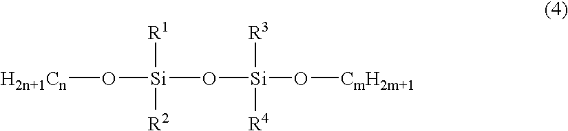
wherein R1, R2, R3 and R4 are one of CH3, C2H3, C2H5, C3H7 and C6H5, and m and n are any integer.

wherein R1, R2, R3, R4, R5 and R6 are one of CH3, C2H3, C2H5, C3H7 and C6H5, and the additive gases are argon (Ar), Helium (He) and either nitrogen oxide (N2O) or oxygen (O2).

wherein R1, R2, R3 and R4 are one of CH3, C2H3, C2H5, C3H7 and C6H5, and the additive gases are argon (Ar), Helium (He) and either nitrogen oxide (N2O) or oxygen (O2).
Rt[s]=9.42×10⁷(Pr·Ts/Ps·Tr)r w 2 d/F
-
- wherein:
- Pr: reaction chamber pressure (Pa)
- Ps: standard atmospheric pressure (Pa)
- Tr: average temperature of the reaction (K)
- Ts: standard temperature (K)
- rw: radius of the silicon substrate (m)
- d: space between the silicon substrate and the upper electrode (m)
- F: total flow volume of the reaction gas (sccm)

wherein X1 and X2 are OnCmHp wherein n is 0 or 1, m and p are integers including zero.
-
- rw (radius of the silicon substrate): 0.1 m
- d (space between the silicon substrate and the upper electrode): 0.024 m
- Ps (standard atmospheric pressure): 1.01×10⁵ Pa
- Ts (standard temperature): 273 K
-
- DMDMOS (dimethyl dimethoxysilane): 160 sccm
- IPA (isopropyl alcohol): 200 sccm
- He: 50 sccm
- Pr (reaction chamber pressure): 500 Pa
- RF power supply (HF: 13.4 MHz): 1600 W
- RF power supply (LF: 400 kHz): 200 W
- Tr (average temperature of the reaction): 673 K
- F (total flow volume of the reaction gas): 410 sccm
- Rt (residence time; Rt[s]=9.42×10⁷(Pr·Ts/Ps·Tr)rw 2d/F): 119 ms
-
- k (dielectric constant): 3.5
- Stress: −160 MPa
- Modulus: 35 GPa
- Hardness: 4.1 GPa
-
- DMDMOS (dimethyl dimethoxysilane): 160 sccm
- IPA (isopropyl alcohol): 0 sccm
- He: 150 sccm
- Pr (reaction chamber pressure): 533 Pa
- RF power supply (HF: 13.4 MHz): 1400 W
- RF power supply (LF: 400 kHz): 300 W
- Tr (average temperature of the reaction): 673 K
- F (total flow volume of the reaction gas): 310 sccm
- Rt (residence time; Rt[s]=9.42×10⁷(Pr·Ts/Ps·Tr)rw 2d/F): 168 ms
-
- k (dielectric constant): 3.4
- Stress: −180 MPa
- Modulus: 25 GPa
- Hardness: 3.1 GPa
-
- OMCTC (octamethylcyclotetrasiloxane): 160 sccm
- DVDVS ((CH3)2Si(C2H3)2): 80 sccm
- He: 100 sccm
- Pr (reaction chamber pressure): 467 Pa
- RF power supply (HF: 13.4 MHz): 1500 W
- RF power supply (LF: 400 kHz): 200 W
- Tr (average temperature of the reaction): 673 K
- F (total flow volume of the reaction gas): 340 sccm
- Rt (residence time; Rt[s]=9.42×10⁷(Pr·Ts/Ps·Tr)rw 2d/F): 120 ms
-
- k (dielectric constant): 3.5
- Stress: −190 MPa
- Modulus: 27 GPa
- Hardness: 3.3 GPa
-
- TMTVS ([CH2═CH(CH3)SiO]3): 140 sccm
- He: 100 sccm
- Pr (reaction chamber pressure): 360 Pa
- RF power supply (HF: 13.4 MHz): 200 W
- RF power supply (LF: 400 kHz): 50 W
- Tr (average temperature of the reaction): 673 K
- F (total flow volume of the reaction gas): 340 sccm
- Rt (residence time; Rt[s]=9.42×10⁷(Pr·Ts/Ps·Tr)rw 2d/F): 149 ms
-
- k (dielectric constant): 3.3
- Stress: −140 MPa
- Modulus: 23 GPa
- Hardness: 2.8 GPa
Rt[s]=9.42×10⁷(Pr·Ts/Ps·Tr)r w 2 d/F
-
- wherein Pr: reaction space pressure (Pa); Ps: standard atmospheric pressure (Pa); Tr: average temperature of the reaction (K); Ts: standard temperature (K); rw: radius of the silicon substrate (m); d: space between the silicon substrate and the upper electrode (m); F: total flow volume of the reaction gas (sccm).
Claims (31)
Rt[s]=9.42×10⁷(Pr·Ts/Ps·Tr)r w 2 d/F
Rt[s]=9.42×10⁷(Pr·Ts/Ps·Tr)r w 2 d/F
Rt[s]=9.42×10⁷(Pr·Ts/Ps·Tr)r w 2 d/F
Rt[s]=9.42×10⁷(Pr·Ts/Ps·Tr)r w 2 d/F
Priority Applications (4)
| Application Number | Priority Date | Filing Date | Title |
|---|---|---|---|
| US10/412,363 US7064088B2 (en) | 1998-02-05 | 2003-04-11 | Method for forming low-k hard film |
| US11/294,319 US7582575B2 (en) | 1998-02-05 | 2005-12-05 | Method for forming insulation film |
| US11/437,951 US20060258176A1 (en) | 1998-02-05 | 2006-05-19 | Method for forming insulation film |
| US11/465,751 US7354873B2 (en) | 1998-02-05 | 2006-08-18 | Method for forming insulation film |
Applications Claiming Priority (6)
| Application Number | Priority Date | Filing Date | Title |
|---|---|---|---|
| JP3792998 | 1998-02-05 | ||
| JP1998-37929 | 1998-02-05 | ||
| US24315699A | 1999-02-02 | 1999-02-02 | |
| US09/827,616 US6514880B2 (en) | 1998-02-05 | 2001-04-06 | Siloxan polymer film on semiconductor substrate and method for forming same |
| US10/317,239 US6881683B2 (en) | 1998-02-05 | 2002-12-11 | Insulation film on semiconductor substrate and method for forming same |
| US10/412,363 US7064088B2 (en) | 1998-02-05 | 2003-04-11 | Method for forming low-k hard film |
Related Parent Applications (1)
| Application Number | Title | Priority Date | Filing Date |
|---|---|---|---|
| US10/317,239 Continuation-In-Part US6881683B2 (en) | 1998-02-05 | 2002-12-11 | Insulation film on semiconductor substrate and method for forming same |
Related Child Applications (2)
| Application Number | Title | Priority Date | Filing Date |
|---|---|---|---|
| US11/294,319 Continuation-In-Part US7582575B2 (en) | 1998-02-05 | 2005-12-05 | Method for forming insulation film |
| US11/437,951 Continuation-In-Part US20060258176A1 (en) | 1998-02-05 | 2006-05-19 | Method for forming insulation film |
Publications (2)
| Publication Number | Publication Date |
|---|---|
| US20040038514A1 US20040038514A1 (en) | 2004-02-26 |
| US7064088B2 true US7064088B2 (en) | 2006-06-20 |
Family
ID=31892163
Family Applications (1)
| Application Number | Title | Priority Date | Filing Date |
|---|---|---|---|
| US10/412,363 Expired - Lifetime US7064088B2 (en) | 1998-02-05 | 2003-04-11 | Method for forming low-k hard film |
Country Status (1)
| Country | Link |
|---|---|
| US (1) | US7064088B2 (en) |
Cited By (40)
| Publication number | Priority date | Publication date | Assignee | Title |
|---|---|---|---|---|
| US20040253378A1 (en) * | 2003-06-12 | 2004-12-16 | Applied Materials, Inc. | Stress reduction of SIOC low k film by addition of alkylenes to OMCTS based processes |
| US20050037153A1 (en) * | 2003-08-14 | 2005-02-17 | Applied Materials, Inc. | Stress reduction of sioc low k films |
| US20060110931A1 (en) * | 1998-02-05 | 2006-05-25 | Asm Japan K.K. | Method for forming insulation film |
| US20060258176A1 (en) * | 1998-02-05 | 2006-11-16 | Asm Japan K.K. | Method for forming insulation film |
| US20070004204A1 (en) * | 1998-02-05 | 2007-01-04 | Asm Japan K.K. | Method for forming insulation film |
| US20070066086A1 (en) * | 2003-08-20 | 2007-03-22 | Asm Japan K.K. | Method of forming silicon-containing insulation film having low dielectric constant and low film stress |
| US7239017B1 (en) | 2003-09-24 | 2007-07-03 | Novellus Systems, Inc. | Low-k B-doped SiC copper diffusion barrier films |
| US7282438B1 (en) | 2004-06-15 | 2007-10-16 | Novellus Systems, Inc. | Low-k SiC copper diffusion barrier films |
| US20080076266A1 (en) * | 2006-09-21 | 2008-03-27 | Asm Japan K.K. | Method for forming insulation film having high density |
| US7390537B1 (en) | 2003-11-20 | 2008-06-24 | Novellus Systems, Inc. | Methods for producing low-k CDO films with low residual stress |
| US7420275B1 (en) | 2003-09-24 | 2008-09-02 | Novellus Systems, Inc. | Boron-doped SIC copper diffusion barrier films |
| US20080274627A1 (en) * | 2007-05-01 | 2008-11-06 | Shin-Etsu Chemical Co., Ltd. | Silicon-containing film, forming material, making method, and semiconductor device |
| US20080305648A1 (en) * | 2007-06-06 | 2008-12-11 | Asm Japan K.K. | Method for forming inorganic silazane-based dielectric film |
| US7473653B1 (en) | 2003-03-31 | 2009-01-06 | Novellus Systems, Inc. | Methods for producing low stress porous low-k dielectric materials using precursors with organic functional groups |
| US7622369B1 (en) | 2008-05-30 | 2009-11-24 | Asm Japan K.K. | Device isolation technology on semiconductor substrate |
| US7651959B2 (en) | 2007-12-03 | 2010-01-26 | Asm Japan K.K. | Method for forming silazane-based dielectric film |
| US7695765B1 (en) * | 2004-11-12 | 2010-04-13 | Novellus Systems, Inc. | Methods for producing low-stress carbon-doped oxide films with improved integration properties |
| US20100136789A1 (en) * | 2008-12-01 | 2010-06-03 | Air Products And Chemicals, Inc. | Dielectric Barrier Deposition Using Oxygen Containing Precursor |
| US20100143609A1 (en) * | 2008-12-09 | 2010-06-10 | Asm Japan K.K. | Method for forming low-carbon cvd film for filling trenches |
| US7737525B1 (en) | 2004-03-11 | 2010-06-15 | Novellus Systems, Inc. | Method for producing low-K CDO films |
| US20100174103A1 (en) * | 2007-02-14 | 2010-07-08 | Jsr Corporation | Material for forming silicon-containing film, and silicon-containing insulating film and method for forming the same |
| US7781351B1 (en) * | 2004-04-07 | 2010-08-24 | Novellus Systems, Inc. | Methods for producing low-k carbon doped oxide films with low residual stress |
| US20100261925A1 (en) * | 2007-07-10 | 2010-10-14 | Jsr Corporation | Method for producing silicon compound |
| US20110042789A1 (en) * | 2008-03-26 | 2011-02-24 | Jsr Corporation | Material for chemical vapor deposition, silicon-containing insulating film and method for production of the silicon-containing insulating film |
| US7906174B1 (en) | 2006-12-07 | 2011-03-15 | Novellus Systems, Inc. | PECVD methods for producing ultra low-k dielectric films using UV treatment |
| US7915166B1 (en) | 2007-02-22 | 2011-03-29 | Novellus Systems, Inc. | Diffusion barrier and etch stop films |
| US20110135557A1 (en) * | 2009-12-04 | 2011-06-09 | Vishwanathan Rangarajan | Hardmask materials |
| US7972976B1 (en) | 2005-01-31 | 2011-07-05 | Novellus Systems, Inc. | VLSI fabrication processes for introducing pores into dielectric materials |
| US8124522B1 (en) | 2008-04-11 | 2012-02-28 | Novellus Systems, Inc. | Reducing UV and dielectric diffusion barrier interaction through the modulation of optical properties |
| US8173537B1 (en) | 2007-03-29 | 2012-05-08 | Novellus Systems, Inc. | Methods for reducing UV and dielectric diffusion barrier interaction |
| US8637412B2 (en) | 2011-08-19 | 2014-01-28 | International Business Machines Corporation | Process to form an adhesion layer and multiphase ultra-low k dielectric material using PECVD |
| US9234276B2 (en) | 2013-05-31 | 2016-01-12 | Novellus Systems, Inc. | Method to obtain SiC class of films of desired composition and film properties |
| US9337068B2 (en) | 2012-12-18 | 2016-05-10 | Lam Research Corporation | Oxygen-containing ceramic hard masks and associated wet-cleans |
| US9837270B1 (en) | 2016-12-16 | 2017-12-05 | Lam Research Corporation | Densification of silicon carbide film using remote plasma treatment |
| US10002787B2 (en) | 2016-11-23 | 2018-06-19 | Lam Research Corporation | Staircase encapsulation in 3D NAND fabrication |
| US10211310B2 (en) | 2012-06-12 | 2019-02-19 | Novellus Systems, Inc. | Remote plasma based deposition of SiOC class of films |
| US10297442B2 (en) | 2013-05-31 | 2019-05-21 | Lam Research Corporation | Remote plasma based deposition of graded or multi-layered silicon carbide film |
| US10325773B2 (en) | 2012-06-12 | 2019-06-18 | Novellus Systems, Inc. | Conformal deposition of silicon carbide films |
| US10832904B2 (en) | 2012-06-12 | 2020-11-10 | Lam Research Corporation | Remote plasma based deposition of oxygen doped silicon carbide films |
| US11049716B2 (en) | 2015-04-21 | 2021-06-29 | Lam Research Corporation | Gap fill using carbon-based films |
Families Citing this family (20)
| Publication number | Priority date | Publication date | Assignee | Title |
|---|---|---|---|---|
| US6593247B1 (en) * | 1998-02-11 | 2003-07-15 | Applied Materials, Inc. | Method of depositing low k films using an oxidizing plasma |
| US6486082B1 (en) * | 2001-06-18 | 2002-11-26 | Applied Materials, Inc. | CVD plasma assisted lower dielectric constant sicoh film |
| US7025748B2 (en) * | 2001-11-08 | 2006-04-11 | Boston Scientific Scimed, Inc. | Sheath based blood vessel puncture locator and depth indicator |
| US20030194495A1 (en) * | 2002-04-11 | 2003-10-16 | Applied Materials, Inc. | Crosslink cyclo-siloxane compound with linear bridging group to form ultra low k dielectric |
| US6815373B2 (en) | 2002-04-16 | 2004-11-09 | Applied Materials Inc. | Use of cyclic siloxanes for hardness improvement of low k dielectric films |
| US7060330B2 (en) | 2002-05-08 | 2006-06-13 | Applied Materials, Inc. | Method for forming ultra low k films using electron beam |
| US6936551B2 (en) * | 2002-05-08 | 2005-08-30 | Applied Materials Inc. | Methods and apparatus for E-beam treatment used to fabricate integrated circuit devices |
| US7056560B2 (en) * | 2002-05-08 | 2006-06-06 | Applies Materials Inc. | Ultra low dielectric materials based on hybrid system of linear silicon precursor and organic porogen by plasma-enhanced chemical vapor deposition (PECVD) |
| US20040101632A1 (en) * | 2002-11-22 | 2004-05-27 | Applied Materials, Inc. | Method for curing low dielectric constant film by electron beam |
| JP4334844B2 (en) * | 2002-06-26 | 2009-09-30 | 東京エレクトロン株式会社 | Manufacturing method of groove structure for device |
| US6797643B2 (en) * | 2002-10-23 | 2004-09-28 | Applied Materials Inc. | Plasma enhanced CVD low k carbon-doped silicon oxide film deposition using VHF-RF power |
| US6897163B2 (en) * | 2003-01-31 | 2005-05-24 | Applied Materials, Inc. | Method for depositing a low dielectric constant film |
| WO2005004221A2 (en) * | 2003-07-08 | 2005-01-13 | Silecs Oy | Low-k-dielectric material |
| JP2005294333A (en) * | 2004-03-31 | 2005-10-20 | Semiconductor Process Laboratory Co Ltd | Film depositing method and semiconductor device |
| US7560144B2 (en) * | 2005-03-22 | 2009-07-14 | Asm Japan K.K. | Method of stabilizing film quality of low-dielectric constant film |
| US7674521B2 (en) * | 2005-07-27 | 2010-03-09 | International Business Machines Corporation | Materials containing voids with void size controlled on the nanometer scale |
| US20070134435A1 (en) * | 2005-12-13 | 2007-06-14 | Ahn Sang H | Method to improve the ashing/wet etch damage resistance and integration stability of low dielectric constant films |
| US7297376B1 (en) | 2006-07-07 | 2007-11-20 | Applied Materials, Inc. | Method to reduce gas-phase reactions in a PECVD process with silicon and organic precursors to deposit defect-free initial layers |
| US8741394B2 (en) | 2010-03-25 | 2014-06-03 | Novellus Systems, Inc. | In-situ deposition of film stacks |
| US20110244142A1 (en) * | 2010-03-30 | 2011-10-06 | Applied Materials, Inc. | Nitrogen doped amorphous carbon hardmask |
Citations (10)
| Publication number | Priority date | Publication date | Assignee | Title |
|---|---|---|---|---|
| US6352945B1 (en) | 1998-02-05 | 2002-03-05 | Asm Japan K.K. | Silicone polymer insulation film on semiconductor substrate and method for forming the film |
| US6383955B1 (en) | 1998-02-05 | 2002-05-07 | Asm Japan K.K. | Silicone polymer insulation film on semiconductor substrate and method for forming the film |
| EP1225194A2 (en) | 2001-01-17 | 2002-07-24 | Air Products And Chemicals, Inc. | Method of forming a dielectric interlayer film with organosilicon precursors |
| US6432846B1 (en) | 1999-02-02 | 2002-08-13 | Asm Japan K.K. | Silicone polymer insulation film on semiconductor substrate and method for forming the film |
| US6436822B1 (en) | 2000-11-20 | 2002-08-20 | Intel Corporation | Method for making a carbon doped oxide dielectric material |
| US6514880B2 (en) | 1998-02-05 | 2003-02-04 | Asm Japan K.K. | Siloxan polymer film on semiconductor substrate and method for forming same |
| US20030100175A1 (en) * | 2001-10-09 | 2003-05-29 | Mitsubishi Denki Kabushiki Kaisha | Low dielectric constant material, process for preparing the same, insulating film comprising the same and semiconductor device |
| US20030194880A1 (en) * | 2002-04-16 | 2003-10-16 | Applied Materials, Inc. | Use of cyclic siloxanes for hardness improvement |
| US20040137757A1 (en) * | 2003-01-13 | 2004-07-15 | Applied Materials, Inc. | Method and apparatus to improve cracking thresholds and mechanical properties of low-k dielectric material |
| US6818570B2 (en) * | 2002-03-04 | 2004-11-16 | Asm Japan K.K. | Method of forming silicon-containing insulation film having low dielectric constant and high mechanical strength |
-
2003
- 2003-04-11 US US10/412,363 patent/US7064088B2/en not_active Expired - Lifetime
Patent Citations (12)
| Publication number | Priority date | Publication date | Assignee | Title |
|---|---|---|---|---|
| US6352945B1 (en) | 1998-02-05 | 2002-03-05 | Asm Japan K.K. | Silicone polymer insulation film on semiconductor substrate and method for forming the film |
| US6383955B1 (en) | 1998-02-05 | 2002-05-07 | Asm Japan K.K. | Silicone polymer insulation film on semiconductor substrate and method for forming the film |
| US6410463B1 (en) | 1998-02-05 | 2002-06-25 | Asm Japan K.K. | Method for forming film with low dielectric constant on semiconductor substrate |
| US6455445B2 (en) | 1998-02-05 | 2002-09-24 | Asm Japan K.K. | Silicone polymer insulation film on semiconductor substrate and method for forming the film |
| US6514880B2 (en) | 1998-02-05 | 2003-02-04 | Asm Japan K.K. | Siloxan polymer film on semiconductor substrate and method for forming same |
| US6432846B1 (en) | 1999-02-02 | 2002-08-13 | Asm Japan K.K. | Silicone polymer insulation film on semiconductor substrate and method for forming the film |
| US6436822B1 (en) | 2000-11-20 | 2002-08-20 | Intel Corporation | Method for making a carbon doped oxide dielectric material |
| EP1225194A2 (en) | 2001-01-17 | 2002-07-24 | Air Products And Chemicals, Inc. | Method of forming a dielectric interlayer film with organosilicon precursors |
| US20030100175A1 (en) * | 2001-10-09 | 2003-05-29 | Mitsubishi Denki Kabushiki Kaisha | Low dielectric constant material, process for preparing the same, insulating film comprising the same and semiconductor device |
| US6818570B2 (en) * | 2002-03-04 | 2004-11-16 | Asm Japan K.K. | Method of forming silicon-containing insulation film having low dielectric constant and high mechanical strength |
| US20030194880A1 (en) * | 2002-04-16 | 2003-10-16 | Applied Materials, Inc. | Use of cyclic siloxanes for hardness improvement |
| US20040137757A1 (en) * | 2003-01-13 | 2004-07-15 | Applied Materials, Inc. | Method and apparatus to improve cracking thresholds and mechanical properties of low-k dielectric material |
Non-Patent Citations (3)
| Title |
|---|
| U.S. Appl. No. 10/317,239, filed Dec. 11, 2002, Matsuki et al. |
| U.S. Appl. No. 10/351,669, filed Jan. 24, 2003, Tsuji et al. |
| U.S. Appl. No. 10/402,109, filed Mar. 27, 2003, Matsuki et al. |
Cited By (61)
| Publication number | Priority date | Publication date | Assignee | Title |
|---|---|---|---|---|
| US7354873B2 (en) | 1998-02-05 | 2008-04-08 | Asm Japan K.K. | Method for forming insulation film |
| US7582575B2 (en) * | 1998-02-05 | 2009-09-01 | Asm Japan K.K. | Method for forming insulation film |
| US20060110931A1 (en) * | 1998-02-05 | 2006-05-25 | Asm Japan K.K. | Method for forming insulation film |
| US20060258176A1 (en) * | 1998-02-05 | 2006-11-16 | Asm Japan K.K. | Method for forming insulation film |
| US20070004204A1 (en) * | 1998-02-05 | 2007-01-04 | Asm Japan K.K. | Method for forming insulation film |
| US7473653B1 (en) | 2003-03-31 | 2009-01-06 | Novellus Systems, Inc. | Methods for producing low stress porous low-k dielectric materials using precursors with organic functional groups |
| US20090239390A1 (en) * | 2003-03-31 | 2009-09-24 | Novellus Systems, Inc. | Methods for producing low stress porous and cdo low-k dielectric materials using precursors with organic functional groups |
| US7923385B2 (en) | 2003-03-31 | 2011-04-12 | Novellus Systems, Inc. | Methods for producing low stress porous and CDO low-K dielectric materials using precursors with organic functional groups |
| US7799705B1 (en) | 2003-03-31 | 2010-09-21 | Novellus Systems, Inc. | Methods for producing low stress porous low-k dielectric materials using precursors with organic functional groups |
| US20040253378A1 (en) * | 2003-06-12 | 2004-12-16 | Applied Materials, Inc. | Stress reduction of SIOC low k film by addition of alkylenes to OMCTS based processes |
| US20050037153A1 (en) * | 2003-08-14 | 2005-02-17 | Applied Materials, Inc. | Stress reduction of sioc low k films |
| US7655577B2 (en) | 2003-08-20 | 2010-02-02 | Asm Japan K.K. | Method of forming silicon-containing insulation film having low dielectric constant and low film stress |
| US20070111540A1 (en) * | 2003-08-20 | 2007-05-17 | Asm Japan K.K. | Method of forming silicon-containing insulation film having low dielectric constant and low film stress |
| US20070066086A1 (en) * | 2003-08-20 | 2007-03-22 | Asm Japan K.K. | Method of forming silicon-containing insulation film having low dielectric constant and low film stress |
| US7842604B1 (en) | 2003-09-24 | 2010-11-30 | Novellus Systems, Inc. | Low-k b-doped SiC copper diffusion barrier films |
| US7420275B1 (en) | 2003-09-24 | 2008-09-02 | Novellus Systems, Inc. | Boron-doped SIC copper diffusion barrier films |
| US7239017B1 (en) | 2003-09-24 | 2007-07-03 | Novellus Systems, Inc. | Low-k B-doped SiC copper diffusion barrier films |
| US7390537B1 (en) | 2003-11-20 | 2008-06-24 | Novellus Systems, Inc. | Methods for producing low-k CDO films with low residual stress |
| US7737525B1 (en) | 2004-03-11 | 2010-06-15 | Novellus Systems, Inc. | Method for producing low-K CDO films |
| US7781351B1 (en) * | 2004-04-07 | 2010-08-24 | Novellus Systems, Inc. | Methods for producing low-k carbon doped oxide films with low residual stress |
| US7573061B1 (en) | 2004-06-15 | 2009-08-11 | Novellus Systems, Inc. | Low-k SiC copper diffusion barrier films |
| US7968436B1 (en) | 2004-06-15 | 2011-06-28 | Novellus Systems, Inc. | Low-K SiC copper diffusion barrier films |
| US7282438B1 (en) | 2004-06-15 | 2007-10-16 | Novellus Systems, Inc. | Low-k SiC copper diffusion barrier films |
| US7695765B1 (en) * | 2004-11-12 | 2010-04-13 | Novellus Systems, Inc. | Methods for producing low-stress carbon-doped oxide films with improved integration properties |
| US7972976B1 (en) | 2005-01-31 | 2011-07-05 | Novellus Systems, Inc. | VLSI fabrication processes for introducing pores into dielectric materials |
| US20080076266A1 (en) * | 2006-09-21 | 2008-03-27 | Asm Japan K.K. | Method for forming insulation film having high density |
| US7718553B2 (en) | 2006-09-21 | 2010-05-18 | Asm Japan K.K. | Method for forming insulation film having high density |
| US7906174B1 (en) | 2006-12-07 | 2011-03-15 | Novellus Systems, Inc. | PECVD methods for producing ultra low-k dielectric films using UV treatment |
| US20100174103A1 (en) * | 2007-02-14 | 2010-07-08 | Jsr Corporation | Material for forming silicon-containing film, and silicon-containing insulating film and method for forming the same |
| US8669181B1 (en) | 2007-02-22 | 2014-03-11 | Novellus Systems, Inc. | Diffusion barrier and etch stop films |
| US7915166B1 (en) | 2007-02-22 | 2011-03-29 | Novellus Systems, Inc. | Diffusion barrier and etch stop films |
| US8173537B1 (en) | 2007-03-29 | 2012-05-08 | Novellus Systems, Inc. | Methods for reducing UV and dielectric diffusion barrier interaction |
| US20080274627A1 (en) * | 2007-05-01 | 2008-11-06 | Shin-Etsu Chemical Co., Ltd. | Silicon-containing film, forming material, making method, and semiconductor device |
| US20080305648A1 (en) * | 2007-06-06 | 2008-12-11 | Asm Japan K.K. | Method for forming inorganic silazane-based dielectric film |
| US7781352B2 (en) | 2007-06-06 | 2010-08-24 | Asm Japan K.K. | Method for forming inorganic silazane-based dielectric film |
| US20100261925A1 (en) * | 2007-07-10 | 2010-10-14 | Jsr Corporation | Method for producing silicon compound |
| US7651959B2 (en) | 2007-12-03 | 2010-01-26 | Asm Japan K.K. | Method for forming silazane-based dielectric film |
| US20110042789A1 (en) * | 2008-03-26 | 2011-02-24 | Jsr Corporation | Material for chemical vapor deposition, silicon-containing insulating film and method for production of the silicon-containing insulating film |
| US8124522B1 (en) | 2008-04-11 | 2012-02-28 | Novellus Systems, Inc. | Reducing UV and dielectric diffusion barrier interaction through the modulation of optical properties |
| US20090298257A1 (en) * | 2008-05-30 | 2009-12-03 | Asm Japan K.K. | Device isolation technology on semiconductor substrate |
| US7622369B1 (en) | 2008-05-30 | 2009-11-24 | Asm Japan K.K. | Device isolation technology on semiconductor substrate |
| US20100136789A1 (en) * | 2008-12-01 | 2010-06-03 | Air Products And Chemicals, Inc. | Dielectric Barrier Deposition Using Oxygen Containing Precursor |
| US8637396B2 (en) | 2008-12-01 | 2014-01-28 | Air Products And Chemicals, Inc. | Dielectric barrier deposition using oxygen containing precursor |
| US20100143609A1 (en) * | 2008-12-09 | 2010-06-10 | Asm Japan K.K. | Method for forming low-carbon cvd film for filling trenches |
| US8765233B2 (en) | 2008-12-09 | 2014-07-01 | Asm Japan K.K. | Method for forming low-carbon CVD film for filling trenches |
| US8846525B2 (en) | 2009-12-04 | 2014-09-30 | Novellus Systems, Inc. | Hardmask materials |
| US8247332B2 (en) | 2009-12-04 | 2012-08-21 | Novellus Systems, Inc. | Hardmask materials |
| US20110135557A1 (en) * | 2009-12-04 | 2011-06-09 | Vishwanathan Rangarajan | Hardmask materials |
| US8637412B2 (en) | 2011-08-19 | 2014-01-28 | International Business Machines Corporation | Process to form an adhesion layer and multiphase ultra-low k dielectric material using PECVD |
| US10325773B2 (en) | 2012-06-12 | 2019-06-18 | Novellus Systems, Inc. | Conformal deposition of silicon carbide films |
| US11264234B2 (en) | 2012-06-12 | 2022-03-01 | Novellus Systems, Inc. | Conformal deposition of silicon carbide films |
| US10832904B2 (en) | 2012-06-12 | 2020-11-10 | Lam Research Corporation | Remote plasma based deposition of oxygen doped silicon carbide films |
| US10211310B2 (en) | 2012-06-12 | 2019-02-19 | Novellus Systems, Inc. | Remote plasma based deposition of SiOC class of films |
| US9337068B2 (en) | 2012-12-18 | 2016-05-10 | Lam Research Corporation | Oxygen-containing ceramic hard masks and associated wet-cleans |
| US9234276B2 (en) | 2013-05-31 | 2016-01-12 | Novellus Systems, Inc. | Method to obtain SiC class of films of desired composition and film properties |
| US10297442B2 (en) | 2013-05-31 | 2019-05-21 | Lam Research Corporation | Remote plasma based deposition of graded or multi-layered silicon carbide film |
| US10472714B2 (en) | 2013-05-31 | 2019-11-12 | Novellus Systems, Inc. | Method to obtain SiC class of films of desired composition and film properties |
| US11049716B2 (en) | 2015-04-21 | 2021-06-29 | Lam Research Corporation | Gap fill using carbon-based films |
| US10580690B2 (en) | 2016-11-23 | 2020-03-03 | Lam Research Corporation | Staircase encapsulation in 3D NAND fabrication |
| US10002787B2 (en) | 2016-11-23 | 2018-06-19 | Lam Research Corporation | Staircase encapsulation in 3D NAND fabrication |
| US9837270B1 (en) | 2016-12-16 | 2017-12-05 | Lam Research Corporation | Densification of silicon carbide film using remote plasma treatment |
Also Published As
| Publication number | Publication date |
|---|---|
| US20040038514A1 (en) | 2004-02-26 |
Similar Documents
| Publication | Publication Date | Title |
|---|---|---|
| US7064088B2 (en) | Method for forming low-k hard film | |
| US6881683B2 (en) | Insulation film on semiconductor substrate and method for forming same | |
| US6740602B1 (en) | Method of forming low-dielectric constant film on semiconductor substrate by plasma reaction using high-RF power | |
| US7582575B2 (en) | Method for forming insulation film | |
| US6352945B1 (en) | Silicone polymer insulation film on semiconductor substrate and method for forming the film | |
| US6432846B1 (en) | Silicone polymer insulation film on semiconductor substrate and method for forming the film | |
| US7354873B2 (en) | Method for forming insulation film | |
| US6852650B2 (en) | Insulation film on semiconductor substrate and method for forming same | |
| US6410463B1 (en) | Method for forming film with low dielectric constant on semiconductor substrate | |
| US7524735B1 (en) | Flowable film dielectric gap fill process | |
| US6514880B2 (en) | Siloxan polymer film on semiconductor substrate and method for forming same | |
| US6818570B2 (en) | Method of forming silicon-containing insulation film having low dielectric constant and high mechanical strength | |
| US20060258176A1 (en) | Method for forming insulation film | |
| US7655577B2 (en) | Method of forming silicon-containing insulation film having low dielectric constant and low film stress | |
| US6784123B2 (en) | Insulation film on semiconductor substrate and method for forming same | |
| US20080274627A1 (en) | Silicon-containing film, forming material, making method, and semiconductor device | |
| WO2001036703A1 (en) | System and method for depositing inorganic/organic dielectric films | |
| EP1396884A2 (en) | Interlayer insulation film used for multilayer interconnect of semiconductor integrated circuit and method of manufacturing the same | |
| US7585789B2 (en) | Method for forming porous insulation film | |
| JP3197007B2 (en) | Silicon polymer insulating film on semiconductor substrate and method for forming the film | |
| JP3781730B2 (en) | Method for forming silicon insulating film having low dielectric constant and high mechanical strength | |
| JP4651076B2 (en) | Method for forming an insulating film on a semiconductor substrate | |
| JP2002329718A (en) | Siloxane polymer film on semiconductor substrate and its manufacturing method |
Legal Events
| Date | Code | Title | Description |
|---|---|---|---|
| AS | Assignment |
Owner name: ASM JAPAN K.K., JAPAN Free format text: ASSIGNMENT OF ASSIGNORS INTEREST;ASSIGNORS:HYODO, YASUYOSHI;FUKAZAWA, ATSUKI;MORISADA, YOSHINORI;AND OTHERS;REEL/FRAME:014232/0698;SIGNING DATES FROM 20030507 TO 20030509 |
|
| STCF | Information on status: patent grant |
Free format text: PATENTED CASE |
|
| FEPP | Fee payment procedure |
Free format text: PAYER NUMBER DE-ASSIGNED (ORIGINAL EVENT CODE: RMPN); ENTITY STATUS OF PATENT OWNER: LARGE ENTITY Free format text: PAYOR NUMBER ASSIGNED (ORIGINAL EVENT CODE: ASPN); ENTITY STATUS OF PATENT OWNER: LARGE ENTITY |
|
| FPAY | Fee payment |
Year of fee payment: 4 |
|
| FPAY | Fee payment |
Year of fee payment: 8 |
|
| MAFP | Maintenance fee payment |
Free format text: PAYMENT OF MAINTENANCE FEE, 12TH YEAR, LARGE ENTITY (ORIGINAL EVENT CODE: M1553) Year of fee payment: 12 |