US7058455B2 - Interface for making spatially resolved electrical contact to neural cells in a biological neural network - Google Patents
Interface for making spatially resolved electrical contact to neural cells in a biological neural network Download PDFInfo
- Publication number
- US7058455B2 US7058455B2 US10/742,584 US74258403A US7058455B2 US 7058455 B2 US7058455 B2 US 7058455B2 US 74258403 A US74258403 A US 74258403A US 7058455 B2 US7058455 B2 US 7058455B2
- Authority
- US
- United States
- Prior art keywords
- interface
- channels
- layer
- membrane
- electrodes
- Prior art date
- Legal status (The legal status is an assumption and is not a legal conclusion. Google has not performed a legal analysis and makes no representation as to the accuracy of the status listed.)
- Expired - Lifetime, expires
Links
- 210000003061 neural cell Anatomy 0.000 title claims abstract description 50
- 238000013529 biological neural network Methods 0.000 title claims abstract description 26
- 239000012528 membrane Substances 0.000 claims abstract description 54
- 238000013528 artificial neural network Methods 0.000 claims abstract description 5
- 230000002207 retinal effect Effects 0.000 claims description 18
- 235000015097 nutrients Nutrition 0.000 claims description 14
- 230000005012 migration Effects 0.000 claims description 13
- 238000013508 migration Methods 0.000 claims description 13
- 238000000034 method Methods 0.000 claims description 11
- 230000003628 erosive effect Effects 0.000 claims description 6
- 210000004556 brain Anatomy 0.000 claims description 2
- 239000004065 semiconductor Substances 0.000 claims description 2
- 239000011148 porous material Substances 0.000 claims 4
- 230000001413 cellular effect Effects 0.000 claims 2
- 230000001939 inductive effect Effects 0.000 claims 1
- 210000004027 cell Anatomy 0.000 abstract description 69
- 230000005284 excitation Effects 0.000 abstract description 13
- 210000003050 axon Anatomy 0.000 abstract description 6
- 210000001525 retina Anatomy 0.000 description 21
- 210000001519 tissue Anatomy 0.000 description 12
- 239000000463 material Substances 0.000 description 9
- 230000001537 neural effect Effects 0.000 description 9
- 230000012292 cell migration Effects 0.000 description 8
- 230000012010 growth Effects 0.000 description 8
- 238000012545 processing Methods 0.000 description 8
- 230000015572 biosynthetic process Effects 0.000 description 6
- 230000005684 electric field Effects 0.000 description 6
- 238000013459 approach Methods 0.000 description 5
- 230000007423 decrease Effects 0.000 description 5
- 230000000694 effects Effects 0.000 description 5
- 238000004873 anchoring Methods 0.000 description 4
- 230000008901 benefit Effects 0.000 description 4
- 210000003169 central nervous system Anatomy 0.000 description 4
- 239000004205 dimethyl polysiloxane Substances 0.000 description 4
- 238000004519 manufacturing process Methods 0.000 description 4
- 229920000435 poly(dimethylsiloxane) Polymers 0.000 description 4
- 238000000926 separation method Methods 0.000 description 4
- 208000003098 Ganglion Cysts Diseases 0.000 description 3
- 208000005400 Synovial Cyst Diseases 0.000 description 3
- 238000000576 coating method Methods 0.000 description 3
- 238000010438 heat treatment Methods 0.000 description 3
- 108091008695 photoreceptors Proteins 0.000 description 3
- 230000008569 process Effects 0.000 description 3
- 230000009467 reduction Effects 0.000 description 3
- 230000004936 stimulating effect Effects 0.000 description 3
- 230000000638 stimulation Effects 0.000 description 3
- 201000004569 Blindness Diseases 0.000 description 2
- 229920002799 BoPET Polymers 0.000 description 2
- 102000004219 Brain-derived neurotrophic factor Human genes 0.000 description 2
- 108090000715 Brain-derived neurotrophic factor Proteins 0.000 description 2
- 108010005939 Ciliary Neurotrophic Factor Proteins 0.000 description 2
- 102100031614 Ciliary neurotrophic factor Human genes 0.000 description 2
- OHCQJHSOBUTRHG-KGGHGJDLSA-N FORSKOLIN Chemical compound O=C([C@@]12O)C[C@](C)(C=C)O[C@]1(C)[C@@H](OC(=O)C)[C@@H](O)[C@@H]1[C@]2(C)[C@@H](O)CCC1(C)C OHCQJHSOBUTRHG-KGGHGJDLSA-N 0.000 description 2
- 239000005041 Mylar™ Substances 0.000 description 2
- 230000003321 amplification Effects 0.000 description 2
- 239000000560 biocompatible material Substances 0.000 description 2
- 239000006229 carbon black Substances 0.000 description 2
- 239000011248 coating agent Substances 0.000 description 2
- 230000003247 decreasing effect Effects 0.000 description 2
- 230000005764 inhibitory process Effects 0.000 description 2
- 238000001459 lithography Methods 0.000 description 2
- 229910052751 metal Inorganic materials 0.000 description 2
- 239000002184 metal Substances 0.000 description 2
- 210000005036 nerve Anatomy 0.000 description 2
- 238000003199 nucleic acid amplification method Methods 0.000 description 2
- 210000001328 optic nerve Anatomy 0.000 description 2
- 238000002161 passivation Methods 0.000 description 2
- 230000035515 penetration Effects 0.000 description 2
- -1 polydimethylsiloxane Polymers 0.000 description 2
- 230000004222 uncontrolled growth Effects 0.000 description 2
- 210000004127 vitreous body Anatomy 0.000 description 2
- SUZLHDUTVMZSEV-UHFFFAOYSA-N Deoxycoleonol Natural products C12C(=O)CC(C)(C=C)OC2(C)C(OC(=O)C)C(O)C2C1(C)C(O)CCC2(C)C SUZLHDUTVMZSEV-UHFFFAOYSA-N 0.000 description 1
- 229910001218 Gallium arsenide Inorganic materials 0.000 description 1
- 208000017442 Retinal disease Diseases 0.000 description 1
- 208000007014 Retinitis pigmentosa Diseases 0.000 description 1
- 229910021607 Silver chloride Inorganic materials 0.000 description 1
- 206010064930 age-related macular degeneration Diseases 0.000 description 1
- 229940077737 brain-derived neurotrophic factor Drugs 0.000 description 1
- 230000015556 catabolic process Effects 0.000 description 1
- OHCQJHSOBUTRHG-UHFFFAOYSA-N colforsin Natural products OC12C(=O)CC(C)(C=C)OC1(C)C(OC(=O)C)C(O)C1C2(C)C(O)CCC1(C)C OHCQJHSOBUTRHG-UHFFFAOYSA-N 0.000 description 1
- 150000001875 compounds Chemical class 0.000 description 1
- 230000003412 degenerative effect Effects 0.000 description 1
- 238000006731 degradation reaction Methods 0.000 description 1
- HTXDPTMKBJXEOW-UHFFFAOYSA-N dioxoiridium Chemical compound O=[Ir]=O HTXDPTMKBJXEOW-UHFFFAOYSA-N 0.000 description 1
- 238000005516 engineering process Methods 0.000 description 1
- 210000003722 extracellular fluid Anatomy 0.000 description 1
- 239000000835 fiber Substances 0.000 description 1
- 210000000609 ganglia Anatomy 0.000 description 1
- 239000003102 growth factor Substances 0.000 description 1
- 238000005286 illumination Methods 0.000 description 1
- 229910010272 inorganic material Inorganic materials 0.000 description 1
- 239000011147 inorganic material Substances 0.000 description 1
- 239000012212 insulator Substances 0.000 description 1
- 238000011835 investigation Methods 0.000 description 1
- 229910000457 iridium oxide Inorganic materials 0.000 description 1
- 238000002955 isolation Methods 0.000 description 1
- 208000002780 macular degeneration Diseases 0.000 description 1
- 210000004126 nerve fiber Anatomy 0.000 description 1
- 210000002569 neuron Anatomy 0.000 description 1
- 150000004767 nitrides Chemical class 0.000 description 1
- 238000012856 packing Methods 0.000 description 1
- 230000000149 penetrating effect Effects 0.000 description 1
- 229920002120 photoresistant polymer Polymers 0.000 description 1
- 230000006461 physiological response Effects 0.000 description 1
- BASFCYQUMIYNBI-UHFFFAOYSA-N platinum Chemical compound [Pt] BASFCYQUMIYNBI-UHFFFAOYSA-N 0.000 description 1
- 229920000642 polymer Polymers 0.000 description 1
- 238000003672 processing method Methods 0.000 description 1
- 238000011160 research Methods 0.000 description 1
- HKZLPVFGJNLROG-UHFFFAOYSA-M silver monochloride Chemical compound [Cl-].[Ag+] HKZLPVFGJNLROG-UHFFFAOYSA-M 0.000 description 1
Images


Classifications
-
- A—HUMAN NECESSITIES
- A61—MEDICAL OR VETERINARY SCIENCE; HYGIENE
- A61B—DIAGNOSIS; SURGERY; IDENTIFICATION
- A61B5/00—Measuring for diagnostic purposes; Identification of persons
- A61B5/24—Detecting, measuring or recording bioelectric or biomagnetic signals of the body or parts thereof
- A61B5/25—Bioelectric electrodes therefor
- A61B5/279—Bioelectric electrodes therefor specially adapted for particular uses
- A61B5/291—Bioelectric electrodes therefor specially adapted for particular uses for electroencephalography [EEG]
-
- A—HUMAN NECESSITIES
- A61—MEDICAL OR VETERINARY SCIENCE; HYGIENE
- A61B—DIAGNOSIS; SURGERY; IDENTIFICATION
- A61B5/00—Measuring for diagnostic purposes; Identification of persons
- A61B5/24—Detecting, measuring or recording bioelectric or biomagnetic signals of the body or parts thereof
-
- A—HUMAN NECESSITIES
- A61—MEDICAL OR VETERINARY SCIENCE; HYGIENE
- A61N—ELECTROTHERAPY; MAGNETOTHERAPY; RADIATION THERAPY; ULTRASOUND THERAPY
- A61N1/00—Electrotherapy; Circuits therefor
- A61N1/02—Details
- A61N1/04—Electrodes
- A61N1/05—Electrodes for implantation or insertion into the body, e.g. heart electrode
- A61N1/0526—Head electrodes
- A61N1/0543—Retinal electrodes
-
- A—HUMAN NECESSITIES
- A61—MEDICAL OR VETERINARY SCIENCE; HYGIENE
- A61N—ELECTROTHERAPY; MAGNETOTHERAPY; RADIATION THERAPY; ULTRASOUND THERAPY
- A61N1/00—Electrotherapy; Circuits therefor
- A61N1/18—Applying electric currents by contact electrodes
- A61N1/32—Applying electric currents by contact electrodes alternating or intermittent currents
- A61N1/36—Applying electric currents by contact electrodes alternating or intermittent currents for stimulation
- A61N1/36046—Applying electric currents by contact electrodes alternating or intermittent currents for stimulation of the eye
Definitions
- the present invention relates generally to electrical stimulation or sensing of neural cells. More particularly, the present invention relates to an electrode configuration for selectively making electrical contact to neural cells.
- an approach for treating blindness caused by such conditions that has been under investigation for some time is provision of a retinal prosthesis connected to functional parts of the retina and providing photoreceptor functionality.
- a retinal prosthesis to functional parts of the retinal is typically accomplished with an array of electrodes (see, e.g., U.S. Pat. No. 4,628,933 to Michelson).
- Michelson teaches a regular array of bare electrodes in a “bed of nails” configuration, and also teaches a regular array of coaxial electrodes to reduce crosstalk between electrodes.
- the electrodes of Michelson can be positioned in close proximity to retinal cells to be stimulated, the electrode configurations of Michelson are not minimally invasive, and damage to functional parts of the retina may be difficult to avoid.
- U.S. Pat. No. 3,955,560 to Stein et al. is an example of an approach which provides low separation between electrodes and nerve fibers (i.e., axons), but requires a highly invasive procedure where a nerve is cut and then axons regenerate through a prosthesis and past electrodes embedded within the prosthesis.
- axons nerve fibers
- Still another objective of the present invention is to reduce cross-talk between neighboring electrodes.
- Another objective of the present invention is to ensure low threshold voltage and current for cell excitation.
- Yet another objective of the present invention is to provide an interface that allows for mechanical anchoring of neural tissue to a prosthesis.
- Still another objective of the present invention is to provide a large electrode surface area to decrease current density and thereby decrease the rate of electrochemical erosion.
- An advantage of the present invention is that a selected cell or group of neural cells can be brought into proximity to stimulating or sensing electrodes while preserving the signal processing functionality of a biological neural network.
- a further advantage of the present invention is that by bringing cells into close proximity to electrodes, electrical power required for cell excitation is reduced, thus decreasing tissue heating and electrode erosion.
- Another advantage of the present invention is that close proximity between cells and electrodes reduces cross-talk with non-selected cells, thus allowing a higher packing density of electrodes which provides improved spatial resolution.
- the present invention provides an interface for selective excitation or sensing of neural cells in a biological neural network.
- the interface includes a membrane with a number of channels passing through the membrane. Each channel has at least one electrode within it. Neural cells in the biological neural network grow or migrate into the channels, thereby coming into close proximity to the electrodes.
- a voltage applied to the electrode within the channel selectively excites the neural cell (or cells) in that channel.
- the excitation of these neural cell(s) will then transmit throughout the neural network (i.e., cells and axons) that is associated with the neural cell(s) stimulated in the channel.
- excitation of a neural cell (or cells) within the channel due to activity within the biological neural network is selectively sensed by the electrode within the channel.
- FIG. 1 shows an embodiment of the invention having a membrane with channels positioned under a retina.
- FIG. 2 shows an embodiment of the invention having a membrane with channels positioned under a retina, and having cells from the inner nuclear layer migrated into the channels.
- FIG. 3 shows a side view of an embodiment of the invention having a membrane with an electrode exposed inside the channel and coated outside the channel at the bottom of the membrane.
- FIG. 4 shows a bottom view of an embodiment of the invention according to FIG. 3 .
- FIG. 5 shows an embodiment of the invention having a membrane with channels positioned under a retina, and having neural cells migrated into the channels. Voltage applied to a channel electrode causes excitation of neural cells in that channel. The excited neural cells in that channel transmit signal(s) to the retinal network.
- FIG. 6 shows an embodiment of the invention having channels with two different channel diameters, and having a stop layer at the bottom to prevent cell migration past the channel while allowing nutrient flow.
- FIG. 7 shows an embodiment of an array according to the present invention.
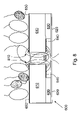
- FIG. 8 shows an embodiment of the invention where only a few (ideally one) neural cells can enter the channel. An electric field is applied across the cell providing efficient stimulation.
- FIG. 9 shows an embodiment of the invention having an electrode and/or an insulator laterally extending into a channel.
- FIG. 10 shows an embodiment of the invention having photosensitive circuitry connected to the electrodes, and having a perforated stop layer at the bottom to prevent cell migration past the channel while allowing nutrient flow.
- FIG. 1 shows an embodiment of the invention having a membrane 110 with a plurality of channels 120 passing through membrane 110 .
- membrane 110 is preferably positioned under a retina 130 .
- Exemplary retina 130 includes photoreceptors (i.e., rods and/or cones) 140 , inner nuclear layer cells 150 (e.g., bipolar cells), ganglion cells 160 and respective axons connecting to an optic nerve 170 .
- Membrane 110 can be of any type of biocompatible material that is substantially electrically non-conductive and is flexible enough to conform to the shape of the neural tissue in a biological neural network. Suitable materials for membrane 110 include mylar and PDMS (polydimethylsiloxane).
- the thickness of membrane 110 is less than 0.5 mm, and is preferably between about 5 microns and about 100 microns.
- Channels 120 pass completely through membrane 110 and can be of any shape, although substantially circular shapes are preferred.
- Retina 130 on FIG. 1 is an example of a biological neural network.
- the invention is applicable to making electrical contact to any kind of biological neural network, including but not limited to: central nervous system (CNS) neural networks (e.g., brain cortex), nuclei within the CNS, and nerve ganglia outside the CNS.
- CNS central nervous system
- a biological neural network is made up of interconnected biological processing elements (i.e., neurons) which respond in parallel to a set of input signals given to each.
- FIG. 2 shows cell migration into channels 120 of membrane 110 of FIG. 1 .
- membrane 110 When membrane 110 is positioned near a layer of neural tissue, neural cells in the neural tissue layer will tend to grow or migrate towards the channels. This growth process is a natural physiological response of cells and may depend on the existence of nutrients, space and a suitable surface morphology for these cells.
- a growth (or inhibition) factor could be included to enhance (or decrease) the migration or growth of the neural cells.
- growth or inhibition factor include but are not limited to: BDNF (brain-derived neurotrophic factor, CNTF (ciliary neurotrophic factor), Forskolin, Laminin, N-CAM and modified N-CAMs.
- BDNF brain-derived neurotrophic factor
- CNTF ciliary neurotrophic factor
- Forskolin Laminin
- N-CAM modified N-CAMs
- cells 210 are neural cells 150 which have migrated into and/or through channels 120 in membrane 110 positioned subretinally.
- the diameter of each channel should be sufficient to allow migration of neural cells 150 , and is preferably in a range from about 5 microns to about 20 microns.
- Penetration of neural cells 150 into and through channels 120 provides mechanical anchoring of retina 130 to membrane 110 .
- FIG. 3 shows an enlarged view of one of the channels of the configuration of FIG. 2 .
- an electrode 310 is positioned inside channel 120 in membrane 110 leaving enough space for neural cells 210 and their axons to migrate and grow through the channel. As a result of this cell migration, electrode 310 is in close proximity to neural cells 210 .
- Electrode 310 is shown extending to a bottom surface of membrane 110 (i.e., a surface of membrane 110 facing away from the biological neural network). Wires (not shown) can connect electrodes 310 to input and/or output terminals (not shown), or to circuitry within membrane 110 .
- a non-conductive layer 350 is preferably disposed on the bottom surface of membrane 110 covering electrodes 310 (and any wires, if present) to provide electrical isolation.
- FIG. 4 shows a view as seen looking up at non-conductive layer 350 of two channels 120 having the configuration of FIG. 3 .
- FIG. 4 also shows close proximity between electrodes 310 and cells 210 .
- Electrodes 310 are in electrical contact with neural cells 210 , but may or may not be in physical contact with neural cells 210 . Direct physical contact between electrodes 310 and cells 210 is not necessary for electrodes 310 to stimulate cells 210 , or for electrodes 310 to sense activity of cells 210 .
- FIG. 5 shows operation of the configuration of FIG. 2 .
- a selected neural cell (or cells) 510 within one of channels 120 is electrically excited by an electrode within the same channel.
- Impulses from neural cell (or cells) 510 excite selected ganglion cells 520 , which in turn excite selected optic nerve fibers 530 .
- Electrodes 310 and migrated cells 210 are provided, which reduces the electrical power required to stimulate cells 210 and decreases cross-talk to unselected cells (i.e., cells not within the channel 120 corresponding to a particular electrode 310 ). Reduction of electrical power required to stimulate cells 210 leads to reduced tissue heating and to reduced electrochemical erosion of electrodes 310 . Reduction of cross-talk to unselected cells provides improved spatial resolution. Furthermore, electrodes 310 are well insulated from each other by membrane 110 , so electrode to electrode cross-talk is also reduced. Additionally, the growth and/or migration of neural cells 150 into channels 120 preserves existing functionality of retina 130 .
- FIGS. 1–5 do not directly limit growth and/or migration of cells through channels 120 .
- Such uncontrolled tuft growth can lead to fusing of adjacent tufts, which tends to undesirably increase crosstalk.
- electrodes 310 have a small surface area, which increases current density and thus increases undesirable electrochemical activity at electrodes 310 .
- FIG. 6 shows an interface 600 according to an embodiment of the invention which prevents the formation of such uncontrolled retinal tufts and provides increased electrode surface area.
- a first layer 610 and a second layer 630 form a membrane analogous to membrane 110 of FIG. 1 .
- a channel passes through both first layer 610 and second layer 630 , where the channel diameter d 2 in second layer 630 is larger than the channel diameter d 1 in first layer 610 .
- the thickness of layers 610 and 630 together is less than 0.5 mm.
- the thickness of layer 610 is preferably between about 10 microns and about 50 microns.
- the thickness of layer 630 is preferably between about 5 microns and about 50 microns.
- a stop layer 620 is disposed such that second layer 630 is in between first layer 610 and stop layer 620 .
- Stop layer 620 is shown as having a hole with diameter d 3 aligned to the channel through layers 610 and 630 .
- An electrode 640 is disposed on a surface of first layer 610 facing second layer 630 .
- Layers 610 , 620 , and 630 can be of any type of biocompatible material that is substantially electrically non-conductive and is flexible enough to conform to the shape of the neural tissue in a biological neural network. Suitable materials include mylar and PDMS (polydimethylsiloxane).
- First layer 610 is in proximity to and faces a biological neural network (not shown on FIG. 6 ).
- Retina 130 as shown on FIG. 1 is an example of such a biological neural network.
- the diameter d 1 should be sufficiently large to allow migration of neural cells (such as 150 on FIG. 1 ), and is preferably in a range from about 5 microns to about 50 microns.
- stop layer 620 The function of stop layer 620 is to prevent uncontrolled growth of a retinal tuft past stop layer 620 , while permitting nutrients to flow to a cell (or cells) within the channel passing through layers 610 and 630 . Therefore, diameter d 3 should be small enough to prevent growth or migration of cells (or cell process) through stop layer 620 . Preferably, d 3 is less than about 5 microns in order to prevent cell migration through stop layer 620 .
- stop layer 620 can include several small holes each having a diameter of less than about 5 microns, where the holes in layer 620 are aligned with the channel within second layer 630 . More generally, stop layer 620 can be either an impermeable membrane having at least one hole in it large enough to permit nutrient flow and small enough to prevent cells from moving through it, or a membrane which is permeable to nutrient flow.
- a retinal tuft may form within the channel through second layer 630 .
- Such retinal tuft formation is not uncontrolled, since the maximum size of the retinal tuft is determined by stop layer 620 .
- controlled retinal tuft formation is likely to be desirable, since it will tend to provide improved mechanical anchoring of interface 600 to a retina.
- Electrode 640 is disposed on a surface of first layer 610 facing second layer 630 and within the channel passing through the two layers. Since d 2 is greater than d 1 , the surface area of electrode 640 can be made significantly larger than the area of an electrode within a channel having a uniform channel diameter along its length (such as shown on FIG. 3 ). The diameter d 2 is preferably from about 10 microns to about 100 microns.
- an electrode 650 is disposed on the top surface of first layer 610 . An applied voltage between electrodes 640 and 650 provides an electric field within the channel passing through first layer 610 .
- One variation of the present invention is to coat electrode 640 to further increase its surface area and to further decrease the current density and associated rate of electrochemical erosion of the conductive layer.
- carbon black has a surface area of about 1000 m 2 /g and so a coating of carbon black on electrode 640 can significantly increase its effective surface area.
- suitable materials for such a coating include platinum black, iridium oxide, and silver chloride.
- Laser processing can be used to form channels.
- the largest holes i.e. the channels through second layer 630
- layers 630 and 610 are attached to each other.
- the next largest holes are then formed, using the previously formed holes for alignment, and stop layer 620 is then attached to second layer 630 .
- the smallest holes are formed in stop layer 620 , using previously formed holes for alignment.
- Electrodes 640 on first layer 610 can also be formed by laser processing.
- first layer 610 can have a continuous film of metal deposited on the surface of layer 610 that will eventually face toward second layer 630 , and laser processing of this continuous film of metal can define electrodes 640 (and optionally wires connected to these electrodes as discussed in connection with FIG. 3 ). Laser processing methods to perform these tasks are known in the art.
- FIG. 7 shows an interface 700 including several interfaces 600 (shown as 600 a , 600 b , 600 c , etc.) according to FIG. 6 , for making selective contact to multiple points in a retina.
- interfaces 600 within interface 700 are arranged as a two-dimensional array, where each channel corresponds to a pixel of the array.
- electrode 650 is preferably a common electrode for all channels. Resistance between electrodes 640 corresponding to different array elements is largely determined by the diameter d 3 of the hole in stop layer 620 , since conduction is mainly through extra cellular fluid surrounding interfaces 600 .
- the selection of d 3 (or equivalently, the total open area in stop layer 620 ) is determined by a tradeoff between reducing electrode to electrode cross-talk (by decreasing d 3 ) and providing sufficient nutrient flow (by increasing d 3 ).
- FIG. 9 shows operation of an interface 900 which is a variation of interface 600 .
- electrode 640 and/or an insulating intermediate layer 920 is/are extended partway into the channel passing through first layer 610 .
- the example of FIG. 9 shows both electrode 640 and intermediate layer 920 extending into the channel.
- Such reduction of the minimum channel diameter reduces the electrical power required to excite cell 820 , because the impedance of electrode 640 increases.
- a part of the cell 820 located close to the small opening in electrode 640 and intermediate layer 920 will be depolarized.
- Extension of electrode 640 in this manner also further increases its surface area, which desirably reduces the rate of electrochemical erosion of electrode 640 .
- FIG. 10 shows operation of an interface 1000 according to another embodiment of the invention.
- a first layer 1010 and a second layer 1020 form a membrane analogous to membrane 110 of FIG. 1 .
- a channel passes through both first layer 1010 and second layer 1020 , where the channel diameter in second layer 1020 is larger than the channel diameter in first layer 1010 .
- the thickness of layers 1010 and 1020 together is less than 0.5 mm.
- the thickness of second layer 1020 is on the order of several times a typical cell dimension, to provide room for formation of a controlled retinal tuft within second layer 1020 .
- Layer 1010 preferably has a thickness between about 5 microns and about 50 microns.
- Layer 1020 preferably has a thickness between about 5 microns and about 100 microns.
- a stop layer 1030 is disposed such that second layer 1020 is in between first layer 1010 and stop layer 1030 .
- stop layer 1030 The function of stop layer 1030 is to prevent uncontrolled growth of a retinal tuft past stop layer 1030 , while permitting nutrients to flow to a cell (or cells) within the channel passing through layers 1010 and 1020 .
- Stop layer 1030 is shown as having several small holes aligned to the channel through layer 1020 . Preferably, these holes each have a diameter of less than about 5 microns, to prevent cell migration through the holes.
- stop layer 1030 could have a single small hole per channel, as shown on FIG. 6 . More generally, stop layer 1030 can be either an impermeable membrane having at least one hole in it large enough to permit nutrient flow and small enough to prevent cells from moving through it, or a membrane which is permeable to nutrient flow.
- An electrode 1090 is disposed on a surface of first layer 1010 facing second layer 1020
- another electrode 1080 is disposed on a surface of first layer 1010 facing away from second layer 1020
- a photo-sensitive circuit 1070 e.g., a photodiode, a phototransistor, etc.
- Electrode 1080 is preferably transparent to light and/or patterned in such a way that allows for light penetration to photo-sensitive circuit 1070 .
- FIG. 10 provides photo-sensitive circuit 1070 connected to electrodes 1080 and 1090 .
- layer 1010 it is preferable for layer 1010 to be fabricated from a light-sensitive material permitting fabrication of photo-sensitive circuitry 1070 (e.g., any of various compound semiconductors such as GaAs and the like).
- layers 1020 and 1030 it is convenient for layers 1020 and 1030 to be materials compatible with the processing technology of the material of layer 1010 .
- layers 1020 and 1030 can be polymers (e.g., photoresists) or inorganic materials (e.g., oxides or nitrides).
- Channels through layers 1010 and 1020 are preferably formed via lithography, in order to enable rapid fabrication of devices having a large number of channels. Since the materials indicated above are not typically bio-compatible, biological passivation of embodiments of the invention made with such materials is preferred. Suitable biological passivation techniques for such materials are known in the art.
- amplification circuitry (not shown) to increase the signal at electrodes 1080 and 1090 responsive to illumination of photo-sensitive circuit 1070 .
- the potential difference between electrodes 1080 and 1090 provides an electric field 1040 passing through a cell 1050 within the channel. Excitation of cell 1050 by electric field 1040 provides selective excitation of the retina, as shown on FIG. 5 .
- additional perforations can be included in the membrane to assist and/or ensure flow of nutrients.
- the diameter of such perforations should be smaller than the diameter of the channels to avoid neural cell migration through these additional perforations (i.e., tuft formation), but large enough to ensure a flow of nutrients.
- Specific growth factor(s) or surface coatings can be used to ensure migration of a particular cell group, e.g. only bipolar cells, or even a specific type of bipolar cell (e.g., “on” or “off” cells).
- the interface can have some channels or perforations for stimulation purposes while other channels or perforations can be designed for mechanical anchoring to neural tissue
- the interface has been discussed in light of electrically stimulating a select group of neural cells, however, the interface could also be used to measure signals generated in neural cells due to an external trigger/excitation, for example, signals generated in retinal cells due to light excitation.
- FIG. 10 a preferred lithographic fabrication approach for the embodiment of FIG. 10 was discussed.
- laser processing was discussed in connection with the embodiment of FIG. 6 .
- the invention is not limited to any one fabrication method.
- the use of lithography is not restricted to the embodiment of FIG. 10 .
- the use of laser processing is not restricted to the embodiment of FIG. 6 .
Abstract
Description
Claims (31)
Priority Applications (6)
| Application Number | Priority Date | Filing Date | Title |
|---|---|---|---|
| US10/742,584 US7058455B2 (en) | 2003-02-14 | 2003-12-19 | Interface for making spatially resolved electrical contact to neural cells in a biological neural network |
| EP04704495A EP1599251A2 (en) | 2003-02-14 | 2004-01-22 | Interface for making spatially resolved electrical contact to neural cells in a biological neural network |
| CA002515833A CA2515833A1 (en) | 2003-02-14 | 2004-01-22 | Interface for making spatially resolved electrical contact to neural cells in a biological neural network |
| PCT/US2004/002038 WO2004073785A2 (en) | 2003-02-14 | 2004-01-22 | Perforated electrode array for neural stimulation |
| JP2006503000A JP2006517829A (en) | 2003-02-14 | 2004-01-22 | An interface that allows a spatial resolution current to flow selectively to multiple neurons in a biological neural network |
| US11/035,692 US20050203601A1 (en) | 2003-02-14 | 2005-01-13 | Neural stimulation array providing proximity of electrodes to cells via cellular migration |
Applications Claiming Priority (3)
| Application Number | Priority Date | Filing Date | Title |
|---|---|---|---|
| US44742103P | 2003-02-14 | 2003-02-14 | |
| US44779603P | 2003-02-14 | 2003-02-14 | |
| US10/742,584 US7058455B2 (en) | 2003-02-14 | 2003-12-19 | Interface for making spatially resolved electrical contact to neural cells in a biological neural network |
Related Child Applications (1)
| Application Number | Title | Priority Date | Filing Date |
|---|---|---|---|
| US11/035,692 Continuation-In-Part US20050203601A1 (en) | 2003-02-14 | 2005-01-13 | Neural stimulation array providing proximity of electrodes to cells via cellular migration |
Publications (2)
| Publication Number | Publication Date |
|---|---|
| US20040230270A1 US20040230270A1 (en) | 2004-11-18 |
| US7058455B2 true US7058455B2 (en) | 2006-06-06 |
Family
ID=32913026
Family Applications (1)
| Application Number | Title | Priority Date | Filing Date |
|---|---|---|---|
| US10/742,584 Expired - Lifetime US7058455B2 (en) | 2003-02-14 | 2003-12-19 | Interface for making spatially resolved electrical contact to neural cells in a biological neural network |
Country Status (5)
| Country | Link |
|---|---|
| US (1) | US7058455B2 (en) |
| EP (1) | EP1599251A2 (en) |
| JP (1) | JP2006517829A (en) |
| CA (1) | CA2515833A1 (en) |
| WO (1) | WO2004073785A2 (en) |
Cited By (22)
| Publication number | Priority date | Publication date | Assignee | Title |
|---|---|---|---|---|
| US8428740B2 (en) | 2010-08-06 | 2013-04-23 | Nano-Retina, Inc. | Retinal prosthesis techniques |
| US8442641B2 (en) | 2010-08-06 | 2013-05-14 | Nano-Retina, Inc. | Retinal prosthesis techniques |
| US8571669B2 (en) | 2011-02-24 | 2013-10-29 | Nano-Retina, Inc. | Retinal prosthesis with efficient processing circuits |
| US20130317582A1 (en) * | 2012-05-24 | 2013-11-28 | National Chiao Tung University | Device for stimulating neural regeneration and fabrication method thereof |
| US8706243B2 (en) | 2009-02-09 | 2014-04-22 | Rainbow Medical Ltd. | Retinal prosthesis techniques |
| US8718784B2 (en) | 2010-01-14 | 2014-05-06 | Nano-Retina, Inc. | Penetrating electrodes for retinal stimulation |
| US9265945B2 (en) | 2009-02-09 | 2016-02-23 | Nano-Retina, Inc. | Retinal prosthesis |
| US9331791B2 (en) | 2014-01-21 | 2016-05-03 | Nano Retina Ltd. | Transfer of power and data |
| WO2016069874A1 (en) * | 2014-10-31 | 2016-05-06 | Board Of Regents, The University Of Texas System | Microchannel scaffolds and microtube electrodes for a neural interface system |
| US9370417B2 (en) | 2013-03-14 | 2016-06-21 | Nano-Retina, Inc. | Foveated retinal prosthesis |
| US9474902B2 (en) | 2013-12-31 | 2016-10-25 | Nano Retina Ltd. | Wearable apparatus for delivery of power to a retinal prosthesis |
| US9731118B2 (en) | 2011-04-05 | 2017-08-15 | Pedro Galvan-Garcia | Annular electrode array |
| US10016600B2 (en) | 2013-05-30 | 2018-07-10 | Neurostim Solutions, Llc | Topical neurological stimulation |
| US10953225B2 (en) | 2017-11-07 | 2021-03-23 | Neurostim Oab, Inc. | Non-invasive nerve activator with adaptive circuit |
| US11077301B2 (en) | 2015-02-21 | 2021-08-03 | NeurostimOAB, Inc. | Topical nerve stimulator and sensor for bladder control |
| US11229789B2 (en) | 2013-05-30 | 2022-01-25 | Neurostim Oab, Inc. | Neuro activator with controller |
| US11305118B2 (en) | 2018-11-30 | 2022-04-19 | Biovisics Medical, Inc. | Head worn apparatuses for vision therapy |
| US11338139B2 (en) | 2018-10-01 | 2022-05-24 | Biovisics Medical, Inc. | System and methods for controlled electrical modulation for vision therapy |
| US11458311B2 (en) | 2019-06-26 | 2022-10-04 | Neurostim Technologies Llc | Non-invasive nerve activator patch with adaptive circuit |
| US11471680B2 (en) | 2019-04-10 | 2022-10-18 | Biovisics, Inc. | Systems and interfaces for ocular therapy |
| US11511112B2 (en) | 2019-06-14 | 2022-11-29 | Biovisics Medical, Inc. | Wearable medical device |
| US11730958B2 (en) | 2019-12-16 | 2023-08-22 | Neurostim Solutions, Llc | Non-invasive nerve activator with boosted charge delivery |
Families Citing this family (9)
| Publication number | Priority date | Publication date | Assignee | Title |
|---|---|---|---|---|
| US20060224212A1 (en) * | 2005-04-01 | 2006-10-05 | Kennedy Philip R | Neural electrode array |
| US20060247753A1 (en) * | 2005-04-29 | 2006-11-02 | Wenger William K | Subcutaneous lead fixation mechanisms |
| EP1743665B1 (en) * | 2005-07-15 | 2015-03-11 | Imec | Neurotransmitter stimulation of neurons with feedback from sensors |
| US20080221645A1 (en) * | 2007-03-06 | 2008-09-11 | Neural Signals, Inc. | Neurotrophic Electrode Neural Interface Employing Quantum Dots |
| WO2008122044A2 (en) * | 2007-04-02 | 2008-10-09 | Georgia Tech Research Corporation | Implantable device for communicating with biological tissue |
| US7905013B2 (en) * | 2007-06-04 | 2011-03-15 | Sharp Laboratories Of America, Inc. | Method for forming an iridium oxide (IrOx) nanowire neural sensor array |
| GB0800797D0 (en) * | 2008-01-16 | 2008-02-27 | Cambridge Entpr Ltd | Neural interface |
| EP3494877B1 (en) | 2017-12-11 | 2024-02-07 | Nmi Naturwissenschaftliches Und Medizinisches Institut An Der Universität Tübingen | Device for the examination of neurons |
| US20140279772A1 (en) * | 2013-03-13 | 2014-09-18 | Baker Hughes Incorporated | Neuronal networks for controlling downhole processes |
Citations (11)
| Publication number | Priority date | Publication date | Assignee | Title |
|---|---|---|---|---|
| US3955560A (en) | 1974-06-10 | 1976-05-11 | Stein Richard B | Implantable neural electrode |
| US4628933A (en) | 1985-07-23 | 1986-12-16 | Michelson Robin P | Method and apparatus for visual prosthesis |
| US5109844A (en) | 1990-10-11 | 1992-05-05 | Duke University | Retinal microstimulation |
| US5575813A (en) * | 1992-09-11 | 1996-11-19 | Massachusetts Institute Of Technology | Low-pressure neural contact structure |
| US6032062A (en) | 1995-08-10 | 2000-02-29 | Nmi Naturwissenschaftliches Und Medizinisches Institut | Microelectrode arrangement |
| US6324429B1 (en) | 1998-05-08 | 2001-11-27 | Massachusetts Eye And Ear Infirmary | Chronically implantable retinal prosthesis |
| US6347250B1 (en) | 1996-10-23 | 2002-02-12 | Nmi Univ Tuebingen | Optically controllable microelectrode array for stimulating cells within a tissue |
| US6393327B1 (en) | 2000-08-09 | 2002-05-21 | The United States Of America As Represented By The Secretary Of The Navy | Microelectronic stimulator array |
| US20020169486A1 (en) | 2000-05-04 | 2002-11-14 | Optobionics Corporation | Artificial retina device with stimulating and ground return electrodes disposed on opposite sides of the neuroretina and method of attachment |
| US20030032946A1 (en) | 2001-06-29 | 2003-02-13 | Fishman Harvey A. | Artificial synapse chip interface for electronic prosthetic retina |
| US20050203601A1 (en) * | 2003-02-14 | 2005-09-15 | Daniel Palanker | Neural stimulation array providing proximity of electrodes to cells via cellular migration |
Family Cites Families (1)
| Publication number | Priority date | Publication date | Assignee | Title |
|---|---|---|---|---|
| US3955590A (en) * | 1974-11-05 | 1976-05-11 | Midland-Ross Corporation | Regulator for vehicle leveling systems |
-
2003
- 2003-12-19 US US10/742,584 patent/US7058455B2/en not_active Expired - Lifetime
-
2004
- 2004-01-22 EP EP04704495A patent/EP1599251A2/en not_active Withdrawn
- 2004-01-22 CA CA002515833A patent/CA2515833A1/en not_active Abandoned
- 2004-01-22 JP JP2006503000A patent/JP2006517829A/en not_active Withdrawn
- 2004-01-22 WO PCT/US2004/002038 patent/WO2004073785A2/en active Search and Examination
Patent Citations (11)
| Publication number | Priority date | Publication date | Assignee | Title |
|---|---|---|---|---|
| US3955560A (en) | 1974-06-10 | 1976-05-11 | Stein Richard B | Implantable neural electrode |
| US4628933A (en) | 1985-07-23 | 1986-12-16 | Michelson Robin P | Method and apparatus for visual prosthesis |
| US5109844A (en) | 1990-10-11 | 1992-05-05 | Duke University | Retinal microstimulation |
| US5575813A (en) * | 1992-09-11 | 1996-11-19 | Massachusetts Institute Of Technology | Low-pressure neural contact structure |
| US6032062A (en) | 1995-08-10 | 2000-02-29 | Nmi Naturwissenschaftliches Und Medizinisches Institut | Microelectrode arrangement |
| US6347250B1 (en) | 1996-10-23 | 2002-02-12 | Nmi Univ Tuebingen | Optically controllable microelectrode array for stimulating cells within a tissue |
| US6324429B1 (en) | 1998-05-08 | 2001-11-27 | Massachusetts Eye And Ear Infirmary | Chronically implantable retinal prosthesis |
| US20020169486A1 (en) | 2000-05-04 | 2002-11-14 | Optobionics Corporation | Artificial retina device with stimulating and ground return electrodes disposed on opposite sides of the neuroretina and method of attachment |
| US6393327B1 (en) | 2000-08-09 | 2002-05-21 | The United States Of America As Represented By The Secretary Of The Navy | Microelectronic stimulator array |
| US20030032946A1 (en) | 2001-06-29 | 2003-02-13 | Fishman Harvey A. | Artificial synapse chip interface for electronic prosthetic retina |
| US20050203601A1 (en) * | 2003-02-14 | 2005-09-15 | Daniel Palanker | Neural stimulation array providing proximity of electrodes to cells via cellular migration |
Non-Patent Citations (7)
| Title |
|---|
| Boppart et al., "A Flexible Perforated Microelectrode Array for Extended Neural Recordings," IEEE Transactions on Biomedical Engineering, vol. 39, No. 1, pp. 37-42, Jan. 1992. |
| Huie et al., "Perforated Membrane as an Interface for Focal Electrical Stimulation of Retina," Investigative Ophthalmology & Visual Science 2003; 44: E-Abstract 5055. |
| Huie et al., "Tissue-engineered Neurite Conduits to Connect Retinal Ganglion Cells to an Electronic Retinal Prosthesis," Investigative Ophthalmology & Visual Science 2002; 43: E-Abstract 4475. |
| Kovacs et al., "Regeneration Microelectrode Array for Peripheral Nerve Recording and Stimulation," IEEE Transactions on Biomedical Engineering, vol. 39, No. 9, pp. 893-902 Sep. 1992. |
| Lars Wallman et al., "Perforated Silicon Nerve Chips with Doped Registration Electrodes: in Vitro Performance and in Vivo Operation," IEEE Transactions on Biomedical Engineering, vol. 46, No. 9, Sep. 1999. |
| Stephen A. Boppart et al., "A Flexible Perforated Microelectrode Array for Extended Neural Recordings," IEEE Transactions on Biomedical Engineering, vol. 39, No. 1, Jan. 1992. |
| Wallman et al., "Perforated Silicon Nerve Chips with Doped Registration Electrodes: in Vitro Performance and in Vivo Operation," IEEE Transactions on Biomedical Engineering, vol. 46 No. 9 pp. 1065-1073 Sep. 1999. |
Cited By (31)
| Publication number | Priority date | Publication date | Assignee | Title |
|---|---|---|---|---|
| US9198753B2 (en) | 2009-02-09 | 2015-12-01 | Nano-Retina Inc. | Techniques for powering a retinal prosthesis |
| US9907969B2 (en) | 2009-02-09 | 2018-03-06 | Nano-Retina, Inc. | Retinal prosthesis with an external power source |
| US9566191B2 (en) | 2009-02-09 | 2017-02-14 | Nano-Retina, Inc. | Retinal prosthesis with visible-light filter |
| US8706243B2 (en) | 2009-02-09 | 2014-04-22 | Rainbow Medical Ltd. | Retinal prosthesis techniques |
| US9265945B2 (en) | 2009-02-09 | 2016-02-23 | Nano-Retina, Inc. | Retinal prosthesis |
| US8718784B2 (en) | 2010-01-14 | 2014-05-06 | Nano-Retina, Inc. | Penetrating electrodes for retinal stimulation |
| US8442641B2 (en) | 2010-08-06 | 2013-05-14 | Nano-Retina, Inc. | Retinal prosthesis techniques |
| US8428740B2 (en) | 2010-08-06 | 2013-04-23 | Nano-Retina, Inc. | Retinal prosthesis techniques |
| US9192464B2 (en) | 2011-02-24 | 2015-11-24 | Nano-Retina, Inc. | Retinal prosthesis with efficient processing circuits |
| US8571669B2 (en) | 2011-02-24 | 2013-10-29 | Nano-Retina, Inc. | Retinal prosthesis with efficient processing circuits |
| US9731118B2 (en) | 2011-04-05 | 2017-08-15 | Pedro Galvan-Garcia | Annular electrode array |
| US20130317582A1 (en) * | 2012-05-24 | 2013-11-28 | National Chiao Tung University | Device for stimulating neural regeneration and fabrication method thereof |
| US9108042B2 (en) * | 2012-05-24 | 2015-08-18 | National Chiao Tung University | Device for stimulating neural regeneration and fabrication method thereof |
| US9370417B2 (en) | 2013-03-14 | 2016-06-21 | Nano-Retina, Inc. | Foveated retinal prosthesis |
| US10918853B2 (en) | 2013-05-30 | 2021-02-16 | Neurostim Solutions, Llc | Topical neurological stimulation |
| US11229789B2 (en) | 2013-05-30 | 2022-01-25 | Neurostim Oab, Inc. | Neuro activator with controller |
| US11291828B2 (en) | 2013-05-30 | 2022-04-05 | Neurostim Solutions LLC | Topical neurological stimulation |
| US10016600B2 (en) | 2013-05-30 | 2018-07-10 | Neurostim Solutions, Llc | Topical neurological stimulation |
| US10307591B2 (en) | 2013-05-30 | 2019-06-04 | Neurostim Solutions, Llc | Topical neurological stimulation |
| US10946185B2 (en) | 2013-05-30 | 2021-03-16 | Neurostim Solutions, Llc | Topical neurological stimulation |
| US9474902B2 (en) | 2013-12-31 | 2016-10-25 | Nano Retina Ltd. | Wearable apparatus for delivery of power to a retinal prosthesis |
| US9331791B2 (en) | 2014-01-21 | 2016-05-03 | Nano Retina Ltd. | Transfer of power and data |
| WO2016069874A1 (en) * | 2014-10-31 | 2016-05-06 | Board Of Regents, The University Of Texas System | Microchannel scaffolds and microtube electrodes for a neural interface system |
| US11077301B2 (en) | 2015-02-21 | 2021-08-03 | NeurostimOAB, Inc. | Topical nerve stimulator and sensor for bladder control |
| US10953225B2 (en) | 2017-11-07 | 2021-03-23 | Neurostim Oab, Inc. | Non-invasive nerve activator with adaptive circuit |
| US11338139B2 (en) | 2018-10-01 | 2022-05-24 | Biovisics Medical, Inc. | System and methods for controlled electrical modulation for vision therapy |
| US11305118B2 (en) | 2018-11-30 | 2022-04-19 | Biovisics Medical, Inc. | Head worn apparatuses for vision therapy |
| US11471680B2 (en) | 2019-04-10 | 2022-10-18 | Biovisics, Inc. | Systems and interfaces for ocular therapy |
| US11511112B2 (en) | 2019-06-14 | 2022-11-29 | Biovisics Medical, Inc. | Wearable medical device |
| US11458311B2 (en) | 2019-06-26 | 2022-10-04 | Neurostim Technologies Llc | Non-invasive nerve activator patch with adaptive circuit |
| US11730958B2 (en) | 2019-12-16 | 2023-08-22 | Neurostim Solutions, Llc | Non-invasive nerve activator with boosted charge delivery |
Also Published As
| Publication number | Publication date |
|---|---|
| EP1599251A2 (en) | 2005-11-30 |
| JP2006517829A (en) | 2006-08-03 |
| CA2515833A1 (en) | 2004-09-02 |
| WO2004073785A2 (en) | 2004-09-02 |
| WO2004073785A3 (en) | 2005-04-28 |
| US20040230270A1 (en) | 2004-11-18 |
Similar Documents
| Publication | Publication Date | Title |
|---|---|---|
| US7058455B2 (en) | Interface for making spatially resolved electrical contact to neural cells in a biological neural network | |
| US20050203601A1 (en) | Neural stimulation array providing proximity of electrodes to cells via cellular migration | |
| US7447547B2 (en) | Neural prosthesis based on photomechanical deflectors and tactile sensory cells | |
| Regehr et al. | Sealing cultured invertebrate neurons to embedded dish electrodes facilitates long-term stimulation and recording | |
| Jepson et al. | Focal electrical stimulation of major ganglion cell types in the primate retina for the design of visual prostheses | |
| JP4393029B2 (en) | Retina transplantation and insertion device using multi-phase micro photoelectric detector with variable voltage current capability | |
| US7047080B2 (en) | Self-sufficient retinal prosthesis powered by intraocular photovoltaic cells | |
| US8352045B2 (en) | Device for stimulating living tissue by microelectrodes and removable module and use thereof | |
| US8489203B2 (en) | Biostable neuroelectrode | |
| US6347250B1 (en) | Optically controllable microelectrode array for stimulating cells within a tissue | |
| US20030149458A1 (en) | Retinal prosthesis with remote return electrode | |
| WO2009062114A2 (en) | Cochlear stimulation device comprising a flexible electrode array | |
| EP2793997A2 (en) | Nanowire-based devices for light-induced and electrical stimulation of biological cells | |
| US11173304B2 (en) | Three-dimensional electrode device and method for manufacturing the same | |
| Johnson et al. | Electrical stimulation of isolated retina with microwire glass electrodes | |
| US20060224212A1 (en) | Neural electrode array | |
| Lovell et al. | Advances in retinal neuroprosthetics | |
| Stieglitz et al. | Microtechnical interfaces to neurons | |
| Wilson et al. | Simultaneous multisite recordings and stimulation of single isolated leech neurons using planar extracellular electrode arrays | |
| Sim et al. | Simultaneous recording of mouse retinal ganglion cells during epiretinal or subretinal stimulation | |
| US9192765B2 (en) | Method and apparatus for stimulating retinal nerve cells | |
| Vėbraitė et al. | Electrophysiological investigation of intact retina with soft printed organic neural interface | |
| DK3017843T3 (en) | TRANSMODIOLAR ELECTRODE CONFIGURATION AND A MANUFACTURING METHOD | |
| Adams et al. | Development of flexible arrays for in vivo neuronal recording and stimulation | |
| Fallon et al. | Second spatial derivative analysis of cortical surface potentials recorded in cat primary auditory cortex using thin film surface arrays: comparisons with multi-unit data |
Legal Events
| Date | Code | Title | Description |
|---|---|---|---|
| AS | Assignment |
Owner name: BOARD OF TRUSTEES OF THE LELAND STANFORD JUNIOR UN Free format text: ASSIGNMENT OF ASSIGNORS INTEREST;ASSIGNORS:HUIE, PHILLIP;PALANKER, DANIEL V.;FISHMAN, HARVEY A.;AND OTHERS;REEL/FRAME:015581/0789 Effective date: 20040716 |
|
| AS | Assignment |
Owner name: BOARD OF TRUSTEES OF THE LELAND STANFORD JUNIOR UN Free format text: CORRECTIVE ASSIGNMENT TO CORRECT THE ASSIGNOR'S NAME, PREVIOUSLY RECORDED ON REEL 015581 FRAME 0789;ASSIGNORS:HUIE, PHILIP;PALANKER, DANIEL V.;FISHMAN, HARVEY A;AND OTHERS;REEL/FRAME:016305/0207 Effective date: 20040716 |
|
| AS | Assignment |
Owner name: BANK OF AMERICA, N.A., AS ADMINISTRATIVE AGENT, CA Free format text: INTELLECTUAL PROPERTY SECURITY AGREEMENT;ASSIGNOR:VISX, INCORPORATED;REEL/FRAME:016352/0166 Effective date: 20050527 |
|
| STCF | Information on status: patent grant |
Free format text: PATENTED CASE |
|
| AS | Assignment |
Owner name: VISX, INCORPORATED, CALIFORNIA Free format text: RELEASE OF SECURITY INTEREST AT REEL/FRAME NO. 16352/0166;ASSIGNOR:BANK OF AMERICA, N.A.;REEL/FRAME:019122/0166 Effective date: 20070402 |
|
| FEPP | Fee payment procedure |
Free format text: PAT HOLDER CLAIMS SMALL ENTITY STATUS, ENTITY STATUS SET TO SMALL (ORIGINAL EVENT CODE: LTOS); ENTITY STATUS OF PATENT OWNER: LARGE ENTITY |
|
| FPAY | Fee payment |
Year of fee payment: 4 |
|
| FPAY | Fee payment |
Year of fee payment: 8 |
|
| FEPP | Fee payment procedure |
Free format text: ENTITY STATUS SET TO UNDISCOUNTED (ORIGINAL EVENT CODE: BIG.) |
|
| FEPP | Fee payment procedure |
Free format text: 11.5 YR SURCHARGE- LATE PMT W/IN 6 MO, LARGE ENTITY (ORIGINAL EVENT CODE: M1556) |
|
| MAFP | Maintenance fee payment |
Free format text: PAYMENT OF MAINTENANCE FEE, 12TH YEAR, LARGE ENTITY (ORIGINAL EVENT CODE: M1553) Year of fee payment: 12 |