US7057115B2 - Multilayered circuit board for high-speed, differential signals - Google Patents
Multilayered circuit board for high-speed, differential signals Download PDFInfo
- Publication number
- US7057115B2 US7057115B2 US10/876,569 US87656904A US7057115B2 US 7057115 B2 US7057115 B2 US 7057115B2 US 87656904 A US87656904 A US 87656904A US 7057115 B2 US7057115 B2 US 7057115B2
- Authority
- US
- United States
- Prior art keywords
- signal
- pad
- signal pad
- differential
- pair
- Prior art date
- Legal status (The legal status is an assumption and is not a legal conclusion. Google has not performed a legal analysis and makes no representation as to the accuracy of the status listed.)
- Expired - Fee Related, expires
Links
Images


Classifications
-
- H—ELECTRICITY
- H05—ELECTRIC TECHNIQUES NOT OTHERWISE PROVIDED FOR
- H05K—PRINTED CIRCUITS; CASINGS OR CONSTRUCTIONAL DETAILS OF ELECTRIC APPARATUS; MANUFACTURE OF ASSEMBLAGES OF ELECTRICAL COMPONENTS
- H05K1/00—Printed circuits
- H05K1/02—Details
- H05K1/11—Printed elements for providing electric connections to or between printed circuits
- H05K1/111—Pads for surface mounting, e.g. lay-out
- H05K1/112—Pads for surface mounting, e.g. lay-out directly combined with via connections
- H05K1/113—Via provided in pad; Pad over filled via
-
- H—ELECTRICITY
- H05—ELECTRIC TECHNIQUES NOT OTHERWISE PROVIDED FOR
- H05K—PRINTED CIRCUITS; CASINGS OR CONSTRUCTIONAL DETAILS OF ELECTRIC APPARATUS; MANUFACTURE OF ASSEMBLAGES OF ELECTRICAL COMPONENTS
- H05K1/00—Printed circuits
- H05K1/02—Details
- H05K1/0213—Electrical arrangements not otherwise provided for
- H05K1/0237—High frequency adaptations
- H05K1/0245—Lay-out of balanced signal pairs, e.g. differential lines or twisted lines
-
- H—ELECTRICITY
- H05—ELECTRIC TECHNIQUES NOT OTHERWISE PROVIDED FOR
- H05K—PRINTED CIRCUITS; CASINGS OR CONSTRUCTIONAL DETAILS OF ELECTRIC APPARATUS; MANUFACTURE OF ASSEMBLAGES OF ELECTRICAL COMPONENTS
- H05K1/00—Printed circuits
- H05K1/02—Details
- H05K1/0213—Electrical arrangements not otherwise provided for
- H05K1/0237—High frequency adaptations
- H05K1/025—Impedance arrangements, e.g. impedance matching, reduction of parasitic impedance
- H05K1/0251—Impedance arrangements, e.g. impedance matching, reduction of parasitic impedance related to vias or transitions between vias and transmission lines
-
- H—ELECTRICITY
- H05—ELECTRIC TECHNIQUES NOT OTHERWISE PROVIDED FOR
- H05K—PRINTED CIRCUITS; CASINGS OR CONSTRUCTIONAL DETAILS OF ELECTRIC APPARATUS; MANUFACTURE OF ASSEMBLAGES OF ELECTRICAL COMPONENTS
- H05K1/00—Printed circuits
- H05K1/02—Details
- H05K1/0213—Electrical arrangements not otherwise provided for
- H05K1/0216—Reduction of cross-talk, noise or electromagnetic interference
- H05K1/0218—Reduction of cross-talk, noise or electromagnetic interference by printed shielding conductors, ground planes or power plane
- H05K1/0219—Printed shielding conductors for shielding around or between signal conductors, e.g. coplanar or coaxial printed shielding conductors
-
- H—ELECTRICITY
- H05—ELECTRIC TECHNIQUES NOT OTHERWISE PROVIDED FOR
- H05K—PRINTED CIRCUITS; CASINGS OR CONSTRUCTIONAL DETAILS OF ELECTRIC APPARATUS; MANUFACTURE OF ASSEMBLAGES OF ELECTRICAL COMPONENTS
- H05K1/00—Printed circuits
- H05K1/02—Details
- H05K1/0296—Conductive pattern lay-out details not covered by sub groups H05K1/02 - H05K1/0295
- H05K1/0298—Multilayer circuits
-
- H—ELECTRICITY
- H05—ELECTRIC TECHNIQUES NOT OTHERWISE PROVIDED FOR
- H05K—PRINTED CIRCUITS; CASINGS OR CONSTRUCTIONAL DETAILS OF ELECTRIC APPARATUS; MANUFACTURE OF ASSEMBLAGES OF ELECTRICAL COMPONENTS
- H05K2201/00—Indexing scheme relating to printed circuits covered by H05K1/00
- H05K2201/07—Electric details
- H05K2201/0707—Shielding
- H05K2201/0715—Shielding provided by an outer layer of PCB
-
- H—ELECTRICITY
- H05—ELECTRIC TECHNIQUES NOT OTHERWISE PROVIDED FOR
- H05K—PRINTED CIRCUITS; CASINGS OR CONSTRUCTIONAL DETAILS OF ELECTRIC APPARATUS; MANUFACTURE OF ASSEMBLAGES OF ELECTRICAL COMPONENTS
- H05K2201/00—Indexing scheme relating to printed circuits covered by H05K1/00
- H05K2201/09—Shape and layout
- H05K2201/09209—Shape and layout details of conductors
- H05K2201/09218—Conductive traces
- H05K2201/09236—Parallel layout
-
- H—ELECTRICITY
- H05—ELECTRIC TECHNIQUES NOT OTHERWISE PROVIDED FOR
- H05K—PRINTED CIRCUITS; CASINGS OR CONSTRUCTIONAL DETAILS OF ELECTRIC APPARATUS; MANUFACTURE OF ASSEMBLAGES OF ELECTRICAL COMPONENTS
- H05K2201/00—Indexing scheme relating to printed circuits covered by H05K1/00
- H05K2201/09—Shape and layout
- H05K2201/09209—Shape and layout details of conductors
- H05K2201/09372—Pads and lands
- H05K2201/09381—Shape of non-curved single flat metallic pad, land or exposed part thereof; Shape of electrode of leadless component
-
- H—ELECTRICITY
- H05—ELECTRIC TECHNIQUES NOT OTHERWISE PROVIDED FOR
- H05K—PRINTED CIRCUITS; CASINGS OR CONSTRUCTIONAL DETAILS OF ELECTRIC APPARATUS; MANUFACTURE OF ASSEMBLAGES OF ELECTRICAL COMPONENTS
- H05K2201/00—Indexing scheme relating to printed circuits covered by H05K1/00
- H05K2201/09—Shape and layout
- H05K2201/09209—Shape and layout details of conductors
- H05K2201/09372—Pads and lands
- H05K2201/09418—Special orientation of pads, lands or terminals of component, e.g. radial or polygonal orientation
-
- H—ELECTRICITY
- H05—ELECTRIC TECHNIQUES NOT OTHERWISE PROVIDED FOR
- H05K—PRINTED CIRCUITS; CASINGS OR CONSTRUCTIONAL DETAILS OF ELECTRIC APPARATUS; MANUFACTURE OF ASSEMBLAGES OF ELECTRICAL COMPONENTS
- H05K3/00—Apparatus or processes for manufacturing printed circuits
- H05K3/40—Forming printed elements for providing electric connections to or between printed circuits
- H05K3/42—Plated through-holes or plated via connections
- H05K3/429—Plated through-holes specially for multilayer circuits, e.g. having connections to inner circuit layers
Definitions
- the present invention relates to circuit boards, and, more specifically, to circuit boards for use in high-speed data applications.
- the present invention provides a multilayered circuit board that can be used in, among other things, high-density and high-speed electronic applications.
- a circuit board includes: a differential signal pad pair having a first signal pad and a second signal pad and a ground plane surrounding but electrically isolated from the both the first and second signal pad, thereby electrically isolating the first signal pad from the second signal pad.
- the first signal pad has (i) a signal via extending therethrough and electrically connecting the first signal pad to a first transmission line of a differential signal path located within the circuit board and (ii) a contact section for receiving a first contact element of a connector.
- the signal via is positioned near an end of the first signal pad and spaced apart from the center of the pad.
- the second signal pad has (i) a signal via extending therethrough and electrically connecting the second signal pad to a second transmission line of the differential signal path and (ii) a contact section for receiving a second contact element of the connector.
- the signal via is positioned near an end of the second signal pad and spaced apart from the center of the pad.
- the distance between the center of the signal via in the first signal pad and the center of the signal via in the second signal pad is greater than the distance between the center of the contact portion of the of the first signal pad and the center of the contact portion of the second signal pad.
- a circuit board includes: six pairs of signal vias, wherein the first signal via and second signal via of the first pair and the first signal via and second signal via of the second pair are aligned along a first line; the first signal via and second signal via of the third pair and the first signal via and second signal via of the fourth pair are aligned along a second line that is parallel with and spaced apart from the first line; the second signal via of the first pair, the first signal via of the fifth pair, and the first signal via of the sixth pair are aligned along a third line that is not parallel with the first and second lines; and the first signal via of the second pair, the second signal via of the fifth pair, and the second signal via of the sixth pair are aligned along a fourth line that is parallel with the third line.
- the first pair is connected to the third pair by a first differential transmission path having a first transmission line and a second transmission line
- the second pair is connected to the fourth pair by a second differential transmission path having a first transmission line and a second transmission line
- the fifth pair is connected to the sixth pair by a third differential transmission path having a first transmission line and a second transmission line.
- each of said transmission lines comprises a first end section, a second end section and an interim section between the first and second end sections, with each interim section being straight and parallel with the other interim sections and, for each transmission line, the first end section and the second end section is angled with respect to the interim section and the interim section is substantially longer than the end sections.
- FIG. 1 is a top view of a portion of a multilayered circuit board 100 according to an embodiment of the present invention.
- FIG. 2 is a cross sectional view of circuit board 100 along line 1 — 1 of FIG. 1 .
- FIG. 3 illustrates a representative signal pad pair
- FIG. 4 is a cross sectional view of circuit board 100 along line 2 — 2 of FIG. 1 .
- FIG. 5 shows a top view of ground plane 204 according to an embodiment of the present invention.
- FIG. 6 shows a top view of layer 208 and differential transmission paths 240 ( a )–( c ) according to an embodiment of the present invention.
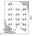
- FIG. 7 shows a top view of ground plane 210 according to an embodiment of the present invention.
- FIG. 8 shows a top view of layer 210 and differential transmission paths 250 ( a )–( e ) according to an embodiment of the present invention.
- FIG. 9 illustrates how the contact section of a signal pad receives a contact element of a connector.
- the present invention provides a multilayered circuit board for use in high-speed data applications.
- FIG. 1 is a top view of a portion of a multilayered circuit board 100 according to an embodiment of the present invention.
- top layer 101 (see FIG. 2 ) of circuit board 100 includes a ground plane 102 , which is made of an electrically conducting material (e.g., copper), and a set of signal pads 104 ( a )–( p ). Because circuit board 100 is intended to be used for transmitting differential signals, each signal pad 104 is paired with another signal pad 104 to form a differential signal pad pair.
- an electrically conducting material e.g., copper
- a first differential signal pad pair is formed by signal pads 104 a and 104 b
- a second pair of signal pads is formed by signal pads 104 c and 104 d
- a third pair of signal pads is formed by signal pads 104 e and 104 f
- a fourth pair of signal pads is formed by signal pads 104 g and 104 h
- a fifth pair of signal pads is formed by signal pads 104 i and 104 j
- a sixth pair of signal pads is formed by signal pads 104 k and 104 l
- a seventh pair of signal pads is formed by signal pads 104 m and 104 n
- an eighth pair of signal pads is formed by signal pads 104 o and 104 p.
- Each signal pad 104 is surrounded by and electrically isolated from the ground plane 102 .
- a clear cut or anti-pad 106 surrounds each signal pad 104 , thereby electrically isolating the signal pad 104 from the surrounding ground plane 102 .
- each signal pad 104 is also electrically isolated from the other signal pads 104 .
- signal pads 104 may be plated with nickel and gold.
- signal pads 104 are elongated (i.e., they have more length than width). In the illustrated embodiments, signal pads 104 may be generally rectangular or generally oval in shape. As shown in FIG. 1 , each signal pad has a hole or “signal via” 108 therein. In some embodiments, the diameter of the signal via is less than about 0.018 or less inches. Each signal via 108 extends through its respective signal pad 104 and through one or more other layers of circuit board 100 . Each signal via 108 is electrically plated and functions to electrically connect its respective signal pad 104 to a transmission line (e.g., a trace) located within circuit board 100 (this is illustrated in FIG. 2 , which is a cross sectional view of circuit board 100 along line 1 — 1 of FIG. 1 ).
- a transmission line e.g., a trace
- circuit board 100 is multilayered.
- the top layer 101 includes ground plane 102 and signal pads 104 .
- the next layer down, layer 202 is a dielectric layer.
- Ground plane 102 and signal pads 104 may be placed onto dielectric layer 202 using conventional techniques.
- Underneath layer 202 is a ground plane 204 (i.e., a layer of electrically conducting material).
- Underneath ground plane 204 is dielectric layer 206 and underneath dielectric layer 206 is dielectric layer 208 .
- a number of differential signal paths 240 ( a )–( c ) are positioned on dielectric layer 208 .
- Each differential signal path 240 includes a first transmission line 241 and a second transmission line 242 .
- Underneath layer 208 is a ground plane 210 .
- Underneath ground plane 210 is dielectric layer 212 and underneath dielectric layer 206 is a dielectric layer 214 .
- a number of differential signal paths 250 ( a )–( e ) are positioned on dielectric layer 214 .
- Each differential signal path 250 includes a first transmission line 251 and a second transmission line 252 .
- Circuit board 100 may have more or less layers than that shown in FIG. 2 .
- signal via 108 ( g ) electrically connects signal pad 104 ( g ) with transmission line 251 ( b ) and signal via 108 ( h ) electrically connects signal pad 104 ( h ) with transmission line 252 ( b ).
- signal via 108 ( i ) electrically connects signal pad 104 ( i ) with transmission line 251 ( d )
- signal via 108 ( j ) electrically connects signal pad 104 ( j ) with transmission line 252 ( d ).
- the signal vias 108 need extend only to a routing layer. The excess via stub can be removed by, e.g., backdrilling. For example, hole 299 was created by backdrilling to shorten the length of signal via 180 ( g ).
- FIG. 3 illustrates a representative signal pad pair (e.g., signal pads 104 a and 104 b ).
- each signal pad 104 has a signal via 108 therein.
- each signal pad 104 has a contact section 310 , the center of which is spaced apart from the center of the signal via 108 .
- the contact section 310 of a signal pad 104 is the portion of the signal pad 104 that receives a contact element 902 (see FIG. 9 ) of a connector 904 . That is, the contact section 310 of a pad 104 is that portion of the pad 104 to which contact element 902 makes physical contact and presses against.
- each signal via 108 is located more towards an end of its respective signal pad 104 than the middle of the pad, as shown in FIG. 3 , to increase the area of the contact section 310 .
- the signal vias 108 are positioned in a signal pad such that the longitudinal axis 390 of the pad bisects or substantially bisects the via 108 .
- the signal pads 104 that make up a signal pad pair are not parallel with respect to each other. Rather, in one embodiment, they form the general shape of a V.
- the signal pads 104 ( a ) and 104 ( b ), which form a signal pad pair are positioned so that the distance between the signal via 108 ( a ), which is positioned at an end of pad 104 ( a ), and the signal via 108 ( b ), which is positioned at an end of signal pad 104 ( b ), is greater than distance between the center of the pad 104 ( a ) and the center of pad 104 ( b ). This is illustrated in FIG.
- D 1 is equal to about 0.080 inches and D 2 is about 0.056 inches.
- W width of a signal pad 104 is about 0.030 inches.
- circuit board 100 has a set of vias 150 that electrically connect ground plane 102 to one or more ground planes within circuit board 100 .
- Vias 150 are referred to as isolvias 150 .
- Isolvias 150 are illustrated in FIG. 4 , which is a cross sectional view of circuit board 100 along line 2 — 2 (see FIG. 1 ). As shown in FIG. 4 , isolvias 150 electrically connect ground plane 102 to ground planes 204 and 210 .
- FIG. 5 shows a top view of ground plane 204 .
- isolvias 150 and signal vias 108 pass through ground plane 204 .
- each signal via 108 is electrically isolated from ground plane 204 by an anti-pad 510 .
- the diameter of each anit-pad 510 is about 0.053 inches.
- FIG. 5 shows how the isolvias 150 and signal vias 108 are arranged in a column and row pattern. For example, as shown in FIG. 5 , signal vias 108 ( a )–( f ) are aligned in a first row; signal vias 108 ( g )–( j ) are aligned in a second row; and signal vias 108 ( k )–( p ) are aligned in a third row. The second row is between the first row and third row. As shown in FIG. 5 , there are four rows of isolvias 150 . Between each row of isolvias 150 there is a row of signal vias 108 .
- the rows of signal vias 108 are arranged such that: signal vias 108 ( a ) and 108 ( k ) are aligned in a first column; signal vias 108 ( b ), 108 ( g ) and 108 ( l ) are aligned in a second column; signal vias 108 ( c ), 108 ( h ), and 108 ( m ) are aligned in a third column; signal vias 108 ( d ), 108 ( i ), and 108 ( n ) are aligned in a fourth column; signal vias 108 ( e ), 108 ( j ), and 108 ( o ) are aligned in a fifth column; and signal vias 108 ( f ) and 108 ( p ) are aligned in a sixth column.
- FIG. 6 shows a top view of layer 208 and differential transmission paths 240 ( a )–( c ).
- Each differential transmission path includes a pair of transmission lines 241 and 242 .
- differential transmission path 240 ( a ) includes transmission line pair 241 ( a ) and 242 ( a ).
- signal vias 108 and isolvias 150 pass through layer 208 .
- some of the signal vias 108 are electrically connected to a transmission line of a differential signal path 240 . More specifically, signal vias 108 ( a ), 108 ( c ), and 108 ( e ) are electrically connected to transmission lines 241 ( a ), ( b ) and ( c ), respectively, and signal vias 108 ( b ), 108 ( d ), and 108 ( f ) are electrically connected to transmission lines 242 ( a ), ( b ) and ( c ), respectively.
- signal vias 108 ( a )–( f ) electrically connect signal contact pads 104 ( a )–( f ) to a transmission line of a differential pair 240 .
- each transmission line 241 , 242 has three sections: a first end section 621 , a second end section 623 , and an interim section 622 between the first end section 621 and the second end 623 .
- the interim section 622 of each transmission line 241 , 242 is straight and they are all parallel with each other. Additionally, the interim sections 622 are substantially longer than the end sections 621 , 623 .
- first end section 621 of a given transmission line 241 , 242 is connected to a first signal via 108 and the second end section 623 of the given transmission line 241 , 242 is connected to a second signal via.
- first end section 621 ( a ) of transmission line 241 ( a ) is physically connected to signal via 108 ( a ) and second end section 623 of transmission line 241 ( a ) is physically connected to signal via 608 ( a ).
- signal via 108 ( a ) is electrically connected to signal via 608 ( a ).
- signal vias 608 like signal vias 108 , are electrically connected to a signal pad 104 .
- neither the first nor second end sections 621 and 623 are aligned with interim section 622 .
- the end sections 621 , 623 are angled with respect to the interim section 622 .
- the end sections 621 , 623 are angled at or about 90 degrees with respect to the interim section (i.e., they are perpendicular to the interim section).
- other angles are contemplated.
- each differential transmission path 240 electrically connects a first pair of signal vias to a second pair of signal vias.
- differential transmission path 240 ( a ) electrically connects a first pair of signal vias (signal vias 108 ( a ) and 108 ( b )) to a second pair of signal signal (vias 608 ( a ) and 608 ( b )).
- transmission line 241 ( a ) electrically connects signal via 108 ( a ) to signal via 608 ( a )
- transmission line 241 ( b ) electrically connects signal via 108 ( b ) to signal via 608 ( b ).
- the distance between the signal vias that make up a pair is greater than the distance between the interim sections of the transmission lines connected to the signal vias.
- This feature is illustrated in FIG. 6 .
- the distance between signal vias 108 ( a ) and 108 ( b ) is greater than the distance between the interim section of transmission line 241 ( a ) and the interim section of transmission line 242 ( a ).
- the distance between signal vias of a pair is generally 0.080 inches and the distance between the interim sections of the transmission lines connected to the vias is generally 0.010 inches.
- the distance between a pair of signal vias connected by a transmission line of a differential path is equal or about equal to the length of the interim section of the transmission line.
- the distance between signal via 108 ( a ) and signal via 608 ( a ) is equal to or about equal to the length of the interim section of transmission line 241 ( a ).
- differential transmission path 240 ( a ) runs between signal via 108 ( k ) and 108 ( l ).
- differential transmission path 240 ( b ) runs between signal via 108 ( m ) and 108 ( n )
- differential transmission path 240 ( c ) runs between signal via 108 ( o ) and 108 ( p ).
- FIG.7 shows a top view of ground plane 210 .
- isolvias 150 and signal vias 108 pass through ground plane 204 .
- each signal via 108 is electrically isolated from ground plane 204 by an anti-pad 710 .
- ground plane 210 is nearly identical to ground plane 204 (see FIG. 5 ).
- the size of anti-pads 710 e.g., the diameter of anit-pad 710 in the case of circular anit-pads
- FIG. 8 shows a top view of layer 214 and differential transmission paths 250 ( a )–( e ).
- Each differential transmission path 250 includes a pair of transmission lines 251 and 252 .
- differential transmission path 250 ( a ) includes transmission line pair 251 ( a ) and 252 ( a ).
- signal vias 108 and isolvias 150 may pass through layer 208 .
- some of the signal vias 108 are electrically connected to a transmission line of a differential signal path 250 . More specifically, signal vias 108 ( k ), 108 ( g ), 108 ( m ), 108 ( i ), and 108 ( o ) are electrically connected to transmission lines 251 ( a )–( d ), respectively, and signal vias 108 ( l ), 108 ( h ), 108 ( n ), 108 ( j ), and 108 ( p ) are electrically connected to transmission lines 252 ( a )–( d ), respectively.
- signal vias 108 ( g )–( p ) electrically connect signal contact pads 104 ( g )–( p ) to a transmission line of a differential pair 250 .
- each transmission line 250 has three sections: a first end section 821 , a second end section 823 , and an interim section 822 connected between the first end section 812 and the second end 823 .
- the interim section 822 of each transmission line 251 , 252 is straight and they are all parallel with each other. Additionally, the interim sections 822 are substantially longer than the end sections 821 , 823 .
- first end section 821 of a given transmission line 251 , 252 is connected to a first signal via 108 and the second end section 823 of the given transmission line 251 , 252 is connected to a second signal via.
- first end section 821 ( a ) of transmission line 251 ( a ) is physically connected to signal via 108 ( k ) and second end section 823 ( a ) of transmission line 251 ( a ) is physically connected to signal via 808 ( a ).
- signal via 108 ( k ) is electrically connected to signal via 608 ( a ).
- signal vias 808 like signal vias 108 , are electrically connected to a signal pad 104 .
- neither the first nor second end sections 821 and 823 are aligned with interim section 822 .
- the end sections 821 , 823 are angled with respect to the interim section 822 .
- the end sections 821 , 823 are angled at or about 90 degrees with respect to the interim section (i.e., they are perpendicular to the interim section).
- other angles are contemplated.
- each differential transmission path 250 electrically connects a first pair of signal vias to a second pair of signal vias.
- differential transmission path 250 ( a ) electrically connects a first pair of signal vias (signal vias 108 ( k ) and 108 ( l )) to a second pair of signal signal (vias 808 ( a ) and 808 ( b )).
- transmission line 251 ( a ) electrically connects signal via 108 ( k ) to signal via 808 ( a )
- transmission line 251 ( b ) electrically connects signal via 108 ( l ) to signal via 808 ( b ).
- the distance between the signal vias that make up a pair is greater than the distance between the interim sections of the transmission lines connected to the signal vias. This feature was discussed above with respect to FIG. 6 and is further illustrated in FIG. 8 . As shown in FIG. 8 , for example, the distance between signal vias 108 ( k ) and 108 ( l ) is greater than the distance between the interim section of transmission line 251 ( a ) and the interim section of transmission line 252 ( b ). As further shown in FIG. 8 , differential transmission path 250 ( b ) runs between signal via 108 ( l ), which is paired with via 108 ( k ), and via 108 ( m ), which is paired with via 108 ( n ). Similarly, differential transmission path 250 ( d ) runs between signal via 108 ( n ), which is paired with via 108 ( m ), and via 108 ( o ), which is paired with via 108 ( p ).
Abstract
Description
Claims (26)
Priority Applications (2)
| Application Number | Priority Date | Filing Date | Title |
|---|---|---|---|
| US10/876,569 US7057115B2 (en) | 2004-01-26 | 2004-06-28 | Multilayered circuit board for high-speed, differential signals |
| PCT/US2005/002436 WO2005074336A2 (en) | 2004-01-26 | 2005-01-26 | Multilayered circuit board for high-speed, differential signals |
Applications Claiming Priority (4)
| Application Number | Priority Date | Filing Date | Title |
|---|---|---|---|
| US53847604P | 2004-01-26 | 2004-01-26 | |
| US53910504P | 2004-01-27 | 2004-01-27 | |
| US53939704P | 2004-01-28 | 2004-01-28 | |
| US10/876,569 US7057115B2 (en) | 2004-01-26 | 2004-06-28 | Multilayered circuit board for high-speed, differential signals |
Publications (2)
| Publication Number | Publication Date |
|---|---|
| US20050161254A1 US20050161254A1 (en) | 2005-07-28 |
| US7057115B2 true US7057115B2 (en) | 2006-06-06 |
Family
ID=34799816
Family Applications (1)
| Application Number | Title | Priority Date | Filing Date |
|---|---|---|---|
| US10/876,569 Expired - Fee Related US7057115B2 (en) | 2004-01-26 | 2004-06-28 | Multilayered circuit board for high-speed, differential signals |
Country Status (2)
| Country | Link |
|---|---|
| US (1) | US7057115B2 (en) |
| WO (1) | WO2005074336A2 (en) |
Cited By (15)
| Publication number | Priority date | Publication date | Assignee | Title |
|---|---|---|---|---|
| US20050265009A1 (en) * | 2004-06-01 | 2005-12-01 | Nokia Corporation | Detecting short circuits and detecting component misplacement |
| US20080093116A1 (en) * | 2006-10-20 | 2008-04-24 | Advanced Semiconductor Engineering, Inc. | Semiconductor substrate for transmitting differential pair |
| US20090049414A1 (en) * | 2007-08-16 | 2009-02-19 | International Business Machines Corporation | Method and system for reducing via stub resonance |
| US7540744B1 (en) | 2008-01-08 | 2009-06-02 | Fci Americas Technology, Inc. | Shared hole orthogonal footprint with backdrilled vias |
| US20090184784A1 (en) * | 2008-01-17 | 2009-07-23 | Sungjun Chun | Reference Plane Voids with Strip Segment for Improving Transmission Line Integrity over Vias |
| US7708569B2 (en) | 2006-10-30 | 2010-05-04 | Fci Americas Technology, Inc. | Broadside-coupled signal pair configurations for electrical connectors |
| US7713088B2 (en) | 2006-10-05 | 2010-05-11 | Fci | Broadside-coupled signal pair configurations for electrical connectors |
| US7837505B2 (en) | 2006-08-21 | 2010-11-23 | Fci Americas Technology Llc | Electrical connector system with jogged contact tails |
| US7837504B2 (en) | 2003-09-26 | 2010-11-23 | Fci Americas Technology, Inc. | Impedance mating interface for electrical connectors |
| US7894204B1 (en) * | 2008-09-02 | 2011-02-22 | The United States Of America As Represented By The Secretary Of The Navy | Matrix board assembly |
| US8444436B1 (en) * | 2004-07-01 | 2013-05-21 | Amphenol Corporation | Midplane especially applicable to an orthogonal architecture electronic system |
| US8542494B2 (en) | 2010-04-29 | 2013-09-24 | International Business Machines Corporation | Circuit board having holes to increase resonant frequency of via stubs |
| US8715003B2 (en) | 2009-12-30 | 2014-05-06 | Fci Americas Technology Llc | Electrical connector having impedance tuning ribs |
| US9136634B2 (en) | 2010-09-03 | 2015-09-15 | Fci Americas Technology Llc | Low-cross-talk electrical connector |
| US20170105284A1 (en) * | 2014-03-24 | 2017-04-13 | Photonics Electronics Technology Research Association | Pad-array structure on substrate for mounting ic chip on substrate, and optical module having said pad-array structure |
Families Citing this family (23)
| Publication number | Priority date | Publication date | Assignee | Title |
|---|---|---|---|---|
| US7108556B2 (en) * | 2004-07-01 | 2006-09-19 | Amphenol Corporation | Midplane especially applicable to an orthogonal architecture electronic system |
| US20060151869A1 (en) * | 2005-01-10 | 2006-07-13 | Franz Gisin | Printed circuit boards and the like with improved signal integrity for differential signal pairs |
| US7081672B1 (en) * | 2005-03-07 | 2006-07-25 | Lsi Logic Corporation | Substrate via layout to improve bias humidity testing reliability |
| TWI278268B (en) * | 2006-02-23 | 2007-04-01 | Via Tech Inc | Arrangement of non-signal through vias and wiring board applying the same |
| US8248816B2 (en) * | 2006-10-31 | 2012-08-21 | Hewlett-Packard Development Company, L.P. | Methods of designing multilayer circuitry, multilayer circuit design apparatuses, and computer-usable media |
| US20100244871A1 (en) * | 2009-02-24 | 2010-09-30 | Qualcomm Incorporated | Space transformer connector printed circuit board assembly |
| US7878860B1 (en) | 2010-04-29 | 2011-02-01 | Winchester Electronics Corporation | Modular connector system |
| WO2011136779A1 (en) * | 2010-04-29 | 2011-11-03 | Winchester Electronics Corporation | Modular connector system |
| US9137887B2 (en) * | 2011-09-07 | 2015-09-15 | Samtec, Inc. | Via structure for transmitting differential signals |
| EP2739125A1 (en) * | 2012-11-28 | 2014-06-04 | Tyco Electronics Svenska Holdings AB | Electrical connection interface for connecting electrical leads for high speed data transmission |
| US9545003B2 (en) * | 2012-12-28 | 2017-01-10 | Fci Americas Technology Llc | Connector footprints in printed circuit board (PCB) |
| US9545004B2 (en) * | 2013-01-29 | 2017-01-10 | Fci Americas Technology Llc | Printed circuit board having orthogonal signal routing |
| US9730313B2 (en) | 2014-11-21 | 2017-08-08 | Amphenol Corporation | Mating backplane for high speed, high density electrical connector |
| US10201074B2 (en) | 2016-03-08 | 2019-02-05 | Amphenol Corporation | Backplane footprint for high speed, high density electrical connectors |
| CN109076700B (en) | 2016-03-08 | 2021-07-30 | 安费诺公司 | Backplane footprints for high speed, high density electrical connectors |
| US10405425B2 (en) * | 2017-06-19 | 2019-09-03 | Dell Products, L.P. | Surface mount technology (SMT) pad design with differential contact strips having converging narrowing distal ends that facilitate high speed communication |
| US10917976B1 (en) * | 2017-07-12 | 2021-02-09 | Juniper Networks, Inc. | Designing a printed circuit board (PCB) to detect slivers of conductive material included within vias of the PCB |
| US10477672B2 (en) * | 2018-01-29 | 2019-11-12 | Hewlett Packard Enterprise Development Lp | Single ended vias with shared voids |
| CN112425274A (en) | 2018-06-11 | 2021-02-26 | 安费诺有限公司 | Backplane footprint for high speed, high density electrical connector |
| TW202019264A (en) | 2018-09-07 | 2020-05-16 | 美商Fci美國有限責任公司 | Connectors for low cost, high speed printed circuit boards |
| EP3973597A4 (en) | 2019-05-20 | 2023-06-28 | Amphenol Corporation | High density, high speed electrical connector |
| CN115298912A (en) | 2020-01-27 | 2022-11-04 | 安费诺有限公司 | Electrical connector with high speed mounting interface |
| CN115315855A (en) | 2020-01-27 | 2022-11-08 | 安费诺有限公司 | Electrical connector with high speed mounting interface |
Citations (23)
| Publication number | Priority date | Publication date | Assignee | Title |
|---|---|---|---|---|
| US4829404A (en) * | 1987-04-27 | 1989-05-09 | Flexmark, Inc. | Method of producing a flexible circuit and master grid therefor |
| US5046966A (en) | 1990-10-05 | 1991-09-10 | International Business Machines Corporation | Coaxial cable connector assembly |
| US5331514A (en) * | 1991-08-05 | 1994-07-19 | Ngk Spark Plug Co., Ltd. | Integrated-circuit package |
| US5557502A (en) | 1995-03-02 | 1996-09-17 | Intel Corporation | Structure of a thermally and electrically enhanced plastic ball grid array package |
| US5726860A (en) * | 1996-03-28 | 1998-03-10 | Intel Corporation | Method and apparatus to reduce cavity size and the bondwire length in three tier PGA packages by interdigitating the VCC/VSS |
| US5784262A (en) * | 1995-11-06 | 1998-07-21 | Symbios, Inc. | Arrangement of pads and through-holes for semiconductor packages |
| US5812378A (en) * | 1994-06-07 | 1998-09-22 | Tessera, Inc. | Microelectronic connector for engaging bump leads |
| US5815374A (en) | 1996-09-30 | 1998-09-29 | International Business Machines Corporation | Method and apparatus for redirecting certain input/output connections of integrated circuit chip configurations |
| US5966293A (en) | 1997-12-15 | 1999-10-12 | Hewlett-Packard Company | Minimal length computer backplane |
| JPH11317471A (en) | 1998-02-19 | 1999-11-16 | Texas Instr Inc <Ti> | Optimal circuit design layout for high performance ball grid array package |
| US6121554A (en) * | 1997-04-30 | 2000-09-19 | Kabushiki Kaisha Toshiba | Printed wiring board |
| US6232564B1 (en) * | 1998-10-09 | 2001-05-15 | International Business Machines Corporation | Printed wiring board wireability enhancement |
| US6235997B1 (en) * | 1997-08-25 | 2001-05-22 | Fujitsu Limited | LSI package with equal length transmission Lines |
| US6384341B1 (en) * | 2001-04-30 | 2002-05-07 | Tyco Electronics Corporation | Differential connector footprint for a multi-layer circuit board |
| US6423909B1 (en) * | 2001-02-27 | 2002-07-23 | Hewlett-Packard Company | Circuit board construction for differential bus distribution |
| US20020185302A1 (en) * | 1998-04-14 | 2002-12-12 | Roy Henson | Method for manufacturing a multi-layer printed circuit board |
| US6528737B1 (en) * | 2000-08-16 | 2003-03-04 | Nortel Networks Limited | Midplane configuration featuring surface contact connectors |
| US6537087B2 (en) * | 1998-11-24 | 2003-03-25 | Teradyne, Inc. | Electrical connector |
| US20030102151A1 (en) * | 1998-09-17 | 2003-06-05 | Naohiro Hirose | Multilayer build-up wiring board |
| EP1330145A2 (en) | 2002-01-18 | 2003-07-23 | Fci | Electrical connection system for two printed circuit boards mounted on opposite sides of a mid-plane printed circuit board at angles to each other |
| US20040188135A1 (en) * | 2003-03-31 | 2004-09-30 | International Business Machines Corporation | Method and structure for implementing enhanced interconnection performance of a land grid array (LGA) module and a printed wiring board |
| US6815621B2 (en) * | 2000-10-02 | 2004-11-09 | Samsung Electronics Co., Ltd. | Chip scale package, printed circuit board, and method of designing a printed circuit board |
| US20050063166A1 (en) * | 2003-09-23 | 2005-03-24 | Intel Corporation | Method and apparatus for providing an integrated printed circuit board registration coupon |
-
2004
- 2004-06-28 US US10/876,569 patent/US7057115B2/en not_active Expired - Fee Related
-
2005
- 2005-01-26 WO PCT/US2005/002436 patent/WO2005074336A2/en active Application Filing
Patent Citations (24)
| Publication number | Priority date | Publication date | Assignee | Title |
|---|---|---|---|---|
| US4829404A (en) * | 1987-04-27 | 1989-05-09 | Flexmark, Inc. | Method of producing a flexible circuit and master grid therefor |
| US5046966A (en) | 1990-10-05 | 1991-09-10 | International Business Machines Corporation | Coaxial cable connector assembly |
| US5331514A (en) * | 1991-08-05 | 1994-07-19 | Ngk Spark Plug Co., Ltd. | Integrated-circuit package |
| US5812378A (en) * | 1994-06-07 | 1998-09-22 | Tessera, Inc. | Microelectronic connector for engaging bump leads |
| US5557502A (en) | 1995-03-02 | 1996-09-17 | Intel Corporation | Structure of a thermally and electrically enhanced plastic ball grid array package |
| US5784262A (en) * | 1995-11-06 | 1998-07-21 | Symbios, Inc. | Arrangement of pads and through-holes for semiconductor packages |
| US5726860A (en) * | 1996-03-28 | 1998-03-10 | Intel Corporation | Method and apparatus to reduce cavity size and the bondwire length in three tier PGA packages by interdigitating the VCC/VSS |
| US5815374A (en) | 1996-09-30 | 1998-09-29 | International Business Machines Corporation | Method and apparatus for redirecting certain input/output connections of integrated circuit chip configurations |
| US6121554A (en) * | 1997-04-30 | 2000-09-19 | Kabushiki Kaisha Toshiba | Printed wiring board |
| US6235997B1 (en) * | 1997-08-25 | 2001-05-22 | Fujitsu Limited | LSI package with equal length transmission Lines |
| US5966293A (en) | 1997-12-15 | 1999-10-12 | Hewlett-Packard Company | Minimal length computer backplane |
| JPH11317471A (en) | 1998-02-19 | 1999-11-16 | Texas Instr Inc <Ti> | Optimal circuit design layout for high performance ball grid array package |
| US20020185302A1 (en) * | 1998-04-14 | 2002-12-12 | Roy Henson | Method for manufacturing a multi-layer printed circuit board |
| US20030102151A1 (en) * | 1998-09-17 | 2003-06-05 | Naohiro Hirose | Multilayer build-up wiring board |
| US6232564B1 (en) * | 1998-10-09 | 2001-05-15 | International Business Machines Corporation | Printed wiring board wireability enhancement |
| US6537087B2 (en) * | 1998-11-24 | 2003-03-25 | Teradyne, Inc. | Electrical connector |
| US6528737B1 (en) * | 2000-08-16 | 2003-03-04 | Nortel Networks Limited | Midplane configuration featuring surface contact connectors |
| US6815621B2 (en) * | 2000-10-02 | 2004-11-09 | Samsung Electronics Co., Ltd. | Chip scale package, printed circuit board, and method of designing a printed circuit board |
| US6423909B1 (en) * | 2001-02-27 | 2002-07-23 | Hewlett-Packard Company | Circuit board construction for differential bus distribution |
| US6384341B1 (en) * | 2001-04-30 | 2002-05-07 | Tyco Electronics Corporation | Differential connector footprint for a multi-layer circuit board |
| US6717825B2 (en) * | 2002-01-18 | 2004-04-06 | Fci Americas Technology, Inc. | Electrical connection system for two printed circuit boards mounted on opposite sides of a mid-plane printed circuit board at angles to each other |
| EP1330145A2 (en) | 2002-01-18 | 2003-07-23 | Fci | Electrical connection system for two printed circuit boards mounted on opposite sides of a mid-plane printed circuit board at angles to each other |
| US20040188135A1 (en) * | 2003-03-31 | 2004-09-30 | International Business Machines Corporation | Method and structure for implementing enhanced interconnection performance of a land grid array (LGA) module and a printed wiring board |
| US20050063166A1 (en) * | 2003-09-23 | 2005-03-24 | Intel Corporation | Method and apparatus for providing an integrated printed circuit board registration coupon |
Non-Patent Citations (1)
| Title |
|---|
| Differential Signals The Differential Difference by Douglas Brooks; a CMP publication, May, 2001; http://www.ultracad.com. * |
Cited By (25)
| Publication number | Priority date | Publication date | Assignee | Title |
|---|---|---|---|---|
| US7837504B2 (en) | 2003-09-26 | 2010-11-23 | Fci Americas Technology, Inc. | Impedance mating interface for electrical connectors |
| US20050265009A1 (en) * | 2004-06-01 | 2005-12-01 | Nokia Corporation | Detecting short circuits and detecting component misplacement |
| US9106020B2 (en) * | 2004-07-01 | 2015-08-11 | Amphenol Corporation | Midplane especially applicable to an orthogonal architecture electronic system |
| US20130337665A1 (en) * | 2004-07-01 | 2013-12-19 | Amphenol Corporation | Midplane Especially Applicable to an Orthogonal Architecture Electronic System |
| US8444436B1 (en) * | 2004-07-01 | 2013-05-21 | Amphenol Corporation | Midplane especially applicable to an orthogonal architecture electronic system |
| US7837505B2 (en) | 2006-08-21 | 2010-11-23 | Fci Americas Technology Llc | Electrical connector system with jogged contact tails |
| US7713088B2 (en) | 2006-10-05 | 2010-05-11 | Fci | Broadside-coupled signal pair configurations for electrical connectors |
| US20080093116A1 (en) * | 2006-10-20 | 2008-04-24 | Advanced Semiconductor Engineering, Inc. | Semiconductor substrate for transmitting differential pair |
| US7708569B2 (en) | 2006-10-30 | 2010-05-04 | Fci Americas Technology, Inc. | Broadside-coupled signal pair configurations for electrical connectors |
| US20090049414A1 (en) * | 2007-08-16 | 2009-02-19 | International Business Machines Corporation | Method and system for reducing via stub resonance |
| US7540744B1 (en) | 2008-01-08 | 2009-06-02 | Fci Americas Technology, Inc. | Shared hole orthogonal footprint with backdrilled vias |
| US8325490B2 (en) * | 2008-01-17 | 2012-12-04 | International Business Machines Corporation | Circuit manufacturing and design techniques for reference plane voids with strip segment |
| US8813000B2 (en) | 2008-01-17 | 2014-08-19 | International Business Machines Corporation | System for designing substrates having reference plane voids with strip segments |
| US7821796B2 (en) * | 2008-01-17 | 2010-10-26 | International Business Machines Corporation | Reference plane voids with strip segment for improving transmission line integrity over vias |
| US20090184784A1 (en) * | 2008-01-17 | 2009-07-23 | Sungjun Chun | Reference Plane Voids with Strip Segment for Improving Transmission Line Integrity over Vias |
| US20100261346A1 (en) * | 2008-01-17 | 2010-10-14 | Sungjun Chun | circuit manufacturing and design techniques for reference plane voids with strip segment |
| US8625300B2 (en) | 2008-01-17 | 2014-01-07 | International Business Machines Corporation | Circuit manufacturing and design techniques for reference plane voids with strip segment |
| US8638567B2 (en) | 2008-01-17 | 2014-01-28 | International Business Machines Corporation | Circuit manufacturing and design techniques for reference plane voids with strip segment |
| US7894204B1 (en) * | 2008-09-02 | 2011-02-22 | The United States Of America As Represented By The Secretary Of The Navy | Matrix board assembly |
| US8715003B2 (en) | 2009-12-30 | 2014-05-06 | Fci Americas Technology Llc | Electrical connector having impedance tuning ribs |
| US8542494B2 (en) | 2010-04-29 | 2013-09-24 | International Business Machines Corporation | Circuit board having holes to increase resonant frequency of via stubs |
| US9119334B2 (en) | 2010-04-29 | 2015-08-25 | Lenovo Enterprise Solutions (Singapore) Pte. Ltd. | Method for manufacturing circuit board having holes to increase resonant frequency of via stubs |
| US9136634B2 (en) | 2010-09-03 | 2015-09-15 | Fci Americas Technology Llc | Low-cross-talk electrical connector |
| US20170105284A1 (en) * | 2014-03-24 | 2017-04-13 | Photonics Electronics Technology Research Association | Pad-array structure on substrate for mounting ic chip on substrate, and optical module having said pad-array structure |
| US9775245B2 (en) * | 2014-03-24 | 2017-09-26 | Photonics Electronics Technology Research Association | Pad-array structure on substrate for mounting IC chip on substrate, and optical module having said pad-array structure |
Also Published As
| Publication number | Publication date |
|---|---|
| US20050161254A1 (en) | 2005-07-28 |
| WO2005074336A2 (en) | 2005-08-11 |
| WO2005074336A3 (en) | 2005-10-06 |
Similar Documents
| Publication | Publication Date | Title |
|---|---|---|
| US7057115B2 (en) | Multilayered circuit board for high-speed, differential signals | |
| US7457132B2 (en) | Via stub termination structures and methods for making same | |
| US8154466B2 (en) | Antenna feed module | |
| KR100904143B1 (en) | Printed circuit board for high-speed electrical connectors | |
| JP4354489B2 (en) | Circuit board and high-speed via system | |
| US8058956B2 (en) | High frequency and wide band impedance matching via | |
| US8120927B2 (en) | Printed circuit board | |
| US8119921B1 (en) | Impedance tuning for circuit board signal path surface pad structures | |
| CA2712949A1 (en) | A radio frequency circuit board topology | |
| TWM400674U (en) | High data rate connector system and circuit board suitable for high frequency signaling | |
| US6054758A (en) | Differential pair geometry for integrated circuit chip packages | |
| US10630002B2 (en) | Circuit board and card | |
| US20180263109A1 (en) | Multi-layer circuit member with reference planes and ground layer surrounding and separating conductive signal pads | |
| US20110036615A1 (en) | Flexible flat circuitry | |
| WO2006060383A2 (en) | Multilayered circuit board for high-speed, differential signals | |
| US9681554B2 (en) | Printed circuit board | |
| EP1714530B1 (en) | Method for increasing a routing density for a circuit board and such a circuit board | |
| CN113161719A (en) | Printed circuit board for base station antenna | |
| US6812576B1 (en) | Fanned out interconnect via structure for electronic package substrates | |
| CN113966647A (en) | Multilayer circuit board | |
| US6888227B2 (en) | Apparatus for routing signals | |
| CN210984936U (en) | Printed circuit board for base station antenna | |
| Ouyang et al. | Methods to reduce crosstalk in flex circuit and PCB | |
| CN218959183U (en) | Printed circuit board and electronic device | |
| US8125087B2 (en) | High-density flip-chip interconnect |
Legal Events
| Date | Code | Title | Description |
|---|---|---|---|
| AS | Assignment |
Owner name: LITTON SYSTEMS, INC., CALIFORNIA Free format text: ASSIGNMENT OF ASSIGNORS INTEREST;ASSIGNORS:CLINK, JAMES;BENHAM, JOHN E.;MITCHELL, JOHN;REEL/FRAME:015526/0216;SIGNING DATES FROM 20040611 TO 20040620 |
|
| AS | Assignment |
Owner name: SOVEREIGN BANK, MASSACHUSETTS Free format text: SECURITY AGREEMENT;ASSIGNORS:WINCHESTER ELECTRONICS CORPORATION;WINCHESTER ELECTRONICS HOLDINGS, LLC;WINCHESTER HOLDING, INC.;REEL/FRAME:017846/0157 Effective date: 20060623 |
|
| AS | Assignment |
Owner name: GLADSTONE CAPITAL CORPORATION, VIRGINIA Free format text: SECURITY AGREEMENT;ASSIGNORS:WINCHESTER ELECTRONICS CORPORATION;WINCHESTER ELECTRONICS HOLDINGS, LLC;WINCHESTER HOLDING, INC.;REEL/FRAME:017858/0850 Effective date: 20060623 |
|
| AS | Assignment |
Owner name: WINCHESTER ELECTRONICS CORPORATION, CONNECTICUT Free format text: ASSIGNMENT OF ASSIGNORS INTEREST;ASSIGNOR:LITTON SYSTEMS, INC.;REEL/FRAME:017906/0555 Effective date: 20060623 |
|
| AS | Assignment |
Owner name: WINCHESTER ELECTRONICS CORPORATION, CONNECTICUT Free format text: RELEASE BY SECURED PARTY;ASSIGNOR:SOVEREIGN BANK;REEL/FRAME:019304/0432 Effective date: 20070504 Owner name: NEWSTAR FINANCIAL, INC., MASSACHUSETTS Free format text: SECURITY AGREEMENT;ASSIGNOR:WINCHESTER ELECTRONICS CORPORATION;REEL/FRAME:019304/0347 Effective date: 20070508 |
|
| FPAY | Fee payment |
Year of fee payment: 4 |
|
| AS | Assignment |
Owner name: MADISON CAPITAL FUNDING LLC, AS AGENT, ILLINOIS Free format text: SECURITY AGREEMENT;ASSIGNOR:WINCHESTER ELECTRONICS CORPORATION;REEL/FRAME:028634/0754 Effective date: 20120725 |
|
| AS | Assignment |
Owner name: WINCHESTER ELECTRONICS CORPORATION, CONNECTICUT Free format text: RELEASE BY SECURED PARTY;ASSIGNOR:GLADSTONE CAPITAL CORPORATION;REEL/FRAME:028725/0026 Effective date: 20120725 Owner name: WINCHESTER HOLDING, INC., CONNECTICUT Free format text: RELEASE BY SECURED PARTY;ASSIGNOR:GLADSTONE CAPITAL CORPORATION;REEL/FRAME:028725/0026 Effective date: 20120725 Owner name: WINCHESTER ELECTRONICS HOLDINGS, LLC, CONNECTICUT Free format text: RELEASE BY SECURED PARTY;ASSIGNOR:GLADSTONE CAPITAL CORPORATION;REEL/FRAME:028725/0026 Effective date: 20120725 Owner name: WINCHESTER ELECTRONICS HOLDINGS, LLC, CONNECTICUT Free format text: RELEASE BY SECURED PARTY;ASSIGNOR:NEWSTAR FINANCIAL, INC.;REEL/FRAME:028725/0038 Effective date: 20120725 Owner name: WINCHESTER HOLDING, INC., CONNECTICUT Free format text: RELEASE BY SECURED PARTY;ASSIGNOR:NEWSTAR FINANCIAL, INC.;REEL/FRAME:028725/0038 Effective date: 20120725 Owner name: WINCHESTER ELECTRONICS CORPORATION, CONNECTICUT Free format text: RELEASE BY SECURED PARTY;ASSIGNOR:NEWSTAR FINANCIAL, INC.;REEL/FRAME:028725/0038 Effective date: 20120725 |
|
| FPAY | Fee payment |
Year of fee payment: 8 |
|
| AS | Assignment |
Owner name: CIT FINANCE LLC, NEW YORK Free format text: SECURITY INTEREST;ASSIGNORS:WINCHESTER ELECTRONICS CORPORATION;CLEMENTS NATIONAL COMPANY;TRU CORPORATION;AND OTHERS;REEL/FRAME:034280/0547 Effective date: 20141117 |
|
| AS | Assignment |
Owner name: WINCHESTER ELECTRONICS CORPORATION, CONNECTICUT Free format text: RELEASE BY SECURED PARTY;ASSIGNOR:MADISON CAPITAL FUNDING LLC;REEL/FRAME:034201/0812 Effective date: 20141117 |
|
| AS | Assignment |
Owner name: WINCHESTER ELECTRONICS CORPORATION, CONNECTICUT Free format text: RELEASE BY SECURED PARTY;ASSIGNOR:MADISON CAPITAL FUNDING LLC;REEL/FRAME:034210/0469 Effective date: 20141117 |
|
| AS | Assignment |
Owner name: WILMINGTON TRUST, NATIONAL ASSOCIATION, AS COLLATE Free format text: SECOND LIEN SECURITY AGREEMENT;ASSIGNORS:WINCHESTER ELECTRONICS CORPORATION;TRU CORPORATION;SRI HERMETICS LLC;AND OTHERS;REEL/FRAME:034306/0792 Effective date: 20141117 |
|
| AS | Assignment |
Owner name: ANTARES CAPITAL LP, AS ADMINISTRATIVE AGENT, ILLIN Free format text: SECURITY INTEREST;ASSIGNORS:CLEMENTS NATIONAL COMPANY;SRI HERMETICS, LLC;TRU CORPORATION;AND OTHERS;REEL/FRAME:039218/0344 Effective date: 20160630 |
|
| AS | Assignment |
Owner name: SRI HERMETICS, LLC, CONNECTICUT Free format text: RELEASE BY SECURED PARTY;ASSIGNOR:WILMINGTON TRUST, NATIONAL ASSOCIATION;REEL/FRAME:039234/0013 Effective date: 20160630 Owner name: WINCHESTER ELECTRONICS CORPORATION, CONNECTICUT Free format text: RELEASE BY SECURED PARTY;ASSIGNOR:WILMINGTON TRUST, NATIONAL ASSOCIATION;REEL/FRAME:039234/0013 Effective date: 20160630 Owner name: TRU CORPORATION, CONNECTICUT Free format text: RELEASE BY SECURED PARTY;ASSIGNOR:WILMINGTON TRUST, NATIONAL ASSOCIATION;REEL/FRAME:039234/0013 Effective date: 20160630 Owner name: CLEMENTS NATIONAL COMPANY, CONNECTICUT Free format text: RELEASE BY SECURED PARTY;ASSIGNOR:WILMINGTON TRUST, NATIONAL ASSOCIATION;REEL/FRAME:039234/0013 Effective date: 20160630 |
|
| AS | Assignment |
Owner name: TRU CORPORATION, CONNECTICUT Free format text: RELEASE BY SECURED PARTY;ASSIGNOR:CIT FINANCE LLC;REEL/FRAME:039379/0882 Effective date: 20160630 Owner name: WINCHESTER ELECTRONICS CORPORATION, CONNECTICUT Free format text: RELEASE BY SECURED PARTY;ASSIGNOR:CIT FINANCE LLC;REEL/FRAME:039379/0882 Effective date: 20160630 Owner name: SRI HERMETICS, LLC, CONNECTICUT Free format text: RELEASE BY SECURED PARTY;ASSIGNOR:CIT FINANCE LLC;REEL/FRAME:039379/0882 Effective date: 20160630 Owner name: CLEMENTS NATIONAL COMPANY, CONNECTICUT Free format text: RELEASE BY SECURED PARTY;ASSIGNOR:CIT FINANCE LLC;REEL/FRAME:039379/0882 Effective date: 20160630 |
|
| FEPP | Fee payment procedure |
Free format text: MAINTENANCE FEE REMINDER MAILED (ORIGINAL EVENT CODE: REM.) |
|
| AS | Assignment |
Owner name: WINCHESTER INTERCONNECT CORPORATION, DELAWARE Free format text: CHANGE OF NAME;ASSIGNOR:WINCHESTER ELECTRONICS CORPORATION;REEL/FRAME:046214/0895 Effective date: 20171130 |
|
| LAPS | Lapse for failure to pay maintenance fees |
Free format text: PATENT EXPIRED FOR FAILURE TO PAY MAINTENANCE FEES (ORIGINAL EVENT CODE: EXP.) |
|
| STCH | Information on status: patent discontinuation |
Free format text: PATENT EXPIRED DUE TO NONPAYMENT OF MAINTENANCE FEES UNDER 37 CFR 1.362 |
|
| FP | Lapsed due to failure to pay maintenance fee |
Effective date: 20180606 |
|
| AS | Assignment |
Owner name: TRU CORPORATION, CONNECTICUT Free format text: RELEASE BY SECURED PARTY;ASSIGNOR:ANTARES CAPITAL LP, AS COLLATERAL AGENT;REEL/FRAME:047878/0322 Effective date: 20181024 Owner name: WINCHESTER ELECTRONICS CORPORATION, CONNECTICUT Free format text: RELEASE BY SECURED PARTY;ASSIGNOR:ANTARES CAPITAL LP, AS COLLATERAL AGENT;REEL/FRAME:047878/0322 Effective date: 20181024 Owner name: CLEMENTS NATIONAL COMPANY, CONNECTICUT Free format text: RELEASE BY SECURED PARTY;ASSIGNOR:ANTARES CAPITAL LP, AS COLLATERAL AGENT;REEL/FRAME:047878/0322 Effective date: 20181024 Owner name: SRI HERMETICS, LLC, CONNECTICUT Free format text: RELEASE BY SECURED PARTY;ASSIGNOR:ANTARES CAPITAL LP, AS COLLATERAL AGENT;REEL/FRAME:047878/0322 Effective date: 20181024 |