US7049661B2 - Semiconductor device having epitaxial layer - Google Patents
Semiconductor device having epitaxial layer Download PDFInfo
- Publication number
- US7049661B2 US7049661B2 US10/699,676 US69967603A US7049661B2 US 7049661 B2 US7049661 B2 US 7049661B2 US 69967603 A US69967603 A US 69967603A US 7049661 B2 US7049661 B2 US 7049661B2
- Authority
- US
- United States
- Prior art keywords
- region
- insulating film
- layer
- soi
- element isolation
- Prior art date
- Legal status (The legal status is an assumption and is not a legal conclusion. Google has not performed a legal analysis and makes no representation as to the accuracy of the status listed.)
- Expired - Fee Related, expires
Links
- 239000004065 semiconductor Substances 0.000 title claims abstract description 62
- 238000002955 isolation Methods 0.000 claims abstract description 95
- 239000000758 substrate Substances 0.000 claims abstract description 59
- 239000000463 material Substances 0.000 claims description 19
- 239000010408 film Substances 0.000 description 177
- 238000000034 method Methods 0.000 description 81
- 235000012431 wafers Nutrition 0.000 description 23
- 238000004519 manufacturing process Methods 0.000 description 21
- VYPSYNLAJGMNEJ-UHFFFAOYSA-N Silicium dioxide Chemical compound O=[Si]=O VYPSYNLAJGMNEJ-UHFFFAOYSA-N 0.000 description 16
- 238000005530 etching Methods 0.000 description 12
- 229910021421 monocrystalline silicon Inorganic materials 0.000 description 10
- XUIMIQQOPSSXEZ-UHFFFAOYSA-N Silicon Chemical compound [Si] XUIMIQQOPSSXEZ-UHFFFAOYSA-N 0.000 description 8
- 229910052681 coesite Inorganic materials 0.000 description 8
- 229910052906 cristobalite Inorganic materials 0.000 description 8
- 229910052710 silicon Inorganic materials 0.000 description 8
- 239000010703 silicon Substances 0.000 description 8
- 239000000377 silicon dioxide Substances 0.000 description 8
- 229910052682 stishovite Inorganic materials 0.000 description 8
- 229910052905 tridymite Inorganic materials 0.000 description 8
- 230000015572 biosynthetic process Effects 0.000 description 7
- 230000000694 effects Effects 0.000 description 7
- 238000001020 plasma etching Methods 0.000 description 6
- 238000001039 wet etching Methods 0.000 description 6
- 238000001312 dry etching Methods 0.000 description 5
- 238000007667 floating Methods 0.000 description 4
- 230000000994 depressogenic effect Effects 0.000 description 3
- 239000012212 insulator Substances 0.000 description 3
- 230000004048 modification Effects 0.000 description 3
- 238000012986 modification Methods 0.000 description 3
- LDDQLRUQCUTJBB-UHFFFAOYSA-N ammonium fluoride Chemical compound [NH4+].[F-] LDDQLRUQCUTJBB-UHFFFAOYSA-N 0.000 description 2
- 230000008901 benefit Effects 0.000 description 2
- 239000013078 crystal Substances 0.000 description 2
- 230000007547 defect Effects 0.000 description 2
- 239000007772 electrode material Substances 0.000 description 2
- 238000005516 engineering process Methods 0.000 description 2
- 230000001965 increasing effect Effects 0.000 description 2
- 150000004767 nitrides Chemical class 0.000 description 2
- 230000003647 oxidation Effects 0.000 description 2
- 238000007254 oxidation reaction Methods 0.000 description 2
- 238000005498 polishing Methods 0.000 description 2
- 229910021420 polycrystalline silicon Inorganic materials 0.000 description 2
- 239000000126 substance Substances 0.000 description 2
- 239000010409 thin film Substances 0.000 description 2
- 229910000577 Silicon-germanium Inorganic materials 0.000 description 1
- QVGXLLKOCUKJST-UHFFFAOYSA-N atomic oxygen Chemical compound [O] QVGXLLKOCUKJST-UHFFFAOYSA-N 0.000 description 1
- 210000000746 body region Anatomy 0.000 description 1
- 230000008878 coupling Effects 0.000 description 1
- 238000010168 coupling process Methods 0.000 description 1
- 238000005859 coupling reaction Methods 0.000 description 1
- 230000003247 decreasing effect Effects 0.000 description 1
- 238000000151 deposition Methods 0.000 description 1
- 230000002708 enhancing effect Effects 0.000 description 1
- 238000002513 implantation Methods 0.000 description 1
- 238000010030 laminating Methods 0.000 description 1
- 229910052760 oxygen Inorganic materials 0.000 description 1
- 239000001301 oxygen Substances 0.000 description 1
- 230000003071 parasitic effect Effects 0.000 description 1
- 238000000206 photolithography Methods 0.000 description 1
- 238000006748 scratching Methods 0.000 description 1
- 230000002393 scratching effect Effects 0.000 description 1
- 238000000926 separation method Methods 0.000 description 1
- 125000006850 spacer group Chemical group 0.000 description 1
Images


Classifications
-
- H—ELECTRICITY
- H01—ELECTRIC ELEMENTS
- H01L—SEMICONDUCTOR DEVICES NOT COVERED BY CLASS H10
- H01L21/00—Processes or apparatus adapted for the manufacture or treatment of semiconductor or solid state devices or of parts thereof
- H01L21/70—Manufacture or treatment of devices consisting of a plurality of solid state components formed in or on a common substrate or of parts thereof; Manufacture of integrated circuit devices or of parts thereof
- H01L21/77—Manufacture or treatment of devices consisting of a plurality of solid state components or integrated circuits formed in, or on, a common substrate
- H01L21/78—Manufacture or treatment of devices consisting of a plurality of solid state components or integrated circuits formed in, or on, a common substrate with subsequent division of the substrate into plural individual devices
- H01L21/82—Manufacture or treatment of devices consisting of a plurality of solid state components or integrated circuits formed in, or on, a common substrate with subsequent division of the substrate into plural individual devices to produce devices, e.g. integrated circuits, each consisting of a plurality of components
- H01L21/822—Manufacture or treatment of devices consisting of a plurality of solid state components or integrated circuits formed in, or on, a common substrate with subsequent division of the substrate into plural individual devices to produce devices, e.g. integrated circuits, each consisting of a plurality of components the substrate being a semiconductor, using silicon technology
- H01L21/8232—Field-effect technology
- H01L21/8234—MIS technology, i.e. integration processes of field effect transistors of the conductor-insulator-semiconductor type
- H01L21/823412—MIS technology, i.e. integration processes of field effect transistors of the conductor-insulator-semiconductor type with a particular manufacturing method of the channel structures, e.g. channel implants, halo or pocket implants, or channel materials
-
- H—ELECTRICITY
- H01—ELECTRIC ELEMENTS
- H01L—SEMICONDUCTOR DEVICES NOT COVERED BY CLASS H10
- H01L21/00—Processes or apparatus adapted for the manufacture or treatment of semiconductor or solid state devices or of parts thereof
- H01L21/70—Manufacture or treatment of devices consisting of a plurality of solid state components formed in or on a common substrate or of parts thereof; Manufacture of integrated circuit devices or of parts thereof
- H01L21/71—Manufacture of specific parts of devices defined in group H01L21/70
- H01L21/76—Making of isolation regions between components
- H01L21/762—Dielectric regions, e.g. EPIC dielectric isolation, LOCOS; Trench refilling techniques, SOI technology, use of channel stoppers
- H01L21/7624—Dielectric regions, e.g. EPIC dielectric isolation, LOCOS; Trench refilling techniques, SOI technology, use of channel stoppers using semiconductor on insulator [SOI] technology
- H01L21/76264—SOI together with lateral isolation, e.g. using local oxidation of silicon, or dielectric or polycristalline material refilled trench or air gap isolation regions, e.g. completely isolated semiconductor islands
-
- H—ELECTRICITY
- H01—ELECTRIC ELEMENTS
- H01L—SEMICONDUCTOR DEVICES NOT COVERED BY CLASS H10
- H01L21/00—Processes or apparatus adapted for the manufacture or treatment of semiconductor or solid state devices or of parts thereof
- H01L21/70—Manufacture or treatment of devices consisting of a plurality of solid state components formed in or on a common substrate or of parts thereof; Manufacture of integrated circuit devices or of parts thereof
- H01L21/77—Manufacture or treatment of devices consisting of a plurality of solid state components or integrated circuits formed in, or on, a common substrate
- H01L21/78—Manufacture or treatment of devices consisting of a plurality of solid state components or integrated circuits formed in, or on, a common substrate with subsequent division of the substrate into plural individual devices
- H01L21/82—Manufacture or treatment of devices consisting of a plurality of solid state components or integrated circuits formed in, or on, a common substrate with subsequent division of the substrate into plural individual devices to produce devices, e.g. integrated circuits, each consisting of a plurality of components
- H01L21/822—Manufacture or treatment of devices consisting of a plurality of solid state components or integrated circuits formed in, or on, a common substrate with subsequent division of the substrate into plural individual devices to produce devices, e.g. integrated circuits, each consisting of a plurality of components the substrate being a semiconductor, using silicon technology
- H01L21/8232—Field-effect technology
- H01L21/8234—MIS technology, i.e. integration processes of field effect transistors of the conductor-insulator-semiconductor type
- H01L21/823437—MIS technology, i.e. integration processes of field effect transistors of the conductor-insulator-semiconductor type with a particular manufacturing method of the gate conductors, e.g. particular materials, shapes
-
- H—ELECTRICITY
- H01—ELECTRIC ELEMENTS
- H01L—SEMICONDUCTOR DEVICES NOT COVERED BY CLASS H10
- H01L21/00—Processes or apparatus adapted for the manufacture or treatment of semiconductor or solid state devices or of parts thereof
- H01L21/70—Manufacture or treatment of devices consisting of a plurality of solid state components formed in or on a common substrate or of parts thereof; Manufacture of integrated circuit devices or of parts thereof
- H01L21/77—Manufacture or treatment of devices consisting of a plurality of solid state components or integrated circuits formed in, or on, a common substrate
- H01L21/78—Manufacture or treatment of devices consisting of a plurality of solid state components or integrated circuits formed in, or on, a common substrate with subsequent division of the substrate into plural individual devices
- H01L21/82—Manufacture or treatment of devices consisting of a plurality of solid state components or integrated circuits formed in, or on, a common substrate with subsequent division of the substrate into plural individual devices to produce devices, e.g. integrated circuits, each consisting of a plurality of components
- H01L21/822—Manufacture or treatment of devices consisting of a plurality of solid state components or integrated circuits formed in, or on, a common substrate with subsequent division of the substrate into plural individual devices to produce devices, e.g. integrated circuits, each consisting of a plurality of components the substrate being a semiconductor, using silicon technology
- H01L21/8232—Field-effect technology
- H01L21/8234—MIS technology, i.e. integration processes of field effect transistors of the conductor-insulator-semiconductor type
- H01L21/823481—MIS technology, i.e. integration processes of field effect transistors of the conductor-insulator-semiconductor type isolation region manufacturing related aspects, e.g. to avoid interaction of isolation region with adjacent structure
-
- H—ELECTRICITY
- H01—ELECTRIC ELEMENTS
- H01L—SEMICONDUCTOR DEVICES NOT COVERED BY CLASS H10
- H01L21/00—Processes or apparatus adapted for the manufacture or treatment of semiconductor or solid state devices or of parts thereof
- H01L21/70—Manufacture or treatment of devices consisting of a plurality of solid state components formed in or on a common substrate or of parts thereof; Manufacture of integrated circuit devices or of parts thereof
- H01L21/77—Manufacture or treatment of devices consisting of a plurality of solid state components or integrated circuits formed in, or on, a common substrate
- H01L21/78—Manufacture or treatment of devices consisting of a plurality of solid state components or integrated circuits formed in, or on, a common substrate with subsequent division of the substrate into plural individual devices
- H01L21/82—Manufacture or treatment of devices consisting of a plurality of solid state components or integrated circuits formed in, or on, a common substrate with subsequent division of the substrate into plural individual devices to produce devices, e.g. integrated circuits, each consisting of a plurality of components
- H01L21/84—Manufacture or treatment of devices consisting of a plurality of solid state components or integrated circuits formed in, or on, a common substrate with subsequent division of the substrate into plural individual devices to produce devices, e.g. integrated circuits, each consisting of a plurality of components the substrate being other than a semiconductor body, e.g. being an insulating body
-
- H—ELECTRICITY
- H01—ELECTRIC ELEMENTS
- H01L—SEMICONDUCTOR DEVICES NOT COVERED BY CLASS H10
- H01L27/00—Devices consisting of a plurality of semiconductor or other solid-state components formed in or on a common substrate
- H01L27/02—Devices consisting of a plurality of semiconductor or other solid-state components formed in or on a common substrate including semiconductor components specially adapted for rectifying, oscillating, amplifying or switching and having at least one potential-jump barrier or surface barrier; including integrated passive circuit elements with at least one potential-jump barrier or surface barrier
- H01L27/04—Devices consisting of a plurality of semiconductor or other solid-state components formed in or on a common substrate including semiconductor components specially adapted for rectifying, oscillating, amplifying or switching and having at least one potential-jump barrier or surface barrier; including integrated passive circuit elements with at least one potential-jump barrier or surface barrier the substrate being a semiconductor body
- H01L27/10—Devices consisting of a plurality of semiconductor or other solid-state components formed in or on a common substrate including semiconductor components specially adapted for rectifying, oscillating, amplifying or switching and having at least one potential-jump barrier or surface barrier; including integrated passive circuit elements with at least one potential-jump barrier or surface barrier the substrate being a semiconductor body including a plurality of individual components in a repetitive configuration
- H01L27/105—Devices consisting of a plurality of semiconductor or other solid-state components formed in or on a common substrate including semiconductor components specially adapted for rectifying, oscillating, amplifying or switching and having at least one potential-jump barrier or surface barrier; including integrated passive circuit elements with at least one potential-jump barrier or surface barrier the substrate being a semiconductor body including a plurality of individual components in a repetitive configuration including field-effect components
-
- H—ELECTRICITY
- H01—ELECTRIC ELEMENTS
- H01L—SEMICONDUCTOR DEVICES NOT COVERED BY CLASS H10
- H01L27/00—Devices consisting of a plurality of semiconductor or other solid-state components formed in or on a common substrate
- H01L27/02—Devices consisting of a plurality of semiconductor or other solid-state components formed in or on a common substrate including semiconductor components specially adapted for rectifying, oscillating, amplifying or switching and having at least one potential-jump barrier or surface barrier; including integrated passive circuit elements with at least one potential-jump barrier or surface barrier
- H01L27/12—Devices consisting of a plurality of semiconductor or other solid-state components formed in or on a common substrate including semiconductor components specially adapted for rectifying, oscillating, amplifying or switching and having at least one potential-jump barrier or surface barrier; including integrated passive circuit elements with at least one potential-jump barrier or surface barrier the substrate being other than a semiconductor body, e.g. an insulating body
- H01L27/1203—Devices consisting of a plurality of semiconductor or other solid-state components formed in or on a common substrate including semiconductor components specially adapted for rectifying, oscillating, amplifying or switching and having at least one potential-jump barrier or surface barrier; including integrated passive circuit elements with at least one potential-jump barrier or surface barrier the substrate being other than a semiconductor body, e.g. an insulating body the substrate comprising an insulating body on a semiconductor body, e.g. SOI
- H01L27/1207—Devices consisting of a plurality of semiconductor or other solid-state components formed in or on a common substrate including semiconductor components specially adapted for rectifying, oscillating, amplifying or switching and having at least one potential-jump barrier or surface barrier; including integrated passive circuit elements with at least one potential-jump barrier or surface barrier the substrate being other than a semiconductor body, e.g. an insulating body the substrate comprising an insulating body on a semiconductor body, e.g. SOI combined with devices in contact with the semiconductor body, i.e. bulk/SOI hybrid circuits
-
- H—ELECTRICITY
- H01—ELECTRIC ELEMENTS
- H01L—SEMICONDUCTOR DEVICES NOT COVERED BY CLASS H10
- H01L29/00—Semiconductor devices adapted for rectifying, amplifying, oscillating or switching, or capacitors or resistors with at least one potential-jump barrier or surface barrier, e.g. PN junction depletion layer or carrier concentration layer; Details of semiconductor bodies or of electrodes thereof ; Multistep manufacturing processes therefor
- H01L29/66—Types of semiconductor device ; Multistep manufacturing processes therefor
- H01L29/68—Types of semiconductor device ; Multistep manufacturing processes therefor controllable by only the electric current supplied, or only the electric potential applied, to an electrode which does not carry the current to be rectified, amplified or switched
- H01L29/76—Unipolar devices, e.g. field effect transistors
- H01L29/772—Field effect transistors
- H01L29/78—Field effect transistors with field effect produced by an insulated gate
- H01L29/7841—Field effect transistors with field effect produced by an insulated gate with floating body, e.g. programmable transistors
-
- H—ELECTRICITY
- H10—SEMICONDUCTOR DEVICES; ELECTRIC SOLID-STATE DEVICES NOT OTHERWISE PROVIDED FOR
- H10B—ELECTRONIC MEMORY DEVICES
- H10B41/00—Electrically erasable-and-programmable ROM [EEPROM] devices comprising floating gates
- H10B41/40—Electrically erasable-and-programmable ROM [EEPROM] devices comprising floating gates characterised by the peripheral circuit region
- H10B41/42—Simultaneous manufacture of periphery and memory cells
- H10B41/43—Simultaneous manufacture of periphery and memory cells comprising only one type of peripheral transistor
-
- H—ELECTRICITY
- H10—SEMICONDUCTOR DEVICES; ELECTRIC SOLID-STATE DEVICES NOT OTHERWISE PROVIDED FOR
- H10B—ELECTRONIC MEMORY DEVICES
- H10B12/00—Dynamic random access memory [DRAM] devices
- H10B12/50—Peripheral circuit region structures
Definitions
- This invention relates to a semiconductor device using a hybrid wafer having an SOI (Silicon On Insulator) region and a bulk region and a manufacturing method thereof.
- SOI Silicon On Insulator
- a method for depositing silicon on a supporting substrate of a bulk region by a selective epitaxial growth method and making the silicon layer flat by polishing as required in order to eliminate the difference in level caused between the SOI region and the bulk region in the third method is provided (refer to “Jpn. Pat. Appln. KOKAI Publication No. 2000-243944” and “T. Yamada, et al., 2002 Symposium on VLSI Technology of Technical Papers, pp. 112–113”).
- the fourth method is excellent in productivity of elements since the difference in level between the element surface of the SOI region and the element surface of the bulk region is eliminated. Further, the fourth method is a method which can flexibly cope with a case wherein the film thickness of the SOI layer or buried insulating film varies or the material of the SOI layer such as a silicon layer or SiGe layer is changed since a semiconductor device is manufactured by use of a ready-made SOI wafer.
- the fourth method has a problem as described below. Before explaining the problem, the fourth method is specifically explained below.
- an SOI wafer having a supporting substrate 111 , buried insulating film 112 and SOI layer 113 is prepared.
- a first mask member (for example, SiN film) 114 is formed on the SOI layer 113 to protect the same.
- the first mask member 114 , SOI layer 113 and buried insulating film 112 in the bulk region are selectively etched and removed in this order.
- a thin buried insulating film 112 ′ is left behind on the supporting substrate 111 .
- a second mask member (for example, SiN film) 116 for protection of the side wall of the SOI layer 113 is formed on the entire surface.
- a spacer formed of the second mask member 116 is formed on the side surface of the SOI layer 113 by an anisotropic dry-etching process.
- a thin buried insulating film 112 ′′ is left behind on the supporting substrate 111 .
- the buried insulating films 112 , 112 ′′ are removed by using an HF solution or the like without giving damage to the supporting substrate 111 .
- the mask members 114 , 116 on the upper portion and side surface of the SOI layer 113 are insulating films of a type different from that of the buried insulating film 112 , the mask members 114 , 116 can be left behind even if the buried insulating films 112 , 112 ′′ are removed.
- an epitaxial layer 117 is formed as an element forming film of single crystal silicon or the like on an exposed portion of the supporting substrate 111 by use of the epitaxial growth technique.
- the epitaxial growth process is performed to adjust the heights of the upper surface of the epitaxial layer 117 and the upper surface of the SOI layer 113 so as to set the upper surface of the epitaxial layer 117 and the upper surface of the SOI layer 113 substantially equal in height to each other.
- a facet 161 is formed on the upper end portion of the epitaxial layer 117 which lies on the SOI region side.
- the first mask member 114 is removed.
- the second mask member 116 formed on the side surface of the SOI layer 113 is removed together with the first mask member 114 since the second mask member 116 is formed of the same material as that of the first mask member 114 .
- a concave portion 160 is formed in the boundary portion between the SOI region and the bulk region.
- gate insulating films 120 , 121 , gate electrodes 122 , 123 , 131 , and element isolation regions 118 , 119 , 130 of the STI (Shallow Trench Isolation) structure are formed.
- the facet 161 and concave portion 160 are formed in the boundary portion between the SOI region and the bulk region. Therefore, in order to eliminate the facet 161 and concave portion 160 , the space for the element isolation region 130 in the boundary portion between the SOI region and the bulk region is made large.
- a semiconductor device comprises a substrate having first to fourth regions, a first insulating film formed on the substrate in the first region, a first epitaxial layer formed on the substrate in the second region and having an upper surface higher than the upper surface of the first insulating film, a first semiconductor layer formed on the first insulating film with a space provided with respect to the first epitaxial layer and having an upper surface set at substantially the same height as the upper surface of the first epitaxial layer, and an element isolation insulating film formed in the space and having an upper surface set at substantially the same height as the upper surface of the first epitaxial layer and the upper surface of the first semiconductor layer.
- a manufacturing method of a semiconductor device comprises forming a wafer including a substrate, a first insulating film formed on the substrate and a semiconductor layer formed on the first insulating film and having first to fourth regions, forming a second insulating film on the semiconductor layer in the first region, removing the first insulating film and the semiconductor layer lying in the second region with the second insulating film used as a mask, forming a space portion in the first region by setting back a side surface of the semiconductor layer on the second region side with respect to a side surface of the first insulating film, forming a first element isolation insulating film in the space portion, forming an epitaxial layer on the substrate in the second region by use of an epitaxial growth process until the upper surface of the epitaxial layer is set substantially equal in height to the upper surface of the semiconductor layer, removing the second insulating film, and forming a first gate electrode on the semiconductor layer in the first region with a first gate insulating film disposed therebetween and forming
- FIG. 1 is a cross sectional view showing a first example of a semiconductor device according to a first embodiment of this invention
- FIGS. 2 to 8 are cross sectional views showing the manufacturing steps of the first example of the semiconductor device according to the first embodiment of this invention.
- FIG. 9 is a cross sectional view showing a second example of the semiconductor device according to the first embodiment of this invention.
- FIGS. 10 to 15 are cross sectional views showing the manufacturing steps of the second example of the semiconductor device according to the first embodiment of this invention.
- FIG. 16 is a cross sectional view showing a third example of the semiconductor device according to the first embodiment of this invention.
- FIGS. 17 , 18 are cross sectional views showing the manufacturing steps of the third example of the semiconductor device according to the first embodiment of this invention.
- FIG. 19 is a cross sectional view showing a fourth example of the semiconductor device according to the first embodiment of this invention.
- FIGS. 20 to 25 are cross sectional views showing the manufacturing steps of the fourth example of the semiconductor device according to the first embodiment of this invention.
- FIG. 26 is a cross sectional view showing another semiconductor device of the fourth example according to the first embodiment of this invention.
- FIG. 27 is a cross sectional view showing a first example of a semiconductor device according to a second embodiment of this invention.
- FIGS. 28 to 32 are cross sectional views showing the manufacturing steps of the first example of the semiconductor device according to the second embodiment of this invention.
- FIG. 33 is a cross sectional view showing a second example of the semiconductor device according to the second embodiment of this invention.
- FIG. 34 is a cross sectional view showing a first example of a semiconductor device according to a third embodiment of this invention.
- FIGS. 35 , 36 are cross sectional views showing the manufacturing steps of the first example of the semiconductor device according to the third embodiment of this invention.
- FIG. 37 is a cross sectional view showing a second example of the semiconductor device according to the third embodiment of this invention.
- FIGS. 38 , 39 are cross sectional views each showing a semiconductor device having a forwardly tapered portion according to each embodiment of this invention.
- FIG. 40 is a cross sectional view showing a semiconductor device having a forwardly tapered portion and facet according to each embodiment of this invention.
- FIGS. 41 to 47 are cross sectional views showing the manufacturing steps of a conventional semiconductor device.
- a semiconductor device uses a hybrid wafer having an SOI (Silicon On Insulator) region and a bulk region.
- SOI Silicon On Insulator
- a space is formed in a boundary portion between the SOI region and the bulk region by setting back the side surface of the SOI layer with respect to the side surface of a buried insulating film in a lateral direction (horizontal direction with respect to the substrate). Then, a mask member used at the time of epitaxial growth is formed in the space and the mask member is left behind as it is and used as an element isolation region.
- the first example of the first embodiment shows the basic structure of the first embodiment in which a space is formed between the SOI layer and the epitaxial layer and a mask member formed in the space and used at the time of epitaxial growth is used as an element isolation region.
- FIG. 1 is a cross sectional view showing a first example of a semiconductor device according to a first embodiment of this invention.
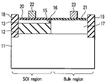
- a buried insulating film 12 is formed on a supporting substrate 11 in the SOI region and an SOI layer 13 is formed on the buried insulating film 12 .
- an epitaxial layer 17 is formed on the supporting substrate 11 and the upper surface of the epitaxial layer 17 is set at substantially the same height as the upper surface of the SOI layer 13 .
- a space portion 15 is formed between the SOI layer 13 and the epitaxial layer 17 since the side surface of the SOI layer 13 which lies on the epitaxial layer 17 side is depressed or set back with respect to the side surface of the buried insulating film 12 which lies on the epitaxial layer 17 side.
- an element isolation region 16 a is formed on the buried insulating film 12 to fill the space portion 15 .
- the upper surface of the element isolation region 16 a is set at substantially the same height as the upper surfaces of the SOI layer 13 and epitaxial layer 17 .
- the SOI layer 13 of the SOI region and the epitaxial layer 17 of the bulk region are electrically isolated from each other by the presence of the element isolation region 16 a .
- the epitaxial layer 17 is formed in contact with the buried insulating film 12 and element isolation region 16 a and is not formed in contact with the SOI layer 13 .
- the element isolation region 16 a by use of the same material (for example, SiO 2 film) as that of the buried insulating film 12 .
- FIGS. 2 to 8 are cross sectional views showing the manufacturing steps of the first example of the semiconductor device according to the first embodiment of this invention. A manufacturing method of the first example according to the first embodiment is explained below.
- an SOI wafer having a supporting substrate 11 , buried insulating film 12 and SOI layer 13 is prepared.
- a p-type silicon substrate having the resistivity of approximately 10 ⁇ cm is used as the supporting substrate 11
- an SiO 2 film having the film thickness of approximately 150 nm is used as the buried insulating film 12
- a single crystal silicon film having the film thickness of approximately 50 nm is used as the SOI layer 13 .
- this is not limitative.
- a first mask member 14 for protection is deposited on the SOI layer 13 .
- the first mask member 14 may be an SiN film or a material film (for example, SiO 2 film) formed of the same material as that of the buried insulating film 12 or a second mask member 16 which will be described later.
- the first mask member 14 , SOI layer 13 and buried insulating film 12 in the bulk region are sequentially etched and removed by a photolithography process or anisotropic dry-etching (for example, RIE (Reactive Ion Etching)) process.
- RIE Reactive Ion Etching
- the SOI layer 13 is removed by an isotropic etching (for example, CDE (Chemical Dry Etching)) process.
- CDE Chemical Dry Etching
- a second mask member (for example, SiO 2 film) 16 for protection of the side wall of the SOI layer 13 is deposited on the entire surface of the structure.
- the film thickness Y of the second mask member 16 is set equal to or larger than half of the film thickness Z of the SOI layer 13 .
- the space portion 15 can be easily filled with the second mask member 16 irrespective of the width X of the space portion 15 corresponding to a distance by which the side surface of the SOI layer 13 is depressed or set back with respect to the side surface of the buried insulating film 12 .
- the second mask member 16 and buried insulating film 12 ′ are etched and removed by an isotropic etching process.
- an isotropic etching process a wet etching process using an HF solution, NH 4 F solution or the like can be used.
- an element isolation region 16 a formed of the second mask member 16 is formed in the space portion 15 and the upper surface of the supporting substrate 11 in the bulk region is exposed.
- an epitaxial layer 17 is formed as an element forming film of single crystal silicon or the like on the exposed portion of the supporting substrate 11 by the epitaxial growth technique.
- the heights of the upper surface of the epitaxial layer 17 and the upper surface of the SOI layer 13 are adjusted so as to be set substantially equal to each other.
- a method for growing an epitaxial layer 17 on the entire surface and then polishing the epitaxial layer 17 to the height of the mask member 14 by use of a CMP (Chemical Mechanical Polish) process to make the surface thereof flat can be used.
- CMP Chemical Mechanical Polish
- a difference in height between the SOI layer 13 and the epitaxial layer 17 by an amount corresponding to the film thickness of the mask member 14 occurs and the flatness and crystallinity of the epitaxial layer 17 may be degraded due to dishing or scratching. Further, it is not preferable from the viewpoint of the cost.
- the first mask member 14 is removed.
- gate insulating films 20 , 21 , gate electrodes 22 , 23 and element isolation regions 18 , 19 of the STI (Shallow Trench Isolation) structure are formed.
- the space portion 15 is formed between the SOI layer 13 and the epitaxial layer 17 by setting back the side surface of the SOI layer 13 with respect to the side surface of the insulating film 12 .
- the mask member 16 for the SOI layer 13 formed in the space portion 15 can be used as the element isolation region 16 a . Therefore, unlike the conventional fourth method, it is not necessary to remove the mask member 116 and the concave portion 160 which occurs when the mask member 116 is removed is not formed. Thus, it is not necessary to form an element isolation region with a large space which is used to remove the concave portion 160 and, as a result, a space for the element isolation region 16 a in the boundary portion between the SOI region and the bulk region can be made small. Further, the depth of the element isolation region 16 a in the boundary portion can be decreased to depth corresponding to the film thickness of the SOI layer 13 .
- a material of the electrode 131 is filled into the concave portion 160 after the concave portion 160 is formed and then the element isolation region 130 is formed to remove the concave portion 160 . Therefore, if an electrode material is filled deep into the concave portion 160 , the electrode material is left behind as a residue in the concave portion 160 in some cases after the element isolation region 130 is processed. As a result, the gate electrodes cross the same boundary portion between the SOI region and the bulk region by plural times and there occurs a possibility that a short-circuiting failure will occur.
- the concave portion 160 is not formed as described above and the problem of occurrence of the short-circuiting failure can be solved.
- the second mask member 116 formed of a material different from that of the buried insulating film 112 is formed on the side surface of the SOI layer 113 so that the side surface of the SOI layer 113 can be prevented from being etched in the step (the step of FIG. 44 ) of removing the buried insulating film 112 ′. Therefore, if the etching condition for removing only the buried insulating film 112 is set, the second mask member 116 is not etched. As a result, only the buried insulating film 112 is etched to a large extent and the side surface of the buried insulating film 112 is set back with respect to the side surface of the second mask member 116 to form an overhang in some cases. If the epitaxial layer 117 is formed while the overhang is formed, a cavity or crystal defect will occur in the overhang portion.
- the element isolation region 16 a can be formed of the same material (for example, SiO 2 film) as that of the buried insulating film 12 . Therefore, in the step (the step of FIG. 6 ) of removing the buried insulating film 12 ′, the buried insulating film 12 and mask member 16 can be removed at the same time while the side surface of the SOI layer 13 is prevented from being etched. Thus, a problem of the overhang as in the conventional case will not occur. As a result, there is no possibility that a cavity or crystal defect will occur due to the overhang in the epitaxial layer 17 .
- a portion for electrically isolating the SOI layer and epitaxial layer and a portion for electrically connecting the SOI layer and epitaxial layer are separately provided in regions between the SOI regions and the bulk regions.
- FIG. 9 is a cross sectional view showing a semiconductor device in a portion for electrically isolating the SOI layer and epitaxial layer and a portion for electrically connecting the SOI layer and epitaxial layer in the second example of the first embodiment.
- a region (which is hereinafter referred to as an insulating region) on the left side of the drawing indicates a portion in which an SOI layer 13 -A and epitaxial layer 17 -A are electrically isolated.
- the insulating region has substantially the same structure as that of the first example of the first embodiment and therefore the explanation thereof is omitted.
- a region (which is hereinafter referred to as a conducting region) on the right side of the drawing indicates a portion in which an SOI layer 13 -B and epitaxial layer 17 -B are electrically connected to each other. That is, the SOI layer 13 -B and epitaxial layer 17 -B are formed in direct contact with each other.
- the other structure is the same as that of the insulating region.
- FIGS. 10 to 15 are cross sectional views showing the manufacturing steps of the second example of the semiconductor device according to the first embodiment of this invention.
- the manufacturing method of the second example according to the first embodiment is explained below. In this case, the explanation for the insulating region having the same structure as that of the first example is simplified.
- a resist 25 is formed to cover the side surface of the SOI layer 13 -B in the conducting region after a thin buried insulating film 12 -B′ is left behind like the first example.
- a space portion 15 is formed in the insulating region. At this time, in the conducting region, no space portion 15 is formed since the side surface of the SOI layer 13 -B is covered with the resist 25 .
- a second mask member (for example, SiO 2 film) 16 is deposited on the entire surface. In the insulating region, the second mask member 16 is formed in the space portion 15 .
- the second mask member 16 and buried insulating films 12 ′-A, 12 ′-B are etched and removed by use of a wet etching process using an HF solution, NH 4 F solution or the like. As a result, the upper surfaces of supporting substrates 11 -A, 11 -B in the bulk region are exposed. In the insulating region, an element isolation region 16 a formed of the second mask member 16 is formed in the space portion 15 .
- epitaxial layers 17 -A, 17 -B are formed as element isolation films of single crystal silicon or the like on the exposed portions of the supporting substrates 11 -A, 11 -B by the epitaxial growth technique.
- the heights of the upper surfaces of the epitaxial layers 17 -A, 17 -B and the upper surfaces of the SOI layers 13 -A, 13 -B are adjusted so as to be set substantially equal to each other.
- the SOI layer 13 -B and epitaxial layer 17 -B are formed in direct contact with each other in the conducting region.
- the SOI layer 13 -A and epitaxial layer 17 -A are not formed in direct contact with each other.
- the first mask members 14 -A, 14 -B are removed.
- gate insulating films 20 -A, 20 -B, 21 -A, 21 -B, gate electrodes 22 -A, 22 -B, 23 -A, 23 -B and element isolation regions 18 -A, 18 -B, 19 -A, 19 -B of the STI structure are formed.
- the same effect as that of the first example of the first embodiment can be attained in the insulating region. Further, in the conducting region, since the SOI layer 13 -B and epitaxial layer 17 -B are formed in direct contact with each other, the structure is effective when it is desired to electrically connect the two layers.
- an element isolation region is newly formed to remove the facet instead of using the mask member in the first example as the element isolation region as it is.
- FIG. 16 is a cross sectional view showing a third example of a semiconductor device according to the first embodiment of this invention.
- the third example of the first embodiment is different from the first example in that an element isolation region 30 which is not a mask member is newly formed to remove the facet of the epitaxial layer 17 .
- the element isolation region 30 is formed to extend from an internal portion of the SOI layer 13 into the epitaxial layer 17 . Further, the element isolation region 30 may be formed to penetrate the buried insulating film 12 and reach an internal portion of the substrate 11 . However, it is only required to electrically isolate the SOI layer 13 and epitaxial layer 17 from each other and it is not always necessary to form the element isolation region 30 which reaches the internal portion of the substrate 11 .
- FIGS. 17 , 18 are cross sectional views showing the manufacturing steps of the third example of the semiconductor device according to the first embodiment of this invention.
- the manufacturing method of the third example according to the first embodiment is explained below. In this case, only a portion which is different from that of the structure of the first example is explained.
- an epitaxial layer 17 is formed as an element forming film of single crystal silicon or the like on an exposed portion of a supporting substrate 11 by the epitaxial growth technique.
- the heights of the upper surface of the epitaxial layer 17 and the upper surface of the SOI layer 13 are adjusted so as to be set substantially equal to each other.
- a facet 26 may be formed on the upper end portion of the epitaxial layer 17 on the SOI region side in some cases.
- an element isolation region 30 of the STI structure is formed to remove the facet after gate insulating films 20 , 21 are formed.
- element isolation regions 18 , 19 in the SOI region and bulk region are formed.
- gate electrodes 22 , 23 , 31 are formed.
- the method is effective when a facet is formed after the epitaxial growth process is performed in the first example.
- the element isolation region 30 of the third example occupies a larger space than the element isolation region 16 a of the first example.
- the element isolation region is not formed to remove the deep concave portion 160 unlike the conventional case, it is of course possible to sufficiently reduce the space of the element isolation region in comparison with the conventional case.
- the element isolation region in the boundary portion between the SOI region and the bulk region is formed only between the SOI layer and the epitaxial layer.
- the element isolation region is formed not only between the SOI layer and the epitaxial layer but also between the buried insulating film and the epitaxial layer.
- FIG. 19 is a cross sectional view showing a fourth example of a semiconductor device according to the first embodiment of this invention.
- the fourth example of the first embodiment is different from the first example in the position of formation of the element isolation region 16 a . That is, the element isolation region 16 a is formed not only between the SOI layer 13 and the epitaxial layer 17 but also between the buried insulating film 12 and the epitaxial layer 17 .
- the side surface of the buried insulating film 12 on the epitaxial layer 17 side is depressed or set back with respect to the side surface of the SOI layer 13 on the epitaxial layer 17 side. Therefore, the width of a space portion 35 between the buried insulating film 12 and the epitaxial layer 17 is larger than the width of a space portion 15 between the SOI layer 13 and the epitaxial layer 17 . In other words, the side surface of the SOI layer 13 on the epitaxial layer 17 side projects from the side surface of the buried insulating film 12 on the epitaxial layer 17 side.
- the contact surface area between the element isolation region 16 a and the epitaxial layer 17 is large, it is preferable to form the element isolation region 16 a by use of an SiN film so as to suppress formation of a facet at the time of epitaxial growth.
- FIGS. 20 to 25 are cross sectional views showing the manufacturing steps of the fourth example of the semiconductor device according to the first embodiment of this invention.
- the manufacturing method of the fourth example according to the first embodiment is explained below. In this case, only a portion having a structure different from that of the first example is explained.
- a first mask member 14 for protection is deposited on an SOI wafer having a supporting substrate 11 , buried insulating film 12 and SOI layer 13 .
- the first mask member 14 may be formed of an SiN film, SiO 2 film or the like, but it is preferably formed of a film of a material different from that of the buried insulating film 12 .
- the first mask member 14 , SOI layer 13 and buried insulating film 12 in the bulk region are sequentially etched and removed by an anisotropic etching (for example, RIE) process.
- anisotropic etching for example, RIE
- a thin buried insulating film 12 ′ may be left behind on the supporting substrate 11 . Then, the side surface of the SOI layer 13 is set back with respect to the side surface of the buried insulating film 12 to form a space portion 15 .
- the buried insulating film 12 is etched by the isotropic etching process to set back the side surface of the buried insulating film 12 with respect to the side surface of the first mask member 14 so as to form a space portion 35 .
- a second mask member (for example, SiN film) 16 for protection of the side wall of the SOI layer 13 is deposited on the entire surface of the structure.
- the second mask member 16 and buried insulating film 12 ′ are etched and removed by an isotropic etching process.
- an element isolation region 16 a formed of the second mask member 16 is formed in the space portions 15 , 35 and the upper surface of the supporting substrate 11 in the bulk region is exposed.
- an epitaxial layer 17 is formed as an element forming film of single crystal silicon or the like on the exposed portion of the supporting substrate 11 by the epitaxial growth technique.
- the heights of the upper surface of the epitaxial layer 17 and the upper surface of the SOI layer 13 are adjusted so as to be set substantially equal to each other.
- the first mask member 14 is removed after the epitaxial growth process.
- gate insulating films 20 , 21 , gate electrodes 22 , 23 , 31 and element isolation regions 18 , 19 of the STI structure are formed.
- the mask member 16 for the SOI layer 13 formed at the time of epitaxial growth can be used as the element isolation region 16 a as it is. Therefore, a space of the element isolation region can be reduced.
- the element isolation region 16 a of the fourth example occupies a larger space than the element isolation region 16 a of the first example.
- the element isolation region is not formed to remove the deep concave portion 160 , and therefore, it is of course possible to sufficiently reduce the space (particularly, the lateral width of the element isolation region) of the element isolation region in comparison with the conventional case.
- the element isolation region 16 a is formed of an SiN film which is different from a material of the buried insulating film 12 . It is known that, in the selective epitaxial growth process, a facet can be made smaller (or formation of a facet can be prevented) on the epitaxial layer 17 when a boundary surface is formed between the epitaxial process 17 and the SiN film than when a boundary surface is formed between the epitaxial process 17 and the SiO 2 film. Therefore, formation of the facet on the boundary between the element isolation region 16 a and the epitaxial process 17 can be suppressed by forming the element isolation region 16 a by use of the SiN film.
- the side surface of the buried insulating film 12 is set back with respect to the side surface of the SOI layer 13 is shown.
- the side surface of the SOI layer 13 can be set back with respect to the side surface of the buried insulating film 12 . Therefore, the width of the space portion 15 can be made smaller than that of the space portion 35 ( FIG. 19 ) or the width of the space portion 35 can be made smaller than that of the space portion 15 ( FIG. 26 ).
- the second embodiment is an example in which the epitaxial growth process is not performed and an attempt is made to reduce a apace of an element isolation region in a boundary portion between an SOI region and a bulk region.
- the first example of the second embodiment is to form gate electrodes of a two-layered structure in the SOI region and bulk region and set the heights of the upper surfaces of both of the gate electrodes substantially equal to each other although the heights of the undersurfaces of both of the gate electrodes are different.
- FIG. 27 is a cross sectional view showing the first example of a semiconductor device according to the second embodiment of this invention.
- a gate insulating film 20 is formed on an SOI layer 13 and a gate electrode 45 is formed on the gate insulating film 20 .
- the gate electrode 45 has a two-layered structure having a lower electrode layer 43 a and an upper electrode layer 44 a.
- a gate insulating film 21 is formed on a supporting substrate 11 and a gate electrode 46 is formed on the gate insulating film 21 .
- the gate electrode 46 has a two-layered structure having a lower electrode layer 43 b and an upper electrode layer 44 b.
- the gate electrode 45 in the SOI region and the gate electrode 46 in the bulk region are different in the height of the substrate portions under the gate electrodes, but are substantially equal in the height of the upper surfaces of the gate electrodes. That is, the electrode layer 43 b of the gate electrode 46 of the bulk region is made thicker than the electrode layer 43 a of the gate electrode 45 of the SOI region so as to eliminate a difference in the height of the substrate portions under the gate electrodes of the SOI region and bulk region.
- an element isolation region 41 of the STI structure is formed in a boundary portion between the SOI region and the bulk region.
- the SOI layer 13 is electrically isolated from the substrate 11 of the bulk region.
- element isolation regions 40 , 42 are respectively formed in the SOI region and bulk region. It is preferable to form the element isolation region 41 by use of a material different from that of the buried insulating film 12 .
- FIGS. 28 to 32 are cross sectional views showing the manufacturing steps of the first example of the semiconductor device according to the second embodiment of this invention. The manufacturing method of the first example of the second embodiment is explained below.
- an SOI wafer having a supporting substrate 11 , buried insulating film 12 and SOI layer 13 is prepared.
- element isolation regions 40 , 41 , 42 are formed to extend from the surface of the SOI layer 13 into the supporting substrate 11 .
- the upper portions of the element isolation regions 40 , 41 , 42 are formed to project from the upper surface of the SOI layer 13 so as to form concave portions 48 .
- the SOI layer 13 and buried insulating film 12 in the bulk region are removed.
- the concave portion 48 is kept unchanged and a concave portion 49 which is deeper than the concave portion 48 is formed in the bulk region.
- a gate insulating film 20 is formed on the SOI layer 13 and a gate insulating film 20 is formed on the supporting substrate 11 . Then, a first electrode member 43 is formed on the gate insulating films 20 , 21 and element isolation regions 40 , 41 , 42 .
- the upper surface of the first electrode member 43 is polished and made flat by the CMP process until the upper surfaces of the element isolation regions 40 , 41 , 42 are exposed. Therefore, the lower electrode layer 43 a of the gate electrode in the SOI region is formed in the concave portion 48 and the lower electrode layer 43 b of the gate electrode in the bulk region is formed in the concave portion 49 .
- the upper surface of the lower electrode layer 43 a in the SOI region and the upper surface of the lower electrode layer 43 b in the bulk region can be set equal in height to each other and a difference in level between the SOI region and the bulk region can be eliminated.
- a second electrode member 44 is formed on the lower electrode layers 43 a , 43 b and element isolation regions 40 , 41 , 42 .
- the lower electrode layers 43 a , 43 b and second electrode member 44 are simultaneously processed.
- a gate electrode 45 formed of the lower electrode layer 43 a and upper electrode layer 44 a is formed in the SOI region and a gate electrode 46 formed of the lower electrode layer 43 b and upper electrode layer 44 b is formed in the bulk region.
- the selective epitaxial growth process is not performed in the bulk region, a difference in level occurs between the SOI region and the bulk region.
- the difference in level can be eliminated by use of the lower electrode layers 43 a , 43 b of the gate electrodes. Therefore, the gate electrodes 45 , 46 of the same height can be formed in the SOI region and bulk region.
- the second example of the second embodiment is a modification of the first example and is an example in which an EEPROM is formed in the bulk region.
- FIG. 33 is a cross sectional view showing the second example of a semiconductor device according to the second embodiment of this invention. In this case, the structure which is different from that of the first example is mainly explained.
- an insulating film 47 such as an ONO (Oxide Nitride Oxide) film is formed between the upper electrode layer 44 b and the lower electrode layer 43 b in the bulk region. That is, an EEPROM cell having the lower electrode layer 43 b used as a floating gate and the upper electrode layer 44 b used as a control gate is formed in the bulk region.
- ONO Oxide Nitride Oxide
- the structure which eliminates the difference in level between the SOI region and the bulk region is different from that of the first example. That is, the lower electrode layer 43 b is formed with substantially the same thickness as the lower electrode layer 43 a and the difference in level between the SOI region and the bulk region is eliminated by use of the upper electrode layer 44 b and insulating film 47 .
- the lower electrode layer 43 b has side surface portions formed along the side surfaces (the side surfaces of the element isolation regions 41 , 42 ) of the concave portion 49 and a bottom surface portion formed along the bottom surface (on the gate insulating film 21 ) of the concave portion 49 .
- the insulating film 47 has side surface portions formed along the side surface portions of the lower electrode layer 43 b , a bottom surface portion formed along the bottom surface portion of the lower electrode layer 43 b and upper portions formed along the upper surfaces of the element isolation regions 41 , 42 and lower electrode layer 43 b . That is, the lower electrode layer 43 b and insulating film 47 in the bulk region have a concave structure formed according to the shape of the concave portion 49 . Further, since the upper electrode layer 44 b is formed to fill the concave portion of the concave structure formed of the lower electrode layer 43 b and insulating film 47 , the central portion of the upper electrode layer 44 b is made thicker than the end portion thereof.
- the lower electrode layer 43 b and insulating film 47 in the bulk region are formed in a concave shape by use of the difference in level between the SOI region and the bulk region. Therefore, an adequate coupling ratio between the upper electrode layer 44 b and the lower electrode layer 43 b can be attained and thus a merit that the operation of the cell can be stabilized can be obtained.
- the third embodiment is an example in which a buried insulating film and SOI layer in an SOI region are used as a gate insulating film and gate electrode in a bulk region.
- the first example of the third embodiment shows a basic structure in which a buried insulating film and SOI layer in an SOI region are used as a gate insulating film and gate electrode in a bulk region.
- FIG. 34 is a cross sectional view showing the first example of a semiconductor device according to the third embodiment of this invention.
- a buried insulating film 12 a in the SOI region is formed relatively thin and an insulating film used as the buried insulating film 12 a is also used as a gate insulating film 12 b in the bulk region.
- a layer used as an SOI layer 13 a in the SOI region is also used as a lower electrode layer 13 b of a gate electrode 54 in the bulk region.
- an electrode layer used as a gate electrode in the SOI region is also used as an upper electrode layer 53 b of the gate electrode 54 in the bulk region.
- the heights of the substrate portions which lie under the gate electrode 53 a in the SOI region and the gate electrode 54 in the bulk region are different.
- the heights of the upper surfaces of the gate electrodes 53 a , 54 are set substantially equal to each other. That is, the difference in level between the substrate portions lying under the gate electrodes in the SOI region and the bulk region can be eliminated by forming the gate electrode 54 in the bulk region with a two-layered structure.
- the SOI layer 13 a is formed of a single crystal silicon layer, for example, a layer (lower electrode layer 13 b ) which is part of the gate electrode 54 in the bulk region is formed of a single crystal silicon layer.
- FIGS. 35 , 36 are cross sectional views showing the manufacturing steps of the first example of the semiconductor device according to the third embodiment of this invention. The manufacturing method of the first example of the third embodiment is explained below.
- an SOI wafer having a supporting substrate 11 , buried insulating film 12 and SOI layer 13 is prepared. Then, element isolation regions 50 , 51 , 52 are formed to extend from the surface of the SOI layer 13 into the supporting substrate 11 . As a result, a buried insulating film 12 a and SOI layer 13 a are formed in the SOI region. In the bulk region, a gate insulating film 12 b formed of the buried insulating film 12 is formed and a lower electrode layer 13 b for the gate electrode which is formed of the SOI layer 13 is formed.
- a gate insulating film 20 is formed on the SOI layer 13 a in the SOI region. After this, an electrode member 53 is formed on the entire surface.
- the electrode member 53 and lower electrode layer 13 b are simultaneously processed.
- a gate electrode 53 a formed of the electrode member 53 is formed in the SOI region.
- a gate electrode 54 of the two-layered structure having the lower electrode layer 13 b and an upper electrode layer 53 b formed of the electrode member 53 is formed in the bulk region.
- the selective epitaxial growth process is not performed in the bulk region, a difference in level occurs between the SOI region and the bulk region.
- the difference in level can be eliminated by forming the gate electrode 54 in the bulk region in a two-layered structure form. Therefore, the gate electrodes 53 a , 54 of the same height can be formed in the SOI region and bulk region.
- the material layer used to form the buried insulating film 12 a , SOI layer 13 a and gate electrode 53 a in the SOI region is also used as the material layer to form the gate insulating film 12 b and the lower electrode layer 13 b and upper electrode layer 53 b of the gate electrode 54 in the bulk region. Therefore, the process can be simplified since it is not necessary to additionally provide a new step when elements in the bulk region are formed.
- the buried insulating film 12 a in the SOI region is used as the gate insulating film 12 b in the bulk region and the SOI layer 13 a in the SOI region is used as the gate electrode (lower electrode layer 13 b ) in the bulk region.
- the SOI layer 13 in this embodiment is formed of single crystal silicon, grains occurring when the layer is formed of polycrystalline silicon are not formed. Therefore, a problem associated with the grains can be solved in the present embodiment. For example, it becomes possible to form a gate insulating film with uniform film thickness, prevent a lowering in the withstand voltage from the microscopic viewpoint and further reduce the film thickness. Further, the gate electrode of single crystal silicon has lower wiring resistance than the gate electrode of polycrystalline silicon.
- the second example of the third embodiment is attained by adding an EEPROM in the bulk region of the first example.
- FIG. 37 is a cross sectional view showing the second example of a semiconductor device according to the third embodiment of this invention.
- a gate electrode layer 53 a with the single-layered structure is formed in the SOI region and a gate electrode 54 with the two-layered structure and a gate electrode 56 of the EEPROM are formed in the bulk region.
- a gate insulating film 12 c is formed of the same film 12 as buried insulating films 12 a , 12 b .
- a lower electrode layer 13 c functioning as a floating gate is formed of the same layer 13 as an SOI layer 13 a and lower electrode layer 13 b and an insulating film 20 b is formed of the same film 20 as a gate insulating film 20 a .
- an upper electrode layer 53 c functioning as a control gate is formed of the same layer 53 as a gate electrode 53 a and upper electrode layer 53 b.
- the heights of the substrate portions which lie under the gate electrode 53 a in the SOI region and the gate electrodes 54 , 56 in the bulk region are different.
- the heights of the upper surfaces of the gate electrodes 53 a , 54 , 56 are set substantially equal to each other. That is, the difference in level between the substrate portions lying under the gate electrodes in the SOI region and the bulk region can be eliminated by forming the gate electrodes 54 , 56 with a two-layered structure in the bulk region.
- the gate insulating film 12 c , lower gate electrode 13 c , insulating film 20 b and upper electrode layer 53 c are respectively formed by use of the same layers as the buried insulating film 12 a , SOI layer 13 a , gate insulating film 20 a and gate electrode 53 a . Therefore, the process can be simplified since it is not necessary to additionally provide a new step of forming an EEPROM in the bulk region.
- the final removing method for the buried insulating film 12 in the bulk region is not limited to the wet etching process.
- regions having different setback amounts are formed by use of a resist process and the insulating region and conducting region explained in the second example of the first embodiment can be separately formed only according to the degree of setback amounts.
- the space portion 15 can be formed as follows. First, as shown in FIG. 38 , a first mask member 14 is patterned by use of the RIE process. Then, the SOI layer 13 is removed by use of the isotropic etching process to form a space portion 15 . At this time, as the isotropic etching process, for example, a dry etching process by CDE, a wet etching process by use of a KOH solution or the like is used. Therefore, in this case, since a forwardly tapered surface 62 is formed on the side surface of the SOI layer 13 , a possibility that a problem caused by a film residue occurs in film formation can be further suppressed.
- the isotropic etching process for example, a dry etching process by CDE, a wet etching process by use of a KOH solution or the like is used. Therefore, in this case, since a forwardly tapered surface 62 is formed on the side surface of the SOI layer 13 , a possibility that a problem
- the space portion 15 is formed, the buried insulating film 12 in the bulk region is etched by the RIE process and wet etching process. After this, a process in which no material is filled into the space portion 15 is performed and a structure as shown in FIG. 39 or 40 is completed.
- FIG. 39 shows a structure when no facet is formed on the epitaxial layer 17 and
- FIG. 40 shows a structure when a facet 26 is formed on the epitaxial layer 17 .
- the element isolation region 16 a is formed after the SOI layer 13 and buried insulating film 12 in the bulk region are removed, but this is not limitative. For example, it is possible to remove the SOI layer 13 and buried insulating film 12 in the bulk region after the element isolation region 16 a is formed at least in the boundary portion between the SOI region and the bulk region. After this, an epitaxial growth process may be performed.
- Various materials and crystallinities applied to formation of a device can be applied as the materials and crystallinities of the SOI layer 13 , buried insulating film 12 , supporting substrate 11 , mask members 14 , 16 and epitaxial layer 17 .
- the upper surface of the element isolation region 16 a is set at substantially the same height as the upper surfaces of the SOI layer 13 and epitaxial layer 17 , but this is not limitative. However, the upper surface of the element isolation region 16 a can be set somewhat higher or lower than the upper surfaces of the SOI layer 13 and epitaxial layer 17 . For example, if the element isolation region 16 a is formed of an oxide film, the upper surface of the element isolation region 16 a can be set somewhat lower than the upper surfaces of the SOI layer 13 and epitaxial layer 17 by the oxide film removing process.
- the element isolation region 16 a is formed of a nitride film, the height of the upper surface of the element isolation region 16 a is kept unchanged by the oxidation process or oxide film removing process. However, in this case, the upper surfaces of the SOI layer 13 and epitaxial layer 17 may be lowered by the oxidation process or oxide film removing process. As a result, the upper surface of the element isolation region 16 a can be set higher than the upper surfaces of the SOI layer 13 and epitaxial layer 17 .
Abstract
A semiconductor device includes a substrate having first to fourth regions, a first insulating film formed on the substrate in the first region, a first epitaxial layer formed on the substrate in the second region and having an upper surface higher than an upper surface of the first insulating film, a first semiconductor layer formed on the first insulating film with a space provided with respect to the first epitaxial layer and having an upper surface set at substantially the same height as the upper surface of the first epitaxial layer, and an element isolation insulating film formed in the space and having an upper surface set at substantially the same height as the upper surface of the first epitaxial layer and the upper surface of the first semiconductor layer.
Description
This application is based upon and claims the benefit of priority from the prior Japanese Patent Application No. 2003-209311, filed Aug. 28, 2003, the entire contents of which are incorporated herein by reference.
1. Field of the Invention
This invention relates to a semiconductor device using a hybrid wafer having an SOI (Silicon On Insulator) region and a bulk region and a manufacturing method thereof.
2. Description of the Related Art
Recently, various attempts for lowering the parasitic capacitance, lowering the power consumption of a logic circuit and enhancing the operation speed of the logic circuit have been made by using a thin film SOI (Silicon On Insulator) wafer instead of the conventional silicon wafer and forming elements on the SOI wafer. Further, microprocessors using the SOI wafers have been commercialized. In the future, it is predicted that the necessity for a system LSI using the above SOI logic as a core is increased.
However, since the potential of a body region in which the channel of a MOSFET on the SOI wafer is formed is set into an electrically floating state, a variation in the threshold voltage occurs and a leakage current caused by the circuit operation occurs due to the so-called floating body effect. Therefore, it is not suitable to apply the SOI wafer to a circuit such as cell transistors of a DRAM or paired transistors of a sense amplifier circuit or analog circuit which has a severe specification for a leakage current level or matching characteristic.
In order to solve the above problem, it is proposed to prepare a hybrid wafer having a bulk region formed on the SOI wafer and form a circuit such as a DRAM which is not suitable for the SOI wafer on the bulk region. More specifically, the following methods are provided, for example.
First, a method for selectively forming an SOI region on the bulk wafer by use of an SIMOX (Separation by Implantation of Oxygen) using a mask pattern is provided (refer to “Jpn. Pat. Appln. KOKAI Publication No. 10-303385” and “Robert Hannon, et al., 2000 Symposium on VLSI Technology of Technical Papers, pp. 66–67”).
Second, a method for laminating a wafer on a bulk wafer having a patterned insulating film thereon is provided (refer to Jpn. Pat. Appln. KOKAI Publication No. 8-316431).
Third, a method for selectively and partially etching and removing an SOI layer on the SOI wafer and a buried insulating film formed therein is provided (refer to Jpn. Pat. Appln. KOKAI Publication No. 7-106434, Jpn. Pat. Appln. KOKAI Publication No. 11-238860, and Jpn. Pat. Appln. KOKAI Publication No. 2000-91534).
Fourth, a method for depositing silicon on a supporting substrate of a bulk region by a selective epitaxial growth method and making the silicon layer flat by polishing as required in order to eliminate the difference in level caused between the SOI region and the bulk region in the third method is provided (refer to “Jpn. Pat. Appln. KOKAI Publication No. 2000-243944” and “T. Yamada, et al., 2002 Symposium on VLSI Technology of Technical Papers, pp. 112–113”).
In the above various methods using the hybrid wafer, the fourth method is excellent in productivity of elements since the difference in level between the element surface of the SOI region and the element surface of the bulk region is eliminated. Further, the fourth method is a method which can flexibly cope with a case wherein the film thickness of the SOI layer or buried insulating film varies or the material of the SOI layer such as a silicon layer or SiGe layer is changed since a semiconductor device is manufactured by use of a ready-made SOI wafer.
However, the fourth method has a problem as described below. Before explaining the problem, the fourth method is specifically explained below.
First, as shown in FIG. 41 , an SOI wafer having a supporting substrate 111, buried insulating film 112 and SOI layer 113 is prepared.
Then, as shown in FIG. 42 , a first mask member (for example, SiN film) 114 is formed on the SOI layer 113 to protect the same. Next, the first mask member 114, SOI layer 113 and buried insulating film 112 in the bulk region are selectively etched and removed in this order. At this time, a thin buried insulating film 112′ is left behind on the supporting substrate 111.
After this, as shown in FIG. 43 , a second mask member (for example, SiN film) 116 for protection of the side wall of the SOI layer 113 is formed on the entire surface. Then, a spacer formed of the second mask member 116 is formed on the side surface of the SOI layer 113 by an anisotropic dry-etching process. At this time, as in the step shown in FIG. 42 , a thin buried insulating film 112″ is left behind on the supporting substrate 111.
Next, as shown in FIG. 44 , the buried insulating films 112, 112″ are removed by using an HF solution or the like without giving damage to the supporting substrate 111. In this case, since the mask members 114, 116 on the upper portion and side surface of the SOI layer 113 are insulating films of a type different from that of the buried insulating film 112, the mask members 114, 116 can be left behind even if the buried insulating films 112, 112″ are removed.
Then, as shown in FIG. 45 , an epitaxial layer 117 is formed as an element forming film of single crystal silicon or the like on an exposed portion of the supporting substrate 111 by use of the epitaxial growth technique. The epitaxial growth process is performed to adjust the heights of the upper surface of the epitaxial layer 117 and the upper surface of the SOI layer 113 so as to set the upper surface of the epitaxial layer 117 and the upper surface of the SOI layer 113 substantially equal in height to each other. In this case, a facet 161 is formed on the upper end portion of the epitaxial layer 117 which lies on the SOI region side.
Next, as shown in FIG. 46 , the first mask member 114 is removed. At this time, the second mask member 116 formed on the side surface of the SOI layer 113 is removed together with the first mask member 114 since the second mask member 116 is formed of the same material as that of the first mask member 114. As a result, a concave portion 160 is formed in the boundary portion between the SOI region and the bulk region.
Then, as shown in FIG. 47 , gate insulating films 120, 121, gate electrodes 122, 123, 131, and element isolation regions 118, 119, 130 of the STI (Shallow Trench Isolation) structure are formed.
With the fourth method of the prior art, the facet 161 and concave portion 160 are formed in the boundary portion between the SOI region and the bulk region. Therefore, in order to eliminate the facet 161 and concave portion 160, the space for the element isolation region 130 in the boundary portion between the SOI region and the bulk region is made large.
A semiconductor device according to a first aspect of the invention comprises a substrate having first to fourth regions, a first insulating film formed on the substrate in the first region, a first epitaxial layer formed on the substrate in the second region and having an upper surface higher than the upper surface of the first insulating film, a first semiconductor layer formed on the first insulating film with a space provided with respect to the first epitaxial layer and having an upper surface set at substantially the same height as the upper surface of the first epitaxial layer, and an element isolation insulating film formed in the space and having an upper surface set at substantially the same height as the upper surface of the first epitaxial layer and the upper surface of the first semiconductor layer.
A manufacturing method of a semiconductor device according to a second aspect of the invention comprises forming a wafer including a substrate, a first insulating film formed on the substrate and a semiconductor layer formed on the first insulating film and having first to fourth regions, forming a second insulating film on the semiconductor layer in the first region, removing the first insulating film and the semiconductor layer lying in the second region with the second insulating film used as a mask, forming a space portion in the first region by setting back a side surface of the semiconductor layer on the second region side with respect to a side surface of the first insulating film, forming a first element isolation insulating film in the space portion, forming an epitaxial layer on the substrate in the second region by use of an epitaxial growth process until the upper surface of the epitaxial layer is set substantially equal in height to the upper surface of the semiconductor layer, removing the second insulating film, and forming a first gate electrode on the semiconductor layer in the first region with a first gate insulating film disposed therebetween and forming a second gate electrode on the epitaxial layer in the second region with a second gate insulating film disposed therebetween.
A semiconductor device according to embodiments of this invention uses a hybrid wafer having an SOI (Silicon On Insulator) region and a bulk region. There will now be described embodiments of this invention with reference to the accompanying drawings. In explaining the invention, the same reference symbols are attached to common portions throughout the drawings.
In the first embodiment, a space is formed in a boundary portion between the SOI region and the bulk region by setting back the side surface of the SOI layer with respect to the side surface of a buried insulating film in a lateral direction (horizontal direction with respect to the substrate). Then, a mask member used at the time of epitaxial growth is formed in the space and the mask member is left behind as it is and used as an element isolation region.
Next, first to fourth examples of the first embodiment are explained below.
The first example of the first embodiment shows the basic structure of the first embodiment in which a space is formed between the SOI layer and the epitaxial layer and a mask member formed in the space and used at the time of epitaxial growth is used as an element isolation region.
In this case, a space portion 15 is formed between the SOI layer 13 and the epitaxial layer 17 since the side surface of the SOI layer 13 which lies on the epitaxial layer 17 side is depressed or set back with respect to the side surface of the buried insulating film 12 which lies on the epitaxial layer 17 side. Further, an element isolation region 16 a is formed on the buried insulating film 12 to fill the space portion 15. The upper surface of the element isolation region 16 a is set at substantially the same height as the upper surfaces of the SOI layer 13 and epitaxial layer 17.
Thus, the SOI layer 13 of the SOI region and the epitaxial layer 17 of the bulk region are electrically isolated from each other by the presence of the element isolation region 16 a. In other words, the epitaxial layer 17 is formed in contact with the buried insulating film 12 and element isolation region 16 a and is not formed in contact with the SOI layer 13.
In this case, it is preferable to form the element isolation region 16 a by use of the same material (for example, SiO2 film) as that of the buried insulating film 12.
First, as shown in FIG. 2 , an SOI wafer having a supporting substrate 11, buried insulating film 12 and SOI layer 13 is prepared. At this time, a p-type silicon substrate having the resistivity of approximately 10 Ω·cm is used as the supporting substrate 11, an SiO2 film having the film thickness of approximately 150 nm is used as the buried insulating film 12 and a single crystal silicon film having the film thickness of approximately 50 nm is used as the SOI layer 13. However, this is not limitative.
Next, as shown in FIG. 3 , a first mask member 14 for protection is deposited on the SOI layer 13. For example, the first mask member 14 may be an SiN film or a material film (for example, SiO2 film) formed of the same material as that of the buried insulating film 12 or a second mask member 16 which will be described later. Then, the first mask member 14, SOI layer 13 and buried insulating film 12 in the bulk region are sequentially etched and removed by a photolithography process or anisotropic dry-etching (for example, RIE (Reactive Ion Etching)) process. At this time, in order to prevent damage caused in the anisotropic dry-etching process from being given to the supporting substrate 11 in the bulk region, a thin buried insulating film 12′ may be left behind on the supporting substrate 11.
Next, as shown in FIG. 4 , in order to set back the exposed side surface of the SOI layer 13, the SOI layer 13 is removed by an isotropic etching (for example, CDE (Chemical Dry Etching)) process. Thus, a space portion 15 is formed.
After this, as shown in FIG. 5 , a second mask member (for example, SiO2 film) 16 for protection of the side wall of the SOI layer 13 is deposited on the entire surface of the structure. In this case, the film thickness Y of the second mask member 16 is set equal to or larger than half of the film thickness Z of the SOI layer 13. As a result, the space portion 15 can be easily filled with the second mask member 16 irrespective of the width X of the space portion 15 corresponding to a distance by which the side surface of the SOI layer 13 is depressed or set back with respect to the side surface of the buried insulating film 12.
Next, as shown in FIG. 6 , the second mask member 16 and buried insulating film 12′ are etched and removed by an isotropic etching process. As the isotropic etching process, a wet etching process using an HF solution, NH4F solution or the like can be used. Thus, an element isolation region 16 a formed of the second mask member 16 is formed in the space portion 15 and the upper surface of the supporting substrate 11 in the bulk region is exposed. At this time, it is preferable to set the setback distance X and the film thickness Y of the second mask member 16 by taking an etching amount in this step into consideration so as to leave behind the mask member 16 used as the element isolation region 16 a in the space portion 15.
After this, as shown in FIG. 7 , an epitaxial layer 17 is formed as an element forming film of single crystal silicon or the like on the exposed portion of the supporting substrate 11 by the epitaxial growth technique. In the epitaxial growth process, the heights of the upper surface of the epitaxial layer 17 and the upper surface of the SOI layer 13 are adjusted so as to be set substantially equal to each other.
In the epitaxial growth process, a method for growing an epitaxial layer 17 on the entire surface and then polishing the epitaxial layer 17 to the height of the mask member 14 by use of a CMP (Chemical Mechanical Polish) process to make the surface thereof flat can be used. However, in this case, a difference in height between the SOI layer 13 and the epitaxial layer 17 by an amount corresponding to the film thickness of the mask member 14 occurs and the flatness and crystallinity of the epitaxial layer 17 may be degraded due to dishing or scratching. Further, it is not preferable from the viewpoint of the cost.
Next, as shown in FIG. 8 , after the epitaxial growth process, the first mask member 14 is removed.
Then, as shown in FIG. 1 , gate insulating films 20, 21, gate electrodes 22, 23 and element isolation regions 18, 19 of the STI (Shallow Trench Isolation) structure are formed.
According to the first example according to the first embodiment, the following effects can be attained.
(1) The space portion 15 is formed between the SOI layer 13 and the epitaxial layer 17 by setting back the side surface of the SOI layer 13 with respect to the side surface of the insulating film 12. As a result, the mask member 16 for the SOI layer 13 formed in the space portion 15 can be used as the element isolation region 16 a. Therefore, unlike the conventional fourth method, it is not necessary to remove the mask member 116 and the concave portion 160 which occurs when the mask member 116 is removed is not formed. Thus, it is not necessary to form an element isolation region with a large space which is used to remove the concave portion 160 and, as a result, a space for the element isolation region 16 a in the boundary portion between the SOI region and the bulk region can be made small. Further, the depth of the element isolation region 16 a in the boundary portion can be decreased to depth corresponding to the film thickness of the SOI layer 13.
(2) In the conventional fourth method, a material of the electrode 131 is filled into the concave portion 160 after the concave portion 160 is formed and then the element isolation region 130 is formed to remove the concave portion 160. Therefore, if an electrode material is filled deep into the concave portion 160, the electrode material is left behind as a residue in the concave portion 160 in some cases after the element isolation region 130 is processed. As a result, the gate electrodes cross the same boundary portion between the SOI region and the bulk region by plural times and there occurs a possibility that a short-circuiting failure will occur.
On the other hand, according to the first example of the first embodiment, the concave portion 160 is not formed as described above and the problem of occurrence of the short-circuiting failure can be solved.
(3) In the conventional fourth method, the second mask member 116 formed of a material different from that of the buried insulating film 112 is formed on the side surface of the SOI layer 113 so that the side surface of the SOI layer 113 can be prevented from being etched in the step (the step of FIG. 44 ) of removing the buried insulating film 112′. Therefore, if the etching condition for removing only the buried insulating film 112 is set, the second mask member 116 is not etched. As a result, only the buried insulating film 112 is etched to a large extent and the side surface of the buried insulating film 112 is set back with respect to the side surface of the second mask member 116 to form an overhang in some cases. If the epitaxial layer 117 is formed while the overhang is formed, a cavity or crystal defect will occur in the overhang portion.
On the other hand, according to the first example of the first embodiment, the element isolation region 16 a can be formed of the same material (for example, SiO2 film) as that of the buried insulating film 12. Therefore, in the step (the step of FIG. 6 ) of removing the buried insulating film 12′, the buried insulating film 12 and mask member 16 can be removed at the same time while the side surface of the SOI layer 13 is prevented from being etched. Thus, a problem of the overhang as in the conventional case will not occur. As a result, there is no possibility that a cavity or crystal defect will occur due to the overhang in the epitaxial layer 17.
In the second example of the first embodiment, a portion for electrically isolating the SOI layer and epitaxial layer and a portion for electrically connecting the SOI layer and epitaxial layer are separately provided in regions between the SOI regions and the bulk regions.
In FIG. 9 , a region (which is hereinafter referred to as an insulating region) on the left side of the drawing indicates a portion in which an SOI layer 13-A and epitaxial layer 17-A are electrically isolated. The insulating region has substantially the same structure as that of the first example of the first embodiment and therefore the explanation thereof is omitted.
On the other hand, in FIG. 9 , a region (which is hereinafter referred to as a conducting region) on the right side of the drawing indicates a portion in which an SOI layer 13-B and epitaxial layer 17-B are electrically connected to each other. That is, the SOI layer 13-B and epitaxial layer 17-B are formed in direct contact with each other. The other structure is the same as that of the insulating region.
First, as shown in FIG. 10 , a resist 25 is formed to cover the side surface of the SOI layer 13-B in the conducting region after a thin buried insulating film 12-B′ is left behind like the first example. Next, in the insulating region, a space portion 15 is formed. At this time, in the conducting region, no space portion 15 is formed since the side surface of the SOI layer 13-B is covered with the resist 25.
Next, as shown in FIG. 11 , the resist 25 in the conducting region is removed.
After this, as shown in FIG. 12 , a second mask member (for example, SiO2 film) 16 is deposited on the entire surface. In the insulating region, the second mask member 16 is formed in the space portion 15.
Then, as shown in FIG. 13 , the second mask member 16 and buried insulating films 12′-A, 12′-B are etched and removed by use of a wet etching process using an HF solution, NH4F solution or the like. As a result, the upper surfaces of supporting substrates 11-A, 11-B in the bulk region are exposed. In the insulating region, an element isolation region 16 a formed of the second mask member 16 is formed in the space portion 15.
Next, as shown in FIG. 14 , epitaxial layers 17-A, 17-B are formed as element isolation films of single crystal silicon or the like on the exposed portions of the supporting substrates 11-A, 11-B by the epitaxial growth technique. In the epitaxial growth process, the heights of the upper surfaces of the epitaxial layers 17-A, 17-B and the upper surfaces of the SOI layers 13-A, 13-B are adjusted so as to be set substantially equal to each other. In this case, the SOI layer 13-B and epitaxial layer 17-B are formed in direct contact with each other in the conducting region. However, in the insulating region, since the element isolation region 16 a is formed, the SOI layer 13-A and epitaxial layer 17-A are not formed in direct contact with each other.
After this, as shown in FIG. 15 , the first mask members 14-A, 14-B are removed.
Then, as shown in FIG. 9 , gate insulating films 20-A, 20-B, 21-A, 21-B, gate electrodes 22-A, 22-B, 23-A, 23-B and element isolation regions 18-A, 18-B, 19-A, 19-B of the STI structure are formed.
According to the second example of the first embodiment, the same effect as that of the first example of the first embodiment can be attained in the insulating region. Further, in the conducting region, since the SOI layer 13-B and epitaxial layer 17-B are formed in direct contact with each other, the structure is effective when it is desired to electrically connect the two layers.
In the third example according to the first embodiment, when a facet is formed in the epitaxial growth process, an element isolation region is newly formed to remove the facet instead of using the mask member in the first example as the element isolation region as it is.
First, as shown in FIG. 17 , an epitaxial layer 17 is formed as an element forming film of single crystal silicon or the like on an exposed portion of a supporting substrate 11 by the epitaxial growth technique. In the epitaxial growth process, the heights of the upper surface of the epitaxial layer 17 and the upper surface of the SOI layer 13 are adjusted so as to be set substantially equal to each other. However, a facet 26 may be formed on the upper end portion of the epitaxial layer 17 on the SOI region side in some cases.
Next, as shown in FIG. 18 , a first mask member 14 is removed.
Then, as shown in FIG. 16 , an element isolation region 30 of the STI structure is formed to remove the facet after gate insulating films 20, 21 are formed. At the same time, element isolation regions 18, 19 in the SOI region and bulk region are formed. After this, gate electrodes 22, 23, 31 are formed.
According to the third example of the first embodiment, since the element isolation region 30 is formed in a boundary portion between the SOI region and the bulk region, the method is effective when a facet is formed after the epitaxial growth process is performed in the first example.
Further, the element isolation region 30 of the third example occupies a larger space than the element isolation region 16 a of the first example. However, since the element isolation region is not formed to remove the deep concave portion 160 unlike the conventional case, it is of course possible to sufficiently reduce the space of the element isolation region in comparison with the conventional case.
In the first example of the first embodiment, the element isolation region in the boundary portion between the SOI region and the bulk region is formed only between the SOI layer and the epitaxial layer. However, in the fourth example of the first embodiment, the element isolation region is formed not only between the SOI layer and the epitaxial layer but also between the buried insulating film and the epitaxial layer.
In this case, the side surface of the buried insulating film 12 on the epitaxial layer 17 side is depressed or set back with respect to the side surface of the SOI layer 13 on the epitaxial layer 17 side. Therefore, the width of a space portion 35 between the buried insulating film 12 and the epitaxial layer 17 is larger than the width of a space portion 15 between the SOI layer 13 and the epitaxial layer 17. In other words, the side surface of the SOI layer 13 on the epitaxial layer 17 side projects from the side surface of the buried insulating film 12 on the epitaxial layer 17 side.
As in the fourth example, when the contact surface area between the element isolation region 16 a and the epitaxial layer 17 is large, it is preferable to form the element isolation region 16 a by use of an SiN film so as to suppress formation of a facet at the time of epitaxial growth.
First, as shown in FIG. 20 , a first mask member 14 for protection is deposited on an SOI wafer having a supporting substrate 11, buried insulating film 12 and SOI layer 13. For example, the first mask member 14 may be formed of an SiN film, SiO2 film or the like, but it is preferably formed of a film of a material different from that of the buried insulating film 12. Next, the first mask member 14, SOI layer 13 and buried insulating film 12 in the bulk region are sequentially etched and removed by an anisotropic etching (for example, RIE) process. At this time, in order to prevent damage caused in the anisotropic etching process from being given to the supporting substrate 11 in the bulk region, a thin buried insulating film 12′ may be left behind on the supporting substrate 11. Then, the side surface of the SOI layer 13 is set back with respect to the side surface of the buried insulating film 12 to form a space portion 15.
After this, as shown in FIG. 21 , the buried insulating film 12 is etched by the isotropic etching process to set back the side surface of the buried insulating film 12 with respect to the side surface of the first mask member 14 so as to form a space portion 35.
Then, as shown in FIG. 22 , a second mask member (for example, SiN film) 16 for protection of the side wall of the SOI layer 13 is deposited on the entire surface of the structure.
After this, as shown in FIG. 23 , the second mask member 16 and buried insulating film 12′ are etched and removed by an isotropic etching process. Thus, an element isolation region 16 a formed of the second mask member 16 is formed in the space portions 15, 35 and the upper surface of the supporting substrate 11 in the bulk region is exposed.
After this, as shown in FIG. 24 , an epitaxial layer 17 is formed as an element forming film of single crystal silicon or the like on the exposed portion of the supporting substrate 11 by the epitaxial growth technique. In the epitaxial growth process, the heights of the upper surface of the epitaxial layer 17 and the upper surface of the SOI layer 13 are adjusted so as to be set substantially equal to each other.
Next, as shown in FIG. 25 , the first mask member 14 is removed after the epitaxial growth process.
Then, as shown in FIG. 19 , gate insulating films 20, 21, gate electrodes 22, 23, 31 and element isolation regions 18, 19 of the STI structure are formed.
According to the fourth example of the first embodiment, like the first example, the mask member 16 for the SOI layer 13 formed at the time of epitaxial growth can be used as the element isolation region 16 a as it is. Therefore, a space of the element isolation region can be reduced.
The element isolation region 16 a of the fourth example occupies a larger space than the element isolation region 16 a of the first example. However, unlike the conventional case, the element isolation region is not formed to remove the deep concave portion 160, and therefore, it is of course possible to sufficiently reduce the space (particularly, the lateral width of the element isolation region) of the element isolation region in comparison with the conventional case.
Further, the element isolation region 16a is formed of an SiN film which is different from a material of the buried insulating film 12. It is known that, in the selective epitaxial growth process, a facet can be made smaller (or formation of a facet can be prevented) on the epitaxial layer 17 when a boundary surface is formed between the epitaxial process 17 and the SiN film than when a boundary surface is formed between the epitaxial process 17 and the SiO2 film. Therefore, formation of the facet on the boundary between the element isolation region 16 a and the epitaxial process 17 can be suppressed by forming the element isolation region 16 a by use of the SiN film.
In this example, a case wherein the side surface of the buried insulating film 12 is set back with respect to the side surface of the SOI layer 13 is shown. However, in this case, it is important to form the space portions 15, 35 by setting back the side surfaces of both of the insulating film and SOI layer with respect to the side surface of the first mask member 14 and the structure is not limited to the structure shown in FIG. 19 . For example, as shown in FIG. 26 , the side surface of the SOI layer 13 can be set back with respect to the side surface of the buried insulating film 12. Therefore, the width of the space portion 15 can be made smaller than that of the space portion 35 (FIG. 19 ) or the width of the space portion 35 can be made smaller than that of the space portion 15 (FIG. 26 ).
The second embodiment is an example in which the epitaxial growth process is not performed and an attempt is made to reduce a apace of an element isolation region in a boundary portion between an SOI region and a bulk region.
First and second examples of the second embodiment are explained below.
The first example of the second embodiment is to form gate electrodes of a two-layered structure in the SOI region and bulk region and set the heights of the upper surfaces of both of the gate electrodes substantially equal to each other although the heights of the undersurfaces of both of the gate electrodes are different.
In the bulk region, a gate insulating film 21 is formed on a supporting substrate 11 and a gate electrode 46 is formed on the gate insulating film 21. The gate electrode 46 has a two-layered structure having a lower electrode layer 43 b and an upper electrode layer 44 b.
The gate electrode 45 in the SOI region and the gate electrode 46 in the bulk region are different in the height of the substrate portions under the gate electrodes, but are substantially equal in the height of the upper surfaces of the gate electrodes. That is, the electrode layer 43 b of the gate electrode 46 of the bulk region is made thicker than the electrode layer 43 a of the gate electrode 45 of the SOI region so as to eliminate a difference in the height of the substrate portions under the gate electrodes of the SOI region and bulk region.
Further, an element isolation region 41 of the STI structure is formed in a boundary portion between the SOI region and the bulk region. Thus, the SOI layer 13 is electrically isolated from the substrate 11 of the bulk region. Further, element isolation regions 40, 42 are respectively formed in the SOI region and bulk region. It is preferable to form the element isolation region 41 by use of a material different from that of the buried insulating film 12.
First, as shown in FIG. 28 , an SOI wafer having a supporting substrate 11, buried insulating film 12 and SOI layer 13 is prepared. Next, element isolation regions 40, 41, 42 are formed to extend from the surface of the SOI layer 13 into the supporting substrate 11. In this case, the upper portions of the element isolation regions 40, 41, 42 are formed to project from the upper surface of the SOI layer 13 so as to form concave portions 48.
Next, as shown in FIG. 29 , the SOI layer 13 and buried insulating film 12 in the bulk region are removed. As a result, in the SOI region, the concave portion 48 is kept unchanged and a concave portion 49 which is deeper than the concave portion 48 is formed in the bulk region.
When the buried insulating film 12 is removed, it is preferable to use a wet etching process at least in the final step so as not to give damage to the underground supporting substrate 11.
Further, at this time, in order not to give damage to the element isolation regions 41, 42 of the bulk region, it is preferable to lay an SiN liner (thin SiN film) or fill a material different from that of the buried insulating film 12 in the groove for the element isolation region.
Next, as shown in FIG. 30 , a gate insulating film 20 is formed on the SOI layer 13 and a gate insulating film 20 is formed on the supporting substrate 11. Then, a first electrode member 43 is formed on the gate insulating films 20, 21 and element isolation regions 40, 41, 42.
After this, as shown in FIG. 31 , the upper surface of the first electrode member 43 is polished and made flat by the CMP process until the upper surfaces of the element isolation regions 40, 41, 42 are exposed. Therefore, the lower electrode layer 43 a of the gate electrode in the SOI region is formed in the concave portion 48 and the lower electrode layer 43 b of the gate electrode in the bulk region is formed in the concave portion 49. As a result, the upper surface of the lower electrode layer 43 a in the SOI region and the upper surface of the lower electrode layer 43 b in the bulk region can be set equal in height to each other and a difference in level between the SOI region and the bulk region can be eliminated.
Next, as shown in FIG. 32 , a second electrode member 44 is formed on the lower electrode layers 43 a, 43 b and element isolation regions 40, 41, 42.
After this, as shown in FIG. 27 , the lower electrode layers 43 a, 43 b and second electrode member 44 are simultaneously processed. As a result, a gate electrode 45 formed of the lower electrode layer 43 a and upper electrode layer 44 a is formed in the SOI region and a gate electrode 46 formed of the lower electrode layer 43 b and upper electrode layer 44 b is formed in the bulk region.
According to the first example of the second embodiment, the following effects can be attained.
(1) In the first example of the second embodiment, since the selective epitaxial growth process is not performed in the bulk region, it is not necessary to form a mask member used at the time of epitaxial growth on the side surface of the SOI layer 13. Therefore, since the concave portion 160 caused by removing the mask member is not formed, it is not necessary to form a large element isolation region which is used to remove the concave portion 160. As a result, a space of the element isolation region 41 in the boundary portion between the SOI region and the bulk region can be reduced.
(2) In the prior art, there may occur a possibility that a difference in level between the SOI layer 13 and the epitaxial layer 17 occurs due to a variation in the film thickness of the selective growing films formed at the time of epitaxial growth. If a gate electrode is formed with the difference in level kept un-eliminated, it becomes impossible to form gate electrodes of the same height in the SOI region and bulk region.
On the other hand, in the first example of the second embodiment, since the selective epitaxial growth process is not performed in the bulk region, a difference in level occurs between the SOI region and the bulk region. However, the difference in level can be eliminated by use of the lower electrode layers 43 a, 43 b of the gate electrodes. Therefore, the gate electrodes 45, 46 of the same height can be formed in the SOI region and bulk region.
The second example of the second embodiment is a modification of the first example and is an example in which an EEPROM is formed in the bulk region.
As shown in FIG. 33 , in the second example of the second embodiment, an insulating film 47 such as an ONO (Oxide Nitride Oxide) film is formed between the upper electrode layer 44 b and the lower electrode layer 43 b in the bulk region. That is, an EEPROM cell having the lower electrode layer 43 b used as a floating gate and the upper electrode layer 44 b used as a control gate is formed in the bulk region.
Further, in the second example, the structure which eliminates the difference in level between the SOI region and the bulk region is different from that of the first example. That is, the lower electrode layer 43 b is formed with substantially the same thickness as the lower electrode layer 43 a and the difference in level between the SOI region and the bulk region is eliminated by use of the upper electrode layer 44 b and insulating film 47.
In the bulk region, the lower electrode layer 43 b has side surface portions formed along the side surfaces (the side surfaces of the element isolation regions 41, 42) of the concave portion 49 and a bottom surface portion formed along the bottom surface (on the gate insulating film 21) of the concave portion 49. Further, the insulating film 47 has side surface portions formed along the side surface portions of the lower electrode layer 43 b, a bottom surface portion formed along the bottom surface portion of the lower electrode layer 43 b and upper portions formed along the upper surfaces of the element isolation regions 41, 42 and lower electrode layer 43 b. That is, the lower electrode layer 43 b and insulating film 47 in the bulk region have a concave structure formed according to the shape of the concave portion 49. Further, since the upper electrode layer 44 b is formed to fill the concave portion of the concave structure formed of the lower electrode layer 43 b and insulating film 47, the central portion of the upper electrode layer 44 b is made thicker than the end portion thereof.
According to the second example of the second embodiment, the same effect as that of the first example of the second embodiment can be attained.
Further, in the second example, the lower electrode layer 43 b and insulating film 47 in the bulk region are formed in a concave shape by use of the difference in level between the SOI region and the bulk region. Therefore, an adequate coupling ratio between the upper electrode layer 44 b and the lower electrode layer 43 b can be attained and thus a merit that the operation of the cell can be stabilized can be obtained.
The third embodiment is an example in which a buried insulating film and SOI layer in an SOI region are used as a gate insulating film and gate electrode in a bulk region.
First and second examples of the third embodiment are explained below.
The first example of the third embodiment shows a basic structure in which a buried insulating film and SOI layer in an SOI region are used as a gate insulating film and gate electrode in a bulk region.
The heights of the substrate portions which lie under the gate electrode 53 a in the SOI region and the gate electrode 54 in the bulk region are different. However, the heights of the upper surfaces of the gate electrodes 53 a, 54 are set substantially equal to each other. That is, the difference in level between the substrate portions lying under the gate electrodes in the SOI region and the bulk region can be eliminated by forming the gate electrode 54 in the bulk region with a two-layered structure.
In this case, if the SOI layer 13 a is formed of a single crystal silicon layer, for example, a layer (lower electrode layer 13 b) which is part of the gate electrode 54 in the bulk region is formed of a single crystal silicon layer.
First, as shown in FIG. 35 , an SOI wafer having a supporting substrate 11, buried insulating film 12 and SOI layer 13 is prepared. Then, element isolation regions 50, 51, 52 are formed to extend from the surface of the SOI layer 13 into the supporting substrate 11. As a result, a buried insulating film 12 a and SOI layer 13 a are formed in the SOI region. In the bulk region, a gate insulating film 12 b formed of the buried insulating film 12 is formed and a lower electrode layer 13 b for the gate electrode which is formed of the SOI layer 13 is formed.
Next, as shown in FIG. 36 , a gate insulating film 20 is formed on the SOI layer 13 a in the SOI region. After this, an electrode member 53 is formed on the entire surface.
Then, as shown in FIG. 34 , the electrode member 53 and lower electrode layer 13 b are simultaneously processed. As a result, a gate electrode 53 a formed of the electrode member 53 is formed in the SOI region. Further, a gate electrode 54 of the two-layered structure having the lower electrode layer 13 b and an upper electrode layer 53 b formed of the electrode member 53 is formed in the bulk region.
According to the first example of the third embodiment, the following effects can be attained.
(1) In the first example of the third embodiment, since the selective epitaxial growth process is not performed in the bulk region, it is not necessary to form a mask member used at the time of epitaxial growth on the side surface of the SOI layer 13. Therefore, since the concave portion 160 caused by removing the mask member is not formed, it is not necessary to form a large element isolation region which is used to remove the concave portion 160. As a result, a space of the element isolation region 51 in the boundary portion between the SOI region and the bulk region can be reduced.
(2) In the prior art, there may occur a possibility that a difference in level between the SOI layer 13 and the epitaxial layer 17 occurs due to a variation in the film thickness of the selective growing films formed at the time of epitaxial growth. If a gate electrode is formed with the difference in level kept un-eliminated, it becomes impossible to form gate electrodes of the same height in the SOI region and bulk region.
On the other hand, in the first example of the third embodiment, since the selective epitaxial growth process is not performed in the bulk region, a difference in level occurs between the SOI region and the bulk region. However, the difference in level can be eliminated by forming the gate electrode 54 in the bulk region in a two-layered structure form. Therefore, the gate electrodes 53 a, 54 of the same height can be formed in the SOI region and bulk region.
(3) In the first example of the third embodiment, the material layer used to form the buried insulating film 12 a, SOI layer 13 a and gate electrode 53 a in the SOI region is also used as the material layer to form the gate insulating film 12 b and the lower electrode layer 13 b and upper electrode layer 53 b of the gate electrode 54 in the bulk region. Therefore, the process can be simplified since it is not necessary to additionally provide a new step when elements in the bulk region are formed.
(4) In the first example of the third embodiment, the buried insulating film 12 a in the SOI region is used as the gate insulating film 12 b in the bulk region and the SOI layer 13 a in the SOI region is used as the gate electrode (lower electrode layer 13 b) in the bulk region. In this case, if the SOI layer 13 in this embodiment is formed of single crystal silicon, grains occurring when the layer is formed of polycrystalline silicon are not formed. Therefore, a problem associated with the grains can be solved in the present embodiment. For example, it becomes possible to form a gate insulating film with uniform film thickness, prevent a lowering in the withstand voltage from the microscopic viewpoint and further reduce the film thickness. Further, the gate electrode of single crystal silicon has lower wiring resistance than the gate electrode of polycrystalline silicon.
The second example of the third embodiment is attained by adding an EEPROM in the bulk region of the first example.
In the EEPROM of the bulk region, a gate insulating film 12 c is formed of the same film 12 as buried insulating films 12 a, 12 b. Further, a lower electrode layer 13 c functioning as a floating gate is formed of the same layer 13 as an SOI layer 13 a and lower electrode layer 13 b and an insulating film 20 b is formed of the same film 20 as a gate insulating film 20 a. In addition, an upper electrode layer 53 c functioning as a control gate is formed of the same layer 53 as a gate electrode 53 a and upper electrode layer 53 b.
The heights of the substrate portions which lie under the gate electrode 53 a in the SOI region and the gate electrodes 54, 56 in the bulk region are different. However, the heights of the upper surfaces of the gate electrodes 53 a, 54, 56 are set substantially equal to each other. That is, the difference in level between the substrate portions lying under the gate electrodes in the SOI region and the bulk region can be eliminated by forming the gate electrodes 54, 56 with a two-layered structure in the bulk region.
The same effect as that of the first example of the third embodiment can be attained according to the second example of the third embodiment.
Further, when an EEPROM is formed in the bulk region, the gate insulating film 12 c, lower gate electrode 13 c, insulating film 20 b and upper electrode layer 53 c are respectively formed by use of the same layers as the buried insulating film 12 a, SOI layer 13 a, gate insulating film 20 a and gate electrode 53 a. Therefore, the process can be simplified since it is not necessary to additionally provide a new step of forming an EEPROM in the bulk region.
Further, the present invention is not limited to the above embodiments and can be variously modified as described below, for example, without departing from the technical scope thereof when embodying the present invention.
(1) The final removing method for the buried insulating film 12 in the bulk region is not limited to the wet etching process. For example, it is possible to use a method for further removing a damage layer caused in the supporting substrate 11 after the buried insulating film 12 is removed by use of the RIE process.
(2) The space portion 15 formed by setting back the SOI layer 13 is filled with the second mask member 16. However, a step of filling the second mask member 16 into the space portion can be omitted.
In this case, there occurs a possibility that a film is grown in an epitaxial fashion from the setback side surface of the SOI layer 13 at the time of formation of the epitaxial layer 17. At this time, the SOI layer 13 and epitaxial layer 17 can be prevented from being connected to each other by increasing the setback amount (the width of the space portion 15) of the side surface of the SOI layer 13.
Further, regions having different setback amounts are formed by use of a resist process and the insulating region and conducting region explained in the second example of the first embodiment can be separately formed only according to the degree of setback amounts.
Further, if no material is filled in the space portion 15, a difference in level corresponding to the film thickness of the SOI layer 13 occurs on the buried insulating film 12 near the boundary of the insulating region. However, the difference does not cause any problem if the SOI layer 13 is a sufficiently thin film.
(3) The space portion 15 can be formed as follows. First, as shown in FIG. 38 , a first mask member 14 is patterned by use of the RIE process. Then, the SOI layer 13 is removed by use of the isotropic etching process to form a space portion 15. At this time, as the isotropic etching process, for example, a dry etching process by CDE, a wet etching process by use of a KOH solution or the like is used. Therefore, in this case, since a forwardly tapered surface 62 is formed on the side surface of the SOI layer 13, a possibility that a problem caused by a film residue occurs in film formation can be further suppressed. Then, after the space portion 15 is formed, the buried insulating film 12 in the bulk region is etched by the RIE process and wet etching process. After this, a process in which no material is filled into the space portion 15 is performed and a structure as shown in FIG. 39 or 40 is completed.
When the forwardly tapered surface 62 is formed on the side surface of the SOI layer 13, there occurs no problem if the space portion 15 is filled with the second mask member 16.
(4) The element isolation region 16a is formed after the SOI layer 13 and buried insulating film 12 in the bulk region are removed, but this is not limitative. For example, it is possible to remove the SOI layer 13 and buried insulating film 12 in the bulk region after the element isolation region 16 a is formed at least in the boundary portion between the SOI region and the bulk region. After this, an epitaxial growth process may be performed.
(5) Various materials and crystallinities applied to formation of a device can be applied as the materials and crystallinities of the SOI layer 13, buried insulating film 12, supporting substrate 11, mask members 14, 16 and epitaxial layer 17.
(6) The upper surface of the element isolation region 16 a is set at substantially the same height as the upper surfaces of the SOI layer 13 and epitaxial layer 17, but this is not limitative. However, the upper surface of the element isolation region 16 a can be set somewhat higher or lower than the upper surfaces of the SOI layer 13 and epitaxial layer 17. For example, if the element isolation region 16 a is formed of an oxide film, the upper surface of the element isolation region 16 a can be set somewhat lower than the upper surfaces of the SOI layer 13 and epitaxial layer 17 by the oxide film removing process. Further, if the element isolation region 16 a is formed of a nitride film, the height of the upper surface of the element isolation region 16 a is kept unchanged by the oxidation process or oxide film removing process. However, in this case, the upper surfaces of the SOI layer 13 and epitaxial layer 17 may be lowered by the oxidation process or oxide film removing process. As a result, the upper surface of the element isolation region 16 a can be set higher than the upper surfaces of the SOI layer 13 and epitaxial layer 17.
Additional advantages and modifications will readily occur to those skilled in the art. Therefore, the invention in its broader aspects is not limited to the specific details and representative embodiments shown and described herein. Accordingly, various modifications may be made without departing from the spirit or scope of the general inventive concept as defined by the appended claims and their equivalents.
Claims (3)
1. A semiconductor device comprising:
a substrate having first to fourth regions,
a first insulating film formed on the substrate in the first region,
a first epitaxial layer formed on the substrate in the second region and having an upper surface higher than an upper surface of the first insulating film,
a first semiconductor layer formed on the first insulating film with a space provided with respect to the first epitaxial layer and having an upper surface set at substantially the same height as the upper surface of the first epitaxial layer,
a first element isolation insulating film formed in the space and having an upper surface set at substantially the same height as the upper surface of the first epitaxial layer and the upper surface of the first semiconductor layer, the first element isolation insulating film being formed on a top main surface of the first insulating film, and the first epitaxial layer being in direct contact with the first element isolation insulating film and the first insulating film, and
a second element isolation insulating film formed in the first region, extending through the first semiconductor layer and the first insulating film, having a bottom surface lower than a bottom surface of the first element isolation insulating film and not being in direct contact with the first epitaxial layer.
2. The semiconductor device according to claim 1 , wherein the first insulating film and element isolation insulating film are formed of the same material.
3. A semiconductor device comprising:
a substrate having first to fourth regions,
a first insulating film formed on the substrate in the first region,
a first epitaxial layer formed on the substrate in the second region and having an upper surface higher than an upper surface of the first insulating film,
a first semiconductor layer formed on the first insulating film with a space provided with respect to the first epitaxial layer and having an upper surface set at substantially the same height as the upper surface of the surface of the first epitaxial layer,
an element isolation insulating film formed in the space and having an upper surface set at substantially the same height as the upper surface of the first epitaxial layer and the upper surface of the first semiconductor layer, the element isolation insulating film formed on the first insulating film and the first epitaxial layer being in contact with the element isolation insulating film and the first insulating film,
a second insulating film formed on the substrate in the third region,
a second semiconductor layer formed on the second insulating film, and
a second epitaxial layer formed on the substrate in the fourth region, having an upper surface set at substantially the same height as an upper surface of the second semiconductor layer and formed in contact with the second insulating film and second semiconductor layer.
Priority Applications (2)
| Application Number | Priority Date | Filing Date | Title |
|---|---|---|---|
| US11/331,316 US7095081B2 (en) | 2003-08-28 | 2006-01-13 | Semiconductor device and manufacturing method thereof |
| US11/455,700 US7323748B2 (en) | 2003-08-28 | 2006-06-20 | Semiconductor device having epitaxial layer |
Applications Claiming Priority (2)
| Application Number | Priority Date | Filing Date | Title |
|---|---|---|---|
| JP2003209311A JP2005072084A (en) | 2003-08-28 | 2003-08-28 | Semiconductor device and its fabricating process |
| JP2003-209311 | 2003-08-28 |
Related Child Applications (1)
| Application Number | Title | Priority Date | Filing Date |
|---|---|---|---|
| US11/331,316 Division US7095081B2 (en) | 2003-08-28 | 2006-01-13 | Semiconductor device and manufacturing method thereof |
Publications (2)
| Publication Number | Publication Date |
|---|---|
| US20050045951A1 US20050045951A1 (en) | 2005-03-03 |
| US7049661B2 true US7049661B2 (en) | 2006-05-23 |
Family
ID=34209027
Family Applications (3)
| Application Number | Title | Priority Date | Filing Date |
|---|---|---|---|
| US10/699,676 Expired - Fee Related US7049661B2 (en) | 2003-08-28 | 2003-11-04 | Semiconductor device having epitaxial layer |
| US11/331,316 Expired - Fee Related US7095081B2 (en) | 2003-08-28 | 2006-01-13 | Semiconductor device and manufacturing method thereof |
| US11/455,700 Expired - Fee Related US7323748B2 (en) | 2003-08-28 | 2006-06-20 | Semiconductor device having epitaxial layer |
Family Applications After (2)
| Application Number | Title | Priority Date | Filing Date |
|---|---|---|---|
| US11/331,316 Expired - Fee Related US7095081B2 (en) | 2003-08-28 | 2006-01-13 | Semiconductor device and manufacturing method thereof |
| US11/455,700 Expired - Fee Related US7323748B2 (en) | 2003-08-28 | 2006-06-20 | Semiconductor device having epitaxial layer |
Country Status (2)
| Country | Link |
|---|---|
| US (3) | US7049661B2 (en) |
| JP (1) | JP2005072084A (en) |
Cited By (14)
| Publication number | Priority date | Publication date | Assignee | Title |
|---|---|---|---|---|
| US20050189610A1 (en) * | 2004-02-27 | 2005-09-01 | Koji Usuda | Semiconductor device and method of manufacturing the same |
| US20050205929A1 (en) * | 2004-03-16 | 2005-09-22 | Hajime Nagano | Semiconductor substrate, manufacturing method therefor, and semiconductor device |
| US20060084249A1 (en) * | 2004-10-19 | 2006-04-20 | Kabushiki Kaisha Toshiba | Method for manufacturing a hybrid semiconductor wafer having a buried oxide film |
| US20060223279A1 (en) * | 2005-04-01 | 2006-10-05 | Micron Technology, Inc. | Methods of forming trench isolation in the fabrication of integrated circuitry and methods of fabricating integrated circuitry |
| US20060273330A1 (en) * | 2001-12-27 | 2006-12-07 | Hajime Nagano | Semiconductor device using partial SOI substrate and manufacturing method thereof |
| US20070267695A1 (en) * | 2006-05-18 | 2007-11-22 | Macronix International Co., Ltd. | Silicon-on-insulator structures and methods of forming same |
| US20090127624A1 (en) * | 2007-11-20 | 2009-05-21 | Denso Corporation | Semiconductor device having soi substrate and method for manufacturing the same |
| US20090218632A1 (en) * | 2008-02-28 | 2009-09-03 | International Business Machines Corporation | Cmos structure including non-planar hybrid orientation substrate with planar gate electrodes and method for fabrication |
| US20090302387A1 (en) * | 2006-04-07 | 2009-12-10 | International Business Machines Corporation | Integrated circuit chip with fets having mixed body thicknesses and method of manufacture thereof |
| US20100102393A1 (en) * | 2008-10-29 | 2010-04-29 | Chartered Semiconductor Manufacturing, Ltd. | Metal gate transistors |
| US20110092061A1 (en) * | 2009-10-20 | 2011-04-21 | Yunjun Ho | Methods of Forming Silicon Oxides and Methods of Forming Interlevel Dielectrics |
| US9431407B2 (en) | 2014-09-19 | 2016-08-30 | Silicon Storage Technology, Inc. | Method of making embedded memory device with silicon-on-insulator substrate |
| US9634020B1 (en) | 2015-10-07 | 2017-04-25 | Silicon Storage Technology, Inc. | Method of making embedded memory device with silicon-on-insulator substrate |
| US9691787B2 (en) * | 2015-10-08 | 2017-06-27 | Globalfoundries Inc. | Co-fabricated bulk devices and semiconductor-on-insulator devices |
Families Citing this family (27)
| Publication number | Priority date | Publication date | Assignee | Title |
|---|---|---|---|---|
| US6995456B2 (en) * | 2004-03-12 | 2006-02-07 | International Business Machines Corporation | High-performance CMOS SOI devices on hybrid crystal-oriented substrates |
| US7118986B2 (en) * | 2004-06-16 | 2006-10-10 | International Business Machines Corporation | STI formation in semiconductor device including SOI and bulk silicon regions |
| US7105897B2 (en) * | 2004-10-28 | 2006-09-12 | Taiwan Semiconductor Manufacturing Company | Semiconductor structure and method for integrating SOI devices and bulk devices |
| JP4231909B2 (en) * | 2005-07-22 | 2009-03-04 | セイコーエプソン株式会社 | Manufacturing method of semiconductor device |
| US7608515B2 (en) * | 2006-02-14 | 2009-10-27 | Taiwan Semiconductor Manufacturing Company, Ltd. | Diffusion layer for stressed semiconductor devices |
| JP5145691B2 (en) * | 2006-02-23 | 2013-02-20 | セイコーエプソン株式会社 | Semiconductor device |
| FR2910700B1 (en) * | 2006-12-21 | 2009-03-20 | Commissariat Energie Atomique | METHOD FOR MANUFACTURING SOI SUBSTRATE COMBINING SILICON BASED ZONES AND GaAs ZONES |
| US7772048B2 (en) * | 2007-02-23 | 2010-08-10 | Freescale Semiconductor, Inc. | Forming semiconductor fins using a sacrificial fin |
| JP4737255B2 (en) * | 2007-11-20 | 2011-07-27 | 株式会社デンソー | Semiconductor device using SOI substrate |
| JP4987918B2 (en) * | 2009-08-27 | 2012-08-01 | 株式会社東芝 | Nonvolatile semiconductor memory device and method of manufacturing nonvolatile semiconductor memory device |
| JP5841752B2 (en) * | 2010-07-02 | 2016-01-13 | 株式会社半導体エネルギー研究所 | Semiconductor device |
| CN102376551B (en) * | 2010-08-19 | 2015-12-16 | 中国科学院微电子研究所 | The manufacture method of semiconductor device structure and structure thereof |
| US8329051B2 (en) * | 2010-12-14 | 2012-12-11 | Lam Research Corporation | Method for forming stair-step structures |
| JP5736296B2 (en) * | 2011-10-03 | 2015-06-17 | セイコーインスツル株式会社 | Manufacturing method of semiconductor device |
| DE102011087681A1 (en) * | 2011-12-02 | 2013-06-27 | Ihp Gmbh - Innovations For High Performance Microelectronics / Leibniz-Institut Für Innovative Mikroelektronik | Hetero-substrate for the production of integrated circuits with optical, opto-electronic and electronic components |
| JP5944149B2 (en) * | 2011-12-05 | 2016-07-05 | ルネサスエレクトロニクス株式会社 | Semiconductor device and manufacturing method thereof |
| US8664050B2 (en) | 2012-03-20 | 2014-03-04 | International Business Machines Corporation | Structure and method to improve ETSOI MOSFETS with back gate |
| US8975168B2 (en) * | 2013-05-28 | 2015-03-10 | Stmicroelectronics, Inc. | Method for the formation of fin structures for FinFET devices |
| US20150041820A1 (en) * | 2013-08-12 | 2015-02-12 | Philippe Renaud | Complementary gallium nitride integrated circuits and methods of their fabrication |
| US10014374B2 (en) * | 2013-12-18 | 2018-07-03 | Intel Corporation | Planar heterogeneous device |
| US20150263040A1 (en) * | 2014-03-17 | 2015-09-17 | Silicon Storage Technology, Inc. | Embedded Memory Device With Silicon-On-Insulator Substrate, And Method Of Making Same |
| US9673057B2 (en) | 2015-03-23 | 2017-06-06 | Lam Research Corporation | Method for forming stair-step structures |
| CN104952734B (en) * | 2015-07-16 | 2020-01-24 | 矽力杰半导体技术(杭州)有限公司 | Semiconductor structure and manufacturing method thereof |
| US9741563B2 (en) | 2016-01-27 | 2017-08-22 | Lam Research Corporation | Hybrid stair-step etch |
| US10109638B1 (en) * | 2017-10-23 | 2018-10-23 | Globalfoundries Singapore Pte. Ltd. | Embedded non-volatile memory (NVM) on fully depleted silicon-on-insulator (FD-SOI) substrate |
| JP7163175B2 (en) * | 2018-12-26 | 2022-10-31 | ルネサスエレクトロニクス株式会社 | Semiconductor device manufacturing method |
| CN113629144B (en) * | 2020-05-08 | 2023-07-07 | 长鑫存储技术有限公司 | Semiconductor device and method for manufacturing the same |
Family Cites Families (20)
| Publication number | Priority date | Publication date | Assignee | Title |
|---|---|---|---|---|
| JPH07106434A (en) | 1993-10-05 | 1995-04-21 | Mitsubishi Electric Corp | Semiconductor memory and fabrication thereof |
| US5399507A (en) | 1994-06-27 | 1995-03-21 | Motorola, Inc. | Fabrication of mixed thin-film and bulk semiconductor substrate for integrated circuit applications |
| JPH08316431A (en) | 1995-05-22 | 1996-11-29 | Hitachi Ltd | Semiconductor device and its manufacture |
| JPH10303385A (en) | 1997-04-25 | 1998-11-13 | Texas Instr Inc <Ti> | Hybrid element formed on simox or stuck soi substrate and method for producing the same |
| US5894152A (en) | 1997-06-18 | 1999-04-13 | International Business Machines Corporation | SOI/bulk hybrid substrate and method of forming the same |
| JPH11238860A (en) | 1998-02-19 | 1999-08-31 | Hitachi Ltd | Semiconductor integrated circuit device and its manufacture |
| JP4258034B2 (en) * | 1998-05-27 | 2009-04-30 | ソニー株式会社 | Semiconductor device and manufacturing method of semiconductor device |
| JP2000091534A (en) | 1998-09-11 | 2000-03-31 | Mitsubishi Electric Corp | Semiconductor device |
| US6214694B1 (en) * | 1998-11-17 | 2001-04-10 | International Business Machines Corporation | Process of making densely patterned silicon-on-insulator (SOI) region on a wafer |
| US6180486B1 (en) | 1999-02-16 | 2001-01-30 | International Business Machines Corporation | Process of fabricating planar and densely patterned silicon-on-insulator structure |
| US6214653B1 (en) * | 1999-06-04 | 2001-04-10 | International Business Machines Corporation | Method for fabricating complementary metal oxide semiconductor (CMOS) devices on a mixed bulk and silicon-on-insulator (SOI) substrate |
| JP3984014B2 (en) * | 2001-09-26 | 2007-09-26 | 株式会社東芝 | Method for manufacturing substrate for semiconductor device and substrate for semiconductor device |
| JP4322453B2 (en) * | 2001-09-27 | 2009-09-02 | 株式会社東芝 | Semiconductor device and manufacturing method thereof |
| JP3943932B2 (en) * | 2001-12-27 | 2007-07-11 | 株式会社東芝 | Manufacturing method of semiconductor device |
| US6630714B2 (en) * | 2001-12-27 | 2003-10-07 | Kabushiki Kaisha Toshiba | Semiconductor device formed in semiconductor layer arranged on substrate with one of insulating film and cavity interposed between the substrate and the semiconductor layer |
| JP2003203967A (en) * | 2001-12-28 | 2003-07-18 | Toshiba Corp | Method for forming partial soi wafer, semiconductor device and its manufacturing method |
| JP2003243528A (en) * | 2002-02-13 | 2003-08-29 | Toshiba Corp | Semiconductor device |
| JP3944087B2 (en) * | 2003-01-21 | 2007-07-11 | 株式会社東芝 | Method for manufacturing element forming substrate |
| JP3974542B2 (en) * | 2003-03-17 | 2007-09-12 | 株式会社東芝 | Semiconductor substrate manufacturing method and semiconductor device manufacturing method |
| JP3998677B2 (en) | 2004-10-19 | 2007-10-31 | 株式会社東芝 | Manufacturing method of semiconductor wafer |
-
2003
- 2003-08-28 JP JP2003209311A patent/JP2005072084A/en active Pending
- 2003-11-04 US US10/699,676 patent/US7049661B2/en not_active Expired - Fee Related
-
2006
- 2006-01-13 US US11/331,316 patent/US7095081B2/en not_active Expired - Fee Related
- 2006-06-20 US US11/455,700 patent/US7323748B2/en not_active Expired - Fee Related
Non-Patent Citations (6)
| Title |
|---|
| H. L. Ho, et al., "A 0.13 mum High-Performance SOI Logic Technology with Embedded DRAM for System-On-A-Chip Application", IEDM Tech. Dig., 2001, pp. 503-506. |
| Hajime Nagano, et al., "SOI/Bulk Hybrid Wafer Process Using SEG (Selective Epitaxial Growth) Technique for High-End SoC Applications", Extended Abstracts of the 2002 International Conference on Solid State Devices and Materials, 2002, pp. 442-443. |
| Robert Hannon, et al., "0.25 mum Merged Bulk DRAM and SOI Logic using Patterned SOI", Symposium on VLSI Technology Digest of Technical Papers, 2000, pp. 66-67. |
| T. Yamada, et al., "An Embedded DRAM Technology on SOI/Bulk Hybrid Substrate Formed with SEG Process for High-End SOC Application", Symposium on VLSI Technology Digest of Technical Papers, 2002, pp. 112-113. |
| Takashi Yamada, et al., "An Embedded DRAM Technology in SOI for High-End SoC Application", Semi Technology Symposium, 2002, pp. 2-39-2-44 (with English Abstract). |
| U.S. Appl. No. 11/097,166, filed Apr. 4, 2005, Yamada. |
Cited By (27)
| Publication number | Priority date | Publication date | Assignee | Title |
|---|---|---|---|---|
| US20060273330A1 (en) * | 2001-12-27 | 2006-12-07 | Hajime Nagano | Semiconductor device using partial SOI substrate and manufacturing method thereof |
| US7439112B2 (en) | 2001-12-27 | 2008-10-21 | Kabushiki Kaisha Toshiba | Semiconductor device using partial SOI substrate and manufacturing method thereof |
| US20050189610A1 (en) * | 2004-02-27 | 2005-09-01 | Koji Usuda | Semiconductor device and method of manufacturing the same |
| US20050205929A1 (en) * | 2004-03-16 | 2005-09-22 | Hajime Nagano | Semiconductor substrate, manufacturing method therefor, and semiconductor device |
| US7525154B2 (en) * | 2004-03-16 | 2009-04-28 | Kabushiki Kaisha Toshiba | Semiconductor substrate, manufacturing method therefor, and semiconductor device |
| US20060084249A1 (en) * | 2004-10-19 | 2006-04-20 | Kabushiki Kaisha Toshiba | Method for manufacturing a hybrid semiconductor wafer having a buried oxide film |
| US20060223279A1 (en) * | 2005-04-01 | 2006-10-05 | Micron Technology, Inc. | Methods of forming trench isolation in the fabrication of integrated circuitry and methods of fabricating integrated circuitry |
| US8349699B2 (en) | 2005-04-01 | 2013-01-08 | Micron Technology, Inc. | Methods of forming trench isolation in the fabrication of integrated circuitry and methods of fabricating integrated circuitry |
| US8012847B2 (en) * | 2005-04-01 | 2011-09-06 | Micron Technology, Inc. | Methods of forming trench isolation in the fabrication of integrated circuitry and methods of fabricating integrated circuitry |
| US7968944B2 (en) * | 2006-04-07 | 2011-06-28 | International Business Machines Corporation | Integrated circuit chip with FETs having mixed body thicknesses and method of manufacture thereof |
| US20090302387A1 (en) * | 2006-04-07 | 2009-12-10 | International Business Machines Corporation | Integrated circuit chip with fets having mixed body thicknesses and method of manufacture thereof |
| US7777275B2 (en) * | 2006-05-18 | 2010-08-17 | Macronix International Co., Ltd. | Silicon-on-insulator structures |
| US20070267695A1 (en) * | 2006-05-18 | 2007-11-22 | Macronix International Co., Ltd. | Silicon-on-insulator structures and methods of forming same |
| US8278731B2 (en) * | 2007-11-20 | 2012-10-02 | Denso Corporation | Semiconductor device having SOI substrate and method for manufacturing the same |
| US20120302036A1 (en) * | 2007-11-20 | 2012-11-29 | Denso Corporation | Semiconductor device having soi substrate and method for manufacturing the same |
| US20090127624A1 (en) * | 2007-11-20 | 2009-05-21 | Denso Corporation | Semiconductor device having soi substrate and method for manufacturing the same |
| US8815701B2 (en) * | 2007-11-20 | 2014-08-26 | Denso Corporation | Method for manufacturing semiconductor device having SOI substrate |
| US8211786B2 (en) * | 2008-02-28 | 2012-07-03 | International Business Machines Corporation | CMOS structure including non-planar hybrid orientation substrate with planar gate electrodes and method for fabrication |
| US20090218632A1 (en) * | 2008-02-28 | 2009-09-03 | International Business Machines Corporation | Cmos structure including non-planar hybrid orientation substrate with planar gate electrodes and method for fabrication |
| US8569159B2 (en) | 2008-02-28 | 2013-10-29 | International Business Machines Corporation | CMOS structure including non-planar hybrid orientation substrate with planar gate electrodes and method for fabrication |
| US20100102393A1 (en) * | 2008-10-29 | 2010-04-29 | Chartered Semiconductor Manufacturing, Ltd. | Metal gate transistors |
| US20110092061A1 (en) * | 2009-10-20 | 2011-04-21 | Yunjun Ho | Methods of Forming Silicon Oxides and Methods of Forming Interlevel Dielectrics |
| US8450218B2 (en) | 2009-10-20 | 2013-05-28 | Micron Technology, Inc. | Methods of forming silicon oxides and methods of forming interlevel dielectrics |
| US8105956B2 (en) | 2009-10-20 | 2012-01-31 | Micron Technology, Inc. | Methods of forming silicon oxides and methods of forming interlevel dielectrics |
| US9431407B2 (en) | 2014-09-19 | 2016-08-30 | Silicon Storage Technology, Inc. | Method of making embedded memory device with silicon-on-insulator substrate |
| US9634020B1 (en) | 2015-10-07 | 2017-04-25 | Silicon Storage Technology, Inc. | Method of making embedded memory device with silicon-on-insulator substrate |
| US9691787B2 (en) * | 2015-10-08 | 2017-06-27 | Globalfoundries Inc. | Co-fabricated bulk devices and semiconductor-on-insulator devices |
Also Published As
| Publication number | Publication date |
|---|---|
| JP2005072084A (en) | 2005-03-17 |
| US20060244065A1 (en) | 2006-11-02 |
| US20060118873A1 (en) | 2006-06-08 |
| US7095081B2 (en) | 2006-08-22 |
| US7323748B2 (en) | 2008-01-29 |
| US20050045951A1 (en) | 2005-03-03 |
Similar Documents
| Publication | Publication Date | Title |
|---|---|---|
| US7095081B2 (en) | Semiconductor device and manufacturing method thereof | |
| US9799727B2 (en) | Isolation trench fill using oxide liner and nitride etch back technique with dual trench depth capability | |
| JP4322453B2 (en) | Semiconductor device and manufacturing method thereof | |
| EP0570043B1 (en) | Bicmos SOI wafer having thin and thick SOI regions of silicon | |
| US6479361B1 (en) | Isolation structure and fabricating method therefor | |
| US6074932A (en) | Method for forming a stress-free shallow trench isolation | |
| GB2339631A (en) | A trench isolation for a narrow channel effect free transistor | |
| US5334281A (en) | Method of forming thin silicon mesas having uniform thickness | |
| US6617202B2 (en) | Method for fabricating a full depletion type SOI device | |
| US6020621A (en) | Stress-free shallow trench isolation | |
| US6391729B1 (en) | Shallow trench isolation formation to eliminate poly stringer with controlled step height and corner rounding | |
| US5753562A (en) | Methods of forming semiconductor devices in substrates having inverted-trench isolation regions therein | |
| US6221733B1 (en) | Reduction of mechanical stress in shallow trench isolation process | |
| US5923991A (en) | Methods to prevent divot formation in shallow trench isolation areas | |
| US20040245596A1 (en) | Semiconductor device having trench isolation | |
| KR20050070674A (en) | Semiconductor making method | |
| US6350659B1 (en) | Process of making semiconductor device having regions of insulating material formed in a semiconductor substrate | |
| US6239476B1 (en) | Integrated circuit isolation structure employing a protective layer and method for making same | |
| KR100271802B1 (en) | A mothod of isolation in semicondcutor device | |
| US20050158963A1 (en) | Method of forming planarized shallow trench isolation | |
| KR100269623B1 (en) | A method of isolating semiconductor devices | |
| KR19990070373A (en) | Device isolation method of semiconductor device | |
| JPH09181168A (en) | Manufacture of silicon semiconductor substrate | |
| JP2008182281A (en) | Semiconductor device | |
| KR20050014167A (en) | Manufacturing method for semiconductor device |
Legal Events
| Date | Code | Title | Description |
|---|---|---|---|
| AS | Assignment |
Owner name: KABUSHIKI KAISHA TOSHIBA, JAPAN Free format text: ASSIGNMENT OF ASSIGNORS INTEREST;ASSIGNORS:YAMADA, TAKASHI;NAGANO, HAJIME;HAMAMOTO, TAKESHI;REEL/FRAME:015160/0244 Effective date: 20031201 |
|
| REMI | Maintenance fee reminder mailed | ||
| LAPS | Lapse for failure to pay maintenance fees | ||
| STCH | Information on status: patent discontinuation |
Free format text: PATENT EXPIRED DUE TO NONPAYMENT OF MAINTENANCE FEES UNDER 37 CFR 1.362 |
|
| FP | Lapsed due to failure to pay maintenance fee |
Effective date: 20100523 |